

查询SL2150D供应商
SL2150D
Cable Tuner Front End LNA with AGC
Data Sheet
Features
• Single chip dual output LNA
• Wide dynamic range on both channels
• Independent AGC facility incorporated into all
channel paths
• Independent disable facility incorporated into all
channel paths
• Full ESD protection. (Normal ESD handling
procedures should be observed)
Applications
• Multi-tuner cable set top box and cable modem
applications
• Data communications systems
• Terrestrial TV tuner loop though
September 2005
Ordering Information
SL2150D/KG/LH1S 28 Pin QFN Tubes
SL2150D/KG/LH2R 28 Pin QFN* Trays
SL2150D/KG/LH2T 28 Pin QFN* Tape & Reel
*Pb Free Matte Tin
-20°C to +85°C
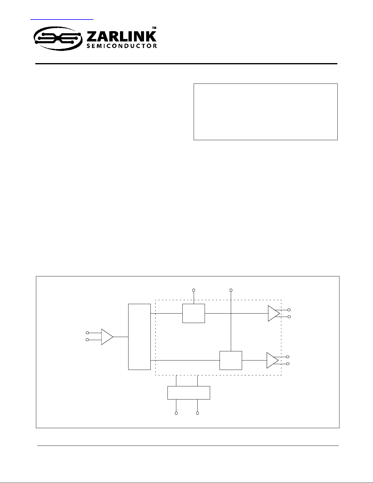
Description
The SL2150D is a wide dynamic range front end for
tuner applications.
The device offers two buffered outputs from a single
input, where both paths contain an independently
controllable AGC and disable facility.
RFINPUT
RFINPUTB
AGC1 AGC2
AGC
Control
Power
Splitter
AGC
Control
Power Down
DIS1 DIS2
Figure 1 - SL2150D Block Diagram
1
Zarlink Semiconductor Inc.
Zarlink, ZL and the Zarlink Semiconductor logo are trademarks of Zarlink Semiconductor Inc.
Copyright 2002-2005, Zarlink Semiconductor Inc. All Rights Reserved.
RFOUT1
RFOUT1B
RFOUT2
RFOUT2B
SL2150D Data Sheet
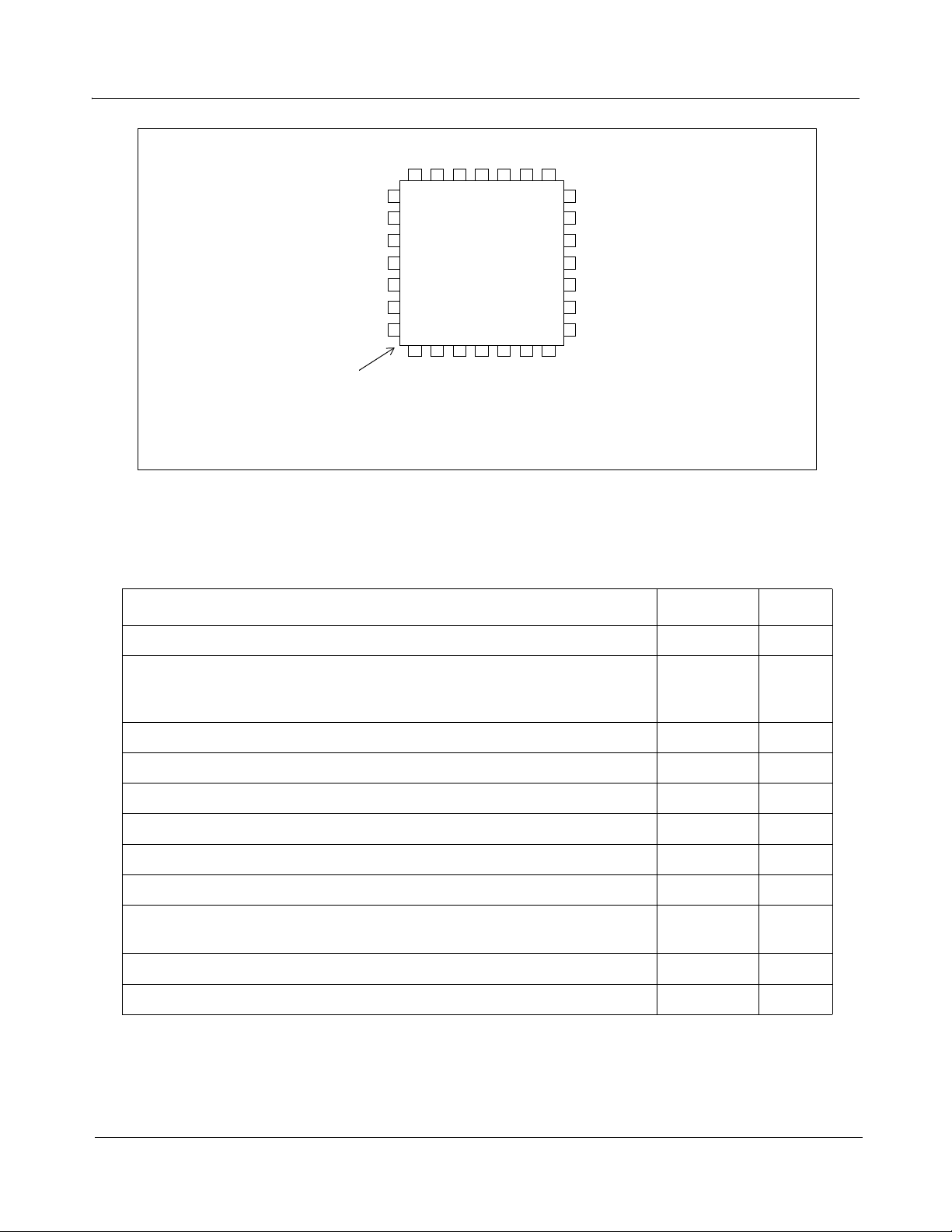
Vcc
Vcc
NC#
NC#
NC#
Vcc
Vcc
RFOUT1
RFOUT1B
VEE
(PACKAGE
PADDLE)
Vee
Vee
SL2150D
Vcc
Vcc
Vcc
# Pins marked NC should be connected to Vee
1
Vcc
Vcc
RF INPUT
RF INPUT
Vee
DIS1
DIS2
Vee
Vee
RFOUT2
RFOUT2B
NC#
AGC2
AGC1
LH28
Figure 2 - Pin Allocation
1.0 Quick Reference Data
NB all data applies with differential termination and single ended source both of 75 Ω.
Characteristics Units
RF input operating range 50-860 MHz
Gain with external load as in Figure 11
maximum
minimum
11
-25
Input NF, both paths enabled at maximum gain 6.4 dB
CTB, both paths enabled, all gain settings * -66 dBc
CSO, both paths enabled, all gain settings * -64 dBc
CXM, both paths enabled, all gain settings * -60 dBc
Input impedance 75 Ω
Input VSWR 8 dB
Output impedance differential, all loops
440 Ω
(requires external load for example as in Figure 11)
Input to output isolation (both outputs) 30 dB
Output to output isolation 25 dB
Table 1 - Reference Data
*132 channel matrix at +15 dBmV per channel, 75 Ω source impedance
dB
dB
2
Zarlink Semiconductor Inc.

SL2150D Data Sheet
2.0 Functional Description
The SL2150D is a broadband wide dynamic range dual output tuner front en d LNA with AGC. It also has application
is any system where a wide dynamic range broadband power splitter is required.
The pin assignment is contained in Figure 2 and the block diagram in Figure 1.The port internal peripheral circuits
are contained in Figure 14.
In normal application the RF input is interfaced to the device input. The input preamplifier is designed for low noise
figure, within the operating region of 50 to 860 MHz and for high intermodulation distortion intercept so offering
good signal to noise plus composite distortion spurious performance when loaded with a multi carrier system. The
preamplifier also provides an impedance match to a 75 Ω source; the typical impedance is shown in Figure 4.
The input NF is shown in Figure 6.
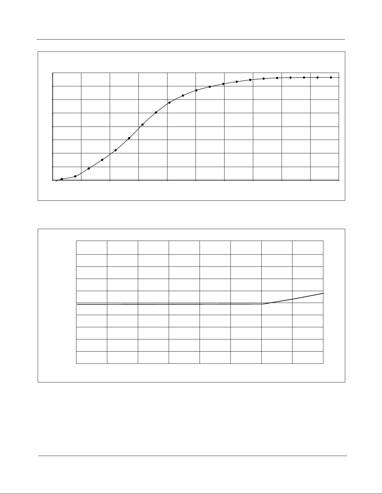
The output of the preamplifier is then power split to two independently controlled AGC stages. Each AGC stage
provides for a minimum of 30 dB of gain control across the input frequency range. The typical AGC characteristic
and NF versus gain setting are contained in Figure 5 and Figure 7 respectively.
Finally each of the AGC stages drive an output buffer of differential output impedance of 440 Ω, which provides a
nominal 11 dB of gain when terminated into a differential 75 Ω load, as in Figure 11. Each channel AGC and output
buffer can be independently powered down.
In application it is important to avoid saturation of the output stage, therefore it is recommended that the output
standing current be sunk to Vcc through an inductor. A resistive pull up can also be used as shown in Figure 13 "Example Application Driving 100 W Load with Resistive Pull Up", however the resistor values should not exceed
20 ohm single ended.
If an inductive current sink is used the maximum available gain from the device is circa 26 dB. This gain can be
reduced by application of an external load between the differential output ports. The gain can be approximately
calculated from the following formula:
- GAIN = 20*log ((Parallel combination of 440 ohm and external load between ports)/22 ohm)+2 dB
For example when driving a 100 ohm load as in Figure 12, the gain equals
- GAIN = 20 *log ((440 *100)/(440+100)/22)+2 dB =12 dB.
3
Zarlink Semiconductor Inc.
SL2150D Data Sheet
F TYPE
RFIN
CH1 S11 1 U FS
PRm
Cor
Avg
16
Smo
Z
0
75
5.1nH
1nF
3
RF INPUT
SL2150D
1nF
4
RF INPUTB
MABAES0029
1:1
Figure 3 - Input Network
4_: 133.23 55.758 10.44 nH
Ω
16 Nov 2001 10:10:47
Ω
850.000 000 MHz
4
Ω
1_: 169.02
-44.117
2_: 49.916
-57.436
250 MHz
3_: 31.238
-5.5576
500 MHz
50 MHz
Ω
Ω
Ω
Ω
Ω
Ω
3
2
START 50.000 000 MHz STOP 850.000 000 MHz
1
Figure 4 - Typical Single-end Input Impedance
4
Zarlink Semiconductor Inc.
SL2150D Data Sheet
Typical AGC vs Control Voltage
15
5
-5
-15
-25
Gain (dB)
-35
-45
-55
-65
0.5 0.7 0.9 1.1 1.3 1.5 1.7 1.9 2.1 2.3 2.5
Figure 5 - Typical AGC Characteristic
AGC Voltage (V)
Typical Noise Figure vs Frequency (Vagc = 3 V, Maximum Gain)
9
8.5
8
7.5
7
6.5
NF(dB)
6
5.5
5
4.5
4
50 150 250 350 450 550 650 750 850
Frequency (MHz)
Figure 6 - Input Noise Figure at 25°C
5
Zarlink Semiconductor Inc.

SL2150D Data Sheet
Typical Variation in Noise Figure vs. Gain Setting
20
18
16
14
12
Noise Figure (dB)
10
8
6
-10 -8 -6 -4 -2 0 2 4 6 8 10 12
Gain (dB)
Figure 7 - Typical Variation in NF versus Gain Setting
6
Zarlink Semiconductor Inc.

SL2150D Data Sheet
132 channel matrix, 75 ohm source, all channels at +15 dBmV. Input and output conditions as in Fig. 3 and Fig. 12.
-50
-60
CSO,CTB (dBS)
-70
CSO (dBC)
CTB (dBC)
-80
-20-15-10-50
Figure 8 - Typical Variation In CSO and CTB Versus Backoff from Maximum Gain
50 Ω
Driven
output
stage
Monitored
output
stage
C
D
C
D
Directional coupler
phase relationship
AB
C0 0
D180 0
Directional
coupler
Directional
coupler
A
B
A
B
50 Ω
Port 1
Network
Analyzer
Port 2
Figure 9 - Test Condition for Output Crosstalk
7
Zarlink Semiconductor Inc.

Driven
output
stage
SL2150D Data Sheet
50 Ω
C
Directional
D
coupler
A
B
Port 1
SL2150D
Monitored
input
stage
Directional coupler
phase relationship
AB
C0 0
D180 0
Network
Analyzer
Port 2
Figure 10 - Test Condition for Output to Input Crosstalk
Vcc
100nF 100pF
MABAES0029
1:1
To 75Ω load
1nF
Figure 11 - Example Application Driving 75 Ω Load
8
Zarlink Semiconductor Inc.
FTYPE

SL2150D Data Sheet
10 µH10µH
Vcc
1nF
SL2150D
1nF
100 Ω
Figure 12 - Example Application Driving 100 Ω Load with Inductive Pull Up
Vcc
2x
20 Ω
1nF
SL2150D
100 Ω
Note: External resistor
values must not exceed 20Ω
1nF
Figure 13 - Example Application Driving 100 Ω Load with Resistive Pull Up
9
Zarlink Semiconductor Inc.

SL2150D Data Sheet
Vcc
440
Ω
3.9 V
32 mA 32 mA
Output Ports
1.6 V
440
Ω
Output
30 k
Ω
INPUT
2.5 V
2.5 V
1 k
270
1 k
Ω
AGC
INPUT
INPUT
DECOUPLED
Ω
Ω
RF Input Port
20 k
Ω
1.5 V
AGC
INPUT
1.5 k
Ω
AGC Port
1.7 k
Ω
DIS Port
Figure 14 - Port Peripheral Circuitry
10
Zarlink Semiconductor Inc.

SL2150D Data Sheet
3.0 Electrical Characteristics
Test conditions (unless otherwise stated).
T
=-20o to 85oC, Vee=0V, Vcc=5V+-5%
amb
These characteristics are guaranteed by either production test or design.
They apply within the specified ambient temperature and supply voltage unless otherwise stated.
Electrical Characteristics
Characteristic Pin Min. Typ. Max. Units Conditions
Supply current 190
110
42
Input frequency
range
Input impedance 3, 4 75 Ω See Figure 4
Input return loss 6.8 8 dB See Figure 4
Input Noise
Figure
Variation in NF
with gain adjust
Gain
maximum
minimum
minimum
50 860 MHz
6.4 7.2 dB Tamb = 27°C,
9.5 11
-50
220
140
60
-1 dB/dB See Figure 7
12.5
-25
mA
mA
mA
dB
dB
dB
Both outputs enabled
One output enabled
Both outputs disabled
see Figure 6
All loops at maximum
gain
Power gain from 75 Ω
single ended source to
differential 75 Ω load,
with application as in
Figure 11.
Vagcip = 3.0 V
Vagcip = 0.5 V
Vagcip = Vee
AGC monotonic from
Vee to Vcc.
Refer to Functional
description section for
information on
calculating maximum
gain with other load
conditions
CSO -66
-62
CTB -65
-62
CXM -60 dBc See note (2)
Input P1dB +4.5 dBm All gain settings, with
11
Zarlink Semiconductor Inc.
dBc
dBc
dBc
dBc
See note (2)
See note (3)
See note (2)
See note (3)
load as in Figure 11

SL2150D Data Sheet
Electrical Characteristics (continued)
Characteristic Pin Min. Typ. Max. Units Conditions
Gain variation
within channel
Output
impedance
Output port DC
standing current
AGC1, 2 input
leakage current
DIS1, 2 input
Input high voltage
Input low voltage
Leakage current
Crosstalk
between outputs
0.25 dB Channel bandwidth
8 MHz within operating
frequency range, all
loops, all gain settings
11,12,
440 Ω Differential
24,25
11,12,
24,25
50 mA Standing current that
any external load has to
sustain.
8,9 -200 200 µA Vagcip = Vee to Vcc
6, 7
2.8
Vee
-200
Vcc
0.8
200
V
V
µA
Output disabled
Output enabled
DIS1, 2 = Vee to Vcc
-25 dB All gain settings,
measured differential
output to differential
output, driven ports in
phase and monitored
ports out of phase, see
Figure 9
Crosstalk
between outputs
and RF input
-30 dB All gain settings,
measured differential
output to single ended
input, driven ports in
phase, see Figure 10
Note 1: All power levels are referred to 75
Note 2: Load as in Figure 11and Figure 12, at maximum gain, 132 channel matrix, 75 ohm source with all channels at +15 dBmV,
Note 3: Load as in Figure 11 and Figure 12, all gain settings, 132 channel matrix, 75 ohm source with all channels at +15 dBmV,
assuming power match.
assuming power match.
Ω, and 0 dBm = 109 dBµV.
12
Zarlink Semiconductor Inc.

SL2150D Data Sheet
Absolute Maximum Ratings All voltages are referred to Vee at 0V
Characteristic Min. Max. Units Conditions
Supply voltage -0.3 6 V
RF input voltage 8 dBm Differential
All I/O port DC offsets -0.3 Vcc+0.3 V
Storage temperature -55 150
Junction temperature 125
Package thermal resistance, chip to
35
ambient
Power consumption at 5.25 V 1155 mW
ESD protection 1.5 kV Mil-std 883B method 3015 cat1
o
C
o
C Power applied
o
C/W Paddle to be soldered to
ground plane
13
Zarlink Semiconductor Inc.

4.0 Application Diagram
SL2150D Data Sheet
Figure 15 - SL2150D Evaluation PCB Schematic
14
Zarlink Semiconductor Inc.
Note: Baluns are only required to interface to 75/50 ohm test equipment.


For more information about all Zarlink products
visit our Web Site at
www.zarlink.com
Information relating to products and services furnished herein by Zarlink Semiconductor Inc. or its subsidiaries (collectively “Zarlink”) is believed to be reliable.
However, Zarlink assumes no liability for errors that may appear in this publication, or for liability otherwise arising from the application or use of any such
information, product or service or for any infringement of patents or other intellectual property rights owned by third parties which may result from such application or
use. Neither the supply of such information or purchase of product or service conveys any license, either express or implied, under patents or other intellectual
property rights owned by Zarlink or licensed from third parties by Zarlink, whatsoever. Purchasers of products are also hereby notified that the use of product in
certain ways or in combination with Zarlink, or non-Zarlink furnished goods or services may infringe patents or other intellectual property rights owned by Zarlink.
This publication is issued to provide information only and (unless agreed by Zarlink in writing) may not be used, applied or reproduced for any purpose nor form part
of any order or contract nor to be regarded as a representation relating to the products or services concerned. The products, their specifications, services and other
information appearing in this publication are subject to change by Zarlink without notice. No warranty or guarantee express or implied is made regarding the
capability, performance or suitability of any product or service. Information concerning possible methods of use is provided as a guide only and does not constitute
any guarantee that such methods of use will be satisfactory in a specific piece of equipment. It is the user’s responsibility to fully determine the performance and
suitability of any equipment using such information and to ensure that any publication or data used is up to date and has not been superseded. Manufacturing does
not necessarily include testing of all functions or parameters. These products are not suitable for use in any medical products whose failure to perform may result in
significant injury or death to the user. All products and materials are sold and services provided subject to Zarlink’s conditions of sale which are available on request.
Purchase of Zarlink’s I
conforms to the I
Zarlink, ZL and the Zarlink Semiconductor logo are trademarks of Zarlink Semiconductor Inc.
Copyright Zarlink Semiconductor Inc. All Rights Reserved.
2
C components conveys a licence under the Philips I2C Patent rights to use these components in and I2C System, provided that the system
2
C Standard Specification as defined by Philips.
TECHNICAL DOCUMENTATION - NOT FOR RESALE
 Loading...