

YORKVILLE AudioPro AP3000 Service Manual
3
HIGH EFFICIENCY STEREO POWER AMPLIFIER
000
WORLD HEADQUARTERS
CANADA
Yorkville Sound
550 Granite Court
Pickering, Ontario
L1W-3Y8 CANADA
Voice: (905) 837-8481
Fax: (905) 837-8746
Quality and Innovation Since 1963
U.S.A.
Yorkville Sound Inc.
4625 Witmer Industrial Estate
Niagara Falls, New York
14305 USA
Voice: (716) 297-2920
Fax: (716) 297-3689
SERVICE MANUAL
Printed in Canada
VERSION 1.50 October 1998
IMPORTANT SAFETY INSTRUCTIONS
AUDIOPRO AP-3000 SERVICE MANUAL
M1012 “THE INPUT BOARD”
The input board processes the audio signal from the input jacks to the voltage amplifier board, (M1011).
INSTRUCTIONS PERTAINING TO A
RISK OF FIRE, ELECTRIC SHOCK, OR
INJURY TO PERSONS.
CAUTION:
TO REDUCE THE RISK OF ELECTRIC SHOCK,
DO NOT REMOVE COVER (OR BACK).
NO USER SERVICEABLE PARTS INSIDE.
REFER SERVICING TO QUALIFIED
SERVICE PERSONNEL.
Read Instructions:
The
Owner's Manual
before operation of your unit.
instructions for future reference.
Packaging:
Keep the box and packaging materials, in case the unit
needs to be returned for service.
Warning:
When using electric products, basic precautions should
always be followed, including the following:
Power Sources:
Your unit should be connected to a power source only of the
voltage specified in the owners manual or as marked on the unit.
This unit has a polarized plug. Do not use with an extension cord or
receptacle unless all three blades can be fully inserted to prevent
blade exposure. Precautions should be taken so that the grounding
scheme on the unit is not defeated.
Power Cord:
The AC supply cord should be routed so that it is unlikely that it will
be damaged. If the AC supply cord is damaged
OPERATE THE UNIT
Service:
The unit should be serviced only by qualified service personnel.
should be read and understood
Please, save these
DO NOT
.
INSTRUCTIONS RELATIVES AU
RISQUE DE FEU, CHOC ÉLECTRIQUE,
OU BLESSURES AUX PERSONNES.
AVIS:
AFIN DE RÉDUIRE LES RISQUE DE CHOC
ÉLECTRIQUE, N'ENLEVEZ PAS LE COUVERT (OU
LE PANNEAU ARRIÈRE). NE CONTIENT AUCUNE
PIÈCE RÉPARABLE PAR L'UTILISATEUR.
CONSULTEZ UN TECHNICIEN
QUALIFIÉ POUR L'ENTRETIENT.
Veuillez lire le manuel:
Il contient des informations qui devraient êtres comprises
avant l'opération de votre appareil. Conservez S.V.P. ces
instructions pour consultations ultérieures
Emballage:
Conservez la boite au cas ou l'appareil devait être
retourner pour réparation.
Warning:
Attention: Lors de l'utilisation de produits électrique,
assurez-vous d'adhérer à des précautions de bases
incluant celle qui suivent:
Alimentation:
L'appareil ne doit être branché qu'à une source d'alimentation
correspondant au voltage spécifié dans le manuel ou tel qu'indiqué
sur l'appareil. Cet appareil est équipé d'une prise d'alimentation
polarisée. Ne pas utiliser cet appareil avec un cordon de
raccordement à moins qu'il soit possible d'insérer complètement
les trois lames. Des précautions doivent êtres prises afin d'eviter
que le système de mise à la terre de l'appareil ne soit désengagé.
Cordon d'alimentation:
Évitez d'endommager le cordon d'alimentation.
L'APPAREIL
si le cordon d'alimentation est endommagé.
Service:
Consultez un technicien qualifié pour l'entretien de votre appareil.
N'UTILISEZ PAS
Each channel consists of a balanced gain stage, defeatable bass boost filter, and a preemphasis filter network.
The balanced input, (XLR Jack) and unbalanced input (phone jack) are wired in parallel to the input of a balanced
operational amplifier, (U1). The gain of this stage is 1.6 (4dB) balanced and 1.6 (4dB) unbalanced. Resistors R1, R5
along with capacitors C1 and C2 form a radio interference elimination filter.
Switch S1 selects a flat or bass boosted frequency response. The bass boost filter provides a 20Hz high pass, high Q
filter response with a +4dB peak at 55Hz. The filter consists of a tee network on the input of U1A along with R9, R10,
R11, C5 and C6. The gain is 1 (0dB) in the passband, (above 100Hz).
Operational amplifier U3B is a high pass shelving filter with a +2dB shelf above 20KHz. This filter provides the preemphasis required to obtain a flat frequency response (to 20KHz) on the power amplifier output at full power.
M1011 "VOLTAGE AMPLIFIERS AND SYSTEM CONTROL"
This board contains:
• Voltage amplifiers to drive the current amplifiers on the M1002 boards.
• The front panel volume control circuitry.
• The EMS control system with its associated circuits: Pre clipping and line current sensing heater circuits.
• Clip and activity LED's. Driver circuitry for the amplifier disable relay (used during amplifier turn on, turn off,
thermal shutdown and current limiting).
Circuit Explanation:
Refer to the schematic of M1011 as the sections of the circuit are explained.
The audio signal enters the board from M1012 through connector MS4. The two channels are marked "L" and "R" for
left and right. The signals are to be considered as differential sources and therefore are marked as L+, L-,R+ and R-.
Since the left channel has the same topology as the right channel we will only look at the left channel.
The signal ("L+") at the terminal block (MS4) passes through the front panel level control (P1) and the desired level
enters the inverting input of U1.
Op amp U1 is an inverting amplifier with a set gain of 2.40 (7.6dB). Built around U1 is a dual purpose circuit controlled
by a voltage divider consisting of R15, R16, R17, R18, R19, R20 and R21. The voltage divider sets two reference
levels, (HDRM & CLP). Reference voltage levels vary with the voltage levels on the +/-100VDC supply rails. As the
amplifier?s output is loaded, the supply rails voltage decreases and so do the reference levels.
Transistors Q1, Q3 the surrounding resistors provide a pre-clipping function that tracks the supply rails through the
HDRM voltage reference and clips the audio signal at approximately 11.2V pk. The clip LED indicator circuit is
connected through D1 and D2 to the output of U1, The bases of Q2 and Q4 are connected to the “CLP” reference
voltage, and when the peak output voltage of U1 (+/-Vp) is enough to forward bias the transister junctions, Q2 or Q4
will trigger the clip led circuit (Q5), and eliminate the clip LED.
safe_v3.doc Version 3.5 Mar 98
1

SHUTDOWN CIRCUIT:
The audio signal on the output of U1 enters U3 through R43 and RV1. Under normal operating conditions the gain of
U3 is 1(0dB). The signal then passes through U2 to the voltage amplifier.
VOLTAGE AMPLIFIER:
The voltage amplifier amplifies the audio signal?s voltage from 6.5 volts peak (at the output of U2) to approximently
70v peak which is required to drive the current amplifier board M1002. M1002 provides the current required for the
70v peak signal to drive 1200 watts into 2 ohms out of the binding posts.
Before the circuit is described in detail here is a quick rundown on the signal?s path through the voltage amplifier
stage. Refer to the schematic of M1011. Let's consider that a positive going AC signal is present @ test point 3. The
positive going signal will turn on the positive side of the voltage amplifier. The signal at test point 3 turns on Q12
(through R40, D14 and D13). The collector of Q12 pulls down on the base of Q14, turns this transistor on further and
allows a greater current to flow out of Q14?s collector. This increase in current passes through Q15 and it?s collector to
emitter voltage drop decreases. The collector of Q15 now being more positive in voltage turns the base of Q18 on
causing an increase in Q18?scoll ec tor curr ent resu lt ing in tes t poin t 5 going positive.
As the positive side of the amplifier was turning on the negative side would have been turning off. This is how test
point 5 was able to move positive following the input signal. The reverse would hold true if a negative going signal was
present on the input of the voltage amplifier.
CIRCUIT DESCRIPTION:
The voltage amplifier is a mirrored image with circuitry connected to the positive power supply rail being identical (but
opposite polarity) to the circuitry connected to the negative power supply rail.
For this reason we will look in detail at the positive side of the amplifier.
The audio signal enters the voltage amplifier at test point 3. The signal passes through R40, D14 and D13 to the base
of Q12. Diodes D13 and D14 set up the DC bias on Q12 to approximately 0.6 mA.
The first voltage gain stage consists of Q12 along with the resistor chain on its collector and the emitter resistor (R44).
Transistor Q12 drives the base of Q14 through the resistor chain. A DC current of approximately 6 mA should flow
through the collector of Q14. The voltage drop across Q14 remains constant and is derived from the voltage drop
across the voltage reference Q20, resistor R58, and the base/emitter junction of Q15. This total voltage should equal
approximately 3 VDC. Transistor Q14 is the second gain stage and its output current flows through Q15. Transistor
Q15 is a common base stage with the collector driving the base of output buffer Q18.
The last circuit on board M1011 is the shutdown relay and its associated drive circuitry. The relay circuit has two
possible operating states.
1. Amplifier on under normal operating conditions.
2. Amplifier power switch has just been turned OFF/ON or the amplfier is in current limit protecting the amplifier?s
output or the amplifier has overheated.
CIRCUIT DESCRIPTION
Here is how the circuit accomplishes these functions. The relay?s normally closed contacts short the output of the
voltage amplifiers to ground when the power switch is off. When the power switch is turned on, the relay remains off
(normally closed) for about 6 seconds. C52 charges to 35V and results in Q37 turning off allowing Q36 to turn on. As
Q36 turns on, it connects the negative terminal of the relay?s coil (Pin 16) to ground energizing the relay and opening
the normally closed contacts.
If prolonged current limiting occurs on the amplifier?s output transistors then D50 or D51 (depending on which channel
is current limiting) will be forward biased turning on Q38 (from its off state). Now +100VDC appears on the collector of
Q38 and through R130 and R128 turn on Q37 therefore turning off Q36 by shorting its base emitter junction. Q36
turning off will turn the relay off and the normally closed contacts (off state) will short the outputs of the voltage
amplifiers to ground so as not to continuously stress the amplifier?s output transistors. A cycle now occurs. With the
voltage amplifiers now disabled there is no signal driving the output transistors (Q14 to Q28) on board M1002.
The current limit circuit on M1002 turns off and D50 and/or D51 are not forward biased and Q38 turns off. Through
Q37 and Q36 the relay is turned back on and the voltage amplifiers are now active again, driving the output
transistors. If current limiting still occurs, then the same cycle will occur. If the cause of current limiting (low impedance
or short on the speaker output terminals) has been removed, then the amplifier will continue to operate normally.
The third operation that the relay provides is "overheat shutdown". If for some reason the fan cannot keep the
heatsinks in a safe operating temperature area then the fan control circuit (on board M1013) will deliver through the
"kill" signal line a positive current to turn Q37 on and turn Q36 off to turn off the relay and disable the voltage
amplifiers. When the temperature of the amplifier has been cooled down by the fan, then the kill signal will disappear
and the relay circuit will turn on the relay to resume normal operation. Anytime the relay is in the "protect" mode (due
to the abnormal states) then contact pin 8 of the relay will illuminate LD5 (the protect LED on the front panel).
M1002 “CURRENT AMPLIFIER BOARD”
The current amplifier board (M1002) receives a high voltage audio signal from voltage amplifier board (M1011) and
provides the current drive necessary to drive speaker cabinets.
Diode D17 is a clamping diode that prevents the maximum peak of the audio signal from coming within 4V of the 100
VDC rail. This is to prevent the output current amplifier (board M1002) from going into saturation during clipping and
therefore having storage delay problems.
Transistor Q18 buffers the high impedance present on the collector of Q15. The output of the buffer provides a low
output impedance at test point 5 and is current limited to 38mA through the clamping action of D19, D20 and D23.
The signal at TP-5 drives the current amp board M1002.
DC offset on the amplifier?s output is corrected by operational amplifier U2. The DC offset forms a current through
R54, R14 and is blocked by C5 giving a DC offset correction gain of -1.
The activity L.E.D. function is a simple charge pump circuit with a transistor that redirects a constant current path
through the activity L.E.D.
2
The current amplifier is a two tier complimentary output driver design controlled by a complimentary mos-fet stage.
CIRCUIT DESCRIPTION - REFER TO THE SIMPLIFIED SCHEMATIC #1 ON THE FOLLOWING PAGE
3
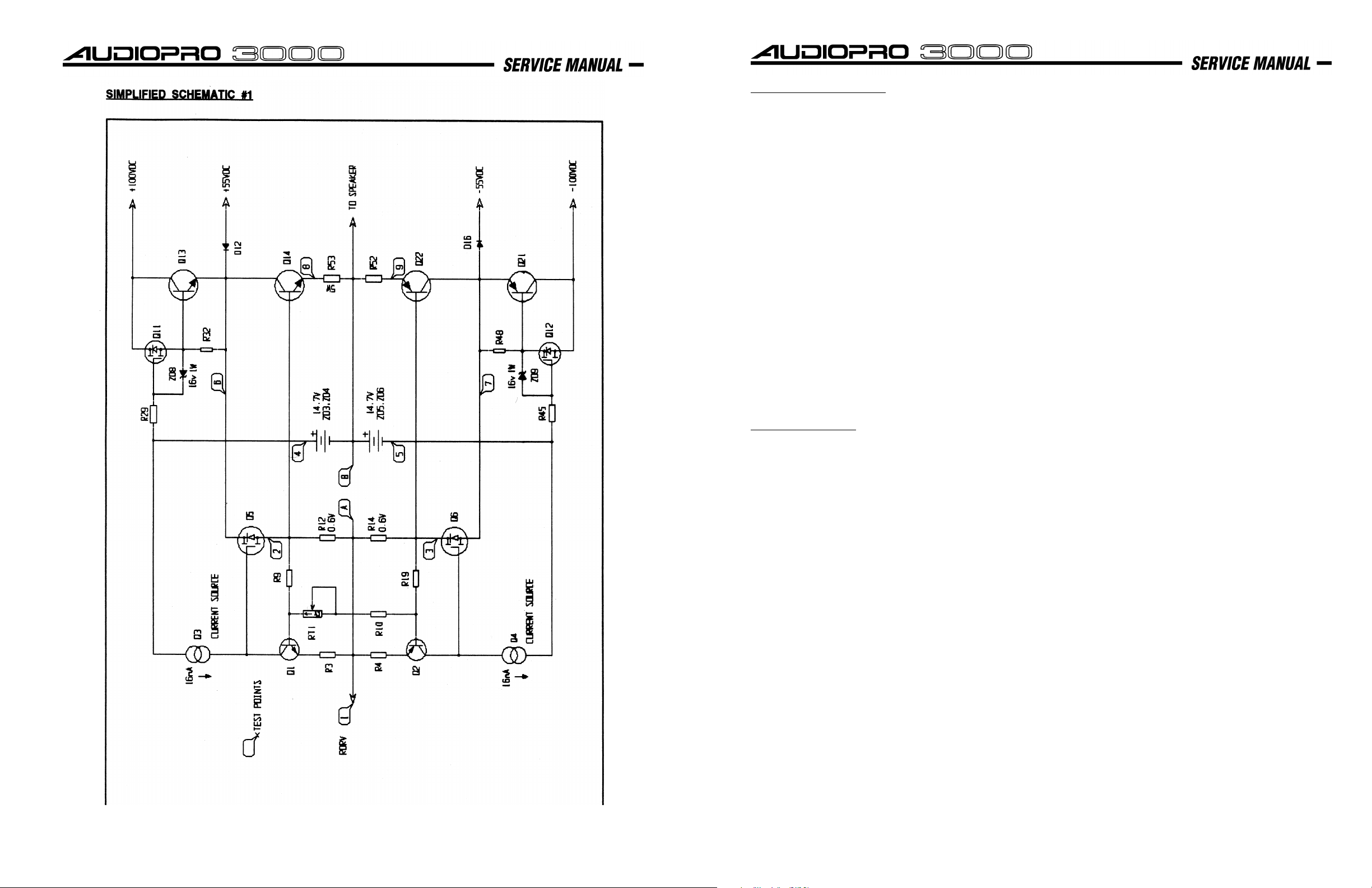
QUIESCENT CONDITION:
This design is class A/B and therefore the output driver transistors must be forward biased to provide low crossover
distortion. In most class A/B designs, a diode chain or VBE multiplier is used to control the bias voltage and provide a
means of adjusting the bias. This design is different as there isn't a diode chain or VBE multiplier. For simplicity lets
consider only the positive side of the current amplifier, that is all parts between the positive power supply rails and the
audio signal output/input terminals. The negative side is the same as the positive, except for polarity changes.
To bias Q14, greater than 0.5V is needed from base to emitter, (or for simplicity from base to amplifier output). Points
A and B are at the same potential, so consider them to be connected. If this is true then 0.5V from test point 2 to the
amplifier output must appear across R12. There must be some way of developing this voltage across R12, and there
is using the mos-fet (Q5) driver along with local feedback.
Simplified schematic Fig. #1 shows the biasing circuit. The current needed to develop 0.5V across R12 comes from
the source of Q5. When the amplifier is first turned on the current source (Q3) turns on Q5 and current flows through
R12 developing a voltage. When this voltage approaches 0.5V Q1 turns on and robs current from the gate of Q5.
This causes Q5 to turn off until the reduced current flowing through Q5 maintains 0.5V across R12. Q1 will turn off
slightly causing Q5 to increase its source current. The circuit reaches a point of equilibrium with approximately 0.5V
across R12.
Because all output devices are not identical and base emitter voltages vary, some adjustment must be available to
slightly adjust the 0.5V across R12. This is accomplished with RT1. RT1 causes Q1 to turn on slightly more or less
resulting in Q5 turning on slightly more or less and therefore R12? s voltage will be slightly more or less than 0.5v. The
proper quiescent current adjustment is 4mV ( to be measured between test points 8 and 9).
THE SECOND TIER:
Refer to the simplified schematic Fig. #1 while reading the following text. One way of making an amplifier more
efficient is to vary the Power Supply Voltage on the collectors of the output transistors (Q14 & Q22). The lower the
voltage from collector to emitter, the lower the device dissipation. During quiescent conditions, there is 55VDC on the
collectors of output transistors Q14 and Q22. The peak AC voltage that can appear on the amplifier's output is
approximately 95V peak. How can an output transistor deliver a 95V peak when its collector is only at 55VDC? It can
if its collector is pulled up to 100VDC as the output signal's peak rises above 55VDC. (refer to Fig. #2). The second
tier voltage must remain above the amplifier's output voltage by amount Vm. Therefore the circuitry controlling the
second tier voltage must increase the tier voltage before the amplifier's output voltage reaches 55VDC. This leading
voltage is necessary to compensate for time lag of the second tier circuit during fast rising amplifier output signals.
4
5
The voltage between the am plifier? s
output and te st p oint 4 i s
approximately 14 .7V DC de ri ved
from the voltage drop across ZD3
@ ZD4. We call this voltage the
“floating battery” because it floats
on top of the ou tp ut au dio signal
with point 4 always being 14.7VDC
greater than the pe ak of th e out pu t
signal. Point 4 drives the gate of
mos-fet Q11. Q11 cont rols th e
transistors of the upper tier. As Q11
turns on it's source foward biases
the base of Q13 and Q13 pulls the
collector of Q14 towards the 100
volt rail. The gate to source voltage
needed to tu rn on Q 11 i s
approximately 3.5 volts. When the
peak output si gna l i s ab ou t 4 4 vp
(55v-(14.7v-3.5v)) then Q11 will
start to turn on the second ti er. Th e second tie r voltage wi ll remai n about 11 volts (Vm) above the pea k of the outp ut signal
to the point of clipping where this voltage is reduced to about 4 volts. Zener ZD8 protects the gate source junction of Q11
and also provide s a curren t pa th th ro ugh R29 fo r t he “flo at ing batt er y”.
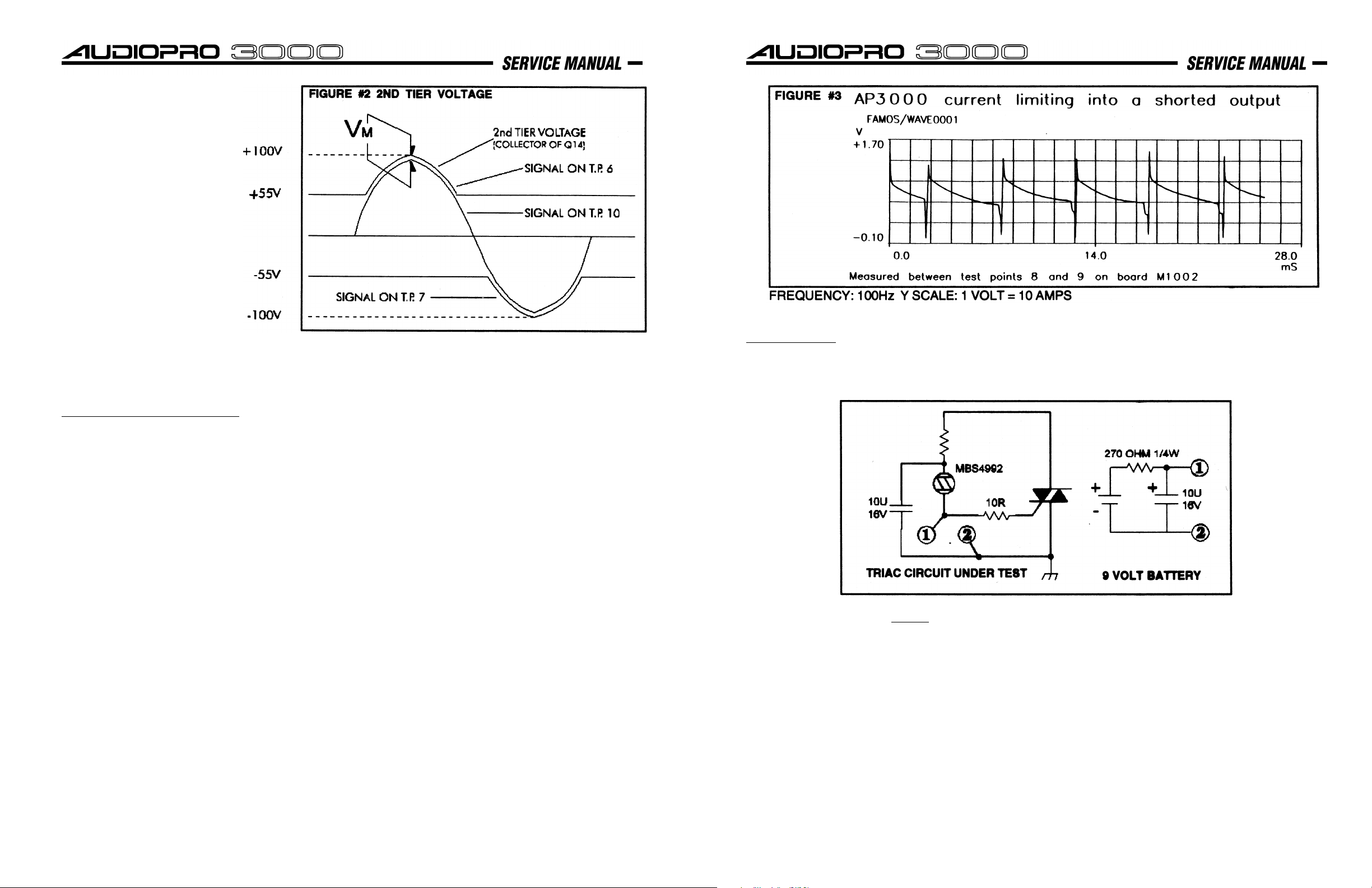
Current Limit Protection Circuitry
DC Protection
If a DC voltage greater than 8 volts appears on the output of the amplifier for more than 200 milliseconds then triac
Q30 will turn on holding the output at ground potential. MBS4992 is a device that turns on at either + or - 8 volts DC.
To have an amplifier drive 3000 watts into practically any combination of speaker cabinets and know what is a safe
load and what is not is a very difficult task. An extensive amount of time was spent on the current limit circuitry so that
it may simulate the safe operating area of the output transistors (SOAR curve). No matter how reactive the load may
be the phase shift that it presents, along with it's resistive component is used to set the output current limit of the
output transistor stage.
Refer to the schematic of board M1002 while reading the following text. The current limit circuitry is a mirrored image
with circuitry connected to the positive power supply rail being identical (but opposite polarity) to the circuitry
connected to the negative power supply rail. For this reason we will look at the positive side of the circuitry.
Transistor Q9 measures the peak current flowing through resistor R53. The voltage across R53 (as a result of the
current flowing through it) is scaled down by R55, R35, R36, R37, D7 and D11- these parts make up the safe
operating area along with the time constants of C26, R34, C12 and R26. Fig. #3 shows a waveform of the current that
passes through R52 and R53 when the output of the amplifier is shorted to ground. This can only be seen by using an
oscilloscope to measure differentially across R52 and R53. The conditions of the measurement are contained on the
diagram. During current limit when Q9 turns on it reduces the voltage across R42. R42 is in series with a 16 volt zener
(ZD7) and is also in parallel with the junction of Q8. Q8 is normally saturated by the current that flows through R20,
ZD7, R42, and R22. When Q9 reduces the voltage across ZD9 and R42 to below 16.6 volts then Q8 turns off allowing
a charge to build up on C8 through resistors R24 and R25. If current limiting occurs for a long enough duration to
allow C8 to charge to 1.2 volts then Q7 will turn on tripping the relay circuit on board M1011. As soon as the relay is
turned off the audio signal will be turned off at the voltage amplifiers and will remain off for about 5 seconds before the
relay turns on and allows the audio signal to pass through the amplifier. If a current limit condition is still present then
the whole cycle will occur again and repeat until the load condi tions on the amplifier's output are safe for the amplifier.
When a safe load reappears the amplifier will automatically reset and drive that load (the speaker cabinet).
Subwoofers present large inductive loads to the amplifier and are driven at low frequencies where the large current
peaks must be tolerated for short periods of time. To accommodate this type of loading C26 and R34 are used to
retard the firing of Q9 at low frequencies.
NOTE:
M1002 board test the DC protection triac with the following circuit.
Conditions of test:
A. Pass a 100Hz 25v peak signal through the M1002 board under test with no load connected to the amplifier output.
B. Connect points 1 and 2 as shown in the diagram. The amplifier should go into protect mode as the triac ( if
working) shorted the output of the amplifier to ground, and the amplifier goes into current limit.
C. Disconnect the triac test circuit and allow the amplifier to complete it?s protect cycle.
D. Reverse connections 1 to 2 and 2 to 1 and test again. The same results as in B) should be observed if the triac is
working.
Only test the triac for one protect cycle as prolonged testing will heat the triac to a high temperature.
Everytime you replace blown output transistors on a
6
7
 Loading...