

YOBON YB1680 Technical data

YB1680
1.5MHz, 600mA Synchronous Step-Down Converter
Description
The YB1680 is a 1.5MHz constant
frequency, slope compensated current
mode PWM step-down converter. The
device integrates a main switch and a
synchronous rectifier for high efficiency
without an external Schottky diode. It is
ideal for powering portable equipment that
runs from a single cell lithium-Ion (Li+)
battery. The YB1680 can supply 600mA of
load current from a 2.5V to 5.5V input
voltage. The output voltage can be
regulated as low as 0.6V. The YB1680 can
also run at 100% duty cycle for low dropout
operation, extending battery life in portable
system. Idle mode operation at light loads
provides very low output ripple voltage for
noise sensitive applications.
The YB1680 is offered in a low profile 5-pin,
SOT package, and is available in an
adjustable version.
Features
High Efficiency : Up to 94%
1.5MHz Constant Switching Frequency
600mA Output Current at V
Integrated Main Switch and Synchronous
=3V
IN
Rectifier. No Schottky Diode Required
2.5V to 5.5V Input Voltage Range
Output Voltage as Low as 0.6V
100% Duty Cycle in Dropout
Low Quiescent Current : 300μA
Slope Compensated Current Mode
Control for Excellent Line and Load
Transient Response
Short Circuit Protection
Thermal Fault Protection
<1μA Shutdown Current
Space Saving 5-Pin SOT23 Package
Pb-free Package
Applications
Cellular and Smart Phones
Microprocessors and DSP Core Supplies
Wireless and DSL Modems
PDAs
MP3 Player
Digital Still and Video Cameras
Portable Instruments
T ypical Applicatio n Circuit
Figure 1: Typical Application Circuit
YB1680 Rev.1.0 www.yobon.com.tw 1
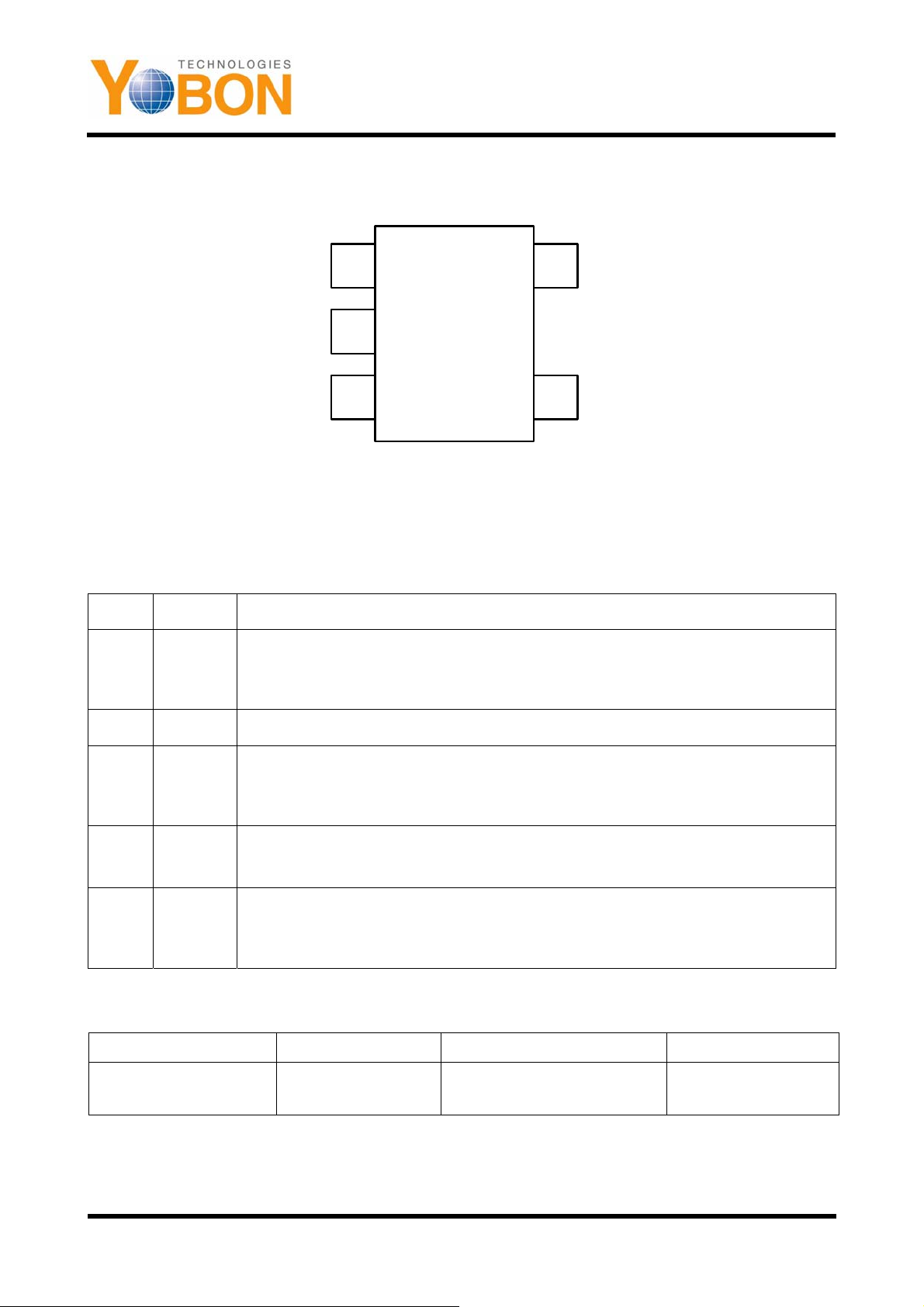
Pin Configuration
YB1680
1.5MHz, 600mA Synchronous Step-Down Converter
EN
GND
SW
1
2
3
SOT23-5
Figure 2: Pin Configuration
5
4
Pin Description
Table 1
Pin Name Description
Regulator Enable control input. Drive EN above 1.5V to turn on the
1 EN
part. Drive EN below 0.3V to turn it off. In shutdown, all functions are
disabled drawing <1μA supply current. Do not leave EN floating.
FB
VIN
2 GND Ground.
Power Switch Output. It is the Switch note connection to Inductor. This
3 SW
4 VIN
5 FB
pin connects to the drains of the internal P-CH and N-CH MOSFET
switches.
Supply Input Pin. Must be closely decoupled to GND, Pin 2, with a
2.2μF or greater ceramic capacitor.
VFB (Adjustable Version) : Feedback Input Pin. Connect FB to the
center point of the external resistor divider. The feedback threshold
voltage is 0.6V.
Ordering Information
Order Number Package Type Supplied As Package Marking
YB1680ST25XADJP SOT23-5 3000 units Tape & Reel A1XY (Note 1)
Note 1: XY = Manufacturing Date Code
YB1680 Rev.1.0 www.yobon.com.tw 2

1.5MHz, 600mA Synchronous Step-Down Converter
Absolute Maximum Ratings
YB1680
Input Supply Voltage................... -0.3V to 6V
EN, VFB Voltage ................ -0.3V to VIN+0.3V
SW, V
Voltage.............. -0.3V to VIN+0.3V
OUT
Peak SW Sink and Source Current........1.5A
Electrical Characteristics
Table 2 (V
Input Voltage Range
Input DC Supply Current
Active Mode
Shutdown Mode
Regulated Feedback Voltage
VFB Input Bias Current
= V
IN
= 3.6V, TA=25°C, Test Circuit Figure 1, unless otherwise noted.)
RUN
Description Symbol Test Conditions MIN TYP MAX Units
V
IN
I
V
Q
= 0.5V
FB
V
= 0V, VIN = 4.2V
FB
TA = +25℃
V
FB
I
FB
TA = 0℃ ≦ TA ≦ 85℃
T
= -40℃ ≦ TA ≦ 85℃
A
V
= 0.65V
FB
Operating Temperature Range.. -40°C to 85°C
Junction Temperature ....................... 125°C
Storage Temperature Range ... -65°C to 150°C
Lead Temperature (Soldering, 10s) .. 300°C
2.5 5.5 V
270
0.08
0.5880 0.6000 0.6120
0.5865 0.6000 0.6135
0.5850 0.6000 0.6150
400
μA
1.0
V
±30 nA
Reference Voltage Line
Regulation
Output Voltage Line Regulation
Output Voltage Load Regulation
Maximum Output Current
Oscillator Frequency
R
R
of P-CH MOSFET
DS(ON)
of N-CH MOSFET
DS(ON)
Peak Inductor Current
SW Leakage
Output Over Voltage Lockout
EN Threshold
EN Leakage Current
V
= 2.5V to 5.5V,
F
OSC
FB
V
OUT
V
= 2.5V to 5.5V, I
IN
I
OUT
VIN = 3.0V
V
FB
ISW = 300mA
ISW = -300mA
= 3V, V
V
IN
V
OUT
= VFB (R2=0)
OUT
from 0 to 600mA
= 0.6V or V
FB
= 100%
OUT
= 0.5V or
= 90%
= 10mA
0.11 0.63 %/V
0.11 0.63 %/V
0.0015 %/mA
600 mA
1.2 1.5 1.8 MHz
0.30 0.50 Ω
0.20 0.45 Ω
1.20 A
Duty Cycle < 35%
= 0V, V
V
RUN
V
= 5V
IN
ΔV
= V
OVL
-40℃ ≦ T
V
EN
I
EN
= 0V or 5V,
SW
- VFB
OVL
≦ 85℃
A
±0.01 ±1 μA
60 mV
0.3 0.45 1.30 V
±0.1 ±1 μA
YB1680 Rev.1.0 www.yobon.com.tw 3
 Loading...