

GMOS Technology
Crop. www.gmos
-
semi.com
■
General
Descr
iption
circuits
that provide
all the active
functions
for a
include
a
guaranteed
+4%
tolerance
on
output
voltage
under
specified
input
on
the oscillator
frequency.
The output
version
■
Features
-
-
3.3V,
5V, 12V and adjustable
output
versions
-
- - - - - - - -
Available
in
TO220
-5L
and TO263
-5L
packages
■
Applications
-
- - -
Simple
High
-
efficiency
step-down(buck)
regulator
- Battery
Charger
■
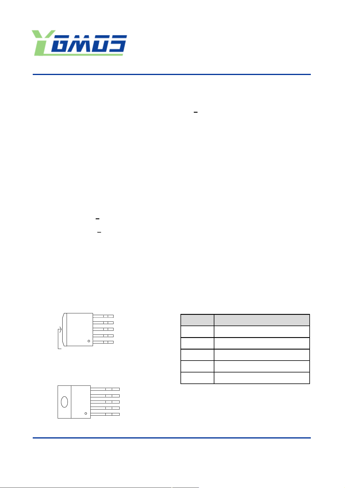
Pin
Assignments
( Top View
)
(
Top View
)
TO263
-5L 1 V
IN
5 SD
Metal Tab GND
1 V
IN
5 SD
■
Pin
Descriptions
Name
Description
V
IN
Output
Switching
output
输出
Gnd Ground
SD ON/OFF
Shutdown
使能
GT1500
150Khz, 3A PWM Buck Switching Regulator
The
GT1500 series are monolithic integrated
Adjustable version output voltage range, 1.23V to
step-down DC/DC converter, capable of driving a
3A load without additional transistor component.
Requiring a minimum number of external
component, the board space can be saved easily.
The external shutdown function can be controlled
by TTL logic level and then come into standby
mode. The internal compensation makes feedback
control have good line and load regulation without
external design. Regarding protected function,
thermal shutdown is to prevent over temperature
operating from damage, and current limit is against
over current operating of the output switch. The
GT1500 series operates at a switching frequency of
150Khz thus allowing smaller sized filter
components than what would be needed with lower
frequency switching regulators. Other features
voltage and output
load conditions, and +15%
included fixed 3.3V,
5V, 12V, and an adjustable type. The packages are
available in a standard 5-lead TO-220(T) package
and a 5-lead TO-263(S).
28V +4% max over line and load condiction
Voltage mode non-synchronous PWM control
Thermal-shutdown and current-limit protection
ON/OFF shutdown control input
Input voltage range up to 32V
Output load current: 3A
150 kHz fixed frequency internal oscillator
Low power standby mode
Built-in switching transistor on chip
Efficient preregulator for linear regulators
On-card switching regulators
Positive to negative converter
脚位排列
4 FB
3 Gnd
2 Output
TO220-5L
1/10
4 FB
3 Gnd
2 Output
Operating voltage input 输入脚
地
FB Output voltage feedback control反馈
GT1500
GMOS Technology
Corp. www.gmos
■
Ordering
Information
Package
GT1500
XX X X
Packing
Blank
:
Tube
A :
Taping
Blank
:
Adjustable
■
Block
Diagram
+ + + _
Output
SD
FB
+
150Khz, 3A PWM Buck Switching Regulator
Output version
T: TO220-5L
-33 : 3.3V
-50 : 5.0V
-12 : 12V
S: TO263-5L
Current
Source
bias
1.235V
Reference
_
Amp
2.5V
Regulator
Comp
Start
up
150kHz
OSC.
Comp
Comp
Pre-driver
Thermal
Limit
200mV
220mV
3A
Switch
V
IN
Gnd
2/10
-semi.com
GT1500
GMOS Technology
Corp. www.gmos
■
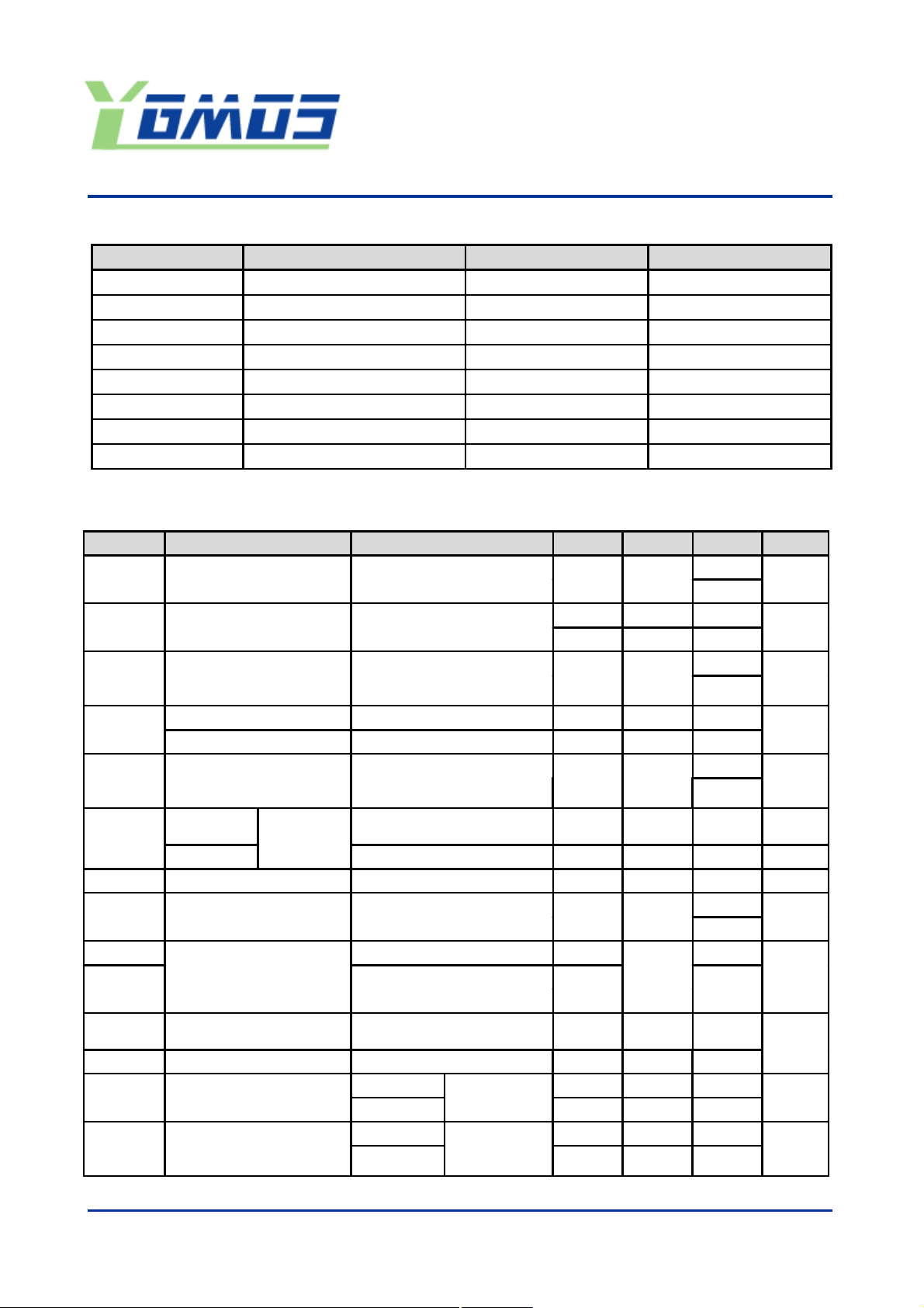
Absolute
Maximum
Ratings
Symbol
Parameter
Rating
Unit
V
CC
Supply
Voltage
+34 V V
SD
使能电压
ON/OFF
Pin input
voltage
-0.3 to +25 V V
FB
反馈电压
Feedback
Pin voltage
-0.3 to +25 V V
OUT
Output
voltage
to
Ground
-1 V P
D
Power
dissipation
Internally
limited
W T
ST
储存温度
Storage
temperature
-65 to +150
o
C T
OP
Operating
temperature
-40 to +125
o
C V
OP
Operating
voltage
+4.5
to
+25 V
■
Electrical
Characteristics
(All
Output
Voltage
Versions)
Unless
otherwise
specified,
V
=12V for 3.3V, 5V, adjustable
version
and V
=24V for the 12V version.
I
= 0.3A
Symbol
Parameter
Conditions
Min.
Typ.
Max.
Unit
60 I
B
Feedback
bias current
V
FB
=1.3V
(Adjustable
version
only)
40
100 nA 127 150 173 F
OSC
oscillator
frequency
110 173
Khz 1.4 V
SAT
saturation
voltage
I
OUT
=3A no outside
circuit
V
FB
=0V force
driver
on
1.3
1.5
V Max.
Duty
Cycle(ON)
V
FB
=0V force
driver
on
100 DC Min. Duty
cycle(OFF)
V
FB
=12V
force
driver
off 0 % 5.5 I
CL
current
limit
peak
current
no outside
cir
cuit
无外部电
V
FB
=0 force
driver
on
3.6 4.5
6.5
A Output
= 0 no
outside
circuit
V
FB
=12 force
driver
off
200 uA I
L
Output
输出
V
IN
=
32V 2 60 mA I
Q
Quiescent
Current
V
FB
=12 force
driver
off
5 10 mA
250 I
STBY
Standby
Quiescent
ON/OFF
pin=5V
Current
V
IN
=40V
150
300
uA V
IL
Low (regulator
ON)低 -
0.6 V
IH
ON/OFF
pin logic
input
High
(regulator
OFF)
2.0 1.3 - V I
H
ON/OFF
pin logic
V
LOGIC
=2.5V
(OFF)
15 25
I
L
入电流
ON/OFF
pin input
current
V
LOGIC
=0.5V
(ON)
0.02 5 uA TO220
-5L
2.5
Θ
JC
Thermal
Resistance
TO263
-5L
Junction
to
3.5
o
C/W TO220
-5L 28 Θ
JA
Thermal
Resistance
With
copper
area of approximately
3
in
2
TO263
-5L
Junction
to
23
o
C/W
150Khz, 3A PWM Buck Switching Regulator
符号
输入电压
对地输出
耗散功率
运行温度
运行电压
反馈偏流
震荡频率
参数
IN
IN
范围
单位
LOAD
仅仅适用于可调
饱和电压
无外部电路
强制驱动开
Output = 1
待机静态电流
threshold voltage
使能输入阀值电压
input current 使能输入电流
电流限度
Leakage泄漏
Current电流
静态电流
热阻
热阻
峰值电流
强制驱动开
强制驱动关
强制驱动关
高
Case 结壳
Ambient 结环
3/10
-semi.com

GT1500
GMOS Technology
Corp. www.gmos
■
Electrical
Characteristics
(Continued)
Symbol
Parameter
Conditions
Typ.
Limit
Unit
FB
V
Output
5V < V
IN
< 32V 0.2A
< I
LOAD
< 3A V
OUT
programmed
for 3V 1.23 1.193/
1.18
V V
MIN
V
MAX
GT1500
-
ADJ
Efficiency
V
IN
= 12V,
I
LOAD
=3A 73 %
OUT
V Output
voltage
5.5V
< V
IN
< 32V 0.2A
< I
LOAD
< 3A 3.3 3.168/
3.
135
V V
MIN
V
MAX
GT1500
-
3.3V
Efficiency
V
IN
= 12V,
I
LOAD
=3A 73 %
OUT
V Output
voltage
8V < V
IN
< 32V 0.2A
< I
LOAD
< 3A 5 4.8/
4.75
V V
MIN
V
MAX
GT1500
-5V
Efficiency
V
IN
= 12V,
I
LOAD
=3A 80 %
OUT
V Outp
ut voltage
15V < V
IN
< 32V 0.2A
< I
LOAD
< 3A 12 11.52/
11.4
V V
MIN
V
MAX
GT1500
-
12V
Efficiency
V
IN
= 15V,
I
LOAD
= 3A 90 %
Specifications
with boldface
type are for full operating
temperature
range,
the other type are for T =25_C.
150Khz, 3A PWM Buck Switching Regulator
反馈电压
η效率
输出电压
η效率
输出电压
η效率
输出电压
η效率
符号
Feedback
参数
条件
1.267/1.28
3.432/3.465
5.2/5.25
12.48/12.6
J
4/10
-semi.com

GT1500
GMOS Technology
Corp. www.gmos
■
Typical
Performance
Characteristics
Typical
Performance
Characteristics
V
IN
=20V, I
LOAD
=3A Normalized
at T
=25oC
JJUNCTIO
N TEMPERATURE(oC)
Switch
Current
Limit
Operating
Quiescent
Current
JUNCTION
TEMPERATURE(oC)
Efficiency
30 35 40
3A L
oad
3
SWITCH
CURRENT(A)
3
1 : -40
oC
2 : 25
oC
3 : 125
oC
Switch
Saturation
Voltage
IN
=12V,
V
OUT
=5V
Shutdown
Quiescent
Current
V
ON/OFF
=5V 1 : -40
oC
2 : 25
oC
1 3 2 Switch
ON
Switch
OFF
150Khz, 3A PWM Buck Switching Regulator
Normalized Output Voltage
5.10
5.05
5.00
4.95
4.90
-50 -25 0 25 50 75 100 125
JUNCTION TEMPERATURE(oC)
100
95
90
85
80
75
70
5V
3.3V
8 10 15 20 25
1.7
1.6
1.5
1.4
1.3
1.2
25.0
20.0
15.0
10.0
5.0
0.0
1
2
2.0
-50 -25 0
JUNCTION TEMPERATURE(oC)
25 50 75 100 125
4 5
6.0
V
5.5
5.0
4.5
4.0
-50 -25 0 25 50 75 100 125
200.0
160.0
120.0
80.0
40.0
0.0
10 20 30 40
SUPPLY VOLOTAGE (V)
3 : 125
oC
5/10
-semi.com

GT1500
GMOS Technology
Corp. www.gm
■
Typical
Performance
Characteristics
(Continued)
JUNCTION
TEMPERATURE(oC)
1.4 5 10 15 20 22 23 24 25
ON/OFF
Pin Current
(Sinking)
150.0
V
IN
=40V
-40oC
T
J
125oC
50.0
0 25 50 75
100 125
Adjustable
Version
Only
1.0
Minimum
Operating
Supply
Voltage
-50 -25 0 25 50 75 100 125
V
OUT
=1.23V
I
LOAD
=120mA
JUNCTION
TEMPERATURE
(oC)
ON/OFF
Threshold
Voltage
5.0
-50 -25 0 25 50 75
100 125
Switch
Frequency
JUNCTION
TEMPERATURE
(oC)
200.0
150Khz, 3A PWM Buck Switching Regulator
5.0
4.0
3.0
2.0
0.0
JUNCTION TEMPERATURE (oC)
4.0
3.0
2.0
1.0
0.0
120.0
90.0
60.0
30.0
0.0
Feedback Pin Bias Current
40.0
30.0
20.0
10.0
0.0
-50 -25
≤ ≤
ON/OFF PIN VOLTAGE (V)
150.0
100.0
50.0
0.0
-50 -25 0 25 50 75 100 125
os-semi.com
6/10

GT1500
GMOS Technology
Corp. www.gmos
■
Typical
Application
Circuit
1
2
4
12V
C
in
680uF
FB SD Output
Gnd
GT1500
L1
470uF
3.3V/3A
Output Load
■
Function
Description
Pin Functions
+V
IN
This is the positive
input
supply for the IC switching
regulator.
A
suitable
input
bypass
capacitor
must
be
between
(+V with
IN
V
SAT
) and approximately
0.5V,
cycle
of
approximately
V
OUT
/ V
IN
. To minimize
coupling
to
circuitry,
the PC
board
copper
area connected
to
this pin should
ON /OFF
Allows
the switching
regulator
circuit
to be
feature
is
not needed,
the ON
/OFF
pin can be
wired
to
the g
round
pin or
Thermal
Considerations
switching
regulator
in an
ambient
temperature
of 25 C
(still air). These
temperature
rise numbers
are
o
all approximate
and there
are many
factors
that can
The PC board
copper
area that
the package
is
in ,
2
inches
of 2
oz.
characteristics,
but
with
copper
areas
greater
than
in ,
2
heat dissipation
are
150Khz, 3A PWM Buck Switching Regulator
DC Input
Vin
-33
5
present at this pin to minimize voltage transients
and to supply the switching currents needed by the
regulator.
Ground
Circuit ground.
Output
Internal switch. The voltage at this pin switches
3
1N5824
The GT1500 is available in two packages, a 5-pin
TO-220 and a 5-pin surface mount TO-263.
The TO-220 package needs a heat sink under most
conditions. The size of the heatsink depends on the
input voltage, the output voltage, the load current
and the ambient temperature. The GT1500 junction
temperature rises above ambient temperature for a
3A load and different input and output voltages.
The data for these curves was taken with the
GT1500 (TO-220 package) operating as a buck
68uF
Co
D1
a duty
sensitive
be
kept a minimum.
Feedback
Senses the regulated output voltage to complete
the feedback loop.
shutdown using logic level signals thus dropping
the total input supply current to approximately
150uA. Pulling this pin below a threshold voltage of
approximately 1.3V turns the regulator on, and
pulling this pin above 1.3V (up to a maximum of
25V) shuts the regulator down. If this shutdown
it can be left open, in
either case the regulator will be in the ON condition.
7/10
-semi.com
affect these temperatures. Higher ambient
temperatures require more heat sinking.
The TO-263 surface mount package tab is
designed to be soldered to the copper on a printed
circuit board. The copper and the board are the
heat sink
for this package and the other heat producing
components, such as the catch diode and inductor.
soldered to should be at least 0.8
and ideally
should have 2 or more square
Additional copper area improves the thermal
approximately 6
only small improvements in
realized. If further thermal
improvements are needed, double sided, multilayer
PC board with large copper areas and/or airflow are
recommended.

GT
1500
GMOS Technology
Corp. www.gmos
■
Function
Description
(Continued)
The GT1500
(TO-263 package)
junction
junction
which
air, and moving
air lowers
the thermal
resistance
■
Marking
Information
(1) TO263
-5L
GT 1500
-XX
Output
Type:
Logo ID code Year: ( Top view ) "02" = 2002 "01" = 2001
YY WW ~
Xth week: 01~52
(2) TO220
-5L
GT 1500
-XX
Output
Type:
Logo ID code Year: "01" = 2001 ( Top view ) "02" = 2002
YY WW ~
Xth week: 01~52
150Khz, 3A PWM Buck Switching Regulator
temperature rise above ambient temperature with a
2A load for various input and output voltages. This
data was taken with the circuit operating as a buck
switching regulator with all components mounted on
a PC board to simulate the junction temperature
under actual operating conditions. This curve can
be used for a quick check for the approximate
temperature for various conditions, but be
aware that there are many factors that can affect
the junction temperature. When load currents
higher than 3A are used, double sided or multilayer
PC boards with large copper areas and/or airflow
might be needed, especially for high ambient
temperatures and high output voltages.
For the best thermal performance, wide copper
traces and generous amounts of printed circuit
board copper should be used in the board layout.
(Once exception to this is the output (switch) pin,
should not have large areas of copper.)
Large areas of copper provide the best transfer of
heat (lower thermal resistance) to the surrounding
even further.
Package thermal resistance and junction
temperature rise numbers are all approximate, and
there are many factors that will affect these
numbers. Some of these factors include board
size, shape, thickness, position, location, and even
board temperature. Other factors are, trace width,
total printed circuit copper area, copper thickness,
single or double-sided, multilayer board and the
amount of solder on the board. The effectiveness
of the PC board to dissipate heat also depends on
the size, quantity and spacing of other components
on the board, as well as whether the surrounding
air is still or moving. Furthermore, some of these
components such as the catch diode will add heat
to the PC board and the heat can vary as the input
voltage changes. For the inductor, depending on
the physical size, type of core material and the DC
resistance, it could either act as a heat sink taking
heat away from the board, or it could add heat to
the board.
1500-ADJ: ADJ
1500-33: 3.3V
1500-50: 5.0V
1500-12: 12V
8/10
1500-ADJ: ADJ
1500-33: 3.3V
1500-50: 5.0V
1500-12: 12V
-semi.com

GT1500
GMOS Technology
Corp. www.gmos
■
Package
Infor
mation
(1) Package
Type:
TO220
-5L
b e1 A J1 F C
Φ
e
Dimensions
In
Millimeters
Dimensions
In
Inches
Symbol
Min.
Max.
Min.
Max.
A 4.06 4.83 0.160
0.190
b
0.76 1.02 0.030
0.040
C
0.36 0.64 0.014
0.025
D
14.22
15.49
0.560
0.610
E
9.78 10.54
0.385
0.415
e
1.57 1.85 0.062
0.073
e(1) 6.68 6.93 0.263
0.273
F
1.14 1.40 0.045
0.055
H(1) 5.46 6.86 0.215
0.270
J(1) 2.29 3.18 0.090
0.125
L
13.21
14.73
0.520
0.580
Φ
P 3.68 3.94 0.145
0.155
Q
2.54 2.92 0.100
0.115
150Khz, 3A PWM Buck Switching Regulator
E
P
9/10
-semi.com

GT1500
GMOS Technology
Corp. www.gmos
Package
Information
(Continued)
(2) Package
Type:
TO263
-5L
A C2 C E e B F
Dimensions
In
Millimeters
Dimensions
In
Inches
Symbol
Min.
Max.
Min.
Max.
A 4.38 4.78 0.172
0.188
B
0.72 0.92 0.028
0.036
C
0.36 0.41 0.014
0.016
C2
1.18 1.38 0.046
0.055
D
8.23 8.63 0.324
0.340
E
9.96 10.36
0.392
0.407
e
1.60 1.80 0.062
0.071
F
6.80 7.20 0.267
0.283
L
15.14
15.74
0.596
0.620
L1
2.28 2.79 0.089
0.110
L2
1.40 1.80 0.055
0.071
150Khz, 3A PWM Buck Switching Regulator
■
10/10
-semi.com
 Loading...