www.DataSheet4U.com
www.DataSheet4U.com
( DataSheet : www.DataSheet4U.com )
YMU769
MA-5S
Mobile Audio 5 Type S
Outline
YMU769 has a virtual speaker image function, so that it is the most suitable LSI as a sound source output device
which is used in mobile phones for high functional game sounds or high quality ringing melodies, and so on.
Synthesizer section in YMU769 adopts “stereophonic hybrid synthesizer system” that is given advantages of both FM
synthesizers and Wave Table synthesizers, makes it possible to generate up to 32 FM voices and 32 Wave Table
voices simultaneously.
Since FM synthesizer is able to provide countless voices by specifying parameters with only several tens of bytes,
memory capacity and communication band can be saved, and thus, the device exhibits the features in operating
environment of mobile phones such as allowing distribution of arbitrary melodies with voices. On the other hand,
Wave Table synthesizer can pronounce the voice stored in ROM, and in addition it can handle arbitrary
ADPCM/PCM voices by sequencer. Furthermore, the Stream Playback function, and the time-variant low pass filter
function by AL (Analog Lite) Synthesizer are equipped.
YMU769 has two-channel virtual speaker image functions based on DVX technology, so that natural stereo sounds
can be realized even in an environment such as two adjacent speakers on a small body like mobile phones.
Integrated stereo speaker amplifiers make external components unnecessary and consequently it saves space.
In addition, YMU769 has a built-in circuit to control an LED or a vibrator synchronously to music, and has a power
down mode for saving supply current to a minimum.
Features
¾ Simultaneous generation up to 64 tones by stereophonic hybrid synthesizer.
¾ Equipped with time-variant low pass filter function by AL (Analog Lite) synthesizer.
¾ Stream replay with ADPCM / PCM is possible.
¾ Has built-in default voices for FM and Wave Table synthesizers in the ROM, and the voices can be
downloaded to SRAM.
¾ Has built-in SD (Stereo Dipole) function by DVX technology.
¾ Equipped with speaker amplifier and equalizer circuit.
¾ Equipped with a stereophonic output pin for headphone.
¾ Equipped with vibration control circuit, and LED lighting control circuit.
¾ Has built-in PLL and inputting of master clock up to 20 MHz is possible and supports TCXO
(Temperature Compensated Crystal Oscillator).
¾ Contains a 16-bit stereophonic D/A converter.
¾ Equipped with general-purpose I/O port (three parties)
¾ Has a function upwardly compatible to MA-5
¾ Has power down mode.
¾ Power supply for internal core 2.65V ∼ 3.30V
¾ Power supply for CPU I/O 1.65V ∼ VDD
¾ Power supply for speaker amplifier VDD ∼ 4.50V
¾ 48-pin QFN plastic package
The contents of this booklet are target specifications and they might be changed without
notice. Please confirm the finalized specifications again before the use of this LSI.
Preliminary
Preliminary
YAMAHA CORPORATION
CATALOG No : 4MU769A1
YMU769 CATALOG
2003.10

YMU769
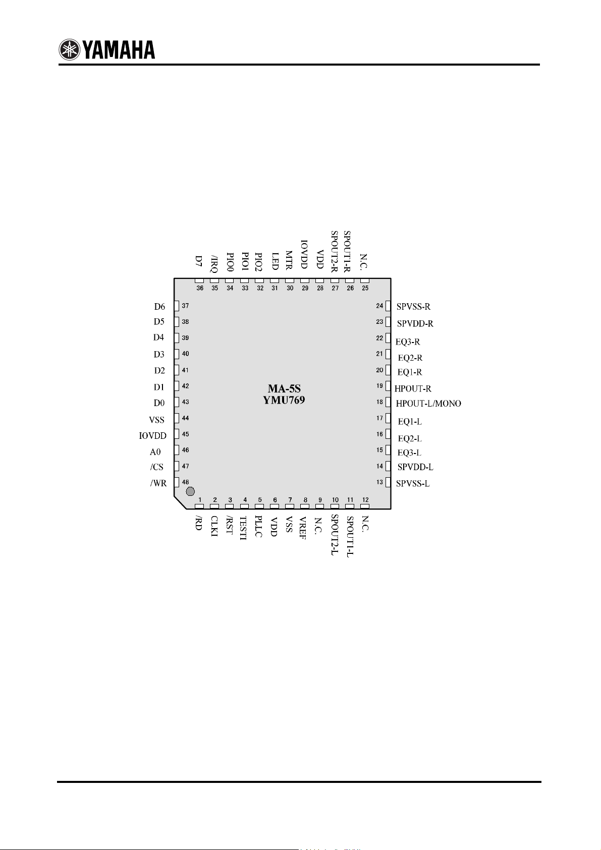
Pin configuration
<48 pins QFN TOP VIEW>
2 Preliminary

YMU769
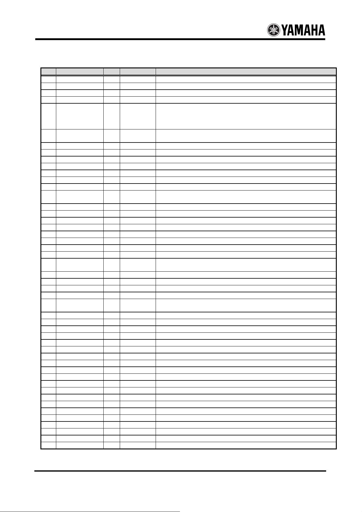
Pin Functions
No. Pin name I/O Power supply Function
1 /RD I IOVDD CPU Interface Read-enable
2 CLKI Ish VDD Pin of input clock (1.5 MHz ~ 20 MHz *Correspondence to TCXO
3 /RST Ish IOVDD Hardware rest input
4 TESTI I IOVDD TEST input (Make sure, connecting with VSS)
Connection of capacitor for built-in PLL
5 PLLC A VDD
6 VDD ─ ─
7 VSS ─ ─ Ground
8 VREF A VDD Analog reference voltage: Connect 0.1 µF capacitor between this pin and VSS.
9 N.C. ─ ─ No Connection (Make sure to use without no connection)
10 SPOUT2-L A SPVDD-L Lch speaker connection pin 2
11 SPOUT1-L A SPVDD-L Lch speaker connection pin 1
12 N.C. ─ ─ No Connection (Make sure to use without no connection)
13 SPVSS-L ─ ─ Analog ground for Lch speaker amplifier
14 SPVDD-L ─ ─
15 EQ3-L A VDD Lch equalizer pin 3
16 EQ2-L A VDD Lch equalizer pin 2
17 EQ1-L A VDD Lch equalizer pin 1
18 HPOUT-L / MONO A VDD Headphone output Lch (it is possible to be MONO output)
19 HPOUT-R A VDD Headphone output Rch.
20 EQ1-R A VDD Rch equalizer pin 1
21 EQ2-R A VDD Rch equalizer pin 2
22 EQ3-R A VDD Rch equalizer pin 3
23 SPVDD-R ─ ─
24 SPVSS-R ─ ─ Analog ground for Rch speaker amplifier.
25 N.C. ─ ─ No Connection (Make sure to use without no connection)
26 SPOUT1-R A SPVDD-R Rch speaker connection pin 1
27 SPOUT2-R A SPVDD-R Rch speaker connection pin 2
28 VDD ─ ─
29 IOVDD ─ ─ Power supply for pins (1.65 ~ VDD)
30 MTR O IOVDD Outside vibrator control pin (Drive Capability = 4mA)
31 LED O IOVDD Outside LED pin (Drive Capability = 4mA)
32 PIO2 I/O IOVDD General-purpose parallel I/O port 2
33 PIO1 I/O IOVDD General-purpose parallel I/O port 1
34 PIO0 I/O IOVDD General-purpose parallel I/O port 0
35 /IRQ O IOVDD Interruption output (Drive Capability = 1mA)
36 D7 I/O IOVDD CPU interface, Data bus 7
37 D6 I/O IOVDD CPU interface, Data bus 6
38 D5 I/O IOVDD CPU interface, Data bus 5
39 D4 I/O IOVDD CPU interface, Data bus 4
40 D3 I/O IOVDD CPU interface, Data bus 3
41 D2 I/O IOVDD CPU interface, Data bus 2
42 D1 I/O IOVDD CPU interface, Data bus 1
43 D0 I/O IOVDD CPU interface, Data bus 0
44 VSS ─ ─ Ground
45 IOVDD ─ ─ Power supply for pin (1.65 ~ VDD)
46 A0 I IOVDD CPU interface, Address signals
47 /CS I IOVDD CPU interface, Chip select
48 /WR 1 IOVDD CPU interface Write-enable
A : Analog pin Ish : Schmitt input
Connect a series connection of 1000 pF capacitor and 3.3 kΩ resistor between this pin
and VSS(*).
(*)Directly connect VSS used here and VSS of 8
Power supply (2.65 ∼ 3.30V)
Connect 0.1 µF and 4.7 µF capacitors between this pin and VSS.
Analog power supply for Lch speaker amplifier (VDD ~ 4.50V)
Connect the condenser 0.1µF and 4.7µF into between main pins and SPVSS-L.
Analog power supply for Rch speaker amplifier. (VDD ~ 4.50 V)
Connect the capacitor 0.1µF and 4.7µF into between main pins and SPVSS-R.
Power supply (2.65 ~ 3.30V) Connecting the condenser 0.1µF and 4.7µF into between
main pins and SPVSS-R.
th
pin.
Preliminary 3

YMU769
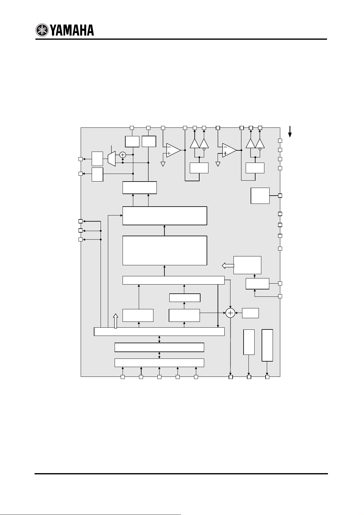
Block Diagram
This section outlines functions of blocks contained in this device and flow of signals.
HPOUT-L
/MONO
HPOUT-R
PIO0
PIO1
PIO2
HP
Vol
HP
Vol
Mono
EQ1-R
EQ1-L
EQ2-R
EQ
EQ
Vol
Vol
VREF
LchRch
16bitDAC
LchRch
DVX arithmetic control
Hybrid
Synthesizer
Control register & SRAM / ROM
EQ3-R
SPOUT1-R
SPOUT2-R
SP
Vol
EQ2-L
VREF
EQ3-L
SPOUT1-L
SP
Vol
Timing
Generator
VREF
PLL
Analog power supply
SPOUT2-L
dedicated to speaker amp
SPVSS-R
SPVDD-R
SPVSS-L
SPVDD-L
VREF
VSS
VDD
IOVDD
TESTI
PLLC
CLKI
write path
Instantaneous
64byte
FIFO
Sequencer
512byte
Delayed write path
FIFO
read path
Instantaneous
Timer
Intermediate register
Interface register
LED control
Vibrator control
CPU Interface
/CS
A0
/RD
/WR
D0 - D7
/IRQ
LED
MTR
4 Preliminary

YMU769
CPU interface
CPU interface is an 8-bit parallel type.
It assumes that a total of 13 pins of 4 control signals (/WR, /RD, /CS, A0 pin), 8 data bus (D0 to D7), and
1 Interrupt pin (/IRQ) are connected to the external CPU.
This block controls the writing and reading of data by the input polarity of control signal.
Interface register
This register is able to access directly from the external CPU. There are 2 bytes spaces.
The latter Intermediate register can be accessed through the Interface register.
Intermediate register
This register is accessed through the Interface register.
The “Control Register” and ROM/SRAM, which describes below, can be accessed through this register.
This register is called “Intermediate register” since this exists in the middle of the Interface register and the
Control register.
In the Intermediate register, there are some registers to control various functions.
Control register, ROM/SRAM
The Control register and ROM/SRAM are accessed from “Instantaneous write register”, “Delayed write
register”, and “Instantaneous read register” in the Intermediate register.
In the Control register, there is a register to control the following synthesizer mainly.
The voice parameter for FM (GM 128 voices + DRUM 40 voices) and Wave data for WT are stored in ROM.
SRAM is used at the download of arbitrary FM voice parameter and Wave data for WT.
Moreover, it is used as storing buffer at the stream playback of PCM/ADPCM.
FIFO
This is an abbreviation of “First In First Out” means the memory which data is read in order of written.
There are 2 paths to write into FIFO in the Intermediate register.
The “Instantaneous write path” is for accessing the Control register and ROM/SRAM immediately, also
“Delayed write path” is for accessing the Control register after managing time through the sequencer.
FIFO size of Instantaneous path is 64-byte, and its size of Delayed path is 512-byte.
Sequencer
This is for interpreting the contents of data which is written into the “Delayed write path”.
Generally, “Music data” is written into the Delayed write path. It interprets the contents of music data and
controls the synthesizer after sequencer, and then plays the music.
Hybrid synthesizer
This device contains a built-in Polyphonic synthesizer that adopts a stereophonic hybrid system that generates
up to 64 tones.
FM synthesizer, WT (Wave Table) synthesizer, Stream playback, and AL (Analog Lite) synthesizer are
available.
DVX Arithmetic control
SD (Stereo Dipole) function that is based on DVX technology makes it possible to create natural stereo sound
even in using adjacent two speakers.
Preliminary 5

YMU769
I/O port section
There are three I/O ports. It is possible to read and write to / from the Intermediate register.
LED, Vibrator control
It is possible to synchronize an LED and vibrator with a play, and to control. A synchronous control to a play
is also possible.
Clock generating bloc k
This device supports a clock input ranging from 1.5 MHz to 20 MHz. (Stop = 0 Hz is possible at power down.)
It is a block to generate a clock which is needed inside of LSI in the PLL.
DAC
It converts digital signals from a synthesizer and a digital audio section into analog signals. The length of a
data is 16bits.
Headphone output
.
This is an amplifier of Stereophonic output for Headphone. The monaural output is also possible.
EQ amplifier
The change of Filter characteristic and Gain is possible by adjusting the resistors and external parts.
Speaker amplifier
The two speakers amplifier, which has a maximum output power of 580 mW at SPVDD_L/_R=3.6V, is
integrated in this device. There is a volume to adjust output level in the first stage of amplifier.
6 Preliminary
 Loading...