

Page 1
UNIVERSAL DOCK for iPod
DRAFT
YDS-12
SERVICE MANUAL
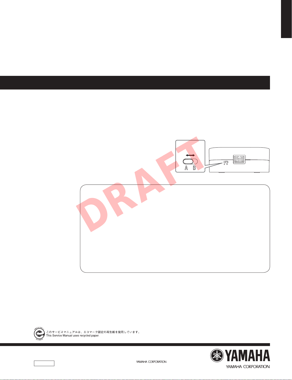
• MODE switch setting
1. When checking operation, the mode switch of this unit properly corresponding MUST be set to the dock-compatible
component connected to this unit.
Position A: For the YDS-12 compatible component (the RX-V367 or later)
Position B: For the Dock-compatible component sold in 2009 or before
2. After repairing is completed, the mode switch of this unit MUST be set to “A” position.
・ モードスイッチの設定
1. 動作チェックする場合、本機に接続した DOCK 対応機器に対応
して本機のモードスイッチを正しくセットしてください。
ポジション A:YDS-12 対応機器(RX-V367 以降)
ポジション B:2009 年度以前に発売された DOCK 対応機器
2. 修理完了後、本機のモードスイッチを “A” の位置にセットして
ください。
MODE switch
モードスイッチ
Rear view /
背面
YDS-12
This manual has been provided for the use of authorized YAMAHA Retailers and their service personnel.
It has been assumed that basic service procedures inherent to the industry, and more specifi cally YAMAHA Products, are already known
and understood by the users, and have therefore not been restated.
WARNING:
IMPORTANT:
The data provided is believed to be accurate and applicable to the unit(s) indicated on the cover. The research, engineering, and service
departments of YAMAHA are continually striving to improve YAMAHA products. Modifications are, therefore, inevitable and
specifi cations are subject to change without notice or obligation to retrofi t. Should any discrepancy appear to exist, please contact the
distributor's Service Division.
WARNING:
IMPORTANT:
Failure to follow appropriate service and safety procedures when servicing this product may result in personal injury,
destruction of expensive components, and failure of the product to perform as specifi ed. For these reasons, we advise
all YAMAHA product owners that any service required should be performed by an authorized YAMAHA Retailer or
the appointed service representative.
The presentation or sale of this manual to any individual or fi rm does not constitute authorization, certifi cation or
recognition of any applicable technical capabilities, or establish a principle-agent relationship of any form.
Static discharges can destroy expensive components. Discharge any static electricity your body may have
accumulated by grounding yourself to the ground buss in the unit (heavy gauge black wires connect to this buss).
Turn the unit OFF during disassembly and part replacement. Recheck all work before you apply power to the unit.
■ CONTENTS
TO SERVICE PERSONNEL ............................................2
FRONT PANEL ...............................................................3
REAR PANELS ...............................................................3
SPECIFICATIONS /
INTERNAL VIEW ............................................................ 4
REPAIR NOTES /
参考仕様
修理上の留意点
.........................................4
.................................. 5
IMPORTANT NOTICE
DISASSEMBLY PROCEDURES /
IC DATA ........................................................................... 7
BLOCK DIAGRAM .......................................................... 8
PRINTED CIRCUIT BOARD ........................................... 9
SCHEMATIC DIAGRAM ................................................10
REPLACEMENT PARTS LIST ...................................... 11
分解手順
...................6
101171
Copyright © 2010 All rights reserved.
This manual is copyrighted by YAMAHA and may not be copied or
redistributed either in print or electronically without permission.
P.O.Box 1, Hamamatsu, Japan
'10.04
Page 2

YDS-12
DRAFT
YDS-12
■ TO SERVICE PERSONNEL
1. Critical Components Information
Components having special characteristics are marked ⚠ and
must be replaced with parts having specifications equal to those
originally installed.
2. Leakage Current Measurement (For 120V Models Only)
When service has been completed, it is imperative to verify
that all exposed conductive surfaces are properly insulated
from supply circuits.
• Meter impedance should be equivalent to 1500 ohms shunted
by 0.15 μF.
WALL
OUTLET
• Leakage current must not exceed 0.5mA.
• Be sure to test for leakage with the AC plug in both polarities.
EQUIPMENT
UNDER TEST
INSULATING
TABLE
WARNING: CHEMICAL CONTENT NOTICE!
This product contains chemicals known to the State of California to cause cancer, or birth defects or other reproductive
harm.
DO NOT PLACE SOLDER, ELECTRICAL/ELECTRONIC OR PLASTIC COMPONENTS IN YOUR MOUTH FOR ANY REASON
WHATSOEVER!
Avoid prolonged, unprotected contact between solder and your skin! When soldering, do not inhale solder fumes or
expose eyes to solder/flux vapor!
If you come in contact with solder or components located inside the enclosure of this product, wash your hands before
handling food.
AC LEAKAGE
TESTER OR
EQUIVALENT
About lead free solder /
All of the P.C.B.s installed in this unit and solder joints are
soldered using the lead free solder.
Among some types of lead free solder currently available,
it is recommended to use one of the following types for
the repair work.
• Sn + Ag + Cu (tin + silver + copper)
• Sn + Cu (tin + copper)
• Sn + Zn + Bi (tin + zinc + bismuth)
Caution:
As the melting point temperature of the lead free solder
is about 30°C to 40°C (50°F to 70°F) higher than that of
the lead solder, be sure to use a soldering iron suitable
to each solder.
無鉛ハンダについて
本機に搭載されているすべての基板およびハンダ付けに
よる接合部は無鉛ハンダでハンダ付けされています。
無鉛ハンダにはいくつかの種類がありますが、修理時に
は下記のような無鉛ハンダの使用を推奨します。
Sn+Ag+Cu(錫+銀+銅)
Sn+Cu(錫 + 銅)
Sn+Zn+Bi(錫 + 亜鉛 + ビスマス)
注意:
無鉛ハンダの融点温度は通常の鉛入りハンダに比べ 30 〜
40℃程度高くなっていますので、それぞれのハンダに合っ
たハンダごてをご使用ください。
2
Page 3
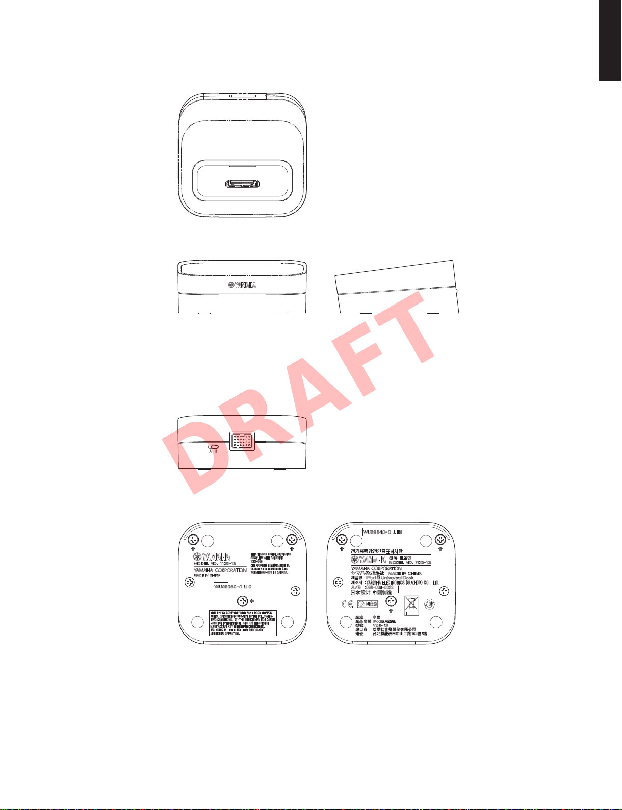
■ FRONT PANEL
DRAFT
Top view
Front view Side view
YDS-12
YDS-12
■ REAR PANELS
Rear view
Bottom view
U, C models R, T, K, A, G, J models
3
Page 4
YDS-12
DRAFT
YDS-12
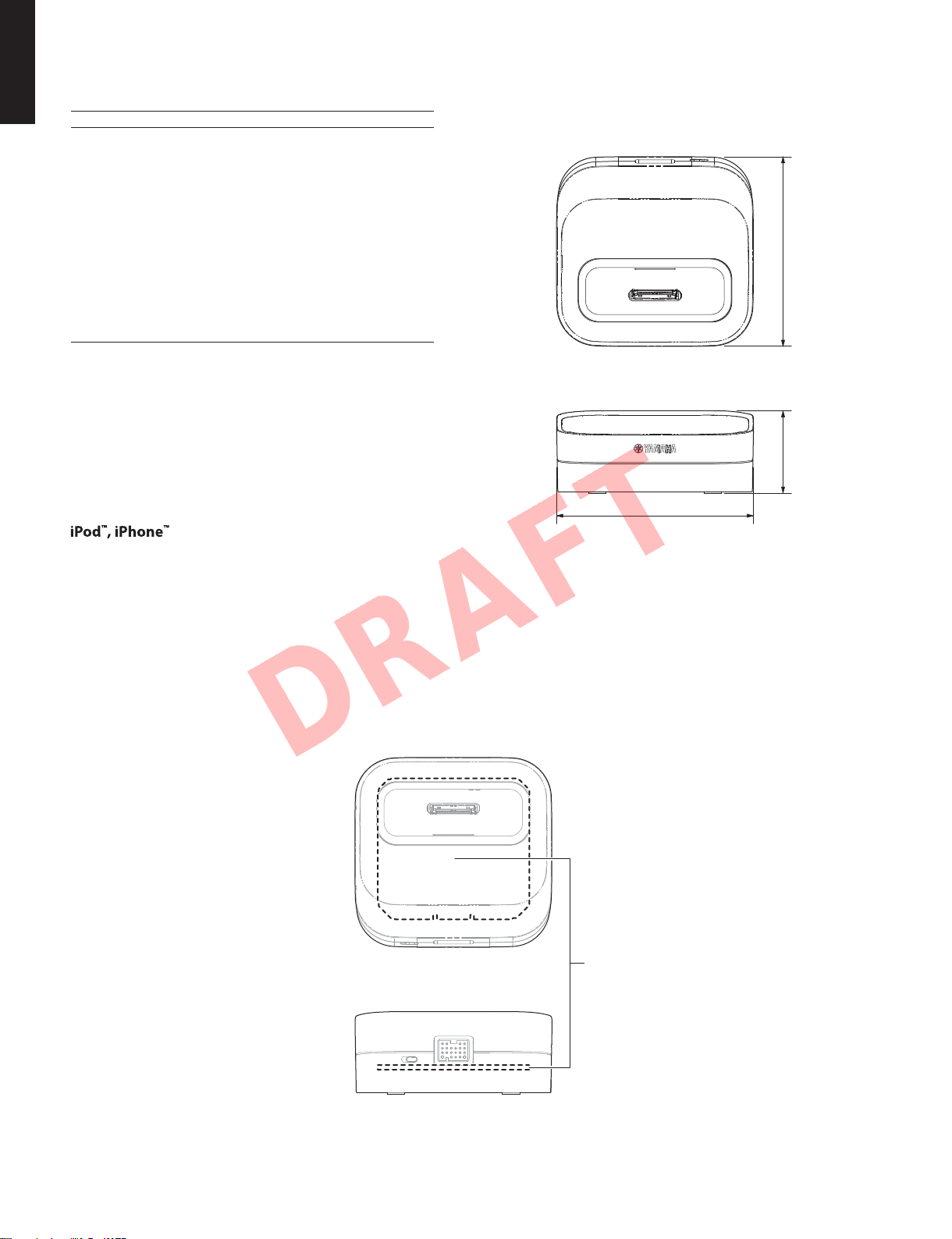
■ SPECIFICATIONS /
■ General /
Dimensions (W x H x D) /
......................................... 89 x 37 x 86 mm (3-1/2" x 1-1/2" x 3-3/8")
Weight / 質量
................................................................................. 160 g (5.64 oz.)
Finish /
U, C, R, T, K, A, G, J models ........................................ Black color
Accessories /
Dock cable (2 m) ..........................................................................x 1
iPod dock adaptor (A type) ..........................................................x 1
iPod dock adaptor (B type) ..........................................................x 1
iPod dock adaptor (C type) ..........................................................x 1
* Specifications are subject to change without notice.
※ 参考仕様および外観は、製品の改良のため予告なく変更すること
があります。
総合
仕上げ
寸法(幅 × 高さ × 奥行き)
付属品
参考仕様
• DIMENSIONS
86 (3-3/8")37 (1-1/2")
U .......................U.S.A. model
C .................Canadian model
R ....................General model
T .................... Chinese model
iPod is a trademark of Apple Inc., registered in the U.S. and other countries.
iPhone is a trademark of Apple Inc.
iPodは、米国およびその他の国々で登録されているApple Inc.の商標です。
iPhoneは、AppleInc.の商標です。
K .....................Korean model
A ................Australian model
G .................European model
J .................. Japanese model
■ INTERNAL VIEW
89 (3-1/2")
Unit: mm (inch)
単位
:mm(インチ)
4
MAIN P.C.B.
Page 5

YDS-12
DRAFT
YDS-12
■ REPAIR NOTES /
1. Supply of replacement parts
None of the components of the MAIN P.C.B. can be
supplied separately.
The MAIN P.C.B. must be replaced as a whole in case
of a failure.
2. Operation check
YDS-12 does not operate by itself.
To check its operation, prepare the Dock-compatible
component (AV receiver, etc. (*1)) and type of the
iPod/iPhone (*2) with this unit.
*1 This unit is not applicable to DVX-C310 (DVR-C310).
*2 The type of iPod/iPhone compatible with this unit:
• iPod (4th Gen/5th Gen/Classic)
• iPod mini
• iPod nano
• iPod Touch
• iPhone
3. MODE switch setting
3-1. When checking operation, the mode switch of
this unit properly corresponding MUST be set to
the dock-compatible component connected to
this unit.
Position A: For the YDS-12 compatible
component (the RX-V367 or later)
Position B: For the Dock-compatible
component sold in 2009 or before
3-2. After repairing is completed, the mode switch of
this unit MUST be set to “A” position.
修理上の留意点
1. サービス部品供給
MAINP.C.B. は、子部品の供給ができません。
故障の場合は、MAINP.C.B. を交換してください。
2. 動作確認
YDS-12 は単独で動作しません。
動作チェックする場合、DOCK 対応機器(AV レシー
バーなど)および、iPod/iPhone(※ 1)を用意して
ください。
※ 1 本機に対応する iPod/iPhone:
・ iPod(4thGen/5thGen/Classic)
・ iPodmini
・ iPodnano
・ iPodTouch
・ iPhone
3. MODE スイッチの設定
3-1. 動作チェックする場合、本機に接続した DOCK
対応機器に対応して本機のモードスイッチを正
しくセットしてください。
ポジション A: YDS-12 対応機器(RX-V367 以
降)
ポジション B: 2009 年度以前に発売された
DOCK 対応機器
3-2. 修理完了後、本機のモードスイッチを “A” の位
置にセットしてください。
5
Page 6

YDS-12
DRAFT
YDS-12
■ DISASSEMBLY PROCEDURES /
1. Removal of MAIN P.C.B.
a. Remove 3 screws (①). (Fig. 1)
* Screws (①) are identified with (⇒) marks. (Fig. 1)
b. Remove the top cabinet.
c. Remove the MAIN P.C.B.. (Fig. 1)
Connector support
コネクターサポート
MAIN P.C.B.
分解手順
1. MAINP.C.B. の外し方
a. ①のネジ 3 本を外します。(Fig.1)
※ ①のネジは(⇒)マークで判別できます。(Fig.1)
b. トップキャビネットを取り外します。
c. MAINP.C.B. を取り外します。(Fig.1)
Top cabinet
トップキャビネット
Knob
ノブ
Bottom View
Boottom cabinet
ボトムキャビネット
①
①
Fig. 1
6
Page 7

■ IC DATA
DRAFT
IC5: R5F21284SNSP (MAIN P.C.B.)
Microprocessor
YDS-12
YDS-12
P3_5
1
TXD1
2
/RESET
3
XOUT
4
VSS
5
XIN
6
VCC
7
MODE
8
RXD1
9
P1_7
10
Pin No. Port Name Function Name I/O Detail of Function
1 P3_5 FET_CTRL O FET control output
2 TXD1 TXD1 O RS232C transmit data output
3 /RESET /RESET I Reset input
4 XOUT XOUT O XOUT clock output
5 VSS VSS I GND
6 XIN XIN I XIN clock input
7 VCC VCC I Power supply input
8 MODE MODE I H : Normal mode, L : Flash rewrite mode
9 RXD1 RXD1 I RS232C receive data input
10 P1_7 DOCK_ID I Dock_ID input (YDS-12/YDS-11)
11 CLK0 CLK0 O SPI_CLK
12 RXD0 RXD0 I SPI_SOMI
13 TXD0 TXD0 O SPI_SIMO
14 P1_3 CP_NRESET O Reset for authentication coprocessor
15 P1_2 ACCPWR_OUT O Accessory_power output to receiver
16 VREF VREF I Reference voltage input
17 P1_1 IPOD_DET_IN I iPod_detect input
18 P1_0 ACCPWR_IN I Accessory_power input from iPod
19 P3_3 SW_SEL_B O RS232C SW select B
20 P3_4 SW_SEL_A O RS232C SW select A
IC5
R5F21284SNSP
P3_4
20
P3_3
19
P1_0
18
P1_1
17
VREF
16
P1_2
15
P1_3
14
TXD0
13
RXD0
12
CLK0
11
7
Page 8

ABCDE
DRAFT
YDS-12
1
■ BLOCK DIAGRAM
8
USB_VBUS
+VCC
+3.3V
IC8
F1
PWR+
1
Regulator
UGND
DGND
8
2
IC6
Authentication IC
(+3.3V, UGND)
3
412
CP_NRESET
14
IC9
13
ACCPWR_IPD
18
Microprocessor
17
(+3.3V, UGND)
4
CB1 iPod connector
IC4
18
19
RX_IPD
TX_IPD
(+3.3V, UGND)
13 14
SPI_SIMO
IC5
29
TX_UC
RX_UC
IC3, 4
Multiplexer
SPI_CLK
SPI_SOMI
111213
10
MODE SWITCH DETECT
15
19
20
A
B
MODE SWITCH
A18K
10K
SW1
B
ACCPWR_RCV
DOCK_ID
TX_RCV
RX_RCV
21
17
CB2 DOCK connector
14
18
5
6
30
IPOD_DET
27
28
21
22
23
29
A/V_RET
AUDIO_L
AUDIO_R
S_Y
S_C
CVBS
AGND
7
8
MAIN
IPOD_DET
AUDIO_GND
r 4FFQBHF→
SCHEMATIC DIAGRAM
4
9
10
12
11
13
15
Page 9

ABCDEFGH I J
DRAFT
1
■ PRINTED CIRCUIT BOARD
FOR INFORMATION ONLY (NO REPLACEMENT COMPONENT PARTS WILL BE AVAILABLE)
MAIN P.C.B. (Side A) MAIN P.C.B. (Side B)
YDS-12
2
3
4
5
MODE switch
161020
IC6
15
11
43
IC7
12
BA
SW1
1
IC8
5
6
2
1
43
DOCK
(To receiver)
CB2
iPod terminal
CB1
1
B
2
A
• Semiconductor Location • Semiconductor Location
Ref no. Location
D1 B3
D2 B3
D3 B3
D7 C5
D8 B5
IC6 B3
IC7 B3
IC8 B3
Q5 B3
201011
IC5
1
16
IC3
1
IC4
1168
9
8
9
4
5
IC9
31
Ref no. Location
D5 F5
IC3 F4
IC4 F4
IC5 F3
IC9 G3
Q3 G5
Q4 G5
POINT A XL1 (Pin 4 of IC5)
6
7
POINT B 1 / IC5 (7 pin, VCC), 2 / IC5 (3 pin, RESET)
1IC5
(VCC)
IC5
(RESET)
2
AC POWER ON
(Connect the power cable)
(VCC)
IC5
(RESET)
AC POWER OFF
(Disconnect the power cable)
1IC5
2
AC POWER OFF
(Disconnect the power cable)
9
Page 10

ABCDEFGH I J
DRAFT
YDS-12
1
■ SCHEMATIC DIAGRAM
FOR INFORMATION ONLY (NO REPLACEMENT COMPONENT PARTS WILL BE AVAILABLE)
POINT B 1 / IC5 (7 pin, VCC), 2 / IC5 (3 pin, RESET)
The voltage is measured with the dock-compatible component.
電圧はDOCK対応機器を接続して測定したものです。
POINT A XL1 (Pin 4 of IC5)
AUTHENTICATION IC
3.4
3.4
3.3
1.7
0
0
3.403.4
3.4
3.4
0
IC6
0
3.4
0
3.4
3.4
0
MICROPROCESSOR
3.4
IC7
3.4
REGULATOR
0
0
BA
(RESET)
5.2
3.4
5.1 3.4
IC8
0
5.2
0
0
0
0
CB2
5.2
0
0
0
0
0
0
0
0
0
0
0
0
3.4
0
0
3.3
3.4
0
2.2
0
2
MULTIPLEXER
0
3.3
3.4
3.4
3.4
3.4
3
3.4
0
3.3
3.4
3.4
3.4
3.4
3.3
0
4
0
0
2.1
2.1
0
0
5
3.4
0
0
CB1
6
To iPod terminal
3.1
3.4
0
0
0
0
0
iPod_L
0
0
0
0
0
0
0
0
0
0
0
0
3.4
0
0
3.4
0
3.4
0
3.4
3.4
3.4
3.4
3.4
IC3IC4
3.4
1
B
2
3.3
3.3
3.303.4
IC5
0
1.7
3.4
3.4
3.4
A
3.4
0
3.4
0
0
0
0
0
3.4
3.4
3.4
3.4
3.4
3.4
IC9
0
3.4
0
1IC5
(VCC)
IC5
2
AC POWER ON
(Connect the power cable)
IC3, 4: TC74VHC153FT
Dual 4-channel multiplexer
A
14
B
2
1C0
6
S0
1C1
5
S1
1C2
4
S2
1C3
3
S3
1G
1
2C0
10
S0
2C1
11
S1
2C2
12
S2
2C3
13
S3
2G
15
To RECEIVER (DOCK)
1IC5
(VCC)
IC5
2
(RESET)
AC POWER OFF
(Disconnect the power cable)
IC6: MFI341S2164
IC digital
S0
S0
S1
S1
S2
S2
S3
S3
Internal address bus
1Y
7
2Y
9
Vcc
Vss
RES
Power-on
reset circuit
On-chip
oscillator
H8/300H
MICROPROCESSOR
System control
Security logic
ROM (112 kbytes)
RAM (4 kbytes)
EEPROM (16 kbytes + 2 kbytes)
Interval timer 1
Interval timer 2
Modular multiplication
coprocessor
NCNCNCNCNC
NC
1
2
P4/IRQ
NC
RES
Vcc
Top view
3
4
5
NCNCNCNCNC
I/O port
RNG
WDT
FMU
Voltage monitoring circuit
Register
(512 bytes)
1617181920
NC
15
14
P3/IRQ
13
P1/IRQ
12
P2/IRQ
11
Vss
9876
10
AC POWER OFF
(Disconnect the power cable)
IC7: R3112Q221A-TR-F
Nch open drain type
P4/IRQ
VDD
P3/IRQ
P2/IRQ
P1/IRQ
Vref
Internal data bus
IC8: R1114Q331D-TR
Low noise 150 mA LDO regulator
VDD
CE
IC9: TC7SH08FU
2-input AND gate
IN B
IN A
GND
PIN CONNECTION DIAGRAMS OF TRANSISTOR, DIODE AND ICS.
MFI341S2164 TC7SH08FU
15
16
20
1
Cathode
11
10
6
5
Anode
R5F21284SNSP
20
1
Cathode
10
Anode
R1114Q331D-TR
R3112Q221A-TR-F
4
RSB6.8S 6.8V1SS400TE61 RB521S-30TE61
Cathode
1
Anode
4
5
2
1
D
G
S
★ All voltages are measured with a 10MΩ/V DC electronic voltmeter.
★ Components having special characteristics are marked ⚠ and must be replaced
with parts having specifications equal to those originally installed.
Vref
Current Limit
1
2
3
3
DTC114EKA2SK3019TL
RD
CD
5
V
CC
OUT Y
4
TC74VHC153FT
16
1
3
1
2
VOUT
GND
1: GND
2: IN
3: OUT
OUT
GND
8
★ Schematic diagram is subject to change without notice.
00
MODE SWITCH
●電圧は、内部抵抗 10MΩの電圧計で測定したものです。
7
●⚠印のある部品は、安全性確保部品を示しています。部品の交換が必要な場合、
パーツリストに記載されている部品を使用してください。
●本回路図は標準回路図です。改良のため予告なく変更することがあります。
10
Page 11

ABCDEFGH I J
DRAFT
1
■ REPLACEMENT PARTS LIST
• OVERALL ASS'Y
YDS-12
Ref No. Part No. Description Remarks Markets
* 1 WU907500 P.C.B. ASS'Y MAIN PCB MAIN
* 5 WU898200 TOP CABINET トップキャビネット
5
2
6
17
8
3
1
4
11
203
A
iPod with color display
(20 GBor 30 GB) or U2 Special Edition
カラーディスプレイ付きiPod
(20GB、30GB)およびU2SpecialEdition
202
6 WR513800 SPRING IPOD スプリングiPod 03
* 7 WU898400 BOTTOM CABINET JRTKAG ボトムキャビネット
* 7 WU920600 BOTTOM CABINET UC ボトムキャビネット
* 8 WV240800 CONNECTOR SUPPORT コネクターサポート
* 11 WU899500 KNOB MODE SWITCH ノブ
15 WF266600 BIND HEAD P-TIGHT SCREW 3x8 MFZN2B3 バインドPタイトネジ 01
16 WF266800 FLAT HEAD B-TIGHT SCREW 3x8 MFZN2B3 皿Bタイトネジ
17 WF267600 BIND HEAD P-TIGHT SCREW 2x6 MFZN2B3 バインドPタイトネジ 01
18 WG595300 NONSKID PAD D8 t=1 滑止パッド
ACCESSORIES 付属品
* 202 WU805500 DOCK CABLE 21P 2m 1pc LLM2118-2000 DOCKケーブル
* 203 WR558200 IPOD DOCK ADAPTOR Black Atype 1pc
* 204 WR558400 IPOD DOCK ADAPTOR Black Btype 1pc
* 205 WR558100 IPOD DOCK ADAPTOR Black Ctype 1pc
部 品 名
iPod DOCKアダプター
iPod DOCKアダプター
iPod DOCKアダプター
ランク
01
01
01
7
5
18
15
16
6
18
15
* The mark ( , , or ) is shown on the back of each iPod dock adapter.
B CA
、 、 はiPodDockアダプターの裏面に表示されています。
204
205
B CA
B
iPod with color display
(40 GB or 60 GB) or iPod (40 GB)
iPod(40GB)、カラーディスプレイ付き
iPod(40GBおよび60GB)
C
iPod mini (4 GB or 6 GB)
iPodmini(4GBおよび6GB)
7
✻ New Parts
✻ New Parts
*新規部品
*新規部品
11
Page 12

YDS-12
DRAFT
 Loading...