

Page 1

YDA163C
D-515D
DIGITAL INPUT STEREO 20W DIGITAL AUDIO POWER AMPLIFIER
■ Overview
YDA163C(D-515D) is a high-performance digital audio amplifier IC that delivers up to 20W×2ch, which
*1)
has a digital audio interface, and is capable of operating at a supply voltage ranging from 5V
YDA163C, having Yamaha original “Pure Pulse Direct Speaker Drive Circuit,” allows a speaker to be
directly connected to the output. In addition, this amplifier is insusceptible to supply voltage fluctuation
because of a feedback-type digital amplifier, and have the feature with high power supply noise tolerance.
As a result, power supply can be simplified and allowing a simple amplifier system with less external
components to be configured. YDA163C has the following functions: power limit function, pop noise
reduction function, overcurrent protection function for speaker output pins, internal overtemperature
protection function, under voltage lockout, and DC detection function. And, YDA163C supports power
MUTEN
SLEEPN
PLIMIT
MONO
CKMOD
HOPP
MCK
SCLK
LRCLK
SDATA
L
=8Ω, Mode:7).
YDA163C
Digital Control DEM DAC
Control
I/F
Digital I/F
32kHz
44.1kHz
48kHz
VREF
DC Cut Filter
Power Limitter
3.3V
DVDD
10Hz
2.5W to 15W
8Levels
Volume
Over Sampling
x4 FS
+6dB
-6dB
0dB
3.4V Regulator
Lch.
Dynamic
Element
Matching
(16 Levels)
Rch.
AVSS DVSS
5V*1~ 18V
PVDDxx
Class-
D
Protection
OCP
OTP
DCOP
UVLO
Class-
D
r
t
n
o
C
e
t
Mu
PVSSx
REFA
Lch
4~Ω
PROTN
Rch
l
o
4~Ω
limit setting of 3W (R
GAIN[1:0]
<YDA163C Overview>
(Note) *1: When operating at less than 8V (V
), an 8Ω or more load must be used.
DDP
to 18V.
YDA163C CATALOG
CATALOG No. LSI-4DA163C20
2011.1
Page 2

■ Features YDA163C
■ Features
・Supply Voltage Range V
V
DDP
DD
*1)
5V
to 18V
3.0V to 3.6V
・Input Digital Audio Interface (Stereo)
Sampling Frequency: 32kHz, 44.1kHz, 48kHz
Left-justified, MSB first, 1-bit delay, Digital Audio Data 24-bits
・Max. Instantaneous Output 15W×2ch (V
10W×2ch (V
20W×2ch (V
*2)
・Max. Continuous Output 15W
×2ch (V
*2)
10W
×2ch (V
・Distortion Ratio (THD+N) 0.05% (V
・Residual Noise 50μVrms (V
・S/N Ratio 105dB (V
・Efficiency 92% (V
・Channel Separation 80 dB (V
・Power Limit Function (Supports power limit setting of 3W (R
=15V, RL=8Ω, THD+N=10%)
DDP
=12V, RL=8Ω, THD+N=10%)
DDP
=14V, RL=4Ω, THD+N=10%)
DDP
=15V, RL=8Ω, Ta=70 ºC, 4-layer Board)
DDP
=12V, RL=8Ω, Ta=70 ºC, 4-layer Board)
DDP
=12V, RL=8Ω, Po=4.5W, 1kHz)
DDP
=12V, RL=8Ω)
DDP
=12V, RL=8Ω)
DDP
=12V, RL=8Ω, Po=10W)
DDP
=12V, RL=8Ω, 1kHz)
DDP
=8Ω, Mode:7))
L
・Gain Setting Function (3steps: +6dB/0dB/-6dB)
・Stereo/Monaural Switching Function
・Output Mute Function (Quick Mute/Quick Start)
・Sleep Function
・Pop Noise Reduction Function
・Carrier Clock Frequency Hopping Function
・Overcurrent Protection Function (OCP)
・Over Temperature Protection Function (OTP)
・Under voltage lockout (UVLO)
・DC Detection Function (DCDET)
・Clock Detection Function (CKDET)
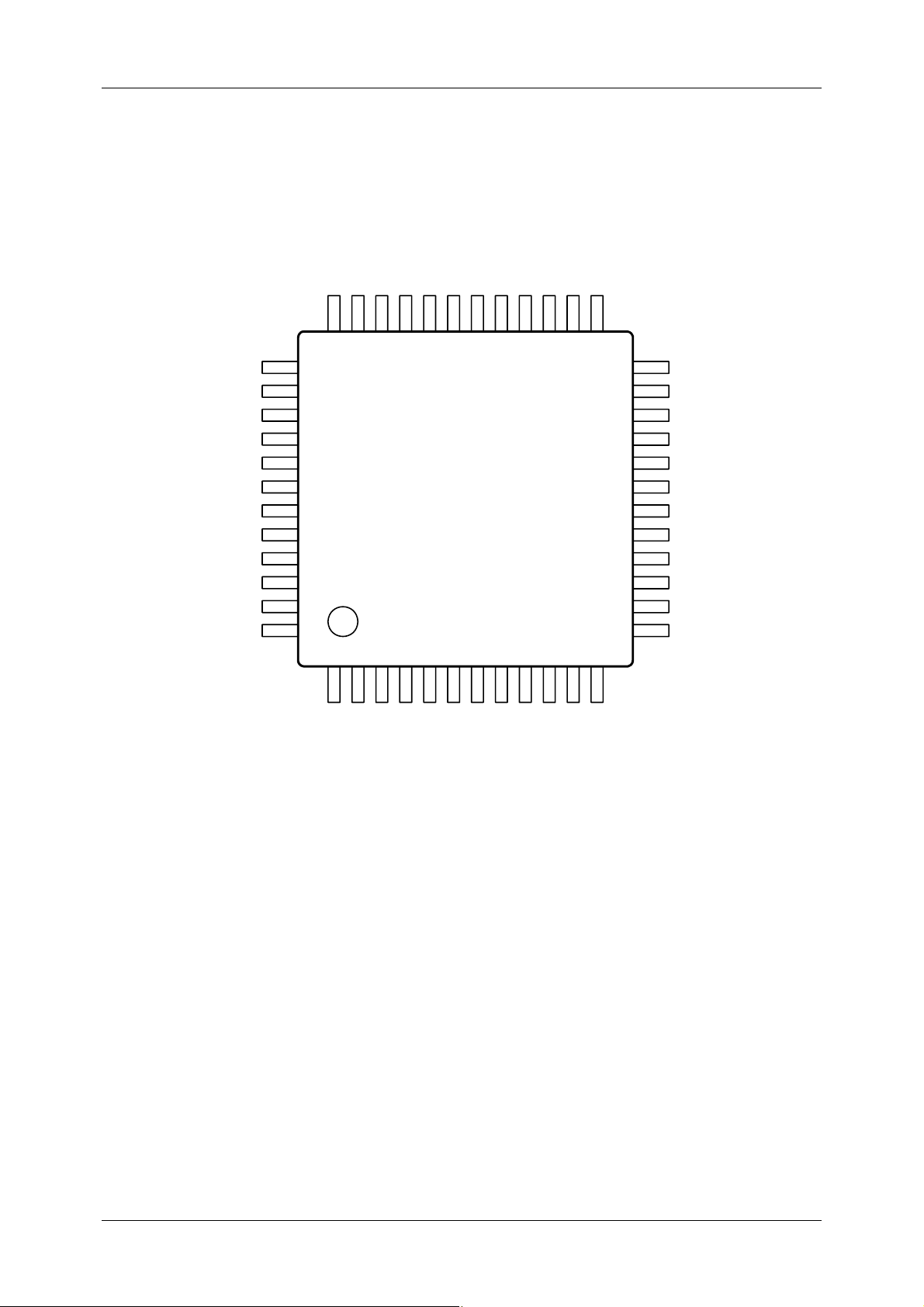
・Package Lead-free 48-pin Plastic SQFP (Stage die pad) : YDA163C-SZ
(Note) *1: When operating at less than 8V (V
), an 8Ω or more load must be used.
DDP
*2: These values are based on evaluations on a Yamaha's PCB board implementation.
Please refer to Power Dissipation (Note) *1 on page 6.
4DA163C20 2
Page 3
■ Pin Assignments YDA163C
■ Pin Assignments
PVSSL
PVDDML
PVDDML
OUTML
OUTML
PVSSL
PVSSL
OUTPL
OUTPL
PVDDPL
PVDDPL
PVSSL
37
38
39
40
41
42
43
44
45
46
47
48
N.C.
36
1
N.C.
MONO
35
2
N.C.
GAIN1
GAIN0
34
33
3
4
VREF
AVSS
CKMOD
32
5
REFA
MUTEN
PROTN
31
30
7
6
MCK
DVDD
SLEEPN
PLIMIT
29
28
8
9
SCLK
SDATA
HOPP
27
10
LRCLK
N.C.
N.C.
26
25
11
12
N.C.
DVSS
24
23
22
21
20
19
18
17
16
15
14
13
PVSSR
PVDDMR
PVDDMR
OUTMR
OUTMR
PVSSR
PVSSR
OUTPR
OUTPR
PVDDPR
PVDDPR
PVSSR
< 48 pin SQFP Top View >
4DA163C20 3
Page 4

■ Pin Descriptions YDA163C
■ Pin Descriptions
No. Name I/O
1 N.C. - No Connection pin. This pin must be left open or connected to GND.
2 N.C. - No Connection pin. This pin must be left open or connected to GND.
3 AVSS GND Analog GND
4 VREF AO Analog Reference Voltage Output
5 REFA AO Internal Regulator Output
6 DVDD DVDD power Digital Power
7 MCK I Master Clock Input Pin
8 SDATA I Audio Data Input Pin
9 SCLK I Bit Clock Input Pin
10 LRCLK I Word Clock Input Pin
11 DVSS GND Digital GND
12 N.C. - No Connection pin. This pin must be left open or connected to GND.
13 PVSSR GND GND for the digital amplifier output (Rch)
14 PVDDPR PVDD power Power for the digital amplifier output (Rch+)
15 PVDDPR PVDD power Power for the digital amplifier output (Rch+)
16 OUTPR O Digital Amplifier Output (Rch+)
17 OUTPR O Digital Amplifier Output (Rch+)
18 PVSSR GND GND for the digital amplifier output (Rch)
19 PVSSR GND GND for the digital amplifier output (Rch)
20 OUTMR O Digital Amplifier Output (Rch-)
21 OUTMR O Digital Amplifier Output (Rch-)
22 PVDDMR PVDD power Power for the digital amplifier output (Rch-)
23 PVDDMR PVDD power Power for the digital amplifier output (Rch-)
24 PVSSR GND GND for the digital amplifier output (Rch)
25 N.C. - No Connection pin. This pin must be left open or connected to GND.
26 N.C. - No Connection pin. This pin must be left open or connected to GND.
27 HOPP I PWM Carrier Frequency Hopping setting pin
28 PLIMIT I Power Limit setting pin
29 SLEEPN I Sleep Reset pin
30 PROTN O/D Error Flag Output pin
31 MUTEN I Mute pin
32 CKMOD I Clock Mode setting pin
33 GAIN0 I Gain setting pin 0
34 GAIN1 I Gain setting pin 1
35 MONO I Stereo/Mono setting pin
36 N.C. - No Connection pin. This pin must be left open or connected to GND.
37 PVSSL GND GND for the digital amplifier output (Lch)
38 PVDDML PVDD power Power for the digital amplifier output (Lch-)
39 PVDDML PVDD power Power for the digital amplifier output (Lch-)
40 OUTML O Digital Amplifier Output (Lch-)
41 OUTML O Digital Amplifier Output (Lch-)
42 PVSSL GND GND for the digital amplifier output (Lch)
43 PVSSL GND GND for the digital amplifier output (Lch)
44 OUTPL O Digital Amplifier Output (Lch+)
45 OUTPL O Digital Amplifier Output (Lch+)
46 PVDDPL PVDD power Power for the digital amplifier output (Lch+)
47 PVDDPL PVDD power Power for the digital amplifier output (Lch+)
48 PVSSL GND GND for the digital amplifier output (Lch)
*1)
Function
*2)
(Note) *1: I: Input pin, O: Output pin, A: Analog pin, O/D: Open-Drain output pin
PVDD power pins should be connected each other on the board. Likewise, GND pins should be
also connected each other on it.
*2: A voltage for supplying SLEEP pin with H level should be applied not from REFA pin output but
from an external power supply.
4DA163C20 4
Page 5

■ Block Diagram YDA163C
■ Block Diagram
SLEEPN
CKMOD
GAIN[1:0]
MUTEN
MONO
PROTN
HOPP
SCLK
SDATA
LRCLK
MCK
PLIMIT
AVSS
REFA
VREF
DVDD
DVSS
Control
Digital
Audio
I/F
PLIMIT
Set
Regulator
VREF
SLEEPN
DCDET
CKDET
OTP
OCP
UVLO
DC cut Filter
Over Sampling Filter
Power Limiter
Lch
Feed Back
PWM
Amp
DAC
Noise Shaper
Rch
PWM
Amp
Level
Shift
Feed Back
Feed Back
Level
Shift
Feed Back
YDA163C
Logic
Logic
PVDDPL
OUTPL
PVSSL
OUTML
PVDDML
PVDDPR
OUTPR
PVSSR
OUTMR
PVDDMR
< YDA163C Block Diagram >
4DA163C20 5
Page 6

■ Electrical Characteristics YDA163C
■ Electrical Characteristics
● Absolute Maximum Ratings
Item Symbol Min. Max. Unit
*1)
Power Supply pin (PVDD) Voltage Range V
Power Supply pin (DVDD) Voltage Range V
Input Pin Voltage Range
*2)
HOPP, HORL Pins Voltage Range V
V
DDP
DD
IN1
IN2
–0.3 21.6 V
–0.3 4.6 V
–0.3 4.6 V
–0.3 VDD+0.3 V
Junction Temperature Tjmax – 150 ºC
Storage Temperature T
V
≧8V
Speaker Impedance
DDP
<8V
V
DDP
R
R
STG
LS
LS
–40 150 ºC
3.2 – Ω
6.4 – Ω
(Note) *1: Absolute Maximum Ratings are values which must not be exceeded to guarantee device reliability
and life, and when using a device in excess of the ratings for even a moment, it may immediately
cause damage to the device or may significantly deteriorate its reliability.
*2: Input Pins: MUTEN, MCK, SCLK, LRCLK, SDATA, CKMOD, GAIN[1:0], SLEEPN, and PLIMIT
● Power Dissipation
Item Symbol Condition Min. Max. Unit
*1)
*1)
*1)
*2)
*2)
*2)
Power Dissipation
4-layer
board
2-layer
board
P
D25
P
D70
P
D85
P
D25
P
D70
P
D85
Thermal resistance θja =19℃/W
Thermal resistance θja =33.6℃/W
TA=25℃
TA=70℃
=85℃
T
A
TA=25℃
TA=70℃
=85℃
T
A
– 6.51
– 4.21
– 3.4
– 3.72
– 2.38
– 1.93
W
W
W
W
W
W
(Note) *1: Board layer: 4 layers, Size: 136[mm]× 85[mm], copper foil thickness: 35[μm],
Copper foil ratio: 379%, Exposed Stage: Soldered to the board,
Thermal Via (φ0.5mm): 25(5×5) from the exposed stage side to internal layers (VSS layer) and B
side
*2: Board layer: 2 layers, Size: 136[mm] × 85[mm], copper foil thickness: 35[μm],
Copper foil ratio: 187%, Exposed Stage: Soldered to the board,
Thermal Via (φ0.5mm) : 25(5×5) from the exposed stage side to B side
4DA163C20 6
Page 7

■ Electrical Characteristics YDA163C
● Recommended Operating Conditions
Item Symbol Condition Min. Max. Unit
Supply Voltage (PVDD) V
Supply Voltage (DVDD) V
Digital pins
*1)
Input Voltage H level V
SLEEPN pin Input Voltage H level V
Ambient Operating Temperature T
DDP
DD
IN
IN
A
*2)
5
– 18 V
3.0 3.3 3.6 V
2.0 3.3 3.6 V
2.2 3.3 3.6 V
–40 25 85 ºC
(Note) *1: Digital Pins: MUTEN, MCK, SCLK, LRCLK, SDATA, CKMOD, GAIN[1:0], HOPP, and MONO
*2: When operating at less than 8V (V
), an 8Ω or more load must be used.
DDP
● DC characteristics
(V
= 5V to 18V, V
DDP
= 3.0V to 3.6V, V
DD
= 0V, TA = –40℃ to 85℃, unless otherwise specified)
SS
Item Symbol Condition Min. Ty p. Max. Unit
PVDD pin
Startup Threshold Voltage V
Shutdown Threshold Voltage V
DVDD pin
Startup Threshold Voltage V
Shutdown Threshold Voltage V
Input Voltage H level V
Digital pins
*1)
Input Voltage L level V
Input Impedance R
Input Voltage H level V
SLEEPN pin
Input Voltage L level V
Input Impedance R
PROTN pin Output Voltage V
REFA pin Output Voltage V
VREF pin Output Voltage V
at idling state I
PVDD
Current
Consumption
at power-down state
(SLEEPN=L)
at mute state
I
I
(MUTEN=L)
HUVLH
HUVLL
LUVLH
LUVLL
IH
IL
IN_D
IH
IL
IN_D
OL
REFA
REF
DDPP
DDPS
DDPM
– – 4.3 – V
– – 4.15 – V
– – 2.0 – V
– – 2.0 – V
– 2.0 – – V
– – – 0.8 V
– 3.3 – – MΩ
– 2.2 – – V
– – – 0.5 V
– 3.3 – – MΩ
IOL=2mA – – 0.4 V
– – 3.4 – V
– – V
V
=12V,
DDP
– 22 – mA
/2 – V
REFA
No load
V
=12V,
DDP
No load, TA = 25℃
V
=12V,
DDP
– 7 – μA
– 12 – mA
No load
DVDD
Current
Consumption
at idling state I
at power-down state
(SLEEPN=L)
at mute state
(MUTEN=L)
DDP
I
DDS
I
DDM
VDD =3.3V – 9 – mA
VDD =3.3V,
T
= 25℃
A
– 45 – μA
VDD =3.3V – 9 – mA
(Note) *1: Digital Pins: MUTEN, MCK, SCLK, LRCLK, SDATA, CKMOD, GAIN[1:0], HOPP, and MONO
4DA163C20 7
Page 8

■ Electrical Characteristics YDA163C
● AC Characteristics
(V
= 5V to 18V, V
DDP
MCK
Input Frequency
= 3.0V to 3.6V, V
DD
= 0V, TA = –40℃ to 85℃, unless otherwise specified)
SS
Item Symbol Min. Typ. Max. Unit
11.290
12.288
*1)
f
MCK
Typ × 0.95
16.384
Typ × 1.05 MHz
22.579
24.576
Duty MCK
Input Frequency f
SCLK
Rise Time t
Fall Time t
Input Frequency f
LRCLK
Setup Time t
Hold Time t
Rise Time t
Fall Time t
Setup Time t
Hold Time t
SDATA
Rise Time t
Fall Time t
MUTE Recovery Time (fs=48kHz) t
SCLK
SCU
SCD
S
LRS
LRH
LRU
LRD
SDS
SDH
SDU
SDD
mrcv
DUT
40
-
-
64 × fs
- -
- -
32
-
44.1
48
10
10
- -
- -
- -
- -
10
10
- -
- -
- -
- -
-
5.3
60 %
- -
15 ns
15 ns
-
kHz
ns
ns
15 ns
15 ns
ns
ns
15 ns
15 ns
-
ms
(Note) *1: Refer to YDA163C Application manual “Table 6-1 Carrier Clock Frequency” at page 16
for the MCK Input Frequency.
MCK
DUT
1/f
MCK
MCK
V
IH
V
IL
< Master Clock Input Timing >
4DA163C20 8
Page 9

■ Electrical Characteristics YDA163C
SCLK
t
SCU
V
IH
V
IL
t
SCD
V
SDATA
LRCLK
t
SDS
t
SDH
IH
V
IL
t
SDU,tSDD
t
LRU,tLRD
V
IH
V
IL
t
LRS
t
LRH
< Digital Audio Interface Timing >
4DA163C20 9
Page 10

■ Electrical Characteristics YDA163C
● Analog Characteristics
(V
= 12V, V
DDP
Maximum Instantaneous Output
Maximum Continuous Output
Total Harmonic Distortion
Residual Noise
S/N Ratio
Channel Separation (L vs R)
*1)
PSRR
Maximum Efficiency
Output Offset Voltage (Stereo)
Frequency Characteristics f
(Note) All analog characteristics were measured by using Yamaha evaluation board. Depending upon pattern
*1)
= 3.3V, V
DD
= 0V, TA= 25℃, RL = 8Ω, unless otherwise specified)
SS
Item Symbol Condition Min. Typ. Max. Unit
V
=14V, RL=4Ω,
Stereo Po
Monaural Po
T
Stereo Po
Monaural Po
A
T
A
T
A
DDP
THD+N=10%
=15V, RL=8Ω,
V
DDP
THD+N=10%
=15V, RL=4Ω,
V
DDP
THD+N=10%
V
=15V, RL=8Ω,
DDP
=70℃, 4-layer board
=12V, RL=8Ω,
V
DDP
=70℃, 4-layer board
=15V, RL=4Ω,
V
DDP
=70℃, 4-layer board
– 20 – W
– 15 – W
– 25 – W
– 15 – W
– 10 – W
– 25 – W
Stereo THD+N RL=8Ω, Po=4.5W – 0.05 – %
=8Ω, Po=4.5W – 0.05 – %
L
=8Ω,
R
L
A-Weighted Filter
=8Ω,
R
L
A-Weighted Filter
=8Ω,
R
L
A-Weighted Filter
=8Ω,
R
L
A-Weighted Filter
PVDD applied,
Vripple=200mV,f=1kHz
PVDD applied,
Vripple=200mV,f=1kHz
– 50 – μVrms
– 50 – μVrms
– 105 – dB
– 105 – dB
– 60 – dB
– 60 – dB
RL=8Ω, Po=10W – 92 – %
R
=4Ω, Po=15W – 88 – %
L
RL=8Ω, Po=10W – 93 – %
R
=4Ω, Po=20W – 93 – %
L
*1)
Monaural THD+N R
Stereo Vn
Monaural Vn
Stereo SNR
Monaural SNR
*1)
CS RL=8Ω,1kHz – 80 – dB
Stereo PSRR
Monaural PSRR
Stereo η
Monaural η
*2)
Vo – – 2 6 mV
20Hz –1 0 1 dB
20kHz –3 0 1 dB
layout etc., its characteristics may vary.
*1: Except the case of HOPP=H
*2: An offset voltage is represented by taking typ. as σ and max. as 3σ.
4DA163C20 10
Page 11

■ Package Information YDA163C
■ Package Information
4DA163C20 11
Page 12

YDA163C
PRECAUTIONS AND INSTRUCTIONS FOR SAFETY
WARNI NG
Do not use the device under stresses beyond those listed in Absolute Maximum Ratings.
Such stresses may become causes of breakdown, damages, or deterioration, causing explosion
Prohibited
Prohibited
Prohibited
Instructions
or ignition, and this may lead to fire or personal injury.
Do not mount the device reversely or improperly and also do not connect a supply voltage in
wrong polarity. Otherwise, this may cause current and/or power-consumption to exceed the
absolute maximum ratings, causing personal injury due to explosion or ignition as well as causing
breakdown, damages, or deterioration.
And, do not use the device again that has been improperly mounted and powered once.
Do not short between pins.
In particular, when different power supply pins, such as between high-voltage and low-voltage
pins, are shorted, smoke, fire, or explosion may take place.
As to devices capable of generating sound from its speaker outputs, please design with safety of
your products and system in mind, such as the consequences of unusual speaker output due to a
malfunction or failure. A speaker dissipates heat in a voice-coil by air flow accompanying vibration
of a diaphragm. When a DC signal (several Hz or less) is input due to device failure, heat
dissipation characteristics degrade rapidly, thereby leading to voice-coil burnout, smoking or
ignition of the speaker even if it is used within the rated input value.
Prohibited
Instructions
Instructions
Instructions
Instructions
Instructions
Instructions
CAUTION
Do not use Yamaha products in close proximity to burning materials, combustible substances, or
inflammable materials, in order to prevent the spread of the fire caused by Yamaha products, and
to prevent the smoke or fire of Yamaha products due to peripheral components.
Generally, semiconductor products may malfunction and break down due to aging, degradation,
etc. It is the responsibility of the designer to take actions such as safety design of products and
the entire system and also fail-safe design according to applications, so as not to cause property
damage and/or bodily injury due to malfunction and/or failure of semiconductor products.
The built-in DSP may output the maximum amplitude waveform suddenly due to malfunction from
disturbances etc. and this may cause damage to headphones, external amplifiers, and human
body (the ear). Please pay attention to safety measures for device malfunction and failure both in
product and system design.
As semiconductor devices are not nonflammable, overcurrent or failure may cause smoke or fire.
Therefore, products should be designed with safety in mind such as using overcurrent protection
circuits to control the amount of current during operation and to shut off on failure.
Products should be designed with fail safe in mind in case of malfunction of the built-in protection
circuits. Note that the built-in protection circuits such as overcurrent protection circuit and
high-temperature protection circuit do not always protect the internal circuits. In some cases,
depending on usage or situations, such protection circuit may not work properly or the device
itself may break down before the protection circuit kicks in.
Use a robust power supply.
The use of an unrobust power supply may lead to malfunctions of the protection circuit, causing
device breakdown, personal injury due to explosion, or smoke or fire.
Product's housing should be designed with the considerations of short-circuiting between pins of
the mounted device due to foreign conductive substances (such as metal pins etc.). Moreover,
the housing should be designed with spatter prevention etc. due to explosion or burning.
Otherwise, the spattered substance may cause bodily injury.
The device may be heated to a high temperature due to internal heat generation during
operation. Therefore, please take care not to touch an operating device directly.
Instructions
4DA163C20 12
v02
Page 13

 Loading...