

Page 1
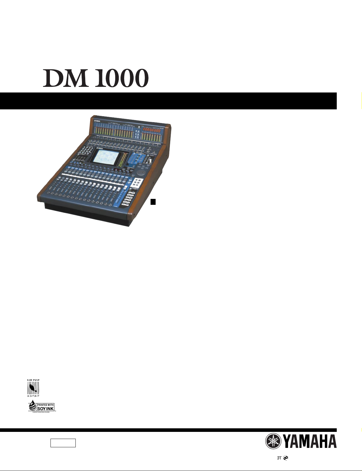
DM1000/MB1000/SP1000
DIGITAL PRODUCTION CONSOLE/
PEAK METER BRIDGE/WOODEN SIDE PANELS
/MB1000/SP1000
SERVICE MANUAL
このサービスマニュアルはエコパルプ
(ECF:無塩素系漂白パルプ)を使用しています。
このサービスマニュアルは大豆油
インクで印刷しています。
This document is printed on chlorine free (ECF) paper with soy ink.
CONTENTS
SPECIFICATIONS ................................................... 4
DIMENSIONS .......................................................... 13
PANEL LAYOUT .................................. 14
CIRCUIT BOARD LAYOUT ............... 23
DISASSEMBLY PROCEDURE ............................ 28
INSTALLING AN OPTIONAL CARD
(オプションカードの取り付け)
LSI PIN DESCRIPTION ................................ 47
IC BLOCK DIAGRAM .................................. 58
CIRCUIT BOARDS ....................................... 65
INSPECTIONS ...................................................103/109
DM1000/MB1000 SERVICE CHECK PROGRAM
(DM1000/MB1000サービス検査プログラム)
MB1000 TEST PROGRAM
(MB1000テストプログラム)
INITIALIZING THE DM1000 ................. 145
TRANSMITTING PARAMETER SETTINGS VIA MIDI (BULK DUMP)
(内部設定をMIDI経由で出力(バルクダンプ機能))
CHECKING THE BATTERY AND THE SYSTEM VERSION
(バッテリーの残量やシステムのバージョンの確認)
CALIBRATING THE FADERS
(フェーダーのキャリブレーション)
MIDI DATA FORMAT ............... 151
MIDI IMPLEMENTATION CHART
(MIDIインプリメンテーションチャート)
PARTS LIST
BLOCK DIAGRAM
OVERALL CONNECTOR CIRCUIT DIAGRAM
(総コネクタ接続回路図)
CIRCUIT DIAGRAM
(目次)
(
総合仕様
(寸法図)
(パネルレイアウト)
(ICブロック図)
(シート基板図)
(検査)
(MIDIデータフォーマット)
(ブロックダイアグラム)
(回路図)
)
(ユニットレイアウト)
(分解手順)
............................................ 46
(LSI端子機能表)
........................................143/144
(DM1000の初期化)
..................115/129
....146/148
.......... 150
................................... 150
............................ 166
011681
PA
DM1000: 200303-600000
MB1000: 200303-105000
SP1000: 200303-35000
HAMAMATSU, JAPAN
1.329K-6554 Printed in Japan ’03.03
1
Page 2
DM1000/MB1000/SP1000
This manual has been provided for the use of authorized Yamaha Retailers and their service personnel. It has been assumed
that basic service procedures inherent to the industry, and more specifically Yamaha Products, are already known and understood by the users, and have therefore not been restated.
WARNING : Failure to follow appropriate service and safety procedures when servicing this product may result in per-
IMPORTANT : This presentation or sale of this manual to any individual or firm does not constitute authorization certifi-
The data provided is belived to be accurate and applicable to the unit(s) indicated on the cover. The research engineering, and
service departments of Yamaha are continually striving to improve Yamaha products. Modifications are, therefore, inevitable
and changes in specification are subject to change without notice or obligation to retrofit. Should any discrepancy appear to
exist, please contact the distributor’s Service Division.
WARNING : Static discharges can destroy expensive components. Discharge any static electricity your body may have
IMPORTANT : Turn the unit OFF during disassembly and parts replacement. Recheck all work before you apply power
IMPORTANT NOTICE
sonal injury, destruction of expensive components and failure of the product to perform as specified. For
these reasons, we advise all Yamaha product owners that all service required should be performed by an
authorized Yamaha Retailer or the appointed service representative.
cation, recognition of any applicable technical capabilities, or establish a principal-agent relationship of
any form.
accumulated by grounding yourself to the ground bus in the unit (heavy gauge black wires connect to
this bus.)
to the unit.
WARNING: CHEMICAL CONTENT NOTICE!
The solder used in the production of this product contains LEAD. In addition, other electrical/electronic and/or plastic (Where
applicable) components may also contain traces of chemicals found by the California Health and Welfare Agency (and possibly
other entities) to cause cancer and/or birth defects or other reproductive harm.
DO NOT PLACE SOLDER, ELECTRICAL/ELECTRONIC OR PLASTIC COMPONENTS IN YOUR MOUTH FOR ANY REASON WHAT
SO EVER!
Avoid prolonged, unprotected contact between solder and your skin! When soldering, do not inhale solder fumes or expose
eyes to solder/flux vapor!
If you come in contact with solder or components located inside the enclosure of this product, wash your hands before handling
food.
WARNING: THIS APPARATUS MUST BE EARTHED
IMPORTANT
THE WIRES IN THIS MAINS LEAD ARE COLOURED IN
ACCORDANCE WITH THE FOLLOWING CODE:
GREEN-AND-YELLOW : EARTH
BLUE : NEUTRAL
BROWN : LIVE
As the colours of the wires in the mains lead of this apparatus may
not correspond with the coloured markings identifying the terminals in
your plug, proceed as follows:
The wire which is coloured GREEN and YELLOW must be
connected to the terminal in the plug which is marked by the letter E
or by the safety earth symbol or coloured GREEN and YELLOW.
The wire which is coloured BLUE must be connected to the terminal
which is marked with the letter N or coloured BLACK.
The wire which is coloured BROWN must be connected to the
terminal which is marked with the letter L or coloured RED.
* This applies only to products distributed by YAMAHA KEMBLE
MUSIC (U.K.) LTD.
WARNING
Components having special characteristics are marked and must be replaced with parts having specification equal to those
originally installed.
印の商品は、安全を維持するために重要な部品です。交換する場合は、安全のために必ず指定の部品をご使用下さい。
2
Page 3
DM1000/MB1000/SP1000
LITHIUM BATTER Y HANDLING
This product uses a lithium battery for memory back-up.
WARNING : Lithium batteries are dangerous because they can be exploded by improper handling. Observe the following pre-
Leave lithium battery replacement to qualified service personnel.
Always replace with batteries of the same type.
When installing on the PC board by soldering, solder using the connection terminals provided on the battery cells.
Never solder directly to the cells. Perform the soldering as quickly as possible.
Never reverse the battery polarities when installing.
Do not short the batteries.
Do not attempt to recharge these batteries.
Do not disasemble the batteries.
Never heat batteries or throw them into fire.
ADVARSEL!
Lithiumbatteri-Eksplosionsfare ved fejlagtig handtering. Udskiftning ma kun ske med batteri af samme fabrikat og type. lever det brugte
batteri tilbage til leverandren.
VARNING
Explosionsfara vid felaktigt batteribyte.
Anvand samma batterityp eller en ekvivalent typ som rekommenderas av apparattillverkaren.
Kassera anvant batteri enligt fabrikantens instruktion.
VAROITUS
Paristo voi rajahtaa, jos se on virheellisesti asennettu.
Vaihda paristo ainoastaan laitevalmistajan suosittelemaan tyyppiiin.
Havita kaytetty paristo valmistajan ohjeiden mukaisesti.
The following information complies with Dutch official Gazette 1995. 45; ESSENTIALS OF ORDER ON THE COLLECTION OF BATTERIES.
• Please refer to the diassembly procedure for the removal of Back-up Battery.
• Leest u voor het verwijderen van de backup batterij deze beschrijving.
cautions when handling or replacing lithium batteries.
リチウム電池の取り扱い
<注意>
リチウム電池を誤って交換すると爆発する危険があります。交換する場合は、サービスマニュアルで指定された部品を
使用してください。
Take care not to trap your fingers.
(作業中は指を挟まない様に注意して下さい。)
3
Page 4
DM1000/MB1000/SP1000
SPECIFICATIONS
General Spec
Number of scene memories
Sampling Frequency
Signal Delay
Fader
Fader Resolution
Total Harmonic Distortion
(CH INPUT to OMNI OUT)
(Input Gain=Min.)
Frequency Response
(CH INPUT to OMNI OUT)
Dynamic Range
(maximum level to noise level)
Hum & Noise
(20 Hz–20 kHz)
Rs=150 Ω
Maximum Voltage Gain 74 dB CH INPUT (CH1–16) to OMNI OUT (STEREO, BUS, AUX)
Crosstalk
(@ 1 kHz)
Input Gain=Min.
AD Input (1–16)
Analog Input
(OMNI IN 1–4)
Option Input (SLOT 1–2) Available cards Optional digital interface cards (MY16, MY8, MY4 series)
Digital Input
(2TR IN DIGITAL 1–2)
(一般仕様)
2
*
*
(総合仕様)
99
Internal
External
fs=48 kHz
fs=96 kHz
1
fs=48 kHz
fs=96 kHz
fs=48 kHz
fs=96 kHz
Input Gain=Max.
Input Pad =0 dB
Input Pad =0 dB
Input Sensitivity
=–60 dB
Phantom switch
Pad switch
Gain control
Peak indicator
Signal indicator
AD converter
AD converter
SRC On/off (1:3 and 3:1 maximum input to output sample rate ratio)
44.1 kHz, 48 kHz, 88.2 kHz, 96 kHz
Normal rate: 44.1 kHz–10% to 48 kHz+6%
Double rate: 88.2 kHz–10% to 96 kHz+6%
Less than 1.6 ms CH INPUT to OMNI OUT
Less than 0.8 ms CH INPUT to OMNI OUT
100 mm motorized with touch sense x 17
+10 to –138, –∞ dB (1024 steps/100 mm) input faders
0 to –138, –∞ dB (1024 steps/100 mm) master faders, stereo fader
Less than 0.05% 20 Hz to 20 kHz @ +14 dB into 600 Ω
Less than 0.01% 1 kHz @ +24 dB into 600 Ω
Less than 0.05% 20 Hz to 40 kHz @ +14 dB into 600 Ω
Less than 0.01% 1 kHz @ +24 dB into 600 Ω
20 Hz–20 kHz, 0.5, –1.5 dB @ +4 dB into 600 Ω
20 Hz–40 kHz, 0.5, –1.5 dB @ +4 dB into 600 Ω
110 dB typ. DA Converter (OMNI OUT)
106 dB typ. AD+DA (to OMNI OUT) @ fs=48 kHz
106 dB typ. AD+DA (to OMNI OUT) @ fs=96 kHz
–128 dB Equivalent Input Noise
–86 dB residual output noise. OMNI OUT (STEREO OUT off)
–86 dB (90 dB S/N) OMNI OUT
(STEREO fader at nominal level and all CH INPUT faders at minimum level)
–64 dB (68 dB S/N) OMNI OUT
(STEREO fader at nominal level and one CH INPUT fader at nominal level)
80 dB adjacent input channels (CH1–16)
80 dB input to output
+48 V DC
0/20 dB attenuation
44 dB (–60 to –16), detented
LED (red) turns on when post HA level reaches 3 dB below clipping at digital domain
LED (green) turns on when post HA level reaches 20 dB below nominal at
digital domain
24-bit linear, 128-times oversampling (fs=44.1, 48 kHz), 64-times oversampling (fs=88.2, 96 kHz)
24-bit linear, 128-times oversampling (fs=44.1, 48 kHz), 64-times oversampling (fs=88.2, 96 kHz)
4
Page 5
DM1000/MB1000/SP1000
Input Channel CH1–48
TALKBACK
OSCILLATOR
STEREO OUT
OMNI OUT 1–12
2TR OUT DIGITAL 1–2
Option Output (SLOT 1–2)
Input patch
Phase
3
Gate-type
Comp-type
*
4
*
Attenuator
EQ
Delay
On/off
Fader
Aux send
Solo
Pan
Surround pan
LFE level
Routing
Direct out
Metering
Level control
AD converter
Talkback select
On/off
Level
On/off
Waveform
Routing
DA converter
Output patch
DA converter
Dither
Output patch
Available card
Output patch
Dither
—
Normal/reverse
On/off
Key in: 12 ch Group (1–12, 13–24, 25–36, 37–48)/AUX1–8
On/off
Key in: self /Stereo Link
Pre EQ/pre fader/post fader
–96.0 to +12.0 dB (0.1 dB step)
5
4-band PEQ (TYPE1)
*
On/off
0–43400 samples
—
100 mm motorized (INPUT/AUX1–8)
On/off
AUX1–8; pre fader/post fader
On/off
Pre fader/after pan
127 positions (Left= 1–63, Center, Right= 1–63)
127 × 127 positions
[(Left= 1–63, Center, Right= 1–63)] , [(Front= 1–63, Center, Rear= 1–63)]
–∞, –96 dB to +10 dB (256 step)
STEREO, BUS1–8, DIRECT OUT
Pre EQ/pre fader/post fader
Displayed on LCD
Peak hold on/off
Analog rotary potentiometer
24-bit linear, 128-times oversampling (@fs=44.1, 48 kHz), 64-times over-
sampling (@fs=44.1, 48 kHz)
Built-in microphone/AD IN 1–16/OMNI IN 1–4
—
0 to –96 dB (1 dB step)
—
Sine 100 Hz, sine 1 kHz, sine 10 kHz, 400 Hz/1 kHz, pink noise, burst noise
BUS1–8, AUX1–8, STEREO L, R
24-bit linear, 128-times oversampling
STEREO, BUS1–8, AUX1–8, SURROUND MONITOR, CONTROL ROOM,
DIRECT OUT 1–48, INSERT OUT (CH1–48, BUS1–8, AUX1–8, STEREO),
MONITOR MATRIX OUT, SOLO OUT, CASCADE OUT (BUS1–8, AUX 1–8,
STEREO, SOLO)
24-bit linear, 128-times oversampling (@fs=44.1, 48 kHz), 64-times oversampling (@fs=44.1, 48 kHz)
On/off
Word length 16, 20, 24-bit
STEREO, BUS1–8, AUX 1–8, CONTROL ROOM, DIRECT OUT 1–48, INSERT
OUT (CH 1–48, BUS 1–8, AUX 1–8, STEREO), SOLO OUT, CASCADE OUT
(BUS 1–8, AUX 1–8, STEREO, SOLO)
Optional digital interface card (MY16, MY8, MY4 series)
STEREO, BUS1–8, AUX 1–8, SURROUND MONITOR, CONTROL ROOM,
DIRECT OUT 1–48, INSERT OUT (CH 1–48, BUS 1–8, AUX 1–8, STEREO),
MONITOR MATRIX OUT, SOLO OUT, CASCADE OUT (BUS 1–8, AUX 1–8,
STEREO, SOLO)
On/off
Word length 16/20/24-bit
5
Page 6
DM1000/MB1000/SP1000
STEREO
BUS1–8
AUX1–8
SURROUND MONITOR
INTERNAL EFFECTS
(EFFECT 1–4)
4
Comp-type
*
Attenuator
EQ
On/off
Fader
Balance
Delay
Metering
4
Comp-type
*
Attenuator
EQ
On/off
Fader
Delay
Bus to stereo
Metering
4
Comp-type
*
Attenuator
EQ
On/off
Fader
Delay
Metering
Mute
Solo
Source
Monitor to C-R
Oscillator
Monitor matrix
Bass
management
Monitor
alignment
Bypass
In/out
Effect-in from
Effect-out 1, 2 to
On/off
Pre EQ/pre fader/post fader
–96.0 to +12.0 dB (0.1 dB step)
5
4-band PEQ
*
On/off
—
100 mm motorized
127 positions (Left=1–63, Center, Right=1–63)
0–29100 samples
Displayed on LCD
Peak hold on/off
32-elements x2 LED meters
On/off
Pre EQ/pre fader/post fader
–96.0 to +12.0 dB (0.1 dB step)
5
4-band PEQ
*
On/off
—
100 mm motorized
0–29100 samples
Level (–∞, –130 dB to 0 dB)
On/off
Pan: 127 positions (Left=1–63, Center, Right=1–63)
Displayed on LCD
Peak hold on/off
On/off
Pre EQ/pre fader/post fader
–96.0 to +12.0 dB (0.1 dB step)
5
4-band PEQ
*
On/off
—
100 mm motorized
0–29100 samples
Displayed on LCD
Peak hold on/off
On/off
On/off
BUS1–8, SLOT 1–2
On/off
Pink noise/500–2 kHz/1 kHz
6.1→6.1, 6.1→5.1, 6.1→3-1, 6.1→ST, 5.1→5.1, 5.1→3-1, 5.1→ST,
3-1→3-1, 3-1→ST
5 presets
ATT (–12.0 dB to 12 dB 0.1 dB step), Delay (0–30.0 msec 0.02 msec step)
On/off
8-in, 8-out (EFFECT1): depends on effects type
2-in, 2-out (EFFECT2–4): depends on effects type
AUX1–8/INSERT OUT/effect-out (out 1, 2 only)
Input patch/effect-in
6
Page 7
DM1000/MB1000/SP1000
Japan
Power Requirements
Dimensions (H x D x W)
Net weight
Operating free-air temperature range
Storage temperature range
Supplied Accessories
Options
1. Total harmonic distortion is measured with a 6 dB/octave filter @ 80 kHz.
*
2. Hum & Noise are measured with a 6 dB/octave filter @ 12.7 kHz; equivalent to a 20 kHz filter with infinite dB/octave
*
attenuation.
3. See “Gate Parameters” on page 7.
*
4. See “Comp Parameters” on page 8.
*
5. See “EQ Parameters” on page 7.
*
EQ Parameters
Q
F
G
(EQパラメーター)
U.S./Canada
Other
LOW/HPF L-MID H-MID HIGH /LPF
0.1–10.0
(41 points)
low shelving
HPF
±18 dB
(0.1 dB step)
HPF: on/off
100 V, 50/60 Hz 135 W
120 V, 60 Hz 135 W
220–240 V, 50/60 Hz 135 W
200 x 585 x 436 mm (7.8" x 23.0" x 17.1")
With MB1000 and SP1000 installed: 295 x 635 x 486 mm (11.6" x 25.0" x
19.1")
20 kg (75 lbs)
10–35°C (50–95°F)
–20 to 60°C (–4 to 140°F)
AC Cable (3P/2P AC plug adapter), CD-ROM (Studio Manager),
Owner’s Manual, Studio Manager Installation Guide, Warranty card (J)
Digital interface card (MY16, MY8, MY4 series)
PEAK METER BRIDGE: MB1000
SIDE PANEL: SP1000
RACK MOUNT KIT: RK1
0.1–10.0
(41 points)
21.2 Hz–20 kHz (1/12 oct step)
±18 dB
(0.1 dB step)
0.1–10.0
(41 points)
high shelving
LPF
±18 dB
(0.1 dB step)
LPF: on/off
Gate Parameters
Threshold
Range
Attack
Gate
Ducking
Hold
Decay
Threshold
Range
Attack
Hold
Decay
(Gateパラメーター)
–54 dB to 0 dB (0.1 dB step)
–70 dB to 0 dB (1 dB step)
0 ms–120 ms (1 ms step)
0.02 ms–1.96 s (216 points) @ 48 kHz
0.02 ms–2.13 s (216 points) @ 44.1 kHz
0.01 ms–981 ms (216 points) @ 96 kHz
0.01 ms–1.06 s (216 points) @ 88.2 kHz
5 ms–42.3 s (160 points) @ 48 kHz
6 ms–46.0 s (160 points) @ 44.1 kHz
3 ms–21.1 s (160 points) @ 96 kHz
3 ms–23.0 s (160 points) @ 88.2 kHz
7
Page 8
DM1000/MB1000/SP1000
Comp Parameters
Threshold
Ratio (x :1)
Out gain
Knee
Compressor
Expander
Compander H
Compander S
Attack
Release
Threshold
Ratio (x :1)
Out gain
Knee
Attack
Release
Threshold
Ratio (x :1)
Out gain
Width
Attack
Release
Threshold
Ratio (x :1)
Out gain
Width
Attack
Release
(Compパラメーター)
–54 dB to 0 dB (0.1 dB step)
x=1, 1.1, 1.3, 1.5, 1.7, 2, 2.5, 3, 3.5, 4, 5, 6, 8, 10, 20, ∞ (16 points)
0 dB to +18 dB (0.1 dB step)
Hard, 1, 2, 3, 4, 5 (6 step)
0 ms–120 ms (1 ms step)
5 ms–42.3 s (160 points) @ 48 kHz
6 ms–46.0 s (160 points) @ 44.1 kHz
3 ms–21.1 s (160 points) @ 96 kHz
3 ms–23.0 s (160 points) @ 88.2 kHz
–54 dB to 0 dB (0.1 dB step)
x=1, 1.1, 1.3, 1.5, 1.7, 2, 2.5, 3, 3.5, 4, 5, 6, 8, 10, 20, ∞ (16 points)
0 dB to +18 dB (0.1 dB step)
Hard, 1, 2, 3, 4, 5 (6 points)
0 ms–120 ms (1 ms step)
5 ms–42.3 s (160 points) @ 48 kHz
6 ms–46.0 s (160 points) @ 44.1 kHz
3 ms–21.1 s (160 points) @ 96 kHz
3 ms–23.0 s (160 points) @ 88.2 kHz
–54 dB to 0 dB (0.1 dB step)
x=1, 1.1, 1.3, 1.5, 1.7, 2, 2.5, 3, 3.5, 4, 5, 6, 8, 10, 20 (15 points)
–18 dB to 0 dB (0.1 dB step)
1 dB–90 dB (1 dB step)
0 ms–120 ms (1 ms step)
5 ms–42.3 s (160 points) @ 48 kHz
6 ms–46.0 s (160 points) @ 44.1 kHz
3 ms–21.1 s (160 points) @ 96 kHz
3 ms–23.0 s (160 points) @ 88.2 kHz
8
Page 9

DM1000/MB1000/SP1000
(
)
Libraries
Effect library (EFFECT 1–4)
Compressor library
Gate library
EQ library
Channel library
Surround Monitor library
Input patch library
Output patch library
Bus to Stereo library
Analog Input Spec
INPUT 1–16
OMNI IN 1–4
(ライブラリー)
Presets 52 (EFFECT 2–4: 44)
User memories 76
Presets 36
User memories 92
Presets 4
User memories 124
Presets 40
User memories 160
Presets 2
User memories 127
Presets 1
User memories 32
Presets 1
User memories 32
Presets 1
User memories 32
Presets 1
User memories 32
(アナログ入力仕様)
Input PAD GAIN
–60 dB
0
–16 dB
20
— 10k Ω 600 Ω Lines
1. Sensitivity is the lowest level that will produce an output of +4 dB (1.23 V) or the nominal output level when the unit
*
is set to maximum gain. (All faders and level controls are maximum position.)
2. XLR-3-31 type connectors are balanced (1=GND, 2=HOT, 3=COLD).
*
In these specifications, when dB represents a specific voltage, 0 dB is referenced to 0.775 Vrms.
All input AD converters (INPUT 1–16, OMNI INPUT 1–4, TALKBACK) are 24-bit linear, 128-times oversampling. (@fs=44.1,
48 kHz)
+48 V DC (phantom power) is supplied to CH INPUT (1–16) XLR type connectors via individual switches.
Actual Load
Impedance
3k Ω
For Use With
Nominal
50–600 Ω
Mics & 600 Ω
Lines
Sensitivity
–70 dB
(0.245 mV)
–26 dB
(38.8 mV)
–6 dB
(338 mV)
+4 dB
(1.23 V)
Input level
1
*
Nominal
–60 dB
(0.775 mV)
–16 dB
(0.123 V)
(1.23 V)
(1.23 V)
+4 dB
+4 dB
Max.
before clip
–40 dB
(7.75 mV)
+4 dB
(1.23 V)
+24 dB
(12.28 V)
+24 dB
(12.28 V)
XLR-3-31 type
(Balanced)
Connector
2
*
Analog Output Spec
Output
OMNI OUT 1–12 150 Ω 600 Ω Lines
PHONES 100 Ω
1. XLR-3-32 type connectors are balanced (1=GND, 2=HOT, 3=COLD).
*
2. PHONES stereo phone jack is unbalanced (Tip=LEFT, Ring=RIGHT, Sleeve=GND).
*
In these specifications, when dB represents a specific voltage, 0 dB is referenced to 0.775 Vrms.
All output DA converters
(アナログ出力仕様)
Actual
Source
Impedance
OMINI OUT 1–12, PHONES) are 24-bit, 128-times oversampling. (@fs=44.1, 48 kHz
For Use With
Nominal
8 Ω Phones 4 mW 25 mW
40 Ω Phones
Output level
Nominal
+4 dB
(1.23 V)
12 mW 75 mW
Max.
before clip
+24 dB
(12.28 V)
Connector
XLR-3-32 type (Balanced)
Stereo Phone Jack (TRS)
(Unbalanced)
2
1
*
9
Page 10
DM1000/MB1000/SP1000
g
Digital Input Spec
Input Format Data length Level Connector
2TR IN DIGITAL
1. XLR-3-31 type connectors are balanced (1=GND, 2=HOT, 3=COLD).
*
Digital Output Spec
Output Format Data length Level Connector
2TR OUT DIGITAL
1. Channel status of 2TR OUT DIGITAL 1
*
Type: linear PCM
Emphasis: NO
Sampling rate: depends on the internal configuration
2. Dither: word length 16/20/24 bit
*
3. XLR-3-32 type connectors are balanced (1=GND, 2=HOT, 3=COLD).
*
4. Channel status of 2TR OUT DIGITAL 2
*
Type: linear PCM
Category code: Digital signal mixer
Copy prohibit: NO
Emphasis: NO
Clock accuracy:Level II (1000 ppm)
Samplin
rate: depends on the internal configuration
(デジタル入力仕様)
1
2
(デジタル出力仕様)
1
2
AES/EBU 24-bit RS422
IEC-60958 24-bit 0.5 Vpp/75 Ω Phono
1
AES/EBU
Professional use
IEC-60958
Consumer use
*
4
*
24-bit
24-bit
2
*
2
*
XLR-3-31 type (Balanced)
RS422
0.5V pp/75 Ω Phono
XLR-3-32 type
(Balanced)
3
*
1
*
10
Page 11
DM1000/MB1000/SP1000
I/O Slot Spec (1-2)
(I/Oスロット(1〜2)仕様)
Each I/O SLOT accepts a digital interface card. SLOT #1 has a serial interface.
Maker Model Function INPUT
MY8-AT Digital I/O 8 8 ADAT 20 bit 44.1/48 kHz 2
MY16-AT Digital I/O 16 16 ADAT 24 bit 44.1/48 kHz 2
MY8-TD Digital I/O 8 8
MY8-AE Digital I/O 8 8
Y amaha
Waves Y56K Effect & I/O 8 8 ADAT 24 bit 44.1/48 kHz 2
Apogee
MY8-AE96S
MY8-AE96 Digital I/O 8 8
MY4-AD ANALOG IN 4 — — 24 bit 44.1/48 kHz 2
MY8-AD ANALOG IN 8 — — 20 bit 44.1/48 kHz 2
MY8-AD24 ANALOG IN 8 — — 24 bit 44.1/48 kHz 2
MY8-AD96 ANALOG IN 8 — — 24 bit 44.1/48/88.2/96 kHz 2
MY4-DA ANALOG OUT — 4 — 20 bit 44.1/48 kHz 2
MY8-DA96 ANALOG OUT — 8 — 24 bit 44.1/48/88.2/96 kHz 2
MY-mLAN mLAN Interface 8 8
AP8AD ANALOG IN 8 — — 24 bit 44.1/48/88.2/96 kHz 2
AP8DA ANALOG OUT — 8 — 24 bit 44.1/48/88.2/96 kHz 2
1. Selectable from STEREO/BUS/AUX/DIRECT/EXT INSERT/SURROUND MONITOR/CR MONITOR.
*
Details depend on each interface card.
Digital I/O 8 8
OUTPUT
1
*
Format Resolution Frequency
TASCAM
AES/EBU
AES/EBU
AES/EBU
IEEE1394
24 bit 44.1/48 kHz 2
24 bit 44.1/48 kHz 2
24 bit 44.1/48/88.2/96 kHz 2
24 bit 44.1/48/88.2/96 kHz 2
24 bit 44.1/48 kHz 2 Maximum 5 nodes
number of
Available
The
cards
Note
Can handle
24 bit/96 kHz by
double channel mode
Can handle
24 bit/96 kHz by
double channel mode
Can handle
24 bit/96 kHz by
double channel mode
Can handle
24 bit/96 kHz by
double channel mode
Sampling Rate Converter for input
4ch @fs=88.2, 96 kHz
4ch @fs=88.2, 96 kHz
Control I/O Spec
I/O Port Format Level Connector in Console
TO HOST USB
MIDI
TIME CODE INPUT
WORD CLOCK
CONTROL
REMOTE
METER
1. MIDI IN can use as TIME CODE IN MTC.
*
2. XLR-3-31 type connectors are balanced (1=GND, 2=HOT, 3=COLD).
*
(コントロールI/O仕様)
USB 0 V–3.3 V B type USB connector
1
*
IN
OUT
IN
OUT
MIDI — DIN Connector 5P
MIDI — DIN Connector 5P
SMPTE Nominal –10 dB/10k Ω
— TTL/75 Ω BNC Connector
— TTL/75 Ω BNC Connector
—
C-MOS IN, Open collector OUT
1pin: 150 mA, 8pin total: 500 mA
— RS422 D-SUB Connector 9P (Male)
— RS422 D-SUB Connector 15P (Female)
2
XLR-3-31 type (Balanced)
*
D-SUB Connector 25P (Female)
11
Page 12
DM1000/MB1000/SP1000
REMOTE Port
Pin Signal Pin Signal
1 GND 6
2
RX–/RX–
3
TX–/TX+
4
TX+/GND
N.C.
5
1. RS422 (for AD824)/SONY 9 pin protocol (P2)
CONTROL Port
Pin Signal Pin Signal
1 GPO0 14 GPO1
2 GPO2 15 GPO3
3 GPO4 16 GPO5
4 GPO6 17 GPO7
5 GND 18 GND
6 GND 19 GND
7 GND 20 GND
8 GND 21 +5V
9 +5V 22 GPI0
10 GPI1 23 GPI2
11 GPI3 24 N.C.
12 N.C. 25 N.C.
13 N.C.
(リモート端子)
RX+/GND
1
*
1
*
1
*
7
8
9
RTS/RX+
CTS/TX–
GND
(コントロール端子)
1
*
1
*
1
*
12
Page 13
DM1000/MB1000/SP1000
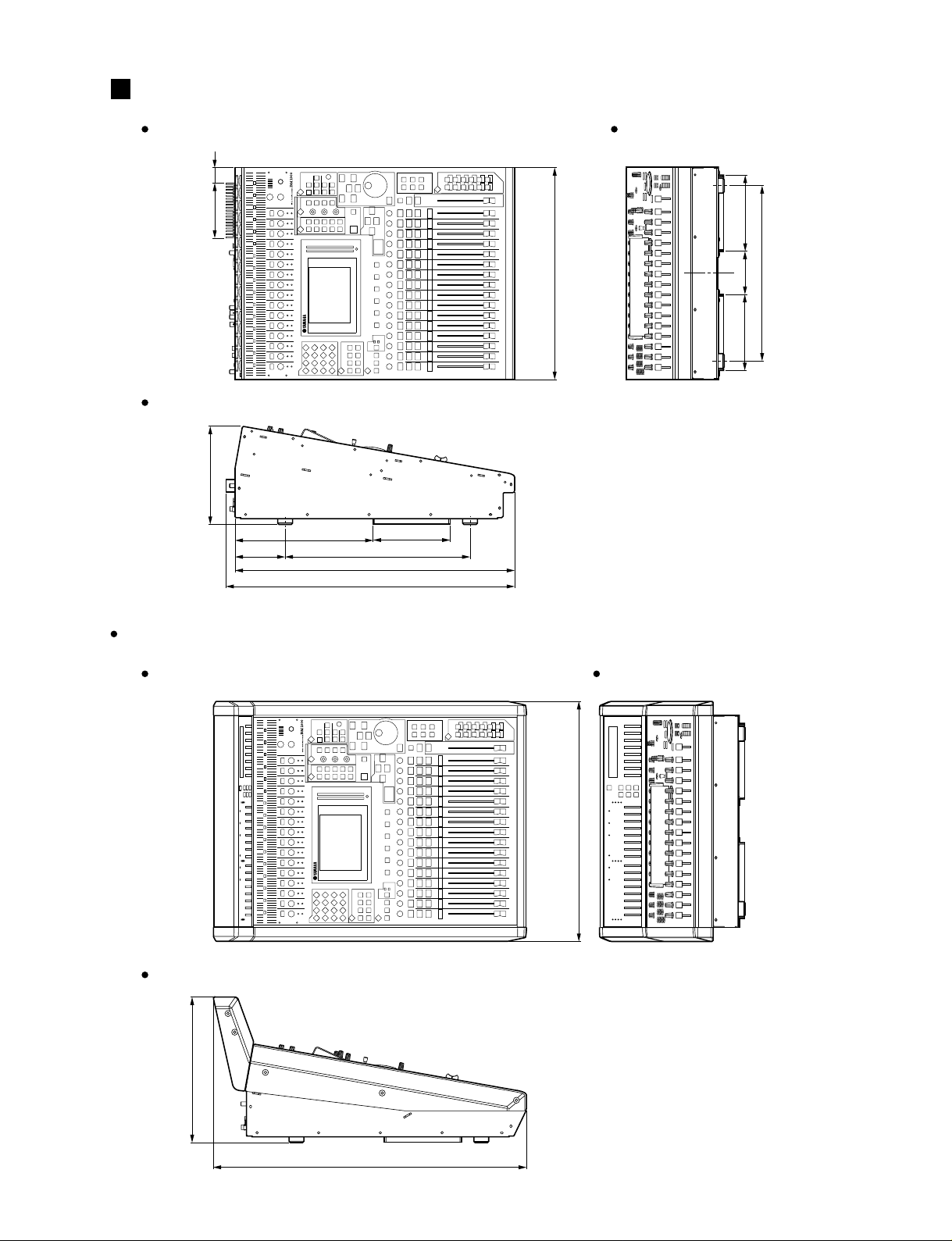
DIMENSIONS
Top view
32
112
Side view
200
(寸法図)
280
374101
565
585
156
Front view
436(Included Screw heads)
430(Not included Screw heads)
Units: mm
(単位)
154
87
154
355
With MB1000 and SP1000 installed
Top view
Side view
295
(MB1000/SP1000 取り付け時)
Front view
486
635
Units: mm
(単位)
13
Page 14
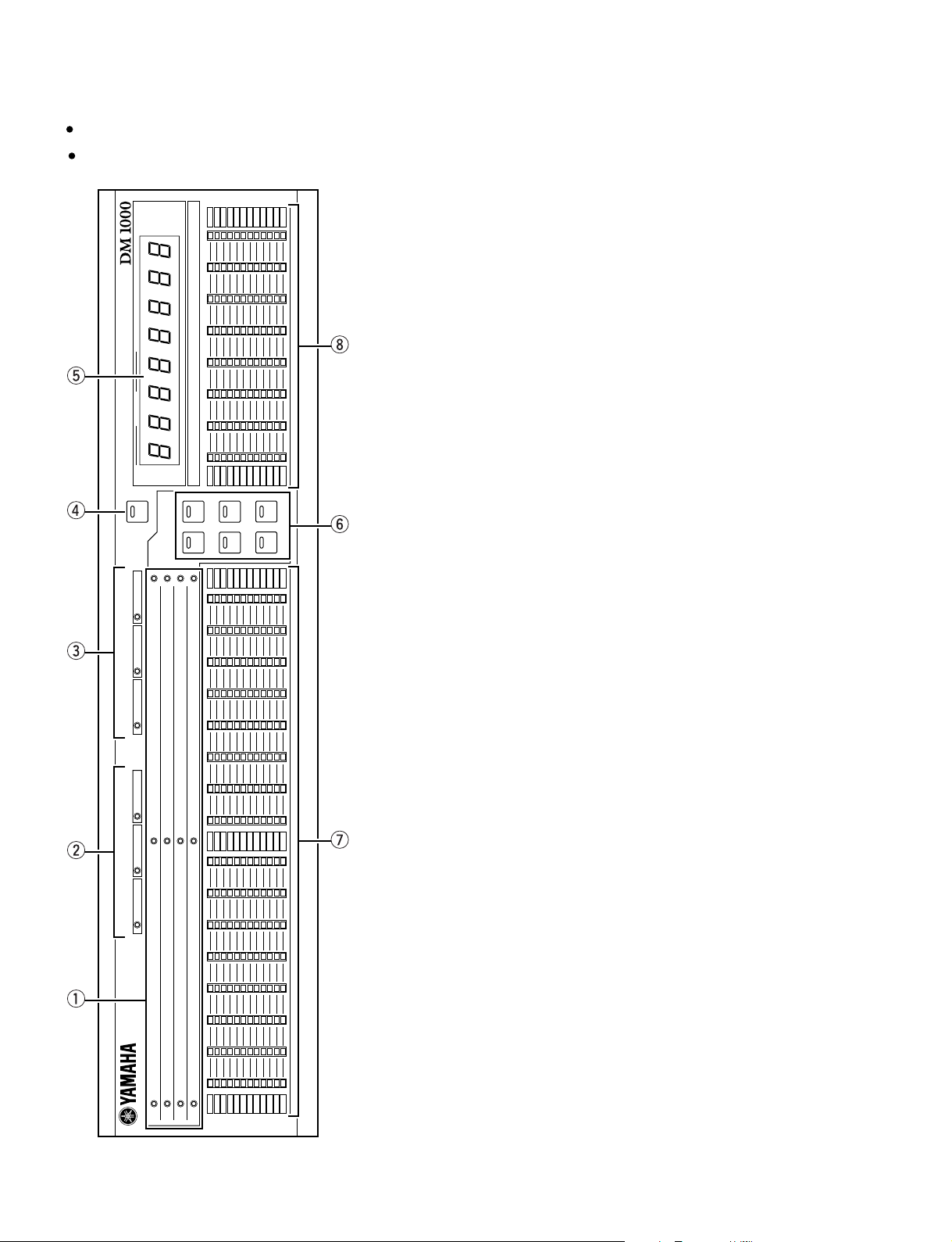
DM1000/MB1000/SP1000
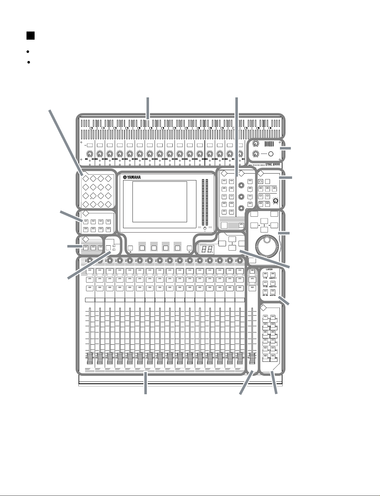
PANEL LAYOUT
DM1000
Control Panel
DISPLAY ACCESS Section (p. 17)
(ディ スプレイアクセスセクシ ョン)
AUX SELECT
Section (p. 16)
(AUX選択
セクシ ョ ン)
ENCODER
MODE Section
(p. 16)
(エンコーダー
モー ドセ クショ ン)
FADER MODE
Section (p. 16)
フ ェ ーダーモード
(
セクシ ョ ン
)
(コントロールパネル)
1
+48V
ONOFF
1
PAD
20dB
20dB 20dB 20dB 20dB 20dB 20dB 20dB 20dB 20dB 20dB 20dB 20dB 20dB 20dB 20dB
-60
-16
-16
GAIN
GAIN
PEAK
PEAK
SIGNAL
SIGNAL
DISPLAY ACCESS
AUTOMIX DIO SETUP UTILITY
MIDI REMOTE METER VIEW
/
PAIR/GROUP
INSERT/DELAY
PAN/
EFFECTSURROUND DYNAMICS SCENE
AUX SELECT
DISPLAY
AUX2 AUX3 AUX4
AUX6AUX 5 AUX7 AUX8
ENCODER MODE
DISPLAY
AUXPAN
ASSIGN
SEL
SEL
SOLO
SOLO
ON
ON
1
2
+10
+10
0
5
5
5
0
0
10
5
5
15
20
10
10
15
15
30
20
20
40
50
30
30
60
40
40
70
50
50
(パネルレイアウト)
AD Input Section (p. 15)
(ADイン プットセクション)
5
2
+48V
-60
INPUT
PATCH
0
5
10
15
20
30
40
50
60
70
ONOFF
-16
GAIN
PEAK
SIGNAL
OUTPUT
PATCH
FADER MODE
SEL
SOLO
ON
3
+10
5
0
5
10
15
20
30
40
50
4
3
+48V
+48V
ONOFF
ONOFF
-60
-60
-16
-16
GAIN
GAIN
PEAK
PEAK
SIGNAL
SIGNAL
FADER
AUX
SEL
SEL
SOLO
SOLO
ON
ON
4
5
+10
+10
0
0
5
5
5
5
0
0
10
10
5
5
15
15
20
20
10
10
15
15
30
30
20
20
40
40
50
50
30
30
60
60
40
40
70
70
50
50
6
78 12131415
+48V
+48V
ONOFF
-60
-16
GAIN
PEAK
SIGNAL
+48V
ONOFF
-60
-60
-16
GAIN
PEAK
SIGNAL
+48V
ONOFF
ONOFF
-60
-60
-16
-16
-16
GAIN
GAIN
PEAK
SIGNAL
GAIN
PEAK
PEAK
SIGNAL
SIGNAL
Display Section
(p. 17)
(ディ スプレイセクショ ン)
F1 F2 F3
SEL
SOLO
ON
6
+10
+10
0
0
5
5
5
5
0
0
10
10
5
5
15
15
20
20
10
10
15
15
30
30
20
20
40
40
50
50
30
30
60
60
40
40
70
70
50
50
SEL
SOLO
SOLO
ON
7
+10
0
5
5
0
10
5
15
20
10
15
30
20
40
50
30
60
40
70
50
F4
SEL
ON
8
SEL
SEL
SOLO
SOLO
ON
ON
9
+10
+10
0
0
5
5
5
5
0
0
10
10
5
5
15
15
20
20
10
10
15
15
30
30
20
20
40
40
50
50
30
30
60
60
40
40
70
70
50
50
91011
+48V
+48V
ONOFF
-60
-16
GAIN
PEAK
SIGNAL
OVER
0
-2
-4
-6
-8
-10
-12
-14
-18
-24
-30
-36
-42
-48
-56
-72
LR
SEL
SOLO
ON
+10
0
5
5
0
10
5
15
20
10
15
30
20
40
50
30
60
40
70
50
+48V
-60
-16
GAIN
PEAK
SIGNAL
OVER
-2
-4
-6
-8
-10
-12
-14
-18
-24
-30
-36
-42
-48
-56
-72
SEL
SOLO
ON
+10
0
5
5
0
10
5
15
20
10
15
30
20
40
50
30
60
40
70
50
ONOFF
-60
-16
GAIN
PEAK
SIGNAL
SEL
SOLO
ON
+10
0
5
5
0
10
5
15
20
10
15
30
20
40
50
30
60
40
70
50
SELECTED CHANNEL Section (p. 18)
(セ レ ク テ ッドチ ャ ン ネルセクシ ョン)
ONOFF
-60
-16
GAIN
PEAK
SIGNAL
0
SEL
SOLO
ON
+10
0
5
5
0
10
5
15
20
10
15
30
20
40
50
30
60
40
70
50
+48V
+48V
ONOFF
ONOFF
1615141312111098765432
-60
-60
-16
-16
GAIN
GAIN
PEAK
PEAK
SIGNAL
SIGNAL
SELECTED CHANNEL
ROUTING
DISPLAY
DISPLAY
12
34
56
FREQUENCY
78
GAIN
STEREO DIRECT
GRAB
SCENE MEMORY
STORE R ECALL
SEL
SEL
SOLO
SOLO
ON
ON
16151413121110
+10
+10
0
0
5
5
5
5
0
0
10
10
5
5
15
15
20
20
10
10
15
15
30
30
20
20
40
40
50
50
30
30
60
60
40
40
70
70
50
50
Q
-60
0
5
10
15
20
30
40
50
60
70
+48V
ONOFF
EQUALIZER
HIGH
HIGH MID
LOW MID
LOW
0
5
10
15
20
30
40
50
60
70
+48V
010
TALKBACK LEVEL
010
PHONES
LEVEL
DEC
ENTER
AUTO
SEL
ON
ONOFF
DISPLAY
SOLO CLE AR
2TR D1
SLOT
DIMMER
DISPLAY
16
+48V
ONOFF
PHONES
MONITOR
STEREO
2TR D2
BUS
MONITOR
TALKBACK
LEVEL
INC
USER DEFINED
KEYS
100
(シーンメモ リーセクシ ョ ン)
(レイヤーセクショ ン)
Headphones
& Talkback
Section
(p. 19)
(ヘッドフォン/
ト ークバ ックセ クション)
MONITOR
Section (p. 20)
(モニターセクショ ン)
Data Entry
Section (p. 19)
(データエン トリー
セクシ ョ ン)
SCENE MEMORY
Section (p. 18)
LAYER Section
(p. 18)
14
1
2
3
4
5
17 33
AUX 1
18 34
AUX 2
19 35
AUX 3
20 36
AUX 4
21 37
AUX 5
22 38
AUX 6
6
23 39
Channel Strip Section (p. 15)
(チャンネルモ ジュールセクシ ョン)
25 41
BUS 1
10
9
26 42
28 44
27 43
BUS 4
BUS 3
BUS 2
29 45
BUS 5
30 46
STEREO Section (p. 16)
(ステレオセクション)
32 48
31 47
BUS 7
BUS 6
STEREO
BUS 8
USER DEFINED KEYS
Section (p. 19)
(ユーザー定義キーセク ショ ン)
7
8
24 40
AUX 7
AUX 8
16
15
14
13
12
11
Page 15
DM1000/MB1000/SP1000
AD Input Section
1
+48V
(ADインプットセクション)
2
+48V
ONOFF
ONOFF
1
PAD
20dB
20dB 20dB 20dB 20dB 20dB 20dB 20dB 20dB 20dB 20dB 20dB 20dB 20dB 20dB 20dB
-60
-60
-16
-16
GAIN
GAIN
PEAK
PEAK
SIGNAL
SIGNAL
-60
-16
GAIN
PEAK
SIGNAL
Channel Strip Section
5
+48V
GAIN
PEAK
SIGNAL
6
78 1213
+48V
+48V
ONOFF
ONOFF
-60
-60
-16
-16
GAIN
GAIN
PEAK
PEAK
SIGNAL
SIGNAL
+48V
ONOFF
ONOFF
-60
-60
-16
-16
GAIN
PEAK
SIGNAL
4
3
+48V
+48V
ONOFF
ONOFF
-60
-16
GAIN
PEAK
SIGNAL
-60
-16
-16
GAIN
PEAK
SIGNAL
q [+48V ON/OFF] switches 1-16
w [PAD] switches 1-16
e [GAIN] controls 1-16
r [PEAK] indicators 1-16
t [SIGNAL] indicators 1-16
(チャンネルモジュールセクション)
91011
+48V
+48V
+48V
GAIN
PEAK
SIGNAL
ONOFF
ONOFF
-60
-60
-16
GAIN
PEAK
SIGNAL
-60
-16
-16
GAIN
PEAK
SIGNAL
GAIN
PEAK
SIGNAL
+48V
ONOFF
ONOFF
-60
-60
-16
-16
GAIN
GAIN
PEAK
PEAK
SIGNAL
SIGNAL
(+48Vオン/オフスイッチ 1〜16)
(パッドスイッチ 1〜16)
(ゲインコントロール 1〜16)
(ピークインジケーター 1〜16)
(シグナルインジケーター 1〜16)
16
15
14
+48V
+48V
+48V
ONOFF
ONOFF
+48V
ONOFF
ONOFF
1615141312111098765432
-60
-60
-16
GAIN
PEAK
SIGNAL
SOLO
+10
5
0
5
10
15
20
30
40
50
17 33
SEL
ON
1
0
5
10
15
20
30
40
50
60
70
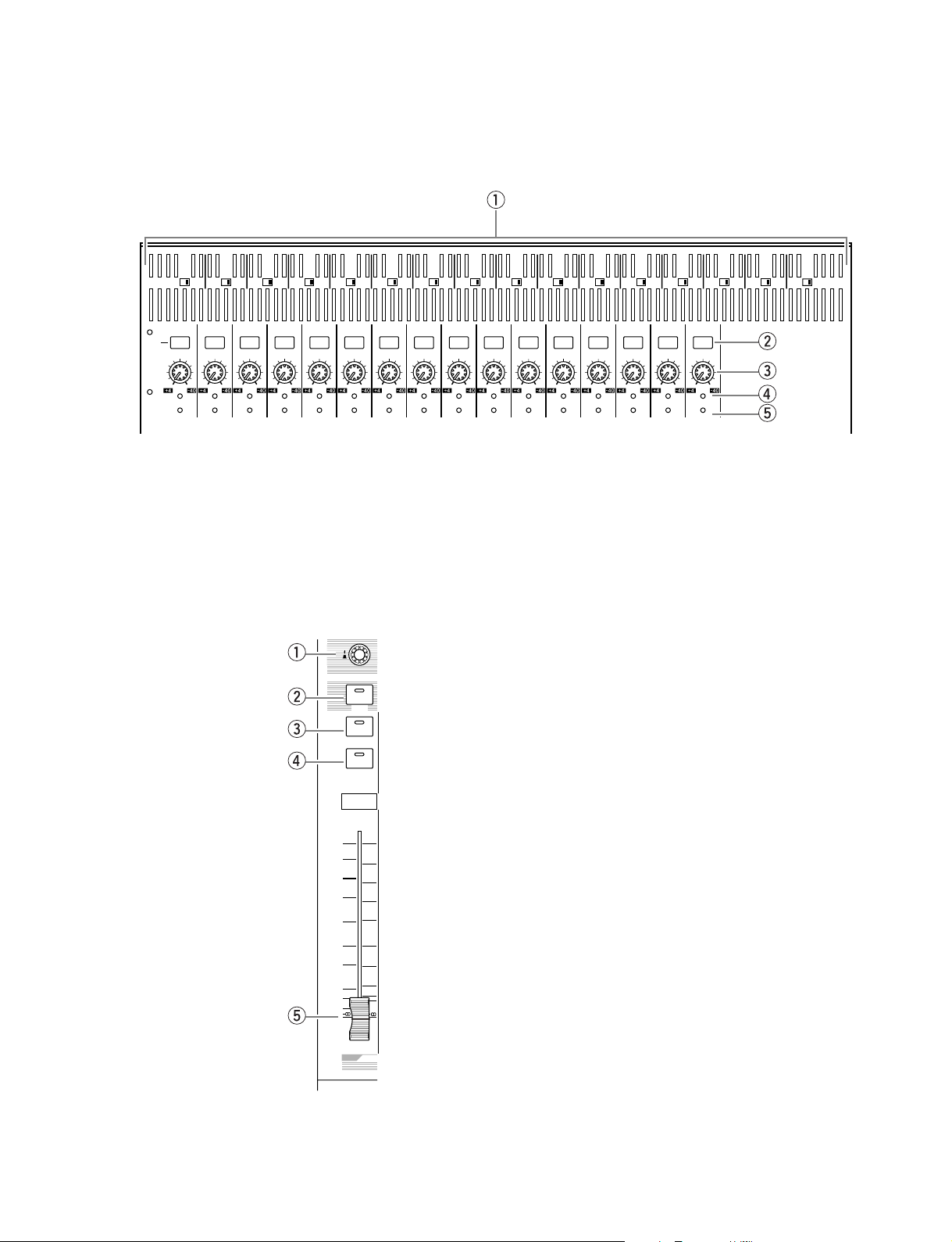
q Encoders 1-16
w [SEL] buttons 1-16
e [SOLO] buttons 1-16
r [ON] buttons 1-16
t Channel faders 1-16
(エンコーダー 1〜16)
(セレクトキー 1〜16)
(ソロキー 1〜16)
(オンキー 1〜16)
(チャンネルフェーダー 1〜16)
1
AUX
1
15
Page 16
DM1000/MB1000/SP1000
STEREO Section
(ステレオセクション)
AUTO
SEL
ON
0
5
10
15
20
30
40
50
60
70
STEREO
q [AUTO] button
w [SEL] button
e [ON] button
r [STEREO] fader
(オートキー)
(セレクトキー)
(オンキー)
(ステレオフェーダー)
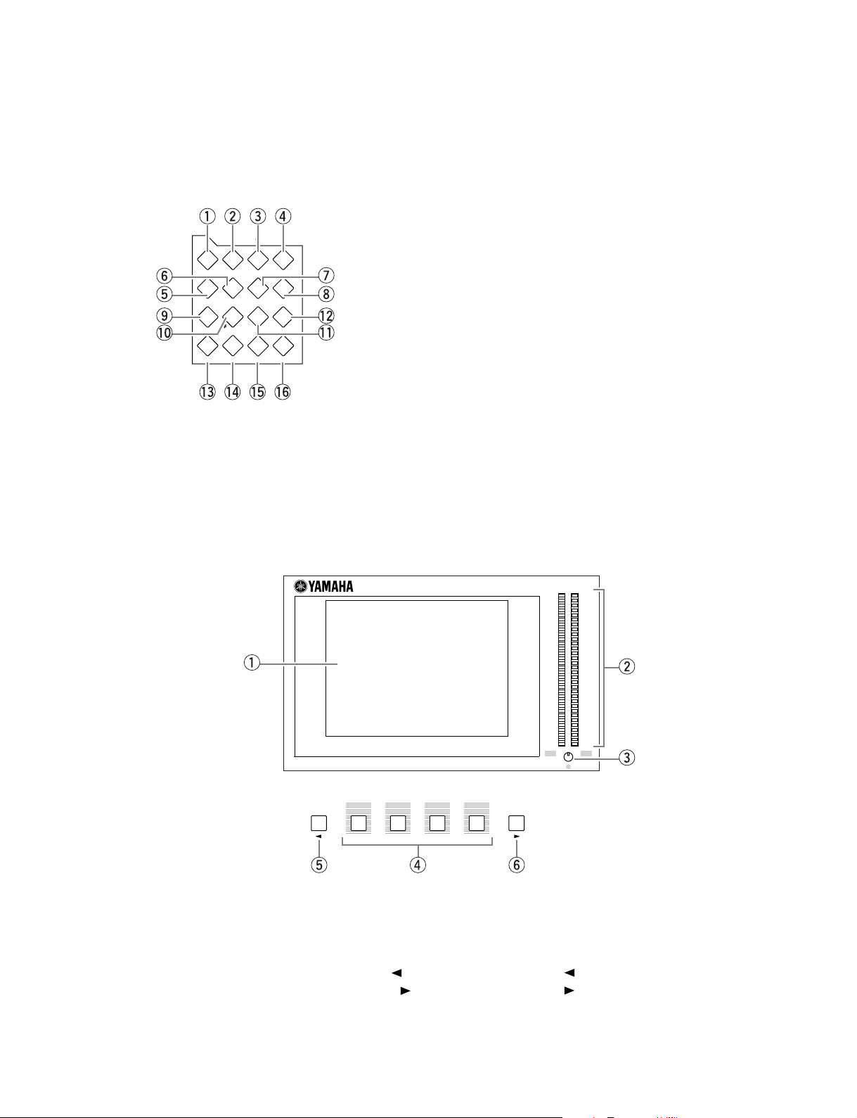
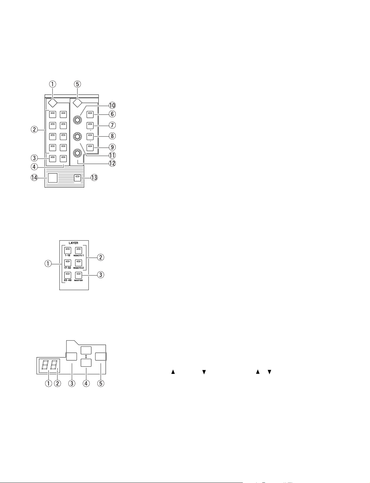
AUX SELECT Section
(AUX 選択セクション)
AUX SELECT
DISPLAY
AUX2AUX3AUX
AUX
1
AUX
6
AUX
5
ENCODER MODE Section
ENCODER MODE
DISPLAY
FADER MODE Section
(フェーダーモードセクション)
FADER MODE
q [DISPLAY] button
w [AUX 1]–[AUX 8] buttons
AUX7AUX
4
8
(エンコーダーモードセクション)
q [DISPLAY] button
AUXPAN
ASSIGN
w [PAN] button
e [AUX] button
r [ASSIGN] button
FADER
AUX
q [FADER/AUX] button
w [FADER] indicator
e [AUX] indicator
(ディスプレイキー)
([AUX1]〜[AUX8]キー)
(ディスプレイキー)
(パンキー)
([AUX]キー)
(アサインキー)
(フェーダー /AUXキー)
(フェーダーインジケーター)
([AUX]インジケーター)
16
Page 17
DM1000/MB1000/SP1000
DISPLAY ACCESS Section
DISPLAY ACCESS
AUTOMIX DIO SETUP UTILITY
MIDI REMOTE METER VIEW
INPUT
/
PAIR/GROUP
INSERT/DELAY
PATC H
PAN/
Display Section
EFFECTSURROUND DYNAMICS SCENE
(ディスプレイセクション)
(ディスプレイアクセスセクション)
q [AUTOMIX] button
w [DIO] button
e [SETUP] button
r [UTILITY] button
t [MIDI] button
y [REMOTE] button
u [METER] button
i [VIEW] button
OUTPUT
PATCH
o [PAIR/GROUP] button
!0 [
Ø
/INSERT/DELAY] button
!1 [INPUT PATCH] button
!2 [OUTPUT PATCH] button
!3 [PAN/SURROUND] button
!4 [DYNAMICS] button
!5 [EFFECT] button
!6 [SCENE] button
(オートミックスキー)
(デジタル入出力キー)
(セットアップキー)
(ユーティリティーキー)
(ミディキー)
(リモートキー)
(メーターキー)
(ビューキー)
(ペア /グループキー)
(フェーズ /インサート/ ディレイキー)
(インプットパッチキー)
(アウトプットパッチキー)
(パン /サラウンドキー)
(ダイナミクスキー)
(エフェクトキー)
(シーンキー)
F
1
q Display
w Stereo meters
e Contrast control
r [F1]-[F4] buttons
t Left Tab Scroll [
y Right Tab Scroll [
F
2
] button
] button
OVER
0
-2
-4
-6
-8
-10
-12
-14
-18
-24
-30
-36
-42
-48
-56
-72
LR
F
4
F
3
(ディスプレイ)
(ステレオメーター)
(コントラスト調整ノブ)
([F1]〜[F4]キー)
(タブスクロール[
(タブスクロール[
OVER
0
-2
-4
-6
-8
-10
-12
-14
-18
-24
-30
-36
-42
-48
-56
-72
]キー)
]キー)
17
Page 18
DM1000/MB1000/SP1000
SELECTED CHANNEL Section
SELECTED CHANNEL
ROUTING
DISPLAY
12
34
56
78
STEREO DIRECT
LAYER Section
EQUALIZER
DISPLAY
HIGH
Q
HIGH MID
LOW MID
FREQUENCY
LOW
GAIN
GRAB
(レイヤーセクション)
(セレクテッドチャンネルセクション)
q ROUTING [DISPLAY] button
w ROUTING [1]–[8] buttons
e ROUTING [STEREO] button
r ROUTING [DIRECT] button
t EQUALIZER [DISPLAY] button
y EQUALIZER [HIGH] button
u EQUALIZER [HIGH-MID] button
i EQUALIZER [LOW-MID] button
o EQUALIZER [LOW] button
!0 EQUALIZER [Q] control
!1 EQUALIZER [FREQUENCY] control
!2 EQUALIZER [GAIN] control
!3 [GRAB] button
!4 Joystick
(ルーティングディスプレイキー)
(ルーティング[1]〜[8]キー)
(ルーティングステレオキー)
(ルーティングダイレクトキー)
(イコライザーディスプレイキー)
(イコライザーハイキー)
(イコライザーハイ -ミッドキー)
(イコライザーロー -ミッドキー)
(イコライザーローキー)
(イコライザー[Q]コントロール)
(イコライザーフリーケンシー
コントロール)
(イコライザーゲインコントロール)
(グラブキー)
(ジョイスティック)
SCENE MEMORY Section
SCENE MEMORY
STORE R ECALL
q [1–16]/[17–32]/[33–48] buttons
w [REMOTE 1]/[REMOTE 2] buttons
e [MASTER] button
(シーンメモリーセクション)
q Scene memory display
w Edit indicator
e [STORE] button
r Scene Up [
t [RECALL] button
([1-16]/[17-32]/[33-48]キー)
(リモート 1/リモート2キー)
(マスターキー)
] / Down [ ] buttons
(シーンメモリーディスプレイ)
(エディットインジケーター)
(ストアキー)
(シーン[
]/[ ]キー)
(リコールキー)
18
Page 19
DM1000/MB1000/SP1000
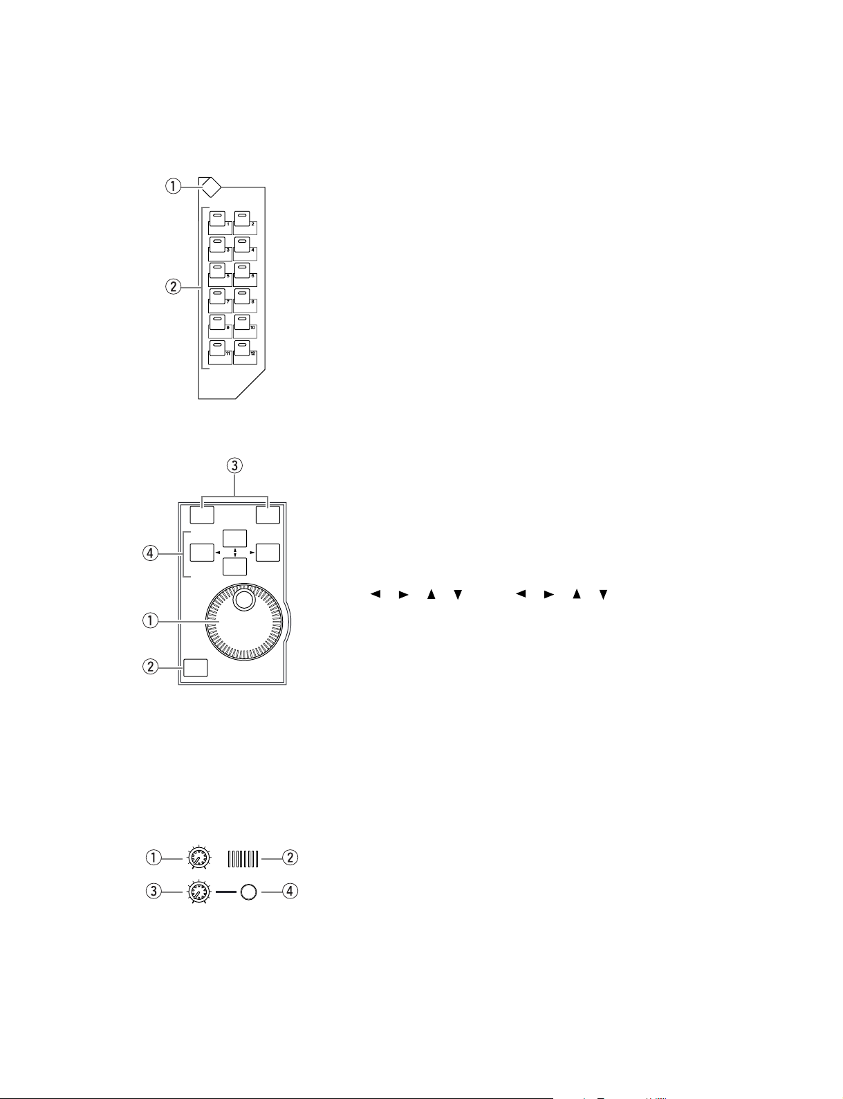
USER DEFINED KEYS Section
USER DEFINED
KEYS
DISPLAY
Data Entry Section
(データエントリーセクション)
DEC
INC
(ユーザー定義キーセクション)
q [DISPLAY] button
w [1]-[12] buttons
(ディスプレイキー)
([1]〜[12]キー)
q Parameter wheel
w [ENTER] button
e [DEC] & [INC] buttons
r Left, Right, Up, Down
([
]/[ ]/[ ]/[ ])
cursor buttons
(パラメーターホイール)
(エンターキー)
([DEC]/[INC]キー)
(カーソル左、右、上、下
([
]/[ ]/[ ]/[ ])キー)
ENTER
Headphones & Talkback Section
010
TALKBACK LEVEL
010
PHONES
LEVEL
PHONES
(ヘッドフォン/トークバックセクション)
q [TALKBACK LEVEL] control
w Talkback mic
e [PHONES LEVEL] control
r [PHONES] jack
(トークバックレベルコントロール)
(トークバックマイク)
(ヘッドフォンレベルコントロール)
(ヘッドフォン端子)
19
Page 20
DM1000/MB1000/SP1000
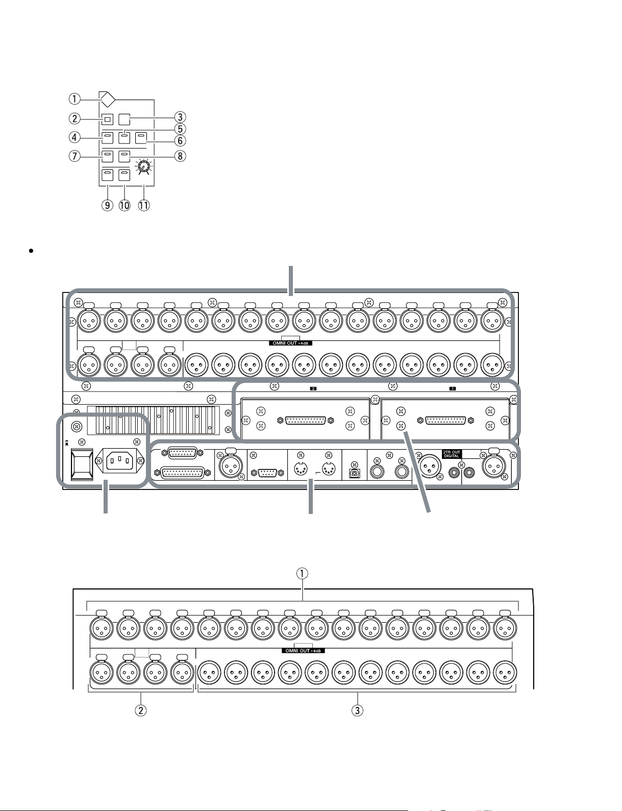
MONITOR Section
DISPLAY
SOLO CLEAR
2TR D1
SLOT
DIMMER
Rear Panel
(リアパネル)
16
4
(モニターセクション)
MONITOR
2TR D2
STEREO
BUS
100
MONITOR
TALKBACK
LEVEL
OMNI
213
IN
q [DISPLAY] button
w [SOLO] indicator
e [CLEAR] button
r [2TR D1] button
t [2TR D2] button
y [STEREO] button
u [SLOT] button
i [BUS] button
o [DIMMER] button
!0 [TALKBACK] button
!1 [MONITOR LEVEL] control
(ディスプレイキー)
(ソロインジケーター)
(クリアキー)
([2TRD1]キー)
([2TRD2]キー)
(ステレオキー)
(スロットキー)
(バスキー)
(ディマーキー)
(トークバックキー)
(モニターレベルコントロール)
AD Input and Output Section (p. 20)
(ア ナログ入出力セクション)
INPUT
23456781101112131415 9
1
2
13456781101112 9
POWER
ON
OFF
AC IN
METER
CONTROL
SMPTE IN
SLOT
REMOTE MIDI
INOUT
TO HOST
USB
WORD CLOCK
INOUT
SLOT
1
Power Section (p. 21) Digital I/O & Control Section (p. 21) SLOT Section (p. 21)
(電源セク ション)
AD Input and Output Section
16
4
OMNI
213
IN
(デジタルイン/アウト、コン トロールセ ク ション )
(アナログ入出力セクション)
INPUT
(スロ ットセクション)
2TR IN
DIGITAL
2
2
COAXIAL AES/EBUCOAXIALAES/EBU
1
23456781101112131415 9
1
2
13456781101112 9
20
q [INPUT] connectors 1-16
w [OMNI IN] connectors 1-4
e [OMNI OUT] connectors 1-12
(インプット端子 1〜16)
(オムニイン端子 1〜4)
(オムニアウト端子 1〜12)
Page 21
DM1000/MB1000/SP1000
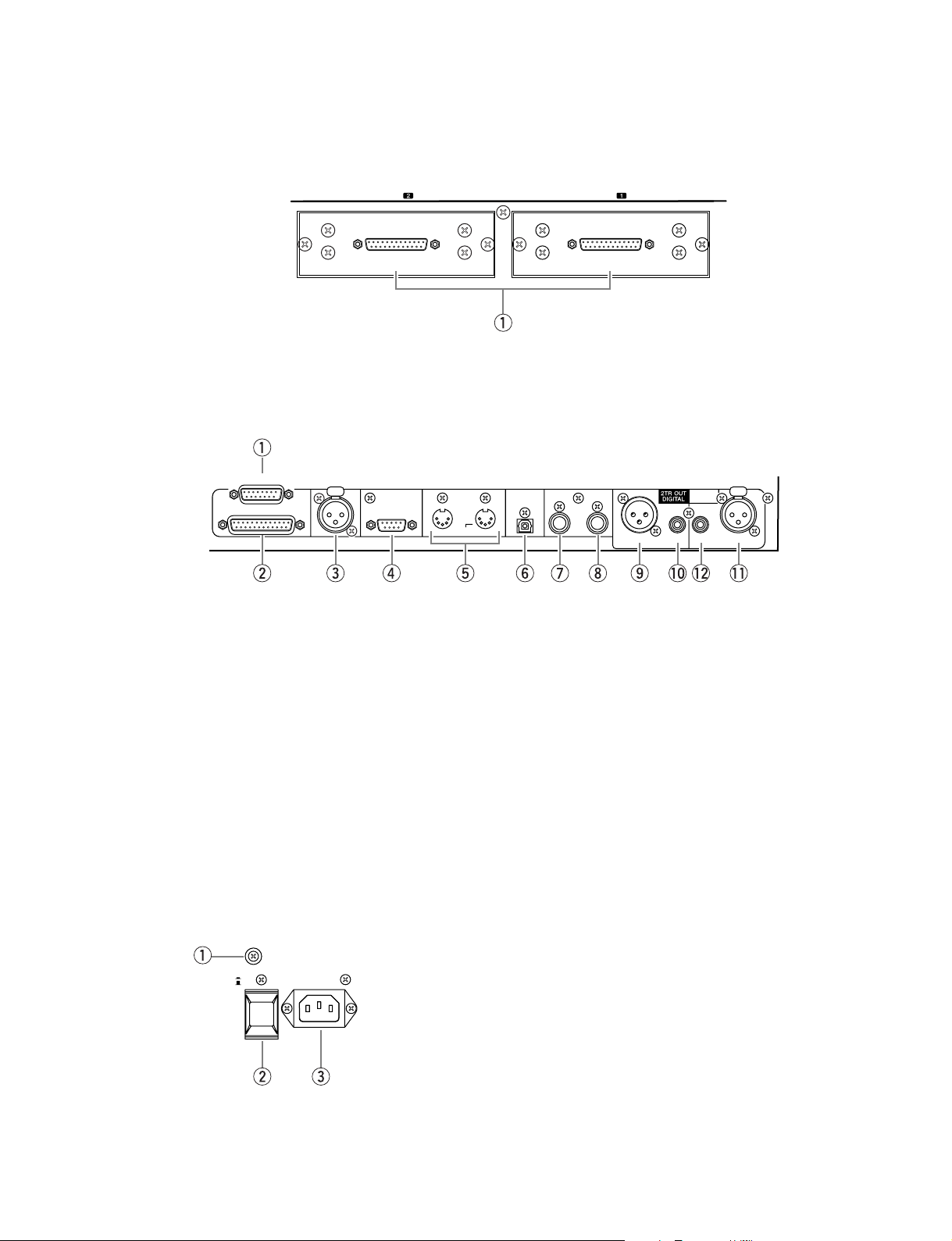
SLOT Section
(スロットセクション)
Digital I/O & Control Section
METER
CONTROL
q [METER] connector
w [CONTROL] connector
e [SMPTE TIME CODE INPUT] connector
r [REMOTE] connector
t [MIDI IN & OUT] ports
y [TO HOST USB] port
u [WORD CLOCK OUT] connector
i [WORD CLOCK IN] connector
o [2TR OUT DIGITAL AES/EBU 1] connector
!0 [2TR OUT DIGITAL COAXIAL 2] connector
!1 [2TR IN DIGITAL AES/EBU 1] connector
!2 [2TR IN DIGITAL COAXIAL 2] connector
SLOT
q [SLOT 1] & [SLOT 2]
(スロット 1/2)
SLOT
(デジタルイン /アウト、コントロールセクション)
SMPTE IN
REMOTE MIDI
INOUT
TO HOST
USB
WORD CLOCK
INOUT
(メーター端子)
(コントロール端子)
(SMPTE タイムコードインプット端子)
(リモート端子)
(ミディイン/アウトポート)
(トゥホストUSBポート)
(ワードクロックアウト端子)
(ワードクロックイン端子)
(2 トラックデジタルアウトAES/EBU1端子)
(2 トラックデジタルアウトCOAXIAL2端子)
(2 トラックデジタルインAES/EBU1端子)
(2 トラックデジタルインCOAXIAL2端子)
2TR IN
1
DIGITAL
2
2
COAXIAL AES/EBUCOAXIALAES/EBU
1
Power Section
(電源セクション)
POWER
ON
OFF
AC IN
q Grounding screw
w [POWER ON/OFF] switch
e [AC IN] connector
(アース用ネジ)
(電源オン/オフスイッチ)
([ACIN]ソケット)
21
Page 22
DM1000/MB1000/SP1000
MB1000
Controls
(コントロール類)
0
OVER
CLOCK
BEAT
PEAK METER BRIDGE MB1000 FOR
MEASURE
HM S F
0
TIME CODE
PRE EQ PRE FADER POST FADERPRE EQ PRE FADER POST FADER
PEAK HOLD
163248
153147
143046
132945
122844
OVER
1
REMOTE
1-16
0
OVER
-3-6-9
-3-6-9
-3-6-9
-12
-15
-18
-24
-30
-36
-48
q Channel indicators
(チャンネルインジケーター)
-12
-15
-18
-24
-30
-36
-48
2
MASTER
REMOTE
33-48
17-32
w [INPUT METERING POSITION] indicators
(インプットメーターポジションインジケーター)
e [OUTPUT METERING POSITION] indicators
(アウトプットメーターポジションインジケーター)
r [PEAK HOLD] button
(ピークホールドキー)
-12
-15
-18
-24
-30
-36
-48
t [TIME CODE] display
(タイムコードディスプレイ)
y [1-16] / [17-32] / [33-48] / [REMOTE 1] / [REMOTE 2] / [MASTER] buttons
([1-16]/[17-32]/[33-48]/リモート1/リモート2/マスターキー)
u Level meters
(レベルメーター)
i Bus meters
(バスメーター)
22
27
43
11
102642
9
25
41
8
INPUT METERING POSITION OUTPUT METERING POSITION
7
6
5
4
3
2
1
OVER
24
40
AUX 8AUX 7AUX 6AUX 5AUX 4AUX 3AUX 2AUX 1 BUS 8BUS 7BUS 6BUS 5BUS 4BUS 3BUS 2BUS 1 BUS 8BUS 7BUS 6BUS 5BUS 4BUS 3BUS 2BUS 1
23
39
22
38
21
37
20
36
19
35
18
34
17
33
OVER
0
0
-3-6-9
-3-6-9
-12
-15
-18
-24
-30
-36
-48
-12
-15
-18
-24
-30
-36
-48
Page 23
DM1000/MB1000/SP1000
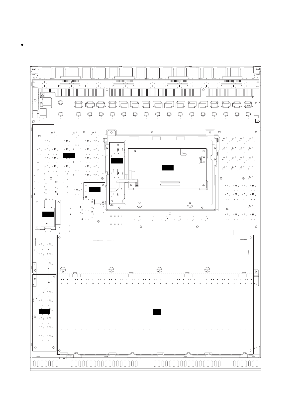
CIRCUIT BOARD LAYOUT
DM1000
Bottom Assembly
<Top view>
OPT
(ボトム Ass'y)
(ユニットレイアウト)
DCA
4/5
DCA
DCA
2/5
1/5
DCA
3/5
<Rear view>
DCA
4/5
DCA
3/5
MAIN
Power transformer
(電源トランス)
DCD
OPT
DCA
AC
2/5
JK2
JK1
23
Page 24
DM1000/MB1000/SP1000
<Top view>
JK1
JK2
DCA
AC
1/5
<Rear view>
MAIN
Power transformer
(電源トランス)
DCD
24
AC
JK2
JK1
Page 25
Rear Assembly U
<Top view>
XLR
DM1000/MB1000/SP1000
(リア上 Ass'y)
HAAD 2/2
HAAD 1/2
<Rear view>
ADA
XLR
25
Page 26
DM1000/MB1000/SP1000
Control Panel Asembly
<Bottom view>
PN1 (1/4)
(コンパネ Assy)
PN1
(2/4)
LCD
PN1
(4/4)
PN2
PN1
(3/4)
FD
26
Page 27
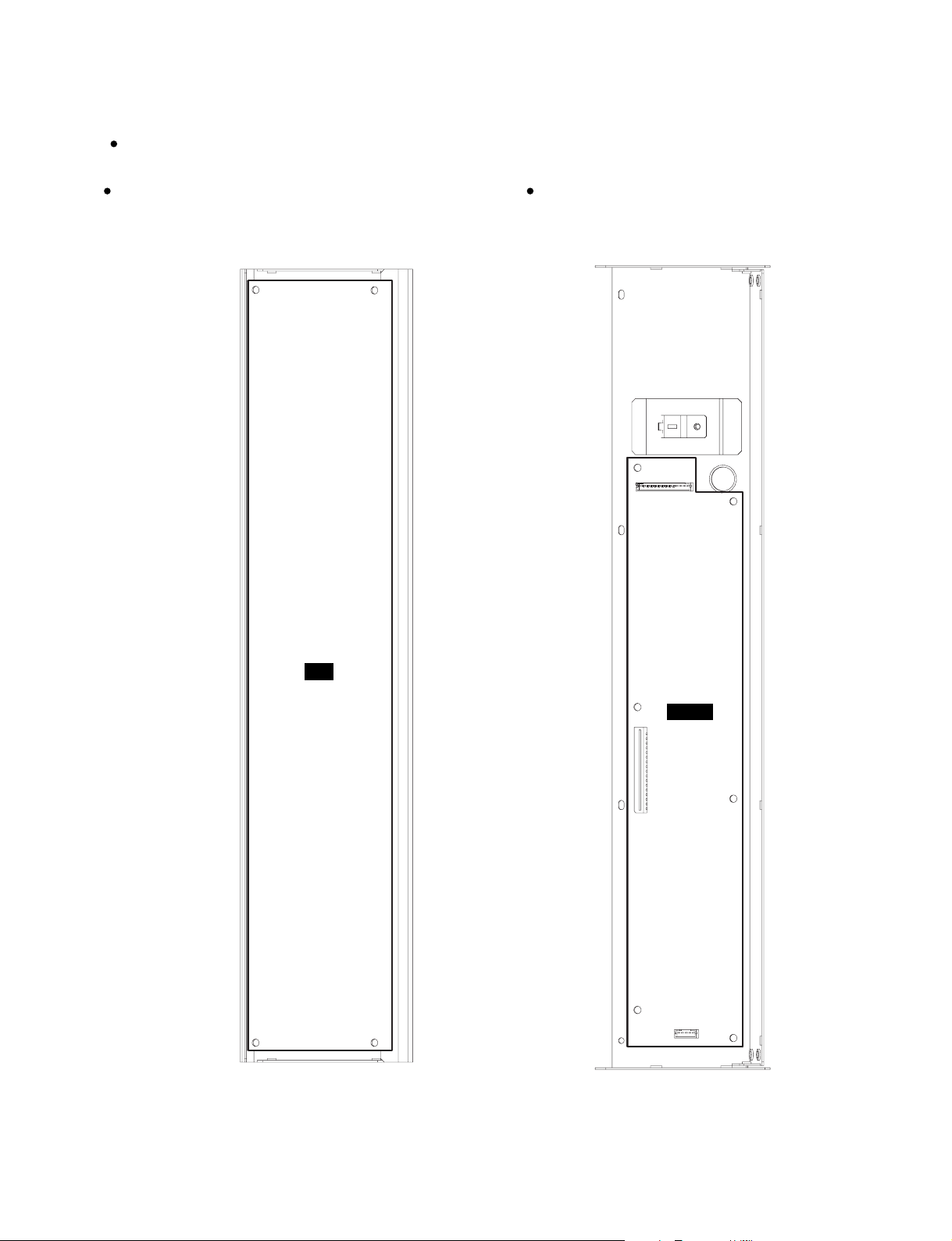
MB1000
DM1000/MB1000/SP1000
Front Panel Assembly
(フロントパネルAss'y)
Rear Panel Assembly
<Front view><Rear view>
(リアパネル Ass'y)
PN
MAIN
27
Page 28
DM1000/MB1000/SP1000
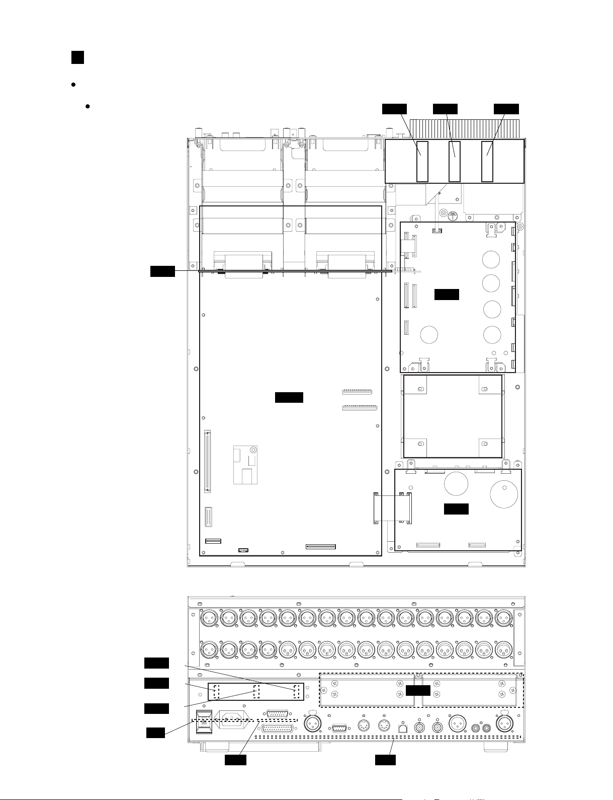
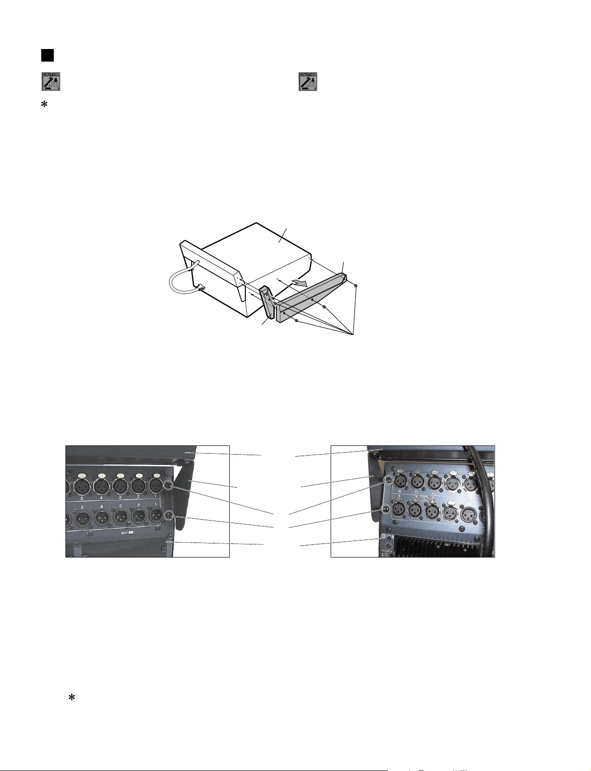
DISASSEMBLY PROCEDURE
(分解手順)
Note: Take care not to trap your fingers.
After replacing the circuit boar d or fader of FD , please
calibrate the faders. (See page 150.)
Disassembling the DM1000
1. Removing the SP1000
(Time required: About 2 minutes)
1-1. If the SP1000 is attached to the DM1000, remove
the ten (10) screws marked [A], and then both sides
must be removed. (Fig.1)
SP1000
(MB side pad)
注意:作業中は指を挟まない様に注意してください。
※FDシート又はフェーダーを交換後は、フェーダーのキャ
リブレーションを実施してください。(150ページ参照)
DM1000 の分解
1. SP1000の取り外し
1-1. DM1000にSP1000が取り付けられている場合は、
[A]のネジ10本を外して、左右共に取り外します。
(図 1)
DM1000
SP1000
(Side pad)
[A]
(所要時間:約 2分)
[A]: Bind Head Screw PW 4.0X20 MFZN2BL (VA314000)
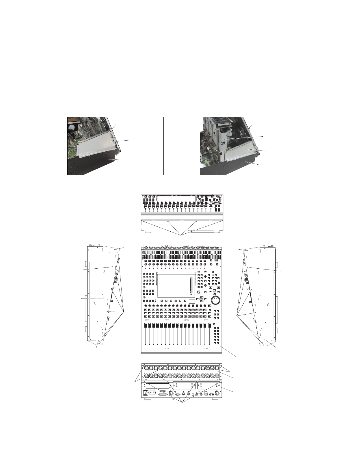
2. Removing the MB1000
(Time required: About 1 minute)
2-1. Remove the two (2) screws marked [B] and loosen
the two (2) screws marked [C]. The MB1000 can
then be removed from the DM1000. (Photo.1, 2)
[B]: Bind Head Screw A4.0X12 MFZN2BL (VP156900)
[C]: Bind Head Screw A4.0X12 MFZN2BL (VP156900)
Photo.1 Photo.2
(写真1)
3. Control Panel Assembly
(Time required: About 7 minutes)
3-1. Remove the SP1000. (See procedure 1.)
3-2. Remove the MB1000. (See procedure 2.)
3-3. Remove the twenty (20) screws marked [60A]. (Fig.2)
3-4. Lift the control panel assembly from the rear side
and fasten them by the stay. (Photo.3-1)
When assembling the control panel assembly
with the bottom assembly, put the screws of
the front side → right side panel side → left
28
side panel side → rear side in order.
(+バインド小ネジ)
(図1)
Fig.1
2. MB1000の取り外し(所要時間:約 1 分)
2-1. [B] のネジ 2 本を外し、[ C ] のネジ 2 本を緩め、
MB1000
Meter angle L, R
(メーターアングルL,R)
[B]
[C]
DM1000
(+バインド小ネジ)
(+バインド小ネジ)
3. コンパネAss'y(所要時間:約 7 分)
3-1. SP1000 を取り外します。(1項参照)
3-2. MB1000 を取り外します。(2項参照)
3-3. [60A]のネジ20本を外します。(図2)
3-4. コンパネAss'y をリア側から持ち上げ、ステイ1個
DM1000から MB1000を取り外します。(写真 1,2)
(写真2)
で固定します。(写真3-1)
※コンパネAss'yとボトムAss'yを組み立てる際
は、フロント側→右サイドパネル側→左サイド
パネル側→リア側の順にネジを取り付けてくだ
さい。
Page 29
DM1000/MB1000/SP1000
)
4. Rear Assembly U
(Time required: About 9 minutes)
4-1. Remove the SP1000. (See procedure 1.)
4-2. Remove the MB1000. (See procedure 2.)
4-3. Fasten the control panel assembly . (See procedure 3.)
4-4. Remove the six (6) screws marked [40A] and the
two (2) screws marked [70A]. Fasten the rear
assembly U by the stay. (Fig.2, Photo.3-2)
4-5. Remove the two (2) screws mark ed [40B]. The rear
assembly U can then be removed. (Fig.2)
Control panel assembly
(コンパネAss'y)
Stay
(ステイ)
(WA963600)
Bottom assembly
(ボトムAss'y)
Photo.3-1
(写真3-1)
<Front view>
4. リア上Ass'y(所要時間:約 9 分)
4-1. SP1000 を取り外します。(1項参照)
4-2. MB1000 を取り外します。(2項参照)
4-3. コンパネAss'yを固定します。(3項参照)
4-4. [40A]のネジ6本と[70A]のネジ2本を外して、リア上
Ass'y をステイ1個で固定します。(図 2、写真 3-2)
4-5. [40B]のネジ2本を外して、リア上Ass'yを外します。
(図 2)
Control panel assembly
(コンパネAss'y)
Rear assembly U
(リア上Ass'y)
Stay
(ステイ)
(WA963600)
Bottom assembly
(ボトムAss'y)
Photo.3-2 (写真3-2)
<Left side view>
[70A]
[40B]
<Top view>
[40A]
[60A]
Side panel L
(サイドパネルL)
[60A]
[40]: Bind Head Tapping Screw-B 4.0X8 MFZN2BL (EG340190)
[60A]: Bind Head Tapping Screw-B 4.0X8 MFZN2BL (EG340190)
[70A]: Bind Head Tapping Screw-B 3.0X6 MFZN2BL (EP600230)
<Rear view>
[60A]
[60A]
[40A]
(+バインドBタイト)
(+バインドBタイト)
(+バインドBタイト)
<Right side view>
[40A]
Control panel assembly
(コンパネAss'y)
[60A]
Rear assembly U
(リア上Ass'y)
Bottom assembly
(ボトムAss'y)
[70A]
[40B]
Side panel R
(サイドパネルR
Fig.2
(図2)
29
Page 30

DM1000/MB1000/SP1000
Bottom Assembly Section
5. DCD Circuit Board
(Time required: About 8 minutes)
5-1. Remove the SP1000. (See procedure 1.)
5-2. Remove the MB1000. (See procedure 2.)
5-3. Fasten the control panel assembly. (See procedure 3.)
5-4. Remove the four (4) screws marked [410] and the
two (2) screws marked [411]. The DCD circuit board
can then be removed. (Fig.3, Photo.4)
When removing the circuit board, if it is hard
to handle while the control panel assembly is
fixed slantwise at the stay, open it widely at
180° for the work.
6. DCA 1/5 Circuit Board
(Time required: About 12 minutes)
6-1. Remove the SP1000. (See procedure 1.)
6-2. Remove the MB1000. (See procedure 2.)
6-3. Fasten the control panel assembly. (See procedure 3.)
6-4. Remove the rear assembly U. (See procedure 4-5.)
6-5. Remove the five (5) screws marked [340] and the
four (4) screws marked [341]. The DCA 1/5 circuit
board can then be removed. (Fig.3, Photo.5)
ボトム Ass'y 部
5. DCDシート
5-1. SP1000 を取り外します。(1項参照)
5-2. MB1000 を取り外します。(2項参照)
5-3. コンパネ Ass'yを固定します。(3項参照)
5-4. [410]のネジ4 本と[411]のネジ2本を外して、DCD
シートを外します。(図3、写真4)
※シートを取り外す時に、ステイでコンパネAss'y
を45度程度に固定した状態で作業がしにくい場
合は、180 度開いて作業をしてください。
(所要時間:約 8 分)
6. DCA1/5シート(所要時間:約 12 分)
6-1. SP1000 を取り外します。(1項参照)
6-2. MB1000 を取り外します。(2項参照)
6-3. コンパネ Ass'yを固定します。(3項参照)
6-4. リア上 Ass'yを取り外します。(4-5項参照)
6-5. [340]のネジ5本と[341]のネジ 4本を外して、DCA
1/5シートを外します。(図3、写真 5)
7. DCA 2/5, 3/5 and 4/5 Circuit Boards
(Time required: About 10 minutes each)
7-1. Remove the SP1000. (See procedure 1.)
7-2. Remove the MB1000. (See procedure 2.)
7-3. Fasten the control panel assembly. (See procedure 3.)
7-4. Fasten the rear assembly U. (See procedure 4-4.)
7-5. Remove the screw marked [335]. The DCA 2/5 circuit
board can then be removed. (Fig.3, Photo.6)
The DCA 3/5 and 4/5 circuit boards can be
removed in the same manner.
8. OPT Circuit Board
(Time required: About 11 minutes)
8-1. Remove the SP1000. (See procedure 1.)
8-2. Remove the MB1000. (See procedure 2.)
8-3. Fasten the control panel assembly. (See procedure 3.)
8-4. Fasten the rear assembly U. (See procedure 4-4.)
8-5. Remove the four (4) screws marked [110A]. The IF
plate can then be removed. (Fig.3)
8-6. Remove the three (3) screws marked [12A] and the
two (2) screws marked [12B]. The bottom stay, the
OPT angle and the OPT circuit board can then be
removed. (Fig.3)
8-7. Remove the four (4) screws marked [230]. The OPT
circuit board can then be removed from the OPT
angle. (Photo.7)
7. DCA2/5、3/5、4/5シート
(所要時間:各約 10分)
7-1. SP1000 を取り外します。(1項参照)
7-2. MB1000 を取り外します。(2項参照)
7-3. コンパネ Ass'yを固定します。(3項参照)
7-4. リア上 Ass'yを固定します。(4-4項参照)
7-5. [335]のネジ1本を外して、DCA2/5シートを外し
ます。(図3、写真6)
※ DCA3/5、4/5シートも同様に外せます。
8. OPTシート(所要時間:約 11 分)
8-1. SP1000 を取り外します。(1項参照)
8-2. MB1000 を取り外します。(2項参照)
8-3. コンパネ Ass'yを固定します。(3項参照)
8-4. リア上 Ass'yを固定します。(4-4項参照)
8-5. [110A]のネジ4 本を外して、IF プレートを外しま
す。(図3)
8-6. [12A]のネジ3本と[12B]のネジ2本を外して、ボトム
ステイとOPT 金具、OPTシートを外します。(図 3)
8-7. [230]のネジ4本を外して、OPT金具からOPTシー
トを外します。(写真7)
30
Page 31

DM1000/MB1000/SP1000
9. MAIN Circuit Board
(Time required: About 12 minutes)
9-1. Remove the SP1000. (See procedure 1.)
9-2. Remove the MB1000. (See procedure 2.)
9-3. Fasten the control panel assembly . (See procedure 3.)
9-4. Remove the rear assembly U. (See procedure 4-5.)
9-5. Remove the OPT circuit board. (See procedure 8.)
9-6. Remove the ten (10) screws marked [12C]. The
MAIN circuit board can then be removed. (Fig.4)
10. Replacing the Lithium Battery
(Time required: About 7 minutes)
10-1. Remove the SP1000. (See procedure 1.)
10-2. Remove the MB1000. (See procedure 2.)
10-3. Fasten the control panel assembly. (See procedure 3.)
10-4. You can replace the lithium battery from the MAIN
circuit board. (Fig.4)
The lithium battery is not part of the MAIN
circuit board. When you replace the MAIN
circuit board, you should remove the lithium
battery from the board, and install in the holder
on the new circuit board.
Important data should be backed up by MIDI
dump. (See page 146.)
9. MAINシート(所要時間:約 12 分)
9-1. SP1000 を取り外します。(1項参照)
9-2. MB1000 を取り外します。(2項参照)
9-3. コンパネAss'yを固定します。(3項参照)
9-4. リア上Ass'yを取り外します。(4-5項参照)
9-5. OPTシートを外します。(8項参照)
9-6. [12C]のネジ10本を外して、MAINシートを外しま
す。(図4)
10. リチウム電池の交換(所要時間:約 7 分)
10-1. SP1000 を取り外します。(1 項参照)
10-2. MB1000 を取り外します。(2 項参照)
10-3. コンパネ Ass'y を固定します。(3 項参照)
10-4. MAINシート上より、リチウム電池を交換すること
が出来ます。(図4)
※リチウム電池は、MAIN シートの構成部品ではあ
りません。MAINシートを交換する際には、本体
のシートからリチウム電池を取り外して、新し
いシートに取り付けてください。
※重要なデータはあらかじめ MIDIダンプでバック
アップしてください。(148ページ参照)
11. JK2 Circuit Board
(Time required: About 12 minutes)
11-1. Remove the SP1000. (See procedure 1.)
11-2. Remove the MB1000. (See procedure 2.)
11-3. Fasten the control panel assembly. (See procedure 3.)
11-4. Fasten the rear assembly U. (See procedure 4-4.)
11-5. Remove the OPT circuit board. (See procedure 8.)
11-6. Remove the two (2) hexagonal locking screws
marked [D]. The JK2 circuit board can then be
removed. (Fig.4)
12. JK1 Circuit Board
(Time required: About 14 minutes)
12-1. Remove the SP1000. (See procedure 1.)
12-2. Remove the MB1000. (See procedure 2.)
12-3. Fasten the control panel assembly. (See procedure 3.)
12-4. Fasten the rear assembly U. (See procedure 4-4.)
12-5. Remove the OPT circuit board. (See procedure 8.)
12-6. Remove the JK2 circuit board. (See procedure 11.)
12-7. Remove the three (3) screws marked [350A]. The
heat sink and the DCAIC angle can then be removed.
(Fig.3)
12-8. Remove the three (3) screws marked [130A], the
five (5) screws marked [140], the four (4) screws
marked [145], the three (3) screws marked [150],
the two (2) hexagonal locking screws marked [160]
and the two (2) hexagonal locking screws marked
[E]. The JK1 circuit board can then be removed.
(Fig.4)
11. JK2 シート(所要時間:約 12 分)
11-1. SP1000 を取り外します。(1 項参照)
11-2. MB1000 を取り外します。(2 項参照)
11-3. コンパネ Ass'y を固定します。(3 項参照)
11-4. リア上 Ass'y を固定します。(4-4 項参照)
11-5. OPT シートを外します。(8 項参照)
11-6. [D]の六角ロックネジ 2 本を外して、JK2 シートを
外します。(図4)
12. JK1 シート(所要時間:約 14 分)
12-1. SP1000 を取り外します。(1 項参照)
12-2. MB1000 を取り外します。(2 項参照)
12-3. コンパネ Ass'y を固定します。(3 項参照)
12-4. リア上 Ass'y を固定します。(4-4 項参照)
12-5. OPT シートを外します。(8 項参照)
12-6. JK2 シートを外します。(11 項参照)
12-7. [350A] のネジ 3 本を外して、ヒートシンクと DCAIC
アングルを外します。(図3)
12-8. [130A] のネジ 3本と[140]のネジ 5本、[145]のネジ4
本、[150]のネジ3 本、[160]の六角ロックネジ2本、
[E]の六角ロックネジ2本を外して、JK1シートを外
します。(図4)
31
Page 32

DM1000/MB1000/SP1000
<Front view>
OPT angle
(OPT金具)
Bottom stay
(ボトムステイ)
Bottom stay
(ボトムステイ)
[12B]
OPT angle
(OPT金具)
[12B]
[230]
Photo.7 (写真7)
<Top view>
OPT
OPT
<Front view>
DCA 3/5
DCA 4/5
[335]
DCA 4/5
DCA 2/5
Photo.6 (写真6)
DCA 1/5
<Right side view>
[341]
DCA 1/51/51/5
Photo.5 (写真5)
Heat sink
(ヒートシンク)
DCAIC angle
(DCAICアングル)
DCA 3/5
DCA 2/5
[340]
<Front view>
[411]
DCD
DCD
IF plate
<Rear view>
[110A]
[350A]
[12]: Bind Head Tapping Screw-B 3.0X6 MFZN2BL (EP600230)
[110A]:Bind Head Screw A4.0X12 MFZN2BL (VP156900)
[230]: Bind Head Screw 4.0X8 MFZN2BL (EG340360)
[335]: Bind Head Screw SP 3.0X12 MFZN2Y (VB763800)
[340]: Bind Head Tapping Screw-B 3.0X6 MFZN2BL (EP600230)
[341]: Bind Head Tapping Screw-B SP 3.0X10 MFZN2BL (VH741100)
[350A]:Bind Head Tapping Screw-B 3.0X6 MFZN2BL (EP600230)
[410]: Bind Head Tapping Screw-B 3.0X6 MFZN2BL (EP600230)
[411]: Bind Head Tapping Screw-B SP 3.0X10 MFZN2BL (VH741100)
[12A]
(+バインドBタイト)
(+バインド小ネジ)
(+バインド小ネジ)
(+バインド小ネジ)
(+バインドBタイト)
(+バインドBタイト)
(+バインドBタイト)
(+バインドBタイト)
(+バインドBタイト)
(IFプレート)
[110A]
[12A] [12A]
[410]
OPT
Photo.4 (写真4)
32
Fig.3 (図3)
Page 33

DM1000/MB1000/SP1000
[145]
[140]
[150]
[140]
[145]
<Rear view>
<Top view>
[D]
[E]
MAIN
JK2
JK1
[12C]
[130A]
[12C]
[160]
Battery VN103500
VN103600(Battery holder for VN103500)
Notice for back-up battery removal
Push the battery as shown in figure,
then the battery will pop up.
Druk de batterij naar beneden zoals
aangeven in de tekening de batterij
springt dan naar voren.
Battery
Battery holder
Lithium Battery(リチウム電池)
JK2
JK1
AC shield plate
[60B]
[285]
[285]
[280]
Power transformer
(電源トランス)
(ACシールド金具)
[12C]: Bind Head Tapping Screw-B 3.0X6 MFZN2BL (EP600230)
[60B]: Bind Head Tapping Screw-B 4.0X8 MFZN2BL (EG340190)
[130A]:Bind Head Tapping Screw-B 3.0X6 MFZN2BL (EP600230)
[140]: Bonding Tapping Screw-B 3.0X8 MFZN2BL (VN413300)
[145]: Bind Head Tapping Screw-B 2.6X8 MFZN2BL (VB096700)
[150]: Bonding Screw 3.0X8 MFZN2BL (VP157800)
[160]: Hex. Locking Screw JFS-2.6S-BIW (VS604900)
(+ボンディング小ネジ)
(六角ロックネジ)
[280]: Bind Head Tapping Screw-B 3.0X8 MFZN2BL (EP600190)
[285]: Bind Head Tapping Screw-B 3.0X6 MFZN2BL (EP600230)
(+バインドBタイト)
(+バインドBタイト)
(+バインドBタイト)
(ボンディングBタイト)
(+バインドBタイト)
(+バインドBタイト)
(+バインドBタイト)
Fig.4 (図4)
33
Page 34

DM1000/MB1000/SP1000
13. AC Shield Plate
(Time required: About 10 minutes)
13-1. Remove the SP1000. (See procedure 1.)
13-2. Remove the MB1000. (See procedure 2.)
13-3. Fasten the control panel assembly. (See procedure 3.)
13-4. Fasten the rear assembly U. (See procedure 4-4.)
13-5. Remove the heat sink and the DCAIC angle. (See
procedure 12-7.)
13-6. Remove the four (4) screws marked [285]. The AC
shield plate can then be removed. (Fig.4)
14. Power T ransformer
(Time required: About 11 minutes)
14-1. Remove the SP1000. (See procedure 1.)
14-2. Remove the MB1000. (See procedure 2.)
14-3. Fasten the control panel assembly. (See procedure 3.)
14-4. Remove the rear assembly U. (See procedure 4-5.)
14-5. Remove the AC shield plate. (See procedure 13.)
14-6. Remove the four (4) screws marked [60B]. The power
transformer can then be removed. (Fig.4)
15. AC Circuit Board
(Time required: About 11 minutes)
15-1. Remove the SP1000. (See procedure 1.)
15-2. Remove the MB1000. (See procedure 2.)
15-3. Fasten the control panel assembly. (See procedure 3.)
15-4. Fasten the rear assembly U. (See procedure 4-4.)
15-5. Remove the AC shield plate. (See procedure 13.)
15-6. Remove the cord holder marked [265] fastened the
AC circuit board and the ferrite core.(Photo.8)
15-7. Remove the two (2) screws marked [255] and the
screw marked [290A]. The A C circuit board can then
be removed from the two (2) locking card spacers.
(Photo.8)
The power switch knob is not part of the AC
circuit board. When you replace the AC circuit
board, you should remove the power switch
knob from the AC circuit board, and install in
the new AC circuit board. (Photo.9)
13. AC シールド金具(所要時間:約 10 分)
13-1. SP1000を取り外します。(1項参照)
13-2. MB1000を取り外します。(2項参照)
13-3. コンパネAss'yを固定します。(3項参照)
13-4. リア上Ass'yを固定します。(4-4項参照)
13-5. ヒートシンクとDCAICアングルを外します。(12-7
項参照)
13-6. [285]のネジ4本を外して、ACシールド金具を外し
ます。(図4)
14. 電源トランス(所要時間:約 11 分)
14-1. SP1000を取り外します。(1項参照)
14-2. MB1000を取り外します。(2項参照)
14-3. コンパネAss'yを固定します。(3項参照)
14-4. リア上Ass'yを取り外します。(4-5項参照)
14-5. ACシールド金具を取り外します。(13項参照)
14-6. [60B]のネジ4本を外して、電源トランスを外しま
す。(図4)
15. AC シート(所要時間:約 11 分)
15-1. SP1000を取り外します。(1項参照)
15-2. MB1000を取り外します。(2項参照)
15-3. コンパネAss'yを固定します。(3項参照)
15-4. リア上Ass'yを固定します。(4-4項参照)
15-5. ACシールド金具を取り外します。(13項参照)
15-6. ACシートとフェライトコアを止めている[265]のイ
ンシュロックタイを外します。(写真8)
15-7. [255]のネジ2本と[290A]のネジ1本を外して、ロッ
キングカードスペーサ2本からACシートを外しま
す。(写真8)
※PSWノブは、AC シートの構成部品ではありま
せん。AC シートを交換する際には、ACシート
からPSWノブを取り外して、新しいAC シート
に取り付けてください。(写真9)
16. AC Inlet Assembly
(Time required: About 11 minutes)
16-1. Remove the SP1000. (See procedure 1.)
16-2. Remove the MB1000. (See procedure 2.)
16-3. Fasten the control panel assembly. (See procedure 3.)
16-4. Fasten the rear assembly U. (See procedure 4-4.)
16-5. Remove the AC shield plate. (See procedure 13.)
16-6. Remove the two (2) screws marked [280] and the
screw marked [290B]. The AC inlet assembly can
then be removed. (Fig.4, Photo.10)
34
16. AC インレット Ass'y(所要時間:約11 分)
16-1. SP1000を取り外します。(1項参照)
16-2. MB1000を取り外します。(2項参照)
16-3. コンパネAss'yを固定します。(3項参照)
16-4. リア上Ass'yを固定します。(4-4項参照)
16-5. ACシールド金具を取り外します。(13項参照)
16-6. [280]のネジ2本と[290B]のネジ 1 本を外して、AC
インレット Ass'yを外します。(図4、写真 10)
Page 35

[265]: Cord holder (underneath the ferrite core)
(インシュロックタイ(フェライトコアの下側))
[255]
AC
Ferrite core
(フェライトコア)
[290A]
[255]: Bind Head Tapping Screw-B 3.0X6 MFZN2BL (EP600230)
[290A]: Bind Head Tapping Screw-S 4.0X8 MFZN2BL (VI693100)
(+バインドBタイト)
(+バインドSタイト)
Locking card spacer
(ロッキングカード
スペーサ)
Photo.8 (写真8)
DM1000/MB1000/SP1000
Power switch knob
(PSWノブ)
Photo.9 (写真9)
[290B]: Bind Head Tapping Screw-S 4.0X8 MFZN2BL (VI693100)(+バインドSタイト)
Photo.10 (写真10)
[290B]
35
Page 36

DM1000/MB1000/SP1000
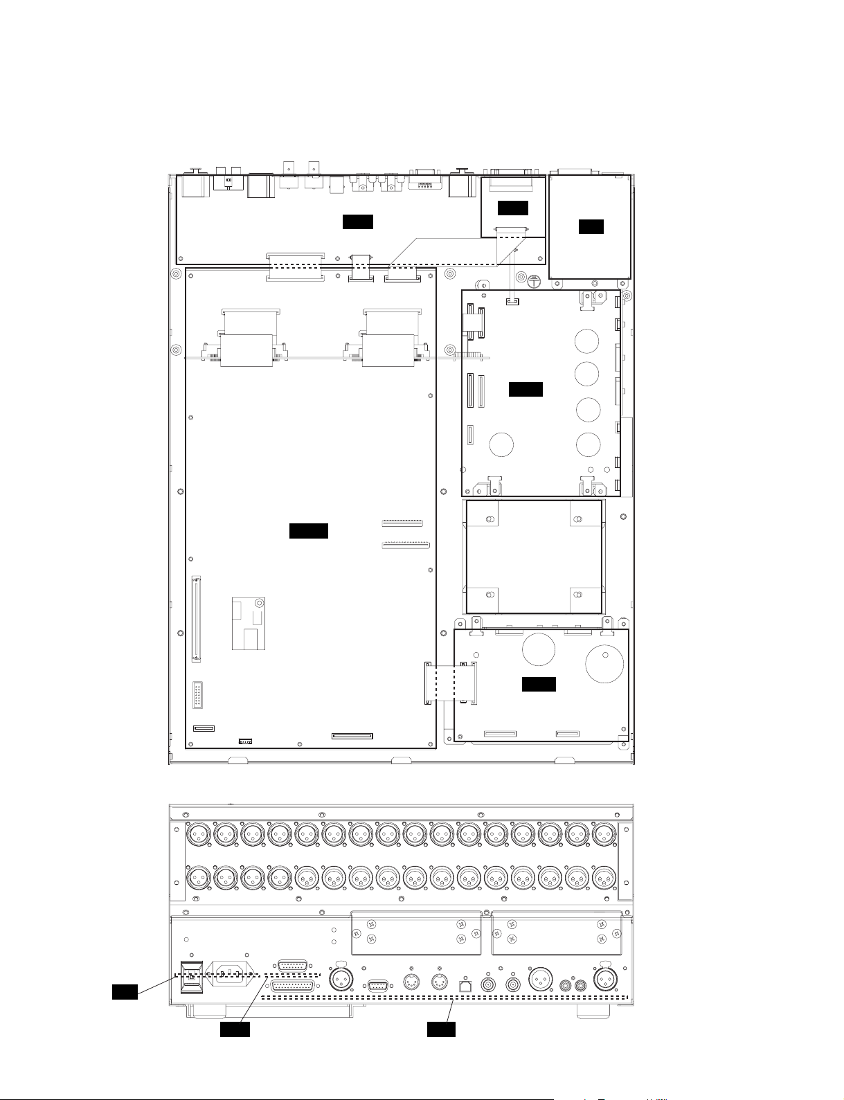
Rear Assembly U Section
17. ADA Circuit Board
(Time required: About 10 minutes)
17-1. Remove the SP1000. (See procedure 1.)
17-2. Remove the MB1000. (See procedure 2.)
17-3. Fasten the control panel assembly. (See procedure 3.)
17-4. Fasten the rear assembly U. (See procedure 4-4.)
17-5. Remove the seven (7) screws marked [30]. The ADA
circuit board can then be removed. (Fig.5)
18. XLR Circuit Board
(Time required: About 18 minutes)
18-1. Remove the SP1000. (See procedure 1.)
18-2. Remove the MB1000. (See procedure 2.)
18-3. Fasten the control panel assembly. (See procedure 3.)
18-4. Fasten the rear assembly U. (See procedure 4-4.)
18-5. Remove the five (5) screws marked [130B]. The XLR
circuit board can then be removed with the rear panel
U. (Fig.6)
18-6. Remove the twenty-four (24) screws marked [110B]
and the forty (40) screws marked [120A]. The XLR
circuit board can then be removed from the rear
panel U. (Fig.6)
リア上 Ass'y 部
17. ADA シート
17-1. SP1000を取り外します。(1項参照)
17-2. MB1000を取り外します。(2項参照)
17-3. コンパネAss'yを固定します。(3項参照)
17-4. リア上Ass'yを固定します。(4-4項参照)
17-5. [30]のネジ7 本を外して、ADAシートを外します。
(図 5)
(所要時間:約 10 分)
18. XLR シート(所要時間:約 18 分)
18-1. SP1000を取り外します。(1項参照)
18-2. MB1000を取り外します。(2項参照)
18-3. コンパネAss'yを固定します。(3項参照)
18-4. リア上Ass'yを固定します。(4-4項参照)
18-5. [130B]のネジ5 本を外して、リアパネル上と共に
XLRシートを外します。(図6)
18-6. [110B]のネジ24本と[120A]のネジ 40 本を外して、
リアパネル上から XLRシートを外します。(図6)
36
ADA
[30]
[30]: Bind Head Tapping Screw-B 3.0X8 MFZN2BL (EP600190)
(+バインドBタイト)
Fig.5 (図5)
Page 37

<Rear view>
)
[120A]
[130B]
<Top view>
Knob x18
(ノブ)
Headt sink
(ヒートシンク)
[120A]
[120A] [120A] [110B] [110B] [110B] [110B]
[120A] [120A] [120A] [120A] [120A] [120A] [120A]
[130B]
[180]
[130B]
[130B]
[110B]
DM1000/MB1000/SP1000
XLR
[110B]
[130B]
[110B]
XLR
[190]
[180]
PC support
(PCサポート
HAAD 2/2
[240A]
[110B]:Bonding Tapping Screw-B 3.0X8 MFZN2BL (VN413300)
[120A]:Bind Head Tapping Screw-B 2.6X8 MFZN2BL (VB096700)
[130B]:Bind Head Tapping Screw-B 4.0X8 MFZN2BL (EG340190)
[180]: Bind Head Tapping Screw-B 3.0X8 MFZN2BL (EP600190)
[190]: Bind Head Screw 4.0X8 MFZN2BL (EG340360)
[240A]:Bind Head Tapping Screw-B 3.0X8 MFZN2BL (EP600190)
(ボンディングBタイト)
(+バインドBタイト)
(+バインドBタイト)
(+バインドBタイト)
(+バインド小ネジ)
(+バインドBタイト)
Fig.6 (図6)
<Top view> <Top view>
Insulation sheet
(放熱シート)
PC support(PCサポート)
HAAD 1/2
Photo.11 (写真11)
Knob x18
(ノブ)
[200]
[200]: Hexagonal nut 9.0 11X2 MFZN2BL (VJ388000)
(特殊六角ナット)
Shield fingers
(接触子)
Photo.12 (写真12)
37
Page 38

DM1000/MB1000/SP1000
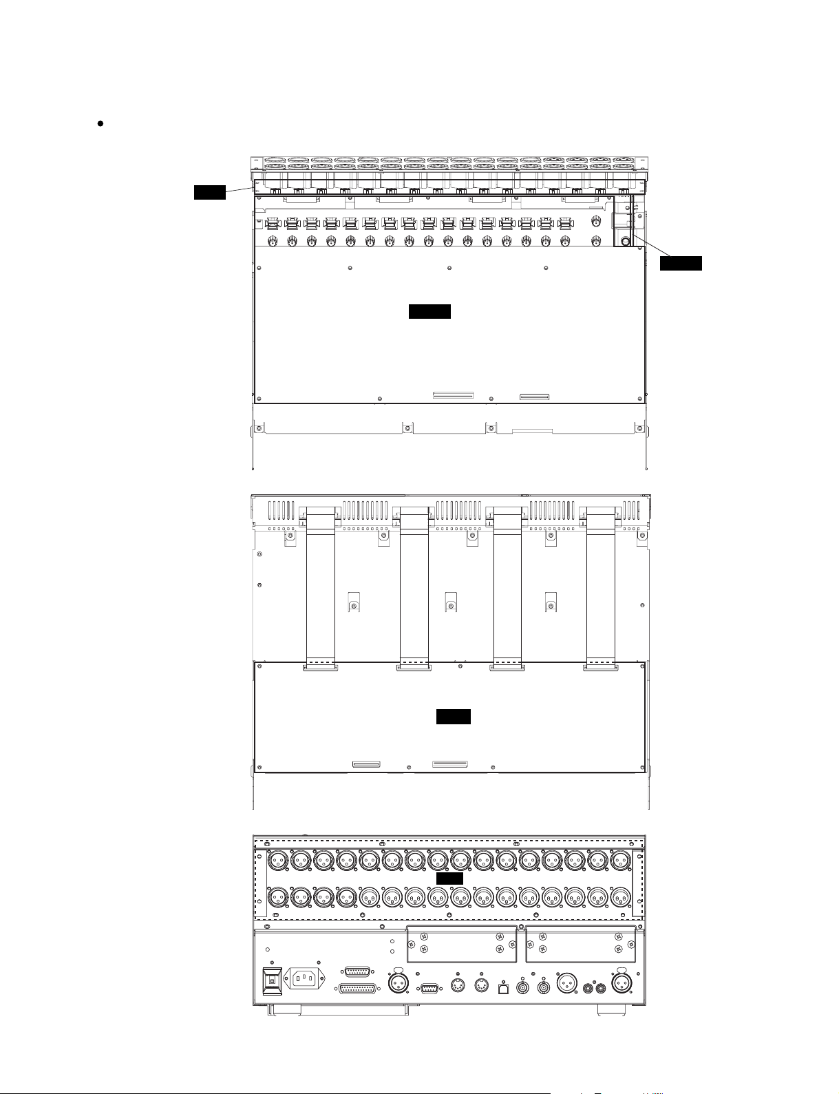
19. Heat Sink (Time required: About 8 minutes)
19-1. Remove the SP1000. (See procedure 1.)
19-2. Remove the MB1000. (See procedure 2.)
19-3. Fasten the control panel assembly. (See procedure 3.)
19-4. Remove the two (2) screws marked [70A]. (Fig.2)
19-5. Remove the four (4) screws marked [240A]. The heat
sink and the insulation sheet can then be removed.
(Fig.6, Photo.11)
20. PC Support (Time required: About 10 minutes)
20-1. Remove the SP1000. (See procedure 1.)
20-2. Remove the MB1000. (See procedure 2.)
20-3. Fasten the control panel assembly. (See procedure 3.)
20-4. Remove the four (4) screws marked [180] and the
eighteen (18) knobs. The PC support and the HAAD
2/2 circuit board can then be removed. (Fig.6,
Photo.12)
The shield fingers attached at the headphone
jack position are attached to the PC support
with double-sided electroconductive tape that
has already been pasted on the part. When
replacing the shield fingers, always replace the
entire part. Please be aware that ordinary
(non-electroconductive) two-sided tape will
not provide adequate performance. (Photo.12)
19. ヒートシンク(所要時間:約 8 分)
19-1. SP1000を取り外します。(1 項参照)
19-2. MB1000を取り外します。(2 項参照)
19-3. コンパネAss'yを固定します。(3 項参照)
19-4. [70A]のネジ2本を外します。(図 2)
19-5. [240A]のネジ 4 本を外して、ヒートシンクと放熱
シートを外します。(図6、写真11)
20. PC サポート(所要時間:約 10 分)
20-1. SP1000を取り外します。(1 項参照)
20-2. MB1000を取り外します。(2 項参照)
20-3. コンパネAss'yを固定します。(3 項参照)
20-4. [180]のネジ 4 本とノブ 18 個を外して、PCサポート
と HAAD2/2シートを外します。(図 6、写真 12)
※ヘッドフォンジャック部の接触子は、貼付済みの
導電性両面テープでPC サポートに取り付けられ
ています。接触子を交換する時は、かならず部品
ごと交換してください。普通の両面テープでは性
能が得られませんのでご注意ください。(写真12)
21. HAAD 2/2 Circuit Board
(Time required: About 11 minutes)
21-1. Remove the SP1000. (See procedure 1.)
21-2. Remove the MB1000. (See procedure 2.)
21-3. Fasten the control panel assembly. (See procedure 3.)
21-4. Remove the PC support. (See procedure 20.)
21-5. Remove the screw marked [190] and the hexagonal
nut marked [200]. The HAAD 2/2 circuit board can
then be removed. (Fig.6, Photo.12)
22. HAAD 1/2 Circuit Board
(Time required: About 13 minutes)
22-1. Remove the SP1000. (See procedure 1.)
22-2. Remove the MB1000. (See procedure 2.)
22-3. Fasten the control panel assembly. (See procedure 3.)
22-4. Remove the heat sink. (See procedure 19.)
22-5. Remove the PC support. (See procedure 20.)
22-6. Remove the eight (8) screws marked [60C]. The
HAAD 1/2 circuit board can then be removed. (Fig.7)
22-7. Remove the eighteen (18) spacers and the button
assemblies from the HAAD 1/2 circuit board.
(Photo.13)
21. HAAD2/2 シート(所要時間:約 11 分)
21-1. SP1000を取り外します。(1 項参照)
21-2. MB1000を取り外します。(2 項参照)
21-3. コンパネAss'yを固定します。(3 項参照)
21-4. PCサポートを取り外します。(20 項参照)
21-5. [190]のネジ1 本と[200]の特殊六角ナット 1 個を外
して、HAAD2/2 シートを外します。(図 6、写真 12)
22. HAAD1/2 シート(所要時間:約 13 分)
22-1. SP1000を取り外します。(1 項参照)
22-2. MB1000を取り外します。(2 項参照)
22-3. コンパネAss'yを固定します。(3 項参照)
22-4. ヒートシンクを取り外します。(19項参照)
22-5. PCサポートを取り外します。(20 項参照)
22-6. [60C]のネジ8本を外して、HAAD1/2シートを外
します。(図7)
22-7. HAAD1/2シートから、ノブスペーサー18個とボ
タン Ass'y16個を外します。(写真 13)
38
Page 39

[
]
<Top view>
HAAD 1/2
DM1000/MB1000/SP1000
<Top view>
HAAD 1/21/2
HAAD 2/2
Button assembly x16
(ボタンAss'y)
Knob spacer x18
(ノブスペーサー)
Photo.13 (写真13)
60C
Control Panel Assembly Section
When removing the circuit board, if it is hard to handle
while the control panel assembly is fixed slantwise
at the stay, open it widely at 180° for the work.
23. FD Circuit Board
(Time required: About 9 minutes)
23-1. Remove the SP1000. (See procedure 1.)
23-2. Remove the MB1000. (See procedure 2.)
23-3. Remove the seventeen (17) fader knobs from the
control panel side. (Fig.8)
23-4. Fasten the control panel assembly. (See procedure 3.)
23-5. Remove the ten (10) screws marked [260]. The FD
circuit board can then be removed with the insulation
sheet. (Fig.9)
23-6. Remove the four (4) cord holders. The insulation
sheet can then be removed from the FD circuit board.
(Fig.9)
The insulation sheet is fastened to the FD circuit
board by the cord holders.
When you replace the FD circuit board, be sure to
attach the insulation sheet as before.
[60C]: Bind Head Tapping Screw-B
3.0X8 MFZN2BL (EP600190)
(+バインドBタイト)
Fig.7 (図7)
コンパネ Ass'y 部
※シートを取り外す時に、ステイでコンパネAss'yを45度
程度に固定した状態で作業がしにくい場合は、180度開
いて作業をしてください。
23. FD シート(所要時間:約 9 分)
23-1. SP1000 を取り外します。(1 項参照)
23-2. MB1000 を取り外します。(2 項参照)
23-3. コントロールパネル面より、フェーダーノブ 17 個
を外します。(図8)
23-4. コンパネ Ass'y を固定します。(3 項参照)
23-5. [260]のネジ10本を外して、絶縁シートと共に FD
シートを外します。(図9)
23-6. インシュロックタイ 4 本を外して、FDシートから
絶縁シートを外します。(図9)
※絶縁シートは、インシュロックタイでFDシート
に固定されています。
※FDシートを交換する際は、絶縁シートを必ず元
通りに取り付けてください。
39
Page 40

DM1000/MB1000/SP1000
24. LCD Circuit Board
(Time required: About 8 minutes)
24-1. Remove the SP1000. (See procedure 1.)
24-2. Remove the MB1000. (See procedure 2.)
24-3. Fasten the control panel assembly. (See procedure 3.)
24-4. Remove the two (2) screws marked [120B] and the
two (2) screws marked [170]. The LCD circuit board
can then be removed with the LCD shield film and
the LCD shield plate. (Photo.15)
24-5. Remove the two (2) screws marked [120C]. The LCD
circuit board can then be removed. (Photo.16)
25.
PN1 (1/4), (2/4 Meter), (3/4 Joystick) a n d (4/4 Encoder) C i r cuit Boar ds
25-1. Remove the SP1000. (See procedure 1.)
25-2. Remove the MB1000. (See procedure 2.)
25-3. Fasten the control panel assembly. (See procedure 3.)
25-4. Remove the FD circuit board. (See procedure 23.)
25-5. PN1 (3/4 Joystick) Circuit Board
(Time required: About 9 minutes):
Remove the three (3) screws marked [218]. The PN1
(3/4 joystick) circuit board can then be removed.
(Fig.9)
25-6. PN1 (4/4 Encoder) Circuit Board
(Time required: About 10 minutes):
a. Remove the three (3) screws marked [220A]. The
PN1 (4/4 encoder) circuit board can then be removed
with the encoder knob. (Fig.9, photo.14)
b. Remove the encoder knob and the hexagonal nut.
The encoder angle bracket can then be removed
from the PN1 (4/4 encoder). (photo.14)
25-7. PN1 (2/4 Meter) Circuit Board
(Time required: About 10 minutes):
a. Remove the LCD shield plate. (See procedure 24-4.)
b. Remove the two (2) screws marked [120D]. The PN1
(2/4 meter) circuit board can then be removed. (Fig.9)
25-8. PN1 (1/4) Circuit Board
(Time required: About 12 minutes):
a. Remove the three (3) encoder knobs marked [300],
the sixteen (16) encoder knobs marked [310] and
the knob marked [350B] from the control panel side.
(Fig. 8)
b. Remove the PN1 (4/4 encoder) circuit board.
(See procedure 25-6-a.)
c. Remove the fourteen (14) screws marked [220B].
The PN1 (1/4) circuit board can then be removed.
(Fig. 9)
24. LCD シート(所要時間:約 8 分)
24-1. SP1000を取り外します。(1項参照)
24-2. MB1000を取り外します。(2項参照)
24-3. コンパネAss'yを固定します。(3項参照)
24-4. [120B]のネジ2本と[170]のネジ2本を外して、LCD
シールドフィルムとLCD シールド板と共に L C D
シートを外します。(写真15)
24-5. [120C]のネジ2本を外して、LCDシートを外しま
す。(写真16)
25. PN1(1/4)、(2/4メーター)、(3/4ジョイス
ティック)、(4/4エンコーダー)シート
25-1. SP1000を取り外します。(1項参照)
25-2. MB1000を取り外します。(2項参照)
25-3. コンパネAss'yを固定します。(3項参照)
25-4. FDシートを外します。(23項参照)
25-5. PN1(3/4ジョイスティック)シート
(所要時間:約 9分):
[218]のネジ 3 本を外して、PN1 (3/4ジョイス
ティック)シートを外します。(図9)
25-6. PN1(4/4エンコーダー)シート
(所要時間:約 10分):
a. [220A]のネジ3本を外して、エンコーダーツマミと
共にPN1(4/4 エンコーダー) シートを外します。
(図 9、写真14)
b. エンコーダーツマミと特殊六角ナットを外して、
PN1(4/4エンコーダー)シートからエンコーダーア
ングルを外します。(写真14)
25-7. PN1(2/4メーター)シート(所要時間:約10分):
a. LCD シールド板を外します。(24-4項参照)
b. [120D]のネジ2 本を外して、PN1 (2/4メーター)
シートを外します。(図9)
25-8. PN1(1/4)シート(所要時間:約12分):
a. コントロールパネル面より、[300]のエンコーダーノ
ブ3個と[310]のエンコーダーノブ16個、[350B]のノ
ブ 1個を外します。(図8)
b. PN1(4/4エンコーダー)シートを外します。
(25-6-a 項参照)
c. [220B]のネジ14本を外して、PN1(1/4)シートを外
します。(図9)
26. PN2 Circuit Board
(Time required: About 8 minutes)
26-1. Remove the SP1000. (See procedure 1.)
26-2. Remove the MB1000. (See procedure 2.)
26-3. Fasten the control panel assembly. (See procedure 3.)
26-4. Remove the five (5) screws marked [240B]. The PN2
circuit board can then be removed. (Fig.9)
40
26. PN2 シート(所要時間:約8分)
26-1. SP1000を取り外します。(1項参照)
26-2. MB1000を取り外します。(2項参照)
26-3. コンパネAss'yを固定します。(3項参照)
26-4. [240B]のネジ5本を外して、PN2シートを外します。
(図 9)
Page 41

)
<Top view>
DM1000/MB1000/SP1000
[300]:
Encoder knob
(エンコーダーノブ)
Knob(ノブ)
[350B]:
[310]: Encoder knob x16
(エンコーダーノブ)
Encoder knob
(エンコーダーツマミ
Fader knob x17
(フェーダーノブ)
Fig.8 (図8)
41
Page 42

DM1000/MB1000/SP1000
<Bottom view>
[220B]
[120D]
PN1
(2/4 Meter)
[220B]
PN1
(3/4 Joystick)
[218]
PN1
[220A]
(4/4 Encoder)
Encoder angle bracket
(エンコーダーアングル)
[220A]
Cord holder
(インシュロックタイ)
[220B]
[240B]
PN2
PN1 (1/4)(1/4)
FD
LCD
[220B]
Cord holder
(インシュロックタイ)
Insulation sheet
(絶縁シート)
Encoder angle bracket
(エンコーダーアングル)
Hexagonal nut
(特殊六角ナット)
Photo.14 (写真14)
42
Cord holder
(インシュロックタイ)
Encoder knob
(エンコーダーツマミ)
Cord holder
(インシュロックタイ)
[260]
[120B]: Bind Head Tapping Screw-B 3.0X8 MFZN2BL (EP600190)
[218]: Bind Head Tapping Screw-B 3.0X6 MFZN2BL (EP600230)
[220]: Bind Head Tapping Screw-B 3.0X8 MFZN2BL (EP600190)
[240B]: Bind Head Tapping Screw-B 3.0X8 MFZN2BL (EP600190)
[260]: Bind Head Tapping Screw-B 3.0X8 MFZN2BL (EP600190)
(+バインドBタイト)
(+バインドBタイト)
(+バインドBタイト)
(+バインドBタイト)
(+バインドBタイト)
Fig.9 (図9)
Page 43

DM1000/MB1000/SP1000
<Bottom view> <Bottom view>
<Bottom view>
LCD
LCD shield plate
(LCDシールド板)
LCD
(液晶ディスプレイ)
LCD shield film
(LCDシールドフィルム)
[120B]
[170]
[80]
[80] [80]
[120C]
[F] (four (4) places)
PN1 2/4
27. LCD (Time required: About 10 minutes)
27-1. Remove the SP1000. (See procedure 1.)
27-2. Remove the MB1000. (See procedure 2.)
27-3. Fasten the control panel assembly. (See procedure 3.)
27-4. Remove the LCD shield plate. (See procedure 24-4.)
27-5. Remove the PN1 (2/4 meter) circuit board.
(See procedure 25-7.)
27. 液晶ディスプレイ(所要時間:約 10 分)
27-1. SP1000 を取り外します。(1 項参照)
27-2. MB1000 を取り外します。(2 項参照)
27-3. コンパネ Ass'y を固定します。(3 項参照)
27-4. LCD シールド板を取り外します。(24-4 項参照)
27-5. PN1(2/4メーター)シートを外します。(25-7項参照)
27-6. [80]のネジ4本を外して、液晶ディスプレイを外し
27-6. Remove the four (4) screws marked [80]. The LCD
can then be removed. (Photo.17)
When you install the LCD shield plate, be sure to
put the four (4) places marked [F] of the LCD
shield plate into the slot of the LCD case.
(Photo.16, 18)
ます。(写真17)
※LCD シールド板を取り付ける時は、LCDシール
ド金具の4ケ所の[F]の部分をLCDケースの溝に
入れてください。(写真16、18)
[120B]: Bind Head Tapping Screw-B 3.0X8 MFZN2BL (EP600190)
[170]: Bind Head Tapping Screw-B 3.0X8 MFZN2BL (EP600190)
(+バインドBタイト)
(+バインドBタイト)
Photo.15 (写真15)
[80]: Bind Head Tapping Screw-B 2.6X6 MFZN2BL (V8927300)(+バインドBタイト)
Photo.17 (写真17)
Photo.16 (写真16)
Photo.18 (写真18)
[120C]: Bind Head Tapping Screw-B
3.0X8 MFZN2BL (EP600190)
(+バインドBタイト)
43
Page 44

DM1000/MB1000/SP1000
Disassembling the MB1000
28. Rear Panel
28-1. Remove the MB1000. (See procedure 2.)
28-2. Remove the sixteen (16) screws marked [40C]. The
rear panel can then be removed from the front panel.
(Fig.10)
(Time required: About 3 minutes)
29. PN Circuit Board
(Time required: About 4 minutes)
29-1. Remove the MB1000. (See procedure 2.)
29-2. Remove the rear panel. (See procedure 28.)
29-3. Remove the six (6) screws marked [50]. The PN
circuit board can then be removed. (Photo.19)
30. MAIN Circuit Board
(Time required: About 4 minutes)
30-1. Remove the MB1000. (See procedure 2.)
30-2. Remove the rear panel. (See procedure 28.)
30-3. Remove the six (6) screws marked [70B]. The MAIN
circuit board can then be removed. (Photo.19)
31. DSUB Cable (Time required: About 4 minutes)
31-1. Remove the MB1000. (See procedure 2.)
31-2. Remove the rear panel. (See procedure 28.)
31-3. Remove the screw marked [70C]. The cable holder
can then be removed. (Photo.19)
31-4. Remove the bushing from the rear panel. (Photo .20)
31-5. Remove the DSUB cable and the bushing from the
rear panel. (Photo.19)
The bushing is not part of the DSUB cable.
When you replace the DSUB cable, you should
remove the bushing from the cable, and attach
in the new cable.
MB1000 の分解
28. リアパネル
28-1. MB1000を取り外します。(2項参照)
28-2. [40C]のネジ16本を外して、フロントパネルからリ
アパネルを外します。(図10)
(所要時間:約 3 分)
29. PN シート(所要時間:約4分)
29-1. MB1000を取り外します。(2項参照)
29-2. リアパネルを外します。(28項参照)
29-3. [50]のネジ6本を外して、PNシートを外します。
(写真 19)
30. MAIN シート(所要時間:約 4 分)
30-1. MB1000を取り外します。(2項参照)
30-2. リアパネルを外します。(28項参照)
30-3. [70B]のネジ6本を外して、MAINシートを外しま
す。(写真19)
31. DSUB ケーブル(所要時間:約 4 分)
31-1. MB1000を取り外します。(2項参照)
31-2. リアパネルを外します。(28項参照)
31-3. [70C]のネジ1本を外して、ケーブルホルダーを外
します。(写真19)
31-4. ワンタッチブッシュをリアパネルから外します。
(写真 20)
31-5. ワンタッチブッシュとDSUBケーブルをリアパネ
ルから外します。(写真19)
※ワンタッチブッシュはDSUBケーブルの構成部品
ではありません。DSUBケーブルを交換する際に
は、ケーブルからワンタッチブッシュを取り外し
て、新しいケーブルに取り付けてください。
44
Page 45

DM1000/MB1000/SP1000
)
<Front view>
<Rear view>
Front panel
(フロントパネル)
Rear panel(リアパネル)
<Left side view>
<Right side view>
<Bottom view>
[40C]
[40C]
[40C]
[40C]: Bind Head Tapping Screw-B 3.0X8 MFZN2BL (EP600190)
(+バインドBタイト)
Fig.10 (図10)
<Rear view>
[50]
PN
MAIN
<Front view>
Meter angle R
(メーターアングルR)
[70B]
Meter angle L
(メーターアングルL)
DSUB cable
(DSUBケーブル)
[50]: Bind Head Tapping Screw-B 3.0X8 MFZN2BL (EP600190)
[70]: Bind Head Tapping Screw-B 3.0X8 MFZN2BL (EP600190)
(+バインドBタイト)
(+バインドBタイト)
Cable holder
(ケーブルホルダー)
[70C]
Bushing
(ワンタッチブッシュ
Photo.20 (写真20)
Photo.19 (写真19)
45
Page 46

DM1000/MB1000/SP1000
W
O
R
D C
L
O
C
K
IN
O
U
T
C
O
N
T
R
O
L
IN
O
U
T
T
O
H
O
S
T
U
S
B
R
E
M
O
T
E
M
ID
I
S
M
P
T
E
I
N
C
O
A
X
IA
L
A
E
S
/
E
B
U
C
O
A
X
I
A
L
A
E
S
/E
B
U
2
2
1
2
T
R
IN
D
IG
IT
AL
M
E
T
E
R
P
O
W
E
R
O
N
O
F
F
1
S
L
O
T
S
L
O
T
IN
P
U
T
O
M
N
I
IN
23
4
56
78
1
10
111213
14
5
9
234
5
67
8
1
10
11
12
9
2
1
3
D
I
G
IT
A
L
M
IX
IN
G
C
O
N
S
O
L
E
M
O
D
E
L
D
M
1
0
0
0
A
C
IN
W
O
R
D
C
L
O
C
K
IN
O
U
T
CONTROL
IN
O
U
T
T
O
H
O
S
T
U
S
B
R
E
M
O
T
E
M
ID
I
SMPTE IN
C
O
A
X
IA
L
A
E
S
/E
B
UC
O
A
X
IA
L
A
E
S
/
E
B
U
2
2
1
2
T
R
IN
D
IG
IT
A
L
M
E
T
E
R
P
OW
E
R
O
N
O
F
F
1
S
L
O
T
S
L
O
T
IN
P
U
T
O
M
N
I
IN
23
4
56
7
8
1
10
1112
13
145
9
23
4
5678
1
10
1112
9
2
1
3
D
IG
IT
A
L
M
IX
IN
G
C
O
N
S
O
L
E
M
O
D
E
L
D
M
1
0
0
0
A
C I
N
INSTALLING AN OPTIONAL CARD
Follow the steps below to install an optional mini-YGD AI
card.
1 Make sure that the power to the DM1000 is turned off.
2 Undo the two fixing screws and remove the slot
cover, as shown below.
Keep the cover and fixing screws in a safe place for
future use.
(オプションカードの取り付け)
オプションのmini‐YGDAIカードは次のように取り付
けます。
1 DM1000の電源がオフになっていることを確認します。
2 スロットの固定ネジをゆるめ、スロットカバーを取り
外します。
取り外したスロットカバーは、安全な場所に保管して
ください。
3 Insert the card between the guide rails and slide it
all the way into the slot, as shown below.
You may have to push firmly to fully insert the card into
the internal connector.
4 Secure the card using the attached thumbscrews.
Tighten the screws firmly, or else the card may not be
grounded correctly, which may cause the DM1000 to
malfunction.
46
3 スロット内のガイドレールにカードの両端を合わせ、
カードをスロットに挿入します。
このとき、カードの端子部分がスロット内部の端子に
正しくはまるようカードをいっぱいまで押し込んでく
ださい。
4 カードに取り付けられているネジでカードを固定します。
カードが固定されていないと、故障や誤動作の原因と
なることがありますのでご注意ください。
Page 47

DM1000/MB1000/SP1000
LSI PIN DESCRIPTION
DM1000
(LSI端子機能表)
M37641M8-141FP (X2485200) CPU (USB 32K) ..........................................................................47
HD6417709SF133 (X2081A00) CPU (SH-3) .................................................................................48
SH7042 (X4409A00) CPU (SUB)...................................................................................................49
MBCG46183-129PFV-G (XV833A00) Gate Array (SIO4) ............................................................50
SGH603064F-62F (XV973A00) Gate Array .................................................................................. 50
YSS910-S (XV988A00) DSP6 (Digital Signal Processor) ........................................................... 51
YSS919B-H (XZ693B00) DSP7 (Digital Signal Processor).........................................................52
MBCG61594-130 (X3299A00) ATSC2A .......................................................................................53
YM3436DK (XG948E00) DIR2 (Digital Format Interface Receiver) ...........................................54
CS8405A-CS (XZ349A00) DIT (Digital Audio Interface Transmitter)........................................ 54
S1D13704F00A100 (X3498A00) LCDC (LCD Controller)............................................................55
CS8420 (XW559A00) SRC (Sample Rate Converter) .................................................................55
ICS2008BV-T (X2832B00) T.C. Reader/Generator.....................................................................56
AK4393-VF-E2 (XW029A00) DAC (Digital to Analog Converter) ..............................................56
CS5361-KS (X3447A00) ADC (Analog to Digital Converter) .....................................................56
MB1000
SH7042 (X4409A00) CPU (SH-2) ..................................................................................................57
M37641M8-141FP (X2485200) CPU (USB 32K)
PIN
NO.
1
P61/DQ
2
P60/DQ
3
P57//W/(R//W)
4
P56//R(E)
5
6
7
P53//IBF
8
P52/OBF
9
CNVSS/V
10
/RESET
11
P51/T
12
P50/X
13
14
15
16
17
18
19
20
P44/CNTR
21
P43/CNTR
22
P42/INT
23
P41/INT
24
P40//EDMA
25
P87//RTS
26
P86//CTS
27
P85/URXD
28
P84/UTXD
29
P83//RTS2/STXD
30
P8
31
P81/URXD2/SCLK
32
P8
33
P37//RD
34
P3
35
P35/SYNC
36
P34/Ø
37
P33/DMA
38
39
40
P30/RDY
NAME
P5
P54//S
V
X
X
V
AV
LPF
AV
2
//CTS2/SRXD
0
/UTXD2//SRDY
6
P3
P3
5/A0
OUT
/XC
SS
IN
OUT
CC
CC
SS
//WR
2
1
CIN
OUT
0
PP
OUT
OUT
OUT
I/O
1
I/O
0
I/O
Port 6
FUNCTION
I/O
I/O
I/O
I/O
0
I/O
0
I/O
I/O
I/O
Port 5
I
Chip operation mode
I
Reset input
Port 5
Ground
I
O
Quartz crystal input
Quartz crystal output
Power supply +5V
Analog power supply +5V
O
Loop filter for synthesizer
Analog ground
1
I/O
0
I/O
1
I/O
0
I/O
Port 4
I/O
1
I/O
1
I/O
1
I/O
1
I/O
I/O
Port 8
I/O
I/O
I/O
I/O
I/O
I/O
I/O
I/O
Port 3
I/O
I/O
I/O
PIN
NO.
41
P17/AB
42
P16/AB
43
P15/AB
44
P14/AB
45
P13/AB
46
P12/AB
47
P11/AB
48
P10/AB
49
P07/AB
50
P06/AB
51
P05/AB
52
P04/AB
53
P03/AB
54
P02/AB
55
P01/AB
56
P00/AB
57
P27/DB
58
P26/DB
59
P25/DB
60
P24/DB
61
P23/DB
62
P22/DB
63
P21/DB
64
P20/DB
65
P74/OBF
66
P73//IBF1//HLDA
67
68
P71//HOLD
69
P70//SOF
70
USB D+
71
USB D-
72
Ext. Cap
73
74
75
P67/DQ
76
P66/DQ
77
P65/DQ
78
P64/DQ
79
P63/DQ
80
P62/DQ
NAME
P72//S
V
SS
V
CC
I/O
15
I/O
I/O
14
I/O
13
I/O
12
I/O
11
I/O
10
I/O
9
I/O
8
I/O
7
I/O
6
I/O
5
I/O
4
I/O
3
I/O
2
I/O
1
I/O
0
I/O
7
I/O
6
I/O
5
I/O
4
I/O
3
I/O
2
I/O
1
I/O
0
I/O
1
Port 1
Port 0
Port 2
FUNCTION
I/O
I/O
1
Port 7
I/O
I/O
I/O
I/O
I/O
USB +voltage line interface
USB -voltage line interface
Power supply +3.3V
Ground
Power supply +5V
I/O
7
I/O
6
I/O
5
I/O
4
I/O
3
I/O
2
Port 6
JK1: IC102
47
Page 48

DM1000/MB1000/SP1000
HD6417709SF133 (X2081A00) CPU (SH3)
PIN
NAME
NO.
1
MD1
2
MD2
3
Vcc(RTC)
4
XTAL2
5
EXTAL2
6
Vss(RTC)
7
NMI
IRQ0/IRL0/PTH0
8
IRQ1/IRL1/PTH1
9
IRQ2/IRL2/PTH2
10
IRQ3/IRL3/PTH3
11
IRQ4/PTH4
12
D31/PTB7
13
D30/PTB6
14
D29/PTB5
15
D28/PTB4
16
D27/PTB3
17
D26/PTB2
18
VssQ
19
D25/PTB1
20
VccQ
21
D24/PTB0
22
D23/PTA7
23
D22/PTA6
24
D21/PTA5
25
D20/PTA4
26
27
D19/PTA3
28
29
D18/PTA2
30
D17/PTA1
31
D16/PTA0
32
VssQ
33
D15
34
VccQ
35
D14
36
D13
37
D12
38
D11
39
D10
40
41
42
43
44
VssQ
45
46
VccQ
47
48
49
50
51
52
53
54
55
56
VssQ
57
58
VccQ
59
60
61
62
63
64
A10
65
A11
66
A12
67
A13
68
VssQ
69
A14
70
VccQ
71
A15
72
A16
73
A17
74
A18
75
A19
76
A20
77
A21
78
79
A22
80
81
A23
82
VssQ
83
A24
84
VccQ
85
A25
86
BS/PTK4
87
88
WE0/DQMLL
89
WE1/DQMLU/WE
90
WE2/DQMUL/ICIORD/PTK6
91
WE3/DQMUU/ISIOWR/PTK7
92
RD/WR
93
AUDSYNC/PTE7
94
VssQ
95
CS0/MCS0
96
VccQ
97
CS2/PTK0
98
CS3/PTK1
99
CS4/PTK2
100
CS5/CE1A/PTK3
101
CS6/CE1B
102
CE2A/PTE4
103
CE2B/PTE5
104
Vss
Vcc
D9
D8
D7
D6
D5
D4
D3
D2
D1
D0
A0
A1
A2
A3
A4
A5
A6
A7
A8
A9
Vss
Vcc
RD
I/O
I/O
I/O
I/O
I/O
I/O
I/O
I/O
I/O
I/O
I/O
I/O
I/O
I/O
I/O
I/O
I/O
I/O
I/O
I/O
I/O
I/O
I/O
I/O
I/O
I/O
I/O
I/O
I/O
I/O
I/O
I/O
I/O
I/O
I/O
I/O
I/O
I/O
I/O
I/O
I/O
I/O
I/O
I
I
-
O
I
I
I
I
I
I
I
-
-
-
-
-
-
-
-
O
O
O
O
-
O
O
O
O
O
O
O
O
O
O
O
O
O
O
O
O
O
O
O
O
O
O
O
O
O
O
O
-
O
Mode control
Power supply +1.8 V
Crystal oscillator
Ground
Non-maskable interrupt request
Interrupt request / Port H
Data bus / Port B
Ground
Data bus / Port B
Power supply +3.3 V
Data bus / Port B
Data bus / Port A
Ground
Data bus / Port A
Power supply +1.8 V
Data bus / Port A
Ground
Data bus
Power supply +3.3 V
Data bus
Ground
Data bus
Power supply +3.3 V
Data bus
Address bus
Ground
Address bus
Power supply +3.3 V
Address bus
Ground
Address bus
Power supply +3.3 V
Address bus
Ground
Address bus
Power supply +1.8 V
Address bus
Ground
Address bus
Power supply +3.3 V
Address bus
Bus cycle / Port K
Read strobe
Select signal (D7-D0) / D QM (SDRAM)
Select signal (D15-D8) / D QM (SDRAM) / Write enable
Select signal (D23-D16) / D QM (SDRAM) / I/O read / Port K
Select signal (D31-D24) / D QM (SDRAM) / I/O write / Port K
Read / Write
AUD cycle / Port E
Ground
Chip select / Mask ROM chip select
Power supply +3.3V
Chip select / Port K
Chip select / Chip enable / Port K
Chip select / Chip enable
Chip enable / Port E
FUNCTION
PIN
NAME
NO.
105
CKE/PTK5
RAS3L/PTJ0
106
PTJ1
107
CASL/PTJ2
108
VssQ
109
CASU/PTJ3
110
VccQ
111
PTJ4
112
PTJ5
113
DACK0/PTD5
114
DACK1/PTD7
115
PTE6
116
PTE3
117
RAS3U/PTE2
118
PTE1
119
TDO/PTE0
120
BACK
121
BREQ
122
WAIT
123
RESETM
124
ADTRG/PTH5
125
IOIS16/PTG7
126
ASEMD0/PTG6
127
ASEBRKAK/PTG5
128
PTG4/CKIO2
129
AUDATA3/PTG3
130
AUDATA2/PTG2
131
Vss
132
AUDATA1/PTG1
133
Vcc
134
AUDATA0/PTG0
135
TRST/PTF7/PINT15
136
TMS/PTF6/PINT14
137
TDI/PTF5/PINT13
138
TCK/PTF4/PINT12
139
IRLS3/PTF3/PINT11
140
IRL2/PTF2/PINT10
141
IRLS1/PTF1/PINT9
142
IRLS0/PTF0/PINT8
143
MD0
144
Vcc(PLL1)
145
CAP1
146
Vss(PLL1)
147
Vss(PLL2)
148
CAP2
149
VCC(PLL2)
150
AUDCK/PTH6
151
Vss
152
Vss
153
Vcc
154
XTAL1
155
EXTAL1
156
STATUS0/PTJ6
157
STATUS1/PTJ7
158
TCLK/PTH7
159
/IRQOUT
160
VssQ
161
CKIO
162
VccQ
163
TXD0/SCPT0
164
SCK0/SCPT1
165
TXD1/SCPT2
166
SCK1/SCPT3
167
TXD2/SCPT4
168
SCK2/SCPT5
169
RTS2/SCPT6
170
RXD0/SCPT0
171
RXD1/SCPT2
172
Vss
173
RXD2/SCPT4
174
Vcc
175
CTS2/IRQ5/SCPT7
176
MCS7/PTC7/PINT7
177
MCS6/PTC6/PINT6
178
MCS5/PTC5/PINT5
179
MCS4/PTC4/PINT4
180
VssQ
181
WAKEUP/PTD3
182
VccQ
183
RESETOUT/PTD2
184
MCS3/PTC3/PINT3
185
MCS2/PTC2/PINT2
186
MCS1/PTC1/PINT1
187
MCS0/PTC0/PINT0
188
DRAK0/PTD1
189
DRAK1/PTD0
190
DREQ0/PTD4
191
DREQ1/PTD6
192
RESETP
193
CA
194
MD3
195
MD4
196
MD5
197
AVss
198
AN0/PTL0
199
AN1/PTL1
200
AN2/PTL2
201
AN3/PTL3
202
AN4/PTL4
203
AN5/PTL5
204
AVcc
205
AN6/DA1/PTL6
206
AN7/DA0/PTL7
207
AVss
208
I/O
I/O
I/O
I/O
I/O
I/O
I/O
I/O
I/O
I/O
I/O
I/O
I/O
I/O
I/O
I/O
I/O
I/O
I/O
I/O
I/O
I/O
I/O
I/O
I/O
I/O
I/O
I/O
I/O
I/O
I/O
I/O
I/O
I/O
I/O
I/O
I/O
I/O
I/O
I/O
I/O
I/O
MAIN: IC001
I/O
CK enable / Port K
RAS address bus / Port J
Port J
-
-
O
I
I
I
I
I
I
-
I
I
I
I
I
I
I
I
I
-
-
-
-
-
I
-
-
-
O
I
O
-
-
O
O
O
I
I
I
I
-
-
I
I
I
I
I
I
I
I
I
I
I
I
I
-
-
CAS address bus / Port J
Ground
CAS address bus / Port J
Power supply +3.3 V
Port J
DMA acknowledge / Port D
Port E
RAS address bus / Port E
Port E
Test data / Port E
Bus acknowledge
Bus request
Hardware wait request
Manual reset
Analog trigger / Port H
Write protect / Port G
ASE mode / Port G
ASE break acknowledge / Port G
Port G / Clock output
AUD data / Port G
Ground
AUD data / Port G
Power supply +1.8 V
AUD data / Port G
Test reset / Port F / Port interruption
Test mode switch / Port F / Port interruption
Test data / Port F / Port interruption
Test clock / Port F / Port interruption
Interrupt request / Port F / Port interruption
Mode control
Power supply +1.8 V
Capacitor
Ground
Ground
Capacitor
Power supply +1.8 V
AUD clock / Port H
Ground
Power supply +1.8 V
Crystal oscillator
Processor status / Port J
Timer clock / Port H
Interrupt request output
Ground
System clock input / output
Power supply +3.3 V
Data transmission / SCI port
Serial clock / SCI port
Data transmission / SCI port
Serial clock / SCI port
Data transmission / SCI port
Serial clock / SCI port
Transmit request / SCI port
Data reception / SCI port
Ground
Data reception / SCI port
Power supply +1.8 V
Transmit clear / Interrupt request / SCI port
Mask ROM chip select / Port C / Port interruption
Ground
Standby mode Interrupt request output / Port D
Power supply +3.3 V
Reset output / Port D
Mask ROM chip select / Port C / Port interruption
DMA acknowledge / Port D
DMA request / Port D
Power on reset
Chip active
Mode control
Analog ground
Analog input / Port L
Analog power supply +3.3 V
Analog input / Analog output / Port L
Analog ground
FUNCTION
48
Page 49

DM1000/MB1000/SP1000
SH7042 (X4409A00) CPU (SUB)
PIN
NO.
1
2
3
4
5
6
7
8
9
10
11
12
13
14
15
16
17
18
19
20
21
22
23
24
25
26
27
28
29
30
31
32
33
34
35
36
37
38
39
40
41
42
43
44
45
46
47
48
49
50
51
52
53
54
55
56
PE14
PE15
VSS
A10
A11
A12
A13
A14
A15
A16
VCC
A17
VSS
PB2//RQ0
PB3//RQ1
PB4//RQ2
VSS
PB5//RQ3
A18
A19
A20
PB9
VSS
/WDTOVF
/WRH
VCC
/WRL
VSS
/CS1
/CS0
PA9//IRQ3
PA8//IRQ2
/CS3
/CS2
PA5//IRQ1
TXD1
RXD1
IRQ0
TXD0
PA0
D15
D14
D13
VSS
D12
A0
A1
A2
A3
A4
A5
A6
A7
A8
A9
/RD
I/O FUNCTIONNAME
I/O
I/O
I/O
I/O
O
O
I
O
O
O
O
O
O
O
O
O
O
O
O
O
O
O
O
O
I
O
I
I
I
I
O
I
O
O
O
O
I
O
O
O
I
O
I
O
O
I
I
O
O
I
O
I
I
O
I
I
Port E
Ground
Address bus
Power supply +5V
Address bus
Ground
Port B / Interrupt request
Ground
Port B / Interrupt request
Address bus
Port B
Ground
Read
Watch dog timer overflow
High write
Power supply +5V
Low write
Ground
Chip select
Port A / Interrupt request
Chip select
Port A / Interrupt request
Data transmission
Data reception
Interrupt request
Data transmission
Port A
Data bus
Ground
Data bus
PIN
NO.
57
58
59
60
61
62
63
64
65
66
67
68
69
70
71
72
73
74
75
76
77
78
79
80
81
82
83
84
85
86
87
88
89
90
91
92
93
94
95
96
97
98
99
100
101
102
103
104
105
106
107
108
109
110
111
112
D11
D10
D9
D8
VSS
D7
D6
D5
VCC
D4
D3
D2
D1
D0
VSS
XTAL
MD3
EXTAL
MD2
NMI
VCC
MD1
MD0
PLLVCC
PLLCAP
PLLVSS
PA15
/RES
PE0
PE1
PE2
PE3
PE4
VSS
AN0
AN1
AN2
AN3
AN4
AN5
AVSS
AN6
AN7
AVCC
VSS
PE5
VCC
PE6
PE7
PE8
PE9
PE10
VSS
PE11
PE12
PE13
I/O FUNCTIONNAME
I/O
I/O
I/O
I/O
I/O
I/O
I/O
I/O
I/O
I/O
I/O
I/O
O
O
O
O
O
O
O
O
O
O
FD: IC203
Data bus
I
I
I
I
I
I
I
I
I
I
I
I
I
I
I
I
I
I
I
I
I
I
I
I
I
I
I
I
I
I
I
I
I
I
Ground
Data bus
Power supply +5V
Data bus
Ground
Crystal oscillator
Mode control
Crystal oscillator
Mode control
Non-maskable interrupt request
Power supply +5V
Mode control
PLL power supply +5V
PLL capacitor
PLL ground
Port A
Reset
Port E
Ground
Analog input
Analog ground
Analog input
Analog power supply +5V
Ground
Port E
Power supply +5V
Port E
Ground
Port E
49
Page 50

DM1000/MB1000/SP1000
MBCG46183-129PFV-G (XV833A00) Gate Array (SIO4)
PIN
NO.
10
11
12
13
14
15
16
17
18
19
20
21
22
23
24
1
2
3
4
/IRQ0
5
/IRQ1
6
7
/IRQ2
8
IRQ3
9
/ASTB
TESTSIO
TX2/BO2
RX30
TX30
TX31
D5
D6
D7
Vss
/RD
/WR
/CE
RX0
TX0
RX1
TX1
Vss
Vdd
RX2
I/O FUNCTIONNAME
I/O
I/O
I/O
I/O
I/O
I/O
I/O
O
O
O
O
Data Bus
Interrupt Request Port 0
Interrupt Request Port 1
Ground
Interrupt Request Port 2
Interrupt Request Port 3
I
I
I
I
I
I
Read Signal Input
Write Signal Input
Chip Enable Input
Address Strobe (Not used: to ground)
Input with Pull-down Resistor (50k)
Receive Data 0
Transmit Data 0
I
Receive Data 1
Transmit Data 1
Ground
Power Supply
I
Receive Data 2
Transmit Data 2
I
Receive Data 30
Transmit Data 30
I
Receive Data 31
PIN
NO.
25
26
27
28
29
30
31
32
33
34
35
36
37
38
39
40
41
42
43
44
45
46
47
48
TX31
RX32
TX32
RX33
TX33
/IC
Vss
XI
Vss
XO
A0
A1
A2
A3
A4
A5
CPUCLK
Vss
Vdd
D0
D1
D2
D3
D4
SGH603064F-62F (XV973A00) Gate Array
PIN
NO.
10
11
12
13
14
15
16
17
18
19
20
21
22
23
24
25
26
27
28
29
30
31
32
I/O FUNCTIONNAME
1
RA1
2
RB1
3
RA2
4
RB2
5
V
6
RA3
7
RB3
8
RA4
9
RB4
V
RA5
RB5
RA6
RB6
V
RA7
RB7
RA8
RB8
A0
A1
A2
V
RDN
CSN
V
ASN
A3N
SEL
DD
SS
SS
SS
SS
I
I
I
Encoder input
I
Ground
I
I
I
Encoder input
I
Ground
I
I
I
Encoder input
I
Ground
I
I
I
Encoder input
I
I
I
Address bus
I
Ground
I
I
Read
Chip select
Power supply +5V
I
I
I
Address strobe
Address bus
Bus select
NC
NC
Not used
NC
PIN
NO.
33
34
35
36
37
38
39
40
41
42
43
44
45
46
47
48
49
50
51
52
53
54
55
56
57
58
59
60
61
62
63
64
D0
D1
V
D2
D3
V
D4
D5
V
D6
D7
V
NC
NC
RA9
RB9
RA10
RB10
RA11
RB11
RA12
RB12
RA13
RB13
RA14
V
DD
RB14
RA15
RB15
RA16
RB16
V
SS
SS
SS
SS
SS
I/O FUNCTIONNAME
O
O
I/O
I/O
I/O
I/O
I/O
I/O
I/O
I/O FUNCTIONNAME
O
O
O
O
O
O
O
O
MAIN: IC651
Transmit Data 31
I
Receive Data 32
Transmit Data 32
I
Receive Data 33
Transmit Data 33
I
Initial Clear
Ground
I
Quartz Crystal Input
Ground
Quartz Crystal Onput
I
I
I
I
Address Bus
I
I
I
CPU Clock
Ground
Power Supply
Data Bus
FD: IC302, 303
Data bus
Ground
Data bus
Ground
Data bus
Ground
Data bus
Ground
Not used
I
I
I
I
I
I
Encoder input
I
I
I
I
I
Power supply +5V
I
I
I
Encoder input
I
I
Ground
50
Page 51

DM1000/MB1000/SP1000
YSS910-S (XV988A00) DSP6 (Digital Signal Processor)
PIN
NO.
10
11
12
13
14
15
16
17
18
19
20
21
22
23
24
25
26
27
28
29
30
31
32
33
34
35
36
37
38
39
40
41
42
43
44
45
46
47
48
49
50
51
52
53
54
55
56
57
58
59
60
61
62
63
64
65
66
67
68
69
70
71
72
73
74
75
76
77
78
79
80
81
82
83
84
85
86
87
88
1
2
3
4
5
6
7
8
9
Vdd
Vss
XI
XO
Vdd5
/SYNCI
/SYNCO
Vdd5
CKI
CKO
CKSEL
Vss
MCKS
/SSYNC
/IC
/TEST
BTYP
/IRQ
TRIG
Vdd5
Vss
/CS
/WR
/RD
CA7
CA6
CA5
CA4
CA3
CA2
CA1
Vss
Vdd
CD15
CD14
CD13
CD12
CD11
CD10
CD09
CD08
CD07
CD06
Vss
Vdd
Vdd5
CD05
CD04
CD03
CD02
CD01
CD00
/WAIT
Vss
SI0
SI1
SI2
SI3
SI4
SI5
SI6
SI7
Vss
Vdd5
SO0
SO1
SO2
SO3
SO4
SO5
SO6
SO7
Vss
DB00
DB01
DB02
DB03
DB04
DB05
DB06
DB07
DB08
DB09
DB10
DB11
DB12
Vdd5
Vdd
I/O FUNCTIONNAME
I/O
I/O
I/O
I/O
I/O
I/O
I/O
I/O
I/O
I/O
I/O
I/O
I/O
I/O
I/O
I/O
I/O
I/O
I/O
I/O
I/O
I/O
I/O
I/O
I/O
I/O
I/O
I/O
I/O
I/O
I/O
I/O
I/O
I/O
I/O
I/O
I/O
Power supply (3.3 V)
Ground
System master clock input (60 MHz or 30 MHz)
I
O
O
O
O
O
O
O
O
O
O
O
O
O
System master clock output (High or 30 MHz)
Power supply (5 V)
Sync. signal input
I
Sync. signal output
Power supply (5 V)
System clock input (30 MHz)
I
System clock output (30 MHz)
System master clock select (0: 60 MHz, 1: 30 MHz)
I
Ground
Serial I/O master clock input (128 x Fs)
I
Serial I/O Sync. signal output
I
Initial clear (RESET)
I
Test mode setting (0: Test, 1: Normal)
I
Data bus type select (0: 8 bit, 1: 16 bit)
I
IRQ output
Trigger signal input/output
Power supply (5 V)
Ground
chip select signal input
I
Write signal input
I
Read signal input
I
Address bus of internal register
Ground
Power supply (3.3 V)
Data bus of internal register
Ground
Power supply (3.3 V)
Power supply (5 V)
Data bus of internal register
WAIT output
Ground
I
I
I
I
Serial data input
I
I
I
I
Ground
Power supply (5 V)
Serial data output
Ground
Parallel data bus
Power supply (5 V)
Power supply (3.3 V)
PIN
NO.
100
101
102
103
104
105
106
107
108
109
110
111
112
113
114
115
116
117
118
119
120
121
122
123
124
125
126
127
128
129
130
131
132
133
134
135
136
137
138
139
140
141
142
143
144
145
146
147
148
149
150
151
152
153
154
155
156
157
158
159
160
161
162
163
164
165
166
167
168
169
170
171
172
173
174
175
176
89
90
91
92
93
94
95
96
97
98
99
Vss
DB13
DB14
DB15
DB16
DB17
DB18
DB19
DB20
DB21
DB22
Vss
Vdd
DB23
DB24
DB25
DB26
DB27
DB28
DB29
DB30
DB31
TIMO/DBOB
Vss
Vdd5
DA00
DA01
DA02
DA03
DA04
DA05
DA06
DA07
Vss
DA08
DA09
DA10
DA11
DA12
DA13
DA14
DA15
Vss
Vdd
(n.c)
Vdd5
DA16
DA17
DA18
DA19
DA20
DA21
DA22
DA23
Vss
DA24
DA25
DA26
DA27
DA28
DA29
DA30
DA31
Vdd5
Vss
A00
A01
A02
A03
A04
A05
A06
A07
A08
A09
Vss
Vdd
A10
A11
A12
A13
A14
A15/RAS
A16/CAS
A17/CE
/WE
/OE
Vdd5
I/O FUNCTIONNAME
I/O
I/O
I/O
I/O
I/O
I/O
I/O
I/O
I/O
I/O
I/O
I/O
I/O
I/O
I/O
I/O
I/O
I/O
I/O
I/O
I/O
I/O
I/O
I/O
I/O
I/O
I/O
I/O
I/O
I/O
I/O
I/O
I/O
I/O
I/O
I/O
I/O
I/O
I/O
I/O
I/O
I/O
I/O
I/O
I/O
I/O
I/O
I/O
I/O
I/O
I/O
I/O
MAIN: IC301-304
Ground
Parallel data bus
Ground
Power supply (3.3 V)
Parallel data bus
Timing signal output/ Parallel data bus output/ input
Ground
Power supply (5 V)
Memory data bus
Ground
Memory data bus
Ground
Power supply (3.3 V)
Not used
Power supply (5 V)
Memory data bus
Ground
Memory data bus
Power supply (5 V)
O
O
O
O
O
O
O
O
O
O
O
O
O
O
O
O
O
O
O
O
Ground
Memory address (SRAM, PSRAM, DRAM)
Ground
Power supply (3.3 V)
Memory address (SRAM, PSRAM, DRAM)
Memory address (SRAM, PSRAM)
Memory address (SRAM, PSRAM), /RAS (DRAM)
Memory address (SRAM, PSRAM), /CAS (DRAM)
Memory address (SRAM), /CE (PSRAM)
Memory write enable signal
Memory output enable signal
Power supply (5 V)
51
Page 52

DM1000/MB1000/SP1000
YSS919-H (XZ693A00) DSP7 (Digital Signal Processor)
PIN
NO.
100
101
102
103
104
1
2
3
4
5
6
7
8
9
10
11
12
13
14
15
16
17
18
19
20
21
22
23
24
25
26
27
28
29
30
31
32
33
34
35
36
37
38
39
40
41
42
43
44
45
46
47
48
49
50
51
52
53
54
55
56
57
58
59
60
61
62
63
64
65
66
67
68
69
70
71
72
73
74
75
76
77
78
79
80
81
82
83
84
85
86
87
88
89
90
91
92
93
94
95
96
97
98
99
PLLEN
/TEST
AVss
CPO
AVdd
Vss
Vdd
/IC
/MUTE
/SSYNC
MCKS
XI
BTYP
/CS
/WR
/RD
CA7
CA6
CA5
CA4
CA3
CA2
Vss
Vdd
CD31/CA1
CD30
CD29
CD28
CD27
CD26
CD25
CD24
Vdd
Vss
CD23
CD22
CD21
CD20
CD19
CD18
CD17
CD16
Vss
Vdd
CD15
CD14
CD13
CD12
CD11
CD10
CD09
CD08
Vss
CD07
CD06
CD05
CD04
CD03
CD02
CD01
CD00
/WAIT
Vdd
Vss
Vdd
SIO00
SIO01
SIO02
SIO03
SIO04
SIO05
SIO06
SIO07
Vss
SIO08
SIO09
SIO10
SIO11
SIO12
SIO13
SIO14
SIO15
Vss
Vdd
SIO16
SIO17
SIO18
SIO19
SIO20
SIO21
SIO22
SIO23
Vdd
Vss
SIO24
SIO25
SIO26
SIO27
SIO28
SIO29
SIO30
SIO31
Vss
Vdd
I/O
I
I
I
I
I
I
I
I
I
I
I
I
I
I
I
I
I
I/O
I/O
I/O
I/O
I/O
I/O
I/O
I/O
I/O
I/O
I/O
I/O
I/O
I/O
I/O
I/O
I/O
I/O
I/O
I/O
I/O
I/O
I/O
I/O
I/O
I/O
I/O
I/O
I/O
I/O
I/O
I/O
O
I/O
I/O
I/O
I/O
I/O
I/O
I/O
I/O
I/O
I/O
I/O
I/O
I/O
I/O
I/O
I/O
I/O
I/O
I/O
I/O
I/O
I/O
I/O
I/O
I/O
I/O
I/O
I/O
I/O
I/O
I/O
I/O
PLL enable input (0: PLL unuse, 1: PLL use)
Test mode setting (0: TEST, 1: Normal)
Analog ground
PLL filter
Power supply (2.5 V)
Ground
Power supply (3.3 V)
Initial clear
Mute control (0: SIO mute, 1: SIO normal in-out)
Serial I/O Sync. signal input
Serial I/O master clock input (128 x Fs)
System master clock input (60 MHz or 15 MHz)
Data bus type select (0: 16 bits, 1: 32 bits)
Chip select
Write enable input
Read enable input
CPU address bus
Ground
Power supply (3.3 V)
CPU data bus / CPU address bus
CPU data bus
Power supply (2.5 V)
Ground
CPU data bus
Ground
Power supply (3.3 V)
CPU data bus
Ground
CPU data bus
Wait output
Power supply (2.5 V)
Ground
Power supply (3.3 V)
Serial data bus
Ground
Serial data bus
Ground
Power supply (3.3 V)
Serial data bus
Power supply (2.5 V)
Ground
Serial data bus
Ground
Power supply (3.3 V)
FUNCTIONNAME
PIN
NO.
105
106
107
108
109
110
111
112
113
114
115
116
117
118
119
120
121
122
123
124
125
126
127
128
129
130
131
132
133
134
135
136
137
138
139
140
141
142
143
144
145
146
147
148
149
150
151
152
153
154
155
156
157
158
159
160
161
162
163
164
165
166
167
168
169
170
171
172
173
174
175
176
177
178
179
180
181
182
183
184
185
186
187
188
189
190
191
192
193
194
195
196
197
198
199
200
201
202
203
204
205
206
207
208
SIO32
SIO33
SIO34
SIO35
SIO36
SIO37
SIO38
SIO39
Vdd
Vss
SIO40
SIO41
SIO42
SIO43
SIO44
SIO45
SIO46
SIO47
Vss
Vdd
SIO48
SIO49
SIO50
SIO51
SIO52
SIO53
SIO54
SIO55
Vss
SIO56
SIO57
SIO58
SIO59
SIO60
SIO61
SIO62
SIO63
Vdd
Vss
Vdd
DA00
DA01
DA02
DA03
DA04
DA05
DA06
DA07
Vss
DA08
DA09
DA10
DA11
DA12
DA13
DA14
DA15
Vss
Vdd
DA16
DA17
DA18
DA19
DA20
DA21
DA22
DA23
Vdd
Vss
DA24
DA25
DA26
DA27
DA28
DA29
DA30
DA31
Vss
Vdd
/WE
/CAS
SDCK
CKE
/RAS
Vdd
Vss
BA1
BA0
A12
A11
A10
A09
A08
Vss
Vdd
A07
A06
A05
A04
A03
A02
A01
A00
Vss
MAIN: IC201-206
I/O
I/O
I/O
I/O
I/O
I/O
I/O
I/O
I/O
I/O
I/O
I/O
I/O
I/O
I/O
I/O
I/O
I/O
I/O
I/O
I/O
I/O
I/O
I/O
I/O
I/O
I/O
I/O
I/O
I/O
I/O
I/O
I/O
I/O
I/O
I/O
I/O
I/O
I/O
I/O
I/O
I/O
I/O
I/O
I/O
I/O
I/O
I/O
I/O
I/O
I/O
I/O
I/O
I/O
I/O
I/O
I/O
I/O
I/O
I/O
I/O
I/O
I/O
I/O
I/O
O
O
O
O
O
O
O
O
O
O
O
O
O
O
O
O
O
O
O
O
Serial data bus
Power supply (2.5 V)
Ground
Serial data bus
Ground
Power supply (3.3 V)
Serial data bus
Ground
Serial data bus
Power supply (2.5 V)
Ground
Power supply (3.3 V)
Memory data bus
Ground
Memory data bus
Ground
Power supply (3.3 V)
Memory data bus
Power supply (2.5 V)
Ground
Memory data bus
Ground
Power supply (3.3 V)
Memory write enable signal
Column address strobe
Clock (SDRAM)
CKE (SDRAM)
Row address strobe
Power supply (2.5 V)
Ground
Bank select (SDRAM)
Memory address (SDRAM, DRAM)
Ground
Power supply (3.3 V)
Memory address (SDRAM, DRAM)
Ground
FUNCTIONNAME
52
Page 53

DM1000/MB1000/SP1000
MBCG61594-130 (X3299A00) ATSC2A
PIN
NO.
1
2
XTST
3
4
WT_X
5
RD_X
6
CS_X
7
HS_SEL
8
RES_X
9
10
ADD[0]
11
ADD[1]
12
ADD[2]
13
ADD[3]
14
ADD[4]
15
ADD[5]
16
ADD[6]
17
ADD[7]
18
19
20
DAT[0]
21
DAT[1]
22
DAT[2]
23
DAT[3]
24
25
26
DAT[4]
27
DAT[5]
28
DAT[6]
29
DAT[7]
30
31
32
PA_I_H_MODE[0]
33
PA_I_H_MODE[1]
34
PA_I_H_MODE[2]
35
PA_O_H_MODE[0]
36
PA_O_H_MODE[1]
37
PA_O_H_MODE[2]
38
PA_SI0_ATI
39
PA_SI1
40
PA_SI2
41
PA_SI3
42
PA_I_SW_SEL
43
PA_SYNC_WC_SI
44
PA_FS256_SI
45
46
PA_FS256_SO
47
PA_SYNC_WC_SO
48
PA_O_SW_SEL
49
50
PA_SO0
51
PA_SO1
52
PA_SO2
53
PA_SO3
54
55
56
PA_CLK_ATI
57
PA_H_M4_SEL
58
PA_O_MUTE
59
PB_SI0
60
PB_SI1
61
PB_SI2
62
PB_SI3
63
PB_I_SW_SEL
64
PB_SYNC_WC_SI
65
PB_FS256_SI
66
67
PB_FS256_SO
68
PB_SYNC_WC_SO
69
PB_O_SW_SEL
70
PB_I_H_MODE[0]
71
PB_I_H_MODE[1]
72
PB_I_H_MODE[2]
I/O FUNCTIONNAME
V
DD
I
V
SS
I
I
I
I
I
V
SS
Power supply +3.3V
LSI test pin
Ground
CPU interface write input
CPU interface read input
CPU interface chip select input
Chip active select
System reset input
Ground
I
I
I
I
I
CPU interface address bus
I
I
I
V
DD
V
SS
Power supply +3.3V
Ground
I/O
I/O
I/O
CPU interface data bus
I/O
V
DD
V
SS
Power supply +3.3V
Ground
I/O
I/O
I/O
CPU interface data bus
I/O
V
SS
V
DD
Ground
Power supply +3.3V
I
I
Port A audio data input mode select
I
I
I
Port A audio data output mode select
I
I
I
I
Port A audio data input
I
I
I
I
V
SS
I
I
I
V
SS
Port A audio data input sync/wc select
Port A audio data input sync/wc input
Port A audio data input bit clock input (256fs)
Ground
Port A audio data output bit clock input (256fs)
Port A audio data output sync/wc input
Port A audio data output sync/wc select
Ground
O
O
O
Port A audio data output
O
V
DD
V
SS
I
I
I
Power supply +3.3V
Ground
Port A ADAT clock input
Port A audio data input buffer active select
Port A mute
I
I
I
Port B audio data input
I
I
I
I
V
SS
I
I
I
Port B audio data input sync/wc select
Port B audio data input sync/wc input
Port B audio data input bit clock input (256fs)
Ground
Port B audio data output bit clock input (256fs)
Port B audio data output sync/wc input
Port B audio data output sync/wc select
I
I
Port B audio data input mode select
I
PIN
NO.
73
V
DD
74
PB_H_M4_SEL
75
PB_O_MUTE
76
V
SS
77
PB_SO0_ATO
78
PB_SO1
79
PB_SO2
80
PB_SO3
81
V
SS
82
PB_O_H_MODE[0]
83
PB_O_H_MODE[1]
84
PB_O_H_MODE[2]
85
PC_I_H_MODE[0]
86
PC_I_H_MODE[1]
87
PC_I_H_MODE[2]
88
PC_H_M4_SEL
89
PC_SI0_ATI
90
V
DD
91
V
SS
92
PC_SI1
93
PC_SI2
94
PC_SI3
95
PC_I_SW_SEL
96
PC_SYNC_WC_SI
97
PC_FS256_SI
98
V
SS
99
PC_FS256_SO
100
PC_SYNC_WC_SO
101
PC_O_SW_SEL
102
V
103
104
105
106
107
108
109
110
111
112
113
114
115
116
117
118
119
120
121
122
123
124
125
126
127
128
129
130
131
132
133
134
135
136
137
138
139
140
141
142
143
144
SS
PC_SO0
PC_SO1
PC_SO2
PC_SO3
V
SS
PC_O_MUTE
PC_O_H_MODE[0]
PC_O_H_MODE[1]
PC_O_H_MODE[2]
PC_CLK_ATI
V
SS
PD_I_H_MODE[0]
PD_I_H_MODE[1]
PD_I_H_MODE[2]
V
SS
PD_H_M4_SEL
PD_SI0
PD_SI1
PD_SI2
PD_SI3
PD_I_SW_SEL
PD_SYNC_WC_SI
PD_FS256_SI
V
DD
V
SS
PD_FS256_SO
PD_SYNC_WC_SO
PD_O_SW_SEL
V
SS
PD_SO0_ATO
PD_SO1
PD_SO2
PD_SO3
V
SS
PD_O_MUTE
V
SS
PD_O_H_MODE[0]
PD_O_H_MODE[1]
PD_O_H_MODE[2]
XSM
PA_WC_ATI
PC_WC_ATI
MAIN: IC501, 502
I/O FUNCTIONNAME
Power supply +3.3V
I
I
Port B audio data input buffer active select
Port B mute
Ground
O
O
O
Port B audio data output
O
Ground
I
I
Port B audio data output mode select
I
I
I
Port C audio data input mode select
I
I
I
Port C audio data input buffer active select
Port C audio data input
Power supply +3.3V
Ground
I
I
Port C audio data input
I
I
I
I
Port C audio data input sync/wc select
Port C audio data input sync/wc input
Port C audio data input bit clock input (256fs)
Ground
I
I
I
Port C audio data output bit clock input (256fs)
Port C audio data output sync/wc input
Port C audio data output sync/wc select
Ground
O
O
O
Port C audio data output
O
Ground
I
Port C mute
I
I
Port C audio data output mode select
I
I
Port C ADAT clock input
Ground
I
I
Port D audio data input mode select
I
Ground
I
Port D audio data input buffer active select
I
I
I
Port D audio data input
I
I
I
I
Port D audio data input sync/wc select
Port D audio data input sync/wc input
Port D audio data input bit clock input (256fs)
Power supply +3.3V
Ground
I
I
I
Port D audio data output bit clock input (256fs)
Port D audio data output sync/wc input
Port D audio data output sync/wc select
Ground
O
O
O
Port D audio data output
O
Ground
I
Port D mute
Ground
I
I
Port D audio data output mode select
I
I
O
O
LSI test pin
Port A ADAT word clock output
Port C ADAT word clock output
53
Page 54

DM1000/MB1000/SP1000
YM3436DK (XG948E0) DIR2 (Digital Format Interface Receiver)
PIN
NO.
10
11
12
13
14
15
16
17
18
19
20
21
22
1
2
3
4
5
6
7
8
9
DAUX
HDLT
DOUT
VFL
OPT
SYNC
MCC
WC
MCB
MCA
SKSY
XI
XO
P256
LOCK
Vss
TC
DIM1
DIM0
DOM1
DOM0
KM1
I/O FUNCTIONNAME
I
O
O
O
O
O
O
O
O
O
I
I
O
O
O
O
I
I
I
I
I
Auxiliary input for audio data
Asynchronous buffer operation flag
Audio data output
Parity flag output
Fs x 1 Synchronous output signal for DAC
Fs x 1 Synchronous output signal for DSP
Fs x 64 Bit clock output
Fs x 1 Word clock output
Fs x 128 Bit clock output
Fs x 256 Bit clock output
Clock synchronization control input
Crystal oscillator connection or external
clock input
Crystal oscillator connection
VCO oscillating clock connection
PLL lock flag
Logic section power (GND)
PLL time constant switching output
Data input mode selection
Data input mode selection
Data output mode selection
Data output mode selection
Clock mode switching input 1
PIN
NO.
23
24
25
26
27
28
29
30
31
32
33
34
35
36
37
38
39
40
41
42
43
44
RSTN
Vdda
CTLN
PCO
(NC)
CTLP
Vssa
TSTN
KM2
KM0
FS1
FS0
CSM
EXTW
DDIN
LR
Vdd
ERR
EMP
CD0
CCK
CLD
I/O FUNCTIONNAME
I
I
O
I
I
I
I
O
O
I
I
I
O
O
O
O
I
I
MAIN: IC144
System reset input
VCO section power (+5V)
VCO control input N
PLL phase comparison output
VCO control input P
VCO section power (GND)
Test terminal. Open for normal use
Clock mode switching input 2
Clock mode switching input 0
Channel status sampling frequency
display output 1
Channel status sampling frequency
display output 0
Channel status output method selection
External synchronous auxiliary input
word clock
EIAJ (AES/EBU) data input
PLL word clock output
Logic section power (+5 V)
Data error flag output
Channel status emphasis control code
output
3-wire type microcomputer interface data
output
3-wire type microcomputer interface clock
input
3-wire type microcomputer interface load
input
CS8405A-CS (XZ349A00) DIT (Digital Audio Interface Transmitter)
PIN
NO.
1
SDA/CDOUT
2
AD0//CS
3
4
5
6
7
8
9
10
11
12
13
14
AD2
RXP
DGND2
VD2+
DGND4
DGND3
/RST
NC1
NC2
ILRCK
ISCLK
SDIN
I/O FUNCTIONNAME
I/O
I/O
I/O
I/O
Serial control data I/O (I2C) / Data out (SPI)
I
I
I
I
Address bit 0 (I2C) / Control port chip select (SPI)
Address bit 2 (I2C)
Auxiliary AES3 Receiver port
Digital ground
Positive digital power supply (+5V)
Digital ground
Reset
Not used
Serial audio input left/right clock
Serial audio bit clock
Serial audio data port
PIN
NO.
15
16
17
18
19
20
21
22
23
24
25
26
27
28
TCBL
NC3
NC4
NC5
INT
U
OMCK
DGND
VD+
H//S
TXN
TXP
AD1/CDIN
SCL/CCLK
I/O FUNCTIONNAME
I/O
O
I/O
I
I
O
O
I
I
MAIN: IC605, 606
Transmit channel status block start
Not used
Interrupt
User data
Master clock
Digital ground
Positive digital power supply (+5V)
Hardware/software control mode select
Differential line drivers
Address bit 1 (I2C) / Serial control data in (SPI)
Control port clock
54
Page 55

DM1000/MB1000/SP1000
S1D13704F00A100 (X3498A00) LCDC (LCD Controller)
PIN
NO.
10
11
12
13
14
15
16
17
18
19
20
21
22
23
24
25
26
27
28
29
30
31
32
33
34
35
36
37
38
39
40
COREV
1
/WAIT
2
DB15
3
DB14
4
DB13
5
DB12
6
DB11
7
DB10
8
DB9
9
IOV
DB8
DB7
DB6
DB5
DB4
DB3
DB2
DB1
DB0
V
COREV
GPIO0
FPDAT11
FPDAT10
FPDAT9
FPDAT8
V
FPSHIFT
IOV
FPDAT7
FPDAT6
FPDAT5
FPDAT4
FPDAT3
FPDAT2
FPDAT1
FPDAT0
FPLINE
FPFRAME
V
I/O FUNCTIONNAME
DD
O
Power supply +3.3V
Wait signal
I/O
I/O
I/O
I/O
Data bus
I/O
I/O
I/O
DD
Power supply +3.3V
I/O
I/O
I/O
I/O
I/O
Data bus
I/O
I/O
I/O
I/O
SS
DD
I/O
Ground
Power supply +3.3V
General purpose input/output
O
O
O
Panel data
O
SS
O
DD
Ground
Shift clock
Power supply +3.3V
O
O
O
O
O
Panel data
O
O
O
O
O
SS
Line pulse
Frame pulse
Ground
PIN
NO.
41
42
43
44
45
46
47
48
49
50
51
52
53
54
55
56
57
58
59
60
61
62
63
64
65
66
67
68
69
70
71
72
73
74
75
76
77
78
79
80
COREV
DRDY
LCDPWR
TESTEN
CNF4
CNF3
CNF2
CNF1
CNF0
V
CLKI
IOV
AB15
AB14
AB13
AB12
AB11
AB10
AB9
V
COREV
AB8
AB7
AB6
AB5
AB4
AB3
AB2
AB1
AB0
BCLK
V
/RESET
/CS
/BS
/RD
/WE0
/WE1
RD//WR
V
MAIN: IC027
I/O FUNCTIONNAME
DD
O
O
I
Power supply +3.3V
TFT/D-TFD display enable
LCD power control
Test enable input
I
I
I
Configure the S1D13704
I
I
SS
I
DD
Ground
Input clock
Power supply +3.3V
I
I
I
I
Address bus
I
I
I
SS
DD
Ground
Power supply +3.3V
I
I
I
I
I
Address bus
I
I
I
I
I
SS
I
I
I
I
I
I
I
SS
System bus clock
Ground
Reset
Chip select signal
Bus start signal
Read signal
Write enable signal for the lower data byte
Write enable signal for the upper data byte
Read/write signal
Ground
CS8420 (XW559A00) SRC (Sample Rate Converter)
PIN
NO.
1
2
3
4
5
6
7
8
9
10
11
12
13
14
I/O FUNCTIONNAME
SDA/CDOUT
I/O
AD0//CS
/EMPH
RXP
RXN
VA+
AGND
FILT
I/O
/RST
RMCK
RERR
ILRCK
ISCLK
I/O
I/O
SDIN
I
O
I
I
Address bit 0 (I2C) / Control port chip select (SPI)
Pre-emphasis indicator output
Differential line receiver inputs
Positive analog power supply (+5V)
Analog ground
PLL loop filter
Serial control data I/O (I2C) / data out (SPI)
I
O
O
Reset input
Input section recovered master clock output
Receiver error indicator
Serial audio input port left/right clock input or output
Serial audio input port bit clock input or output
I
Serial audio input port data input
PIN
NO.
15
16
17
18
19
20
21
22
23
24
25
26
27
28
TCBL
OSCLK
OLRCK
SDOUT
/INT
U
OMCK
DGND
VD+
H//S
TXN
TXP
AD1/CDIN
SCL/CCLK
I/O FUNCTIONNAME
I/O
I/O
I/O
O
O
I/O
O
O
O
MAIN: IC601, 602
Transmit channel status block start
Serial audio output port bit clock input or output
Serial audio output port left/right clock input or output
Serial audio output port data output
Interrupt output
User data
I
Output section master clock input
Digital ground
Positive digital power supply (+5V)
Hardware or software control mode select
Differential line driver outputs
I
I
Address bit 1 (I2C) / Serial control data in (SPI)
Control port clock
55
Page 56

DM1000/MB1000/SP1000
ICS2008BV-T (X2832B00) T.C. Reader/Generator
PIN
NO.
1
2
3
4
5
6
7
8
9
10
11
12
13
14
15
16
17
18
19
20
21
22
INTR
RESET
FRAME
CLICK
LTCIN-
LTCIN+
LTCOUT
LFC
XTAL2
XTAL1
AVDD
AVSS
COUT
YOUT
C2
Y2
C1
Y1
STHRESH
CTHRESH
DTHRESH
RXD
I/O FUNCTIONNAME
O
I
I
I
I
I
O
I
O
I
-
O
O
I
I
I
I
I
I
I
I
Interrupt request
Master reset
Color frame A / B input
LTC SYNC input
SMPTE LTC input SMPTE LTC input +
SMPTE LTC output
External RC circuit
14.318 MHz crystal oscillator
14.318 MHz crystal oscillator
Analog power supply
Analog ground
C(Chroma) output
Y(Luma) output
C(Chroma) input
Y(Luma) input
C(Chroma) input
Y(Luma) input
SYNC threshold bypass input
Clamp threshold bypass input
Data threshold bypass input
UART receive data
PIN
NO.
23
24
25
26
27
28
29
30
31
32
33
34
35
36
37
38
39
40
41
42
43
44
CTS
TXD
RTS
LRCLK
VITCGATE
VITCOUT
A0
A1
/SMPTECS
/UARTCS
/IOR
VSS
VDD
/LOW
D0
D1
D2
D3
D4
D5
D6
D7
I/O FUNCTIONNAME
I
O
O
O
O
O
I
I
I
I
I
-
-
I
I/O
I/O
I/O
I/O
I/O
I/O
I/O
I/O
AK4393-VF-E2 (XW029A00) DAC (Digital to Analog Converter)
PIN
NO.
1
2
3
4
5
6
7
SMUTE//CS
8
9
DEM0/CCLK
10
DEM1/CDTI
11
12
13
14
DVSS
DVDD
MCLK
/PD
BICK
SDATA
LRCK
DFS
DIF0
DIF1
DIF2
I/O FUNCTIONNAME
-
I
I
I
I
I
I
I
I
I
I
I
I
Digital ground
Digital power supply
Master clock
Power down mode
Audio serial data clock
Audio serial data input
L/R clock
Soft mute
Double speed sampling mode
De-emphasis enable
Digital input format
PIN
NO.
15
16
17
18
19
20
21
22
23
24
25
26
27
28
BVSS
VREFL
VREFH
AVDD
AVSS
AOUTR-
AOUTR+
AOUTL-
AOUTL+
VCOM
P//S
CKS0
CKS1
CKS2
I/O FUNCTIONNAME
I
I
-
O
O
O
O
O
I
I
I
I
JK1: IC254
Clear to send
UART transmit data
Ready to send
SMPTE LTC receive clock
VITE cord is for video overlay
SMPTE VITE output
Address bus
Address bus
SMPTE port chip select
UART chip select
Read enable
Digital ground
Digital power supply
Write enable
Data bus
ADA: IC151, 251, 351, 451, 551, 651
HAAD: IC007
Substrate ground
Low level voltage reference
High level voltage reference
Analog power supply +5 V
Analog ground
Rch negative analog output
Rch positive analog output
Lch negative analog output
Lch positive analog output
Common voltage output
Parallel/serial select
Master clock select
CS5361-KS (X3447A00) ADC (Analog to Digital Converter)
56
PIN
NO.
10
11
12
1
2
3
4
5
6
7
8
9
/RST
M//S
LRCK
SCLK
MCLK
VD
GND
VL
SDOUT
DIV
/HPF
DIF
I/O FUNCTIONNAME
I/O
I/O
O
I
I
I
I
I
I
Reset
Master/slave mode
Left right clock
Serial clock
Master clock
Digital power supply +5V
Ground
Logic power supply +3.3V
Serial audio data output
Divider
High pass filter enable
Digital input format
PIN
NO.
13
14
15
16
17
18
19
20
21
22
23
24
M0
M1
TST
AINL+
AINL-
GND
VA
AINRAINR+
VCOM
REFGND
FILT+
HAAD: IC003, 103, 303, 503, 703,
I/O FUNCTIONNAME
I
I
I
I
I
I
I
O
O
Mode selection
Test
Differential left channel analog input
Ground
Analog power supply +5V
Differential right channel analog input
Common voltage
Reference ground
Positive voltage reference
ADA: IC754, 854
903, B03, D03, F03
Page 57

MB1000
DM1000/MB1000/SP1000
SH7042 (X4409A00) CPU (SH-2)
PIN
NO.
1
2
3
4
5
6
7
8
9
10
11
12
13
14
15
16
17
18
19
20
21
22
23
24
25
26
27
28
29
30
31
32
33
34
35
36
37
38
39
40
41
42
43
44
45
46
47
48
49
50
51
52
53
54
55
56
PE14
PE15
VSS
VCC
VSS
PB2//IRQ0
PB3//IRQ1
PB4//IRQ2
VSS
PB5//IRQ3
PB9
VSS
/WDTOVF
/WRH
VCC
/WRL
VSS
/CS1
/CS0
PA9//IRQ3
PA8//IRQ2
/CS3
/CS2
PA5//IRQ1
TXD1
RXD1
SCKØ
TXD0
PA0
VSS
A0
A1
A2
A3
A4
A5
A6
A7
A8
A9
A10
A11
A12
A13
A14
A15
A16
A17
A18
A19
A20
/RD
D15
D14
D13
D12
I/O FUNCTIONNAME
O
O
O
O
O
O
O
O
O
O
O
O
O
O
O
O
O
O
O
O
O
O
O
O
O
O
O
O
O
O
O
O
O
O
O
I/O
I/O
I/O
I/O
Port E
I
I
I
I
I
I
I
I
I
I
I
I
I
I
I
I
I
Ground
Address bus
Power supply +5V
Address bus
Ground
Port B / Interrupt request
Ground
Port B / Interrupt request
Address bus
Port B
Ground
Read
Watch dog timer overflow
High write
Power supply +5V
Low write
Ground
Chip select
Port A / Interrupt request
Chip select
Port A / Interrupt request
Data transmission
Data reception
Serial clock
Data transmission
Port A
Data bus
Ground
Data bus
PIN
NO.
57
58
59
60
61
62
63
64
65
66
67
68
69
70
71
72
73
74
75
76
77
78
79
80
81
82
83
84
85
86
87
88
89
90
91
92
93
94
95
96
97
98
99
100
101
102
103
104
105
106
107
108
109
110
111
112
D11
D10
D9
D8
VSS
D7
D6
D5
VCC
D4
D3
D2
D1
D0
VSS
XTAL
MD3
EXTAL
MD2
NMI
VCC
MD1
MD0
PLLVCC
PLLCAP
PLLVSS
PA15
/RES
PE0
PE1
PE2
PE3
PE4
VSS
AN0
AN1
AN2
AN3
AN4
AN5
AVSS
AN6
AN7
AVCC
VSS
PE5
VCC
PE6
PE7
PE8
PE9
PE10
VSS
PE11
PE12
PE13
I/O FUNCTIONNAME
I/O
I/O
I/O
I/O
I/O
I/O
I/O
I/O
I/O
I/O
I/O
I/O
O
O
O
O
O
O
O
O
O
O
MAIN: IC106
Data bus
I
I
I
I
I
I
I
I
I
I
I
I
I
I
I
I
I
I
I
I
I
I
I
I
I
I
I
I
I
I
I
I
I
I
Ground
Data bus
Power supply +5V
Data bus
Ground
Crystal oscillator
Mode control
Crystal oscillator
Mode control
Non-maskable interrupt request
Power supply +5V
Mode control
PLL power supply +5V
PLL capacitor
PLL ground
Port A
Reset
Port E
Ground
Analog input
Analog ground
Analog input
Analog power supply +5V
Ground
Port E
Power supply +5V
Port E
Ground
Port E
57
Page 58

DM1000/MB1000/SP1000
IC BLOCK DIAGRAM
DM1000
TC74VHC00F (XT229A00)
MAIN: IC138
SN74HC00NSR (XE165A00)
FD: IC106
Quad 2 Input NAND
1
1A
2
1B
3
1Y
4
2A
5
2B
6
2Y
7
Vss
TC74VHC08F (XT014A00)
MAIN: IC604
Quad 2 Input AND
14
VDD
13
4B
12
4A
11
4Y
10
3B
9
3A
8
3Y
(ICブロック図)
HD74LV02AFPEL (IS000200)
MAIN: IC020-022
Quad 2 Input NOR
1
1Y
2
1A
3
1B
4
2Y
5
2A
6
2B
7
Vss
TC74VHC11F (EL) (XT812A00)
MAIN: IC029
Triple 3 Input AND
14
VDD
13
4Y
12
4A
11
4B
10
3Y
9
3A
8
3B
TC74VHC04F-EL (XM332A00)
MAIN: IC131
Hex Inverter
Vss
1
1A
2
1Y
3
2A
4
2Y
5
3A
6
3Y
7
14
VDD
13
6A
12
6Y
11
5A
10
5Y
9
4A
8
4Y
TC74VHC14F-EL (XW876A00)
MAIN: IC135
JK1: IC101
Hex Inverter
1
VSS
1A
2
1B
3
1Y
4
2A
5
2B
6
2Y
7
14
VDD
13
4B
12
4A
11
4Y
10
3B
9
3A
8
3Y
HD74LV27AFPEL (IS002700)
MAIN: IC016-019
Triple 3 Input NOR
1
GND
1A
2
1B
3
2A
4
2B
5
2C
6
2Y
7
14
Vcc
13
1C
12
1Y
11
3C
10
3B
9
3A
8
3Y
1
VSS
1A
2
1B
3
2A
4
2B
5
2C
6
2Y
7
14
VDD
13
1C
12
1Y
11
3C
10
3B
9
3A
8
3Y
TC74VHC32F (EL) (XY537A00)
JK1: IC253
Quad 2 Input OR
1
GND
1A
2
1B
3
1Y
4
2A
5
2B
6
2Y
7
14
Vcc
13
4B
12
4A
11
4Y
10
3B
9
3A
8
3Y
GND
1
1A
2
1Y
3
2A
4
2Y
5
3A
6
3Y
7
14
VDD
13
6A
12
6Y
11
5A
10
5Y
9
4A
8
4Y
HD74LV74AFPEL (IS007400)
MAIN: IC032
TC74VHC74F-EL (XW875A00)
MAIN: IC652
Dual D-Type Flip-Flop
1CLR
1CK
1PR
GND
1
2
D
1D
3
CK
4
PR
5
Q
1Q
6
Q
1Q
7
14
VCC
13
CLR
2CLR
D
12
CLR
2D
11
CK
2CK
10
2PR
PR
9
Q
2Q
8
2Q
Q
58
INPUTS OUTPUTS
PR CLR CLK D Q Q
H
X
X
H
L
H
L
H
H
H
X
L
X
L
f
H
f
H
L
H
L
X
H
X
H
H
L
L
Q
O
X
L
H
H
L
H
Q
O
Page 59

DM1000/MB1000/SP1000
TC74VHC138F (XT015A00)
FD: IC301, 401, 501
3 to 8 Demultiplexer
TC74VHC157F (EL) (XT475A00)
MAIN: IC503-506
Quad 2 to 1 Multiplexer
TC74HC238AF (XT163A00)
PN1: IC101
3 to 8 Line Decoder
HD74HC123AP (IR012310)
DCA: IC350
Dual Retriggerable Single Shot
1A
1B
1
1Q
2Q
2 Cext
2 Rext / Cext
GND
1 16
2 15
3 14
4 13
5 12
6 11
7 10
8 9
Vcc
1 Rext / Cext
Cext
1Q
2Q
CLR
2B
2A
CLR
Q
Q
Q
Q
CLR
1
2
3
4
5
6
7
A
A
Select
Enable
Output
Output
B
B
C
C
G2A
G2A
G2B
G2B
G1
G1
Y7
Y7 Y5
Y4
Y3
Y2
Y1
Y0
Y6
16
15
14
13
12
11
10
Vcc
YO
Y1
Y2
Y3
Y4
Y5
8
GND
9
Y6
1
2
3
4
5
6
7
SELECT
1A
1A
1B
1B
1Y
1Y
2A
2A
2B
2B
2Y
2Y
16
15
14
13
12
11
10
Vcc
STROBE
G
4A
S3Y
4A
4B
4B
4Y
4Y
3A
3A
3B
3B
8
GND
9
3Y
1
2
A
16
Vcc
15
Y0
4G2A
5G2B
6G1
7Y7
8GND
Select
Inputs
Enable
Inputs
B
3
C
14
Y1
13
Y2
12
Y3
11
Y4
10
Y5
9
Y6
Data
Output
1
2
3
4
5
6
7
A
B
C
G2B
G1
Y7
GND
G2A
16
15
14
13
12
11
Ycc
Y0
Y1
Y2
Y3
Y4
Y5
8
9
10
Y6
TC74VHC244F (XT800A00)
JK1: IC401
Octal 3-State Bus Buffer
SN74HC244NSR (XD233A00)
FD: IC202
TC74VHC273F (EL) (XY254A00)
FD: IC402, 403, 406, 407, 503-505
JK1: IC301
Octal D-Type Flip-Flop
74VHC541SJX (XY961A00)
MAIN: IC117, 213, 607, 804, 805, 902, 903
Octal 3-State Buffer
1G
1A1
2Y4
1A2
2Y3
1A3
2Y2
1A4
2Y1
1 20
2 19
3 18
4 17
5 16
6 15
7 14
8 13
9 12
10 11
VDD (Vcc)
2G
1Y1
2A4
1Y2
2A3
1Y3
2A2
1Y4
2A1
(GND) Vss
CLEAR
1Q
1D
2D
2Q
3Q
3D
4D
4Q
GND
VCC
8Q
8D
7D
7Q
6Q
6D
5D
5Q
CLOCK
1 20
2 19
3 18
4 17
5 16
6 15
7 14
8 13
9 12
10 11
Q
DCK
CL
D
Q
CK
CL
Q
DCK
CL
D
Q
CK
CL
D
Q
CK
CL
Q
DCK
CL
D
Q
CK
CL
Q
DCK
CL
1
2
3
4
5
6
7
20
19
18
17
16
15
14
Vcc
G2
Y1
Y2
Y3
Y4
Y5
Y6
Y7
Y8
8
9
10
12
11
GND
A8
A7
A6
A5
A4
A3
A2
A1
G1
13
59
Page 60

DM1000/MB1000/SP1000
74VHC245SJX (XY874A00)
ADA: ICIC955, 956
HAAD: IC952, 953
TC74HC245AF (XS720A00)
FD: IC404, 405, 408
TC74VHC245F (XT487A00)
MAIN: IC102-106, 113-116, 132, 133,
314, 901
JK1: IC302, 402-404
TC74VHCT245AF (XV242A00)
MAIN: IC014, 028, 109, 110, 140, 141,
147, 653, 801-803
Octal 3-State Bus Transceiver
1
D1R
GND
2
A1
3
A2
4
A3
5
A4
6
A5
7
A6
8
A7
A8
9
10
20
Vcc
19
G
18
B1
17
B2
16
B3
15
B4
14
B5
13
B6
12
B7
11
B8
HD74LV574AFPEL (IS057400)
SN74LV574ANSR (IS057410)
FD: IC602
Octal D-Type Flip-Flop
Output
Control
GND
1
D
2
D0
CK
D
3
D1
CK
D
4
D2
CK
D
5
D3
CK
D
6
D4
CK
D
7
D5
CK
D
8
D6
CK
D
9
D7
CK
10
20
Vcc
Q
19
Q0
OE
Q
18
Q1
OE
Q
17
Q2
OE
Q
16
Q3
OE
Q
15
Q4
OE
Q
14
Q5
OE
Q
13
Q6
OE
Q
12
Q7
OE
Clock
11
TC74HC4052AF (XS790A00)
FD: IC205, 502, 506
Differential 4-channel
Multiplexer/Demultiplexer
Y-COM
VEE
VSS
INH
1
0Y
2
2Y
2Y
3
Y-COM
4
3Y
3Y
5
1Y
1Y
6
INH
7
8
0Y
X-COM
B
16
VDD
15
2X
2X
14
1X
1X
13
X-COM
12
0X
0X
11
3X
3X
10
A
A
B
9
HD74HC4051FPEL (XP373A00)
FD: IC110, 114, 120, 603, 604, 609
Single 8-channel
Multiplexer/Demultiplexer
Channel IN/OUT 4
- do. - 6
Commons OUT/IN
Channel IN/OUT 7
- do. - 5
Control Inhibit
-DC Voltage Supply
- do -
1
CH4
CH6
2
COM
3
CH7
4
CH5
5
INH
6
VEE
7
V
8
SS
16
V
DD
CH2
15
14
CH1
CH0
13
CH3
12
11
A
B
10
C
+DC Voltage Supply
Channel IN/OUT 2
- do. - 1
- do - 0
- do - 3
Control Input A
- do. - B
- do. - C
9
HD74LV4053AFPEL (IS405300)
JK1: IC201, 202
Triple 2-Channel
Multiplexer/Demultiplexer
Switches IN/OUT
- do. - Y0
- do. - Z1
Commons OUT/IN
Swiches IN/OUT
Control Inhibit
-DC Voltage Supply
- do -
1
Y1
Y1
Y0
2
Z1
3
Z
4
Z
Z0
5
Z0
INH
6
VEE
7
V
8
SS
16
V
DD
Y
15
14
X
X1
13
X0
12
11
A
B
10
C
9
+DC Voltage Supply
Commons OUT/IN Y
- do. - X
Swiches IN/OUT X1
- do - X0
Control Input A
- do. - B
- do. - C
TC74LVX4245FS (XU229A00)
MAIN: IC107, 108, 111, 112
Dual Supply Octal Bus Transceiver
1
VCCA
GND
GND
DIR
2
1
3
A1
2
4
A2
3
A3
5
4
6
A4
5
A5
7
6
8
7
A6
9
A7
8
10
9
A8
11
10 12
12
24
0
11
VCCB
23
VCCB
A
/G
22
B
B1
21
D
20
D
B2
19
G2
B3
18
G1
B4
15
17
B5
16
14
B6
15
13
B7
14
B8
13
GND
60
SN75121NSR (XU816A00)
JK1: IC052
Dual Line Driver
16
Vcc
15
2F
14
2E
13
2D
12
2C
11
2B
10
2A
9
2Y
GND
1
1A
2
1B
3
1C
4
1D
5
1E
6
1F
7
1Y
8
SN75124NSR (XV930A00)
JK1: IC051
Triple Line Receiver
1A
1 16
1B
2 15
2R
3 14
2S
4 13
2A
5 12
2B
6 11
2Y
7 10
GND
8 9
Vcc
1S
1R
1Y
3A
3S
3R
3Y
Page 61

DM1000/MB1000/SP1000
SN75C1168NSR (XU073A00)
JK1: IC203
JK2: IC701
Line Driver/Receiver
DS26C32ATMX (XU815A00)
JK1: IC001
Quad Differential Line Receiver
MC26LS30DR2 (XL334A00)
JK1: IC002
Line Driver
1
2
3
4
5
6
7
Vcc
Input A
Input B/
Enable AB
GND
Input C/
Enable CD
Input D
V
EE
Mode
16
15
14
13
12
11
SR-A
Output A
Output B
SR-B
SR-C
Output C
Output D
8
9
10
SR-D
Input A
Enable AB
SR-A
Out A
2
3
15
14
Input A
2
16
15
Input B
SR-B
Out B
Out A
Out B
3
13
14
Input C
SR-C
Out C
6
12
11
Input D
SR-D
Out D
7
9
10
SINGLE-ENDED MODE
EIA-423
DIFFERENTIAL MODE
EIA-422
Enable CD
7
11
10
Input D
6
Out C
Out D
Vcc 1
Gnd 5
Mode 4VEE 8
Inputs Outputs
Operation Vcc Mode A B C D
X X X X
A B C D
Z Z Z Z
V
EE
0
0
0
0
0
0
1
1
1
1
1
0
1
X
1
0
1
0
1
0
0
0
0
0
1
0
0
0
0
0
1
0
0
0
1
1
0
1
X
0
0
0
0
1
0
0
0
0
0
1
0
0
0
1
0
0
1
Z
1
0
1
0
1
0
0
0
1
0
Z
0
1
0
0
0
1
0
0
0
1
1
0
1
Z
0
0
0
0
1
1
0
0
1
0
Z
0
0
0
1
0
+5.0 GND
+5.0 -5.0
Differential
(EIA-422-A)
Single-Ended
(EIA-423-A)
X = Don't Care
Z = High Impedance (Off)
X0XX
TC7S04F (XM182A00)
ADA: IC954
HAAD: IC951
Inverter Gate
1
2
3
4
5
6
7
1B
1A
1R
1DE
2R
2A
2B
16
15
14
13
12
11
10
Vcc
1D
1Y
1Z
2DE
2Z
2Y
8
GND
9
2D
1
2
3
4
5
6
7
INPUT A
INPUT A
OUTPUT A
OUTPUT C
INPUT C
INPUT C
GND
ENABLE
16
15
14
13
12
11
Vcc
INPUT B
INPUT B
OUTPUT B
ENABLE
OUTPUT D
INPUT D
8
9
10
INPUT D
+
-
-
+
+
-
+
1
2
3
5
4
NC
VSS
VDD
OUT
IN
TC7SH04FU (XS775A00)
JK1: IC255, 256
MAIN: IC025, 101, 139, 145, 603
Inverter Gate
TC7SH08FU (XR680A00)
MAIN: IC024
2 Input AND Gate
TC7SH32FU (TE85L) (XW633A00)
MAIN: IC023, 026
TC7SET32FU (XW814A00)
MAIN: IC146
Input OR Gate
1
2
3
5
4
NC
GND
VCC
OUT Y
IN A
1 5
2
3
4
IN B
GND
Vcc
OUT Y
IN A
1 5
2
3
4
IN B
GND
Vcc
OUT Y
IN A
61
Page 62

DM1000/MB1000/SP1000
CY2305 (XY937A00)
MAIN: IC003
Clock Buffer
Block Diagram
REF
1
S2
S1
PLL
Select Input
Decoding
MUX
8
3
2
5
7
3
2
5
7
CLKOUT
CLKA1
CLKA2
CLKA3
CLKA4
CLKB1
CLKB2
CLKB3
CLKB4
CLK2
CLK1
GND
1
REF
2
3
4
8
CLK OUT
7
CLK4
6
VDD
5
CLK3
Pin No. Signal Function
1
REF
2
3
4
5
6
7
8
Input reference frequency, 5V-tolerant input
CLK2
Buffered clock output
CLK1
Buffered clock output
GND
Ground
CLK3
Buffered clock output
VDD
3.3V supply
CLK4
Buffered clock output
CLKOUT
Buffered clock output, internal feedback on this pin
UPC319G2 (IG156700)
JK1: IC252
Voltage Comparator
GND1
+INPUT1
-INPUT1
OUTPUT2
1
NC
2
NC
3
4
+
-
5
6
-V
7
14
NC
13
OUTPUT1
12
OUTPUT1
11
+V
-
10
-INPUT2
+
9
+INPUT2
8
GND2
NJM2904V (TE1) (XR532A00)
FD: IC105
MAIN: IC015
Dual Operational Amplifier
NJM2360AM (X0200A00)
LCD: IC502
DC-DC Converter
GND
1
Cs
Q2
QS
Q1
2
Es
3
T
C
4
V
REF
1.25V
R
CT OSC
Ipk
COMP
8
7
6
5
NJM4556AL (XP844A00)
ADA: IC155, 156, 255, 256, 355,
356, 455, 456, 555, 556,
655, 656
HAAD: IC004
Dual Operational Amplifier
C
SI
V+
INV
NJM2068V (TE1) (XT618A00)
FD: IC101-104
NJM4560M (T1) (XA862B00)
JK1: IC251
NJU7072M (TE1) (X3701A00)
D
IN
FD: IC601
µPC4570G2 (XF291A00)
ADA: IC153, 154, 253, 254, 353, 354,
453, 454, 553, 554, 653, 654,
751-753, 851-853
HAAD: IC001, 002, 005, 006, 101, 102,
201, 202, 301, 302, 401, 402,
501, 502, 601, 602, 701, 702,
801, 802, 901, 902, A01, A02,
B01, B02, C01, C02, D01, D02,
E01, E02, F01, F02, G01, G02
Dual Operational Amplifier
+-
+DC Voltage
8
Supply
Output B
7
Inverting
6
Input B
Non-Inverting
5
Input B
Output A +V
Inverting
Input A
Non-Inverting
Input A
-DC Voltage Supply
1
2
3
4-V
+-
NJM2902M-T1 (XR562A00)
FD: IC702-707, 801-806, 901-905
NJU7074M (TE1) (X3700A00)
FD: IC605-608
Quad Operational Amplifier
62
1
Output A +V
Inverting
2
Input A
Non-Inverting
Input A
Ground
3
4-V
+-
+-
+DC Voltage
8
Supply
Output B
7
Inverting
6
Input B
Non-Inverting
5
Input B
+
-
1A2 3 4 5 6 7 8
OUTA-INA+INA+INB-INBOUT
+
B
-
-V +V
OUT A
1
2
-IN A
3
+IN A
4
+V
DD
+IN B
-IN B
OUT B
+V
5
6
7
B
+-
+-
+-
+-
GND
14
OUT D
13
-IN D
12
+IN D
-V
SS
11
+IN C
10
9
-IN C
8
OUT C
Page 63

TLC2932IPWR (XV064A00)
MAIN: IC143
PLL
DM1000/MB1000/SP1000
LOGIC V
SELECT
VCO OUT
IN
F
IN
F
PFD OUT
LOGIC GND
LOGIC V
1
DD
2
3
4
-A
5
-B
6
7
14
13
12
11
10
9
8
VCO V
DD
R
BIAS
V
COIN
VCO GND
VCO INHBIT
PFD INHIBIT
NC
LOGIC GND4F
F
DD
1
7
PFD INHIBIT10VCO INHBIT14VCO V
IN
-B
5
9
CHARGE PUMPDETECTOR
-A
6
PFD OUT12V
IN
BLAS CONTROL
COIN
DD
13
BIAS
R
VCO OUT2SELECT
3
1/2
MUX
VCO OUTPUT
11
VCO GND8NC
63
Page 64

DM1000/MB1000/SP1000
MB1000
TC74HC238AF (XT163A00)
MAIN: IC109
3 to 8 Line Decoder
A
1
Enable
Inputs
Select
Inputs
2
B
3
C
4G2A
5G2B
6G1
7Y7
8GND
16
Vcc
15
Y0
14
Y1
13
Y2
12
11
10
Data
Y3
Output
Y4
Y5
9
Y6
G2A
G2B
GND
1
A
2
B
3
C
4
5
6
G1
7
Y7
8
16
Ycc
15
Y0
14
Y1
13
Y2
12
Y3
11
Y4
10
Y5
Y6
9
TC74HC245AF (XS720A00)
MAIN: IC108
PN: IC201
Octal 3-State Bus Transceiver
1
D1R
GND
2
A1
3
A2
4
A3
5
A4
6
A5
7
A6
8
A7
A8
9
10
20
Vcc
19
G
18
B1
17
B2
16
B3
15
B4
14
B5
13
B6
12
B7
11
B8
TB62705CF (EL) (XV013A00)
PN: IC203-205, 207-209
LED Driver
15
R - EXT
ENABLE
LATCH
SERIAL - IN
CLOCK
I - REG.
13
4
2
3
DQ DQ
CK CK
SN75C1168N SR (XU073A00)
MAIN: IC103
Line Driver/Receiver
1
1B
2
1A
3
1R
4
1DE
5
2R
6
2A
7
2B
8
GND
OUT 0
Q
ST D
OUT 1
5
6
Q
ST
D
DQ
CK
16
15
14
13
12
11
10
9
Q
ST D
OUT 7
Vcc
1D
1Y
1Z
2DE
2Z
2Y
2D
12
14
1
IN
2
OUT1
3
IN2
4OUT2
Vcc Vcc
5
OUT3
IN3
6
OUT4
7
8
IN4
SERIAL - IN
SERIAL - OUT
TD62M8600F (XV014A00)
PN: IC202, 206
Source Driver
16
IN8
15
OUT8
14
IN7
INPUT
V
DD
R - EXT
SERIAL - OUT
OUT 5
OUT 4
RN6006
10kΩ
1
GND
2
3
CLOCK
4LATCH
5OUT 0
6OUT 1
OUT 2
7
8 9
OUT 3
OUT7
13
12
OUT6
IN6
11
OUT5
10
IN5
9
16
15
14
13 ENABLE
12 OUT 7
11 OUT 6
10
Vcc
OUTPUT
64
Page 65

DM1000/MB1000/SP1000
CIRCUIT BOARDS
DM1000
DCCOM (AC) Circuit Board (X3434C0) ........................................ 66
DCCOM (DCA 1/5) Circuit Board (X3434C0) ............................... 67
DCCOM (DCA 2/5) Circuit Board (X3434C0) ............................... 66
DCCOM (DCA 3/5) Circuit Board (X3434C0) ............................... 66
DCCOM (DCA 4/5) Circuit Board (X3434C0) ............................... 66
DCD Circuit Board (X3858B0).................................................. 68/69
FD Circuit Board (X3432B0) .................................................... 70/72
HACOM (ADA) Circuit Board (X3430B0) ...................................... 74
HACOM (HAAD 1/2) Circuit Board (X3430B0) ........................ 76/78
HACOM (HAAD 2/2) Circuit Board (X3430B0) ........................ 76/78
JKCOM (JK1) Circuit Board (X3429B0)................................... 80/81
JKCOM (JK2) Circuit Board (X3429B0)................................... 80/81
JKCOM (OPT) Circuit Board (X3429B0) .................................. 82/83
MAIN Circuit Board (X3428B0) ...................................... 84/86/88/90
PNCOM (LCD) Circuit Board (X3433B0) ...................................... 97
PNCOM (PN1 (1/4)) Circuit Board (X3433B0) ......................... 92/94
PNCOM (PN1 (2/4)) Circuit Board (X3433B0) .............................. 96
PNCOM (PN1 (3/4)) Circuit Board (X3433B0) .............................. 96
PNCOM (PN1 (4/4)) Circuit Board (X3433B0) .............................. 96
PNCOM (PN2) Circuit Board (X3433B0)....................................... 96
XLR Circuit Board (X3431B0)........................................................ 98
(シート基板図)
MB1000
MAIN Circuit Board (X3436B0) .............................................. 99/100
PN Circuit Board (X3437B0) ................................................ 101/102
Note: See parts list for details of circuit board component parts.
注:シートの部品詳細はパーツリストをご参照下さい。
65
Page 66

DM1000/MB1000/SP1000
DCCOM (AC) Circuit Board
to AC Inlet Assembly
to Bottom Chassis
(for ground)
POWER ON/OFF
to Power Transformer
Component side
(部品側)
DCCOM (DCA 2/5) Circuit Board
to DCA 1/5-IC301
Component side(部品側)
DCCOM (DCA 4/5) Circuit Board
to DCA 1/5-IC303
Component side(部品側)
DCCOM (DCA 3/5) Circuit Board
to DCA 1/5-IC302
Component side
(部品側)
66
2NAP-V990110-2 2 (J, U, V models)
2NAP-V990110-2a 2 (H, B, W Kmodels)
Page 67

to DCA 4/5
-CN403
to DCA 3/5
-CN402
to DCA 2/5
-CN401
DCCOM (DCA 1/5) Circuit Board
DM1000/MB1000/SP1000
to FD-CN202
to
Power
Transformer
to JK1-CN653
to HAAD 1/2
-CN952
to ADA
-CN954
to OPT
-CN807
2NAP-V990110-2 2 (J, U, V models)
2NAP-V990110-2a 2 (H, B, W Kmodels)
Component side(部品側)
67
Page 68

DM1000/MB1000/SP1000
DCD Circuit Board
to FD-CN201
to MAIN-CN006
not installed
to PN1 (1/4)-CN105
to
Power Transformer
Component side(部品側)
2NAP-V990130-2 1
68
Page 69

DCD Circuit Board
DM1000/MB1000/SP1000
2NAP-V990130-2 1
Pattern side(パターン側)
69
Page 70

DM1000/MB1000/SP1000
FD Circuit Board
to MAIN-CN003 to PN1 (1/4)-CN101
not
installed
to PN1 (1/4)-CN102
A
70
1 fader 2 fader 3 fader 4 fader 5 fader 6 fader 7 fader 8 fader 9 fader
A'
2NAP-V989990-2 4
Page 71

DM1000/MB1000/SP1000
A
to PN1 (1/4)-CN103 to DCD-CN202
to DCA 1/5-CN306
to PN1 (1/4)-CN104
fader 10 fader 11 fader 12 fader 13 fader 14 fader 15 fader 16 fader STEREO fader
A'
Component side
2NAP-V989990-2 4
(部品側)
71
Page 72

DM1000/MB1000/SP1000
FD Circuit Board
to PN1 (1/4)-CN104
to DCA 1/5-CN306
to DCD-CN202
to PN1 (1/4)-CN103
B
72
B'
2NAP-V989990-3 4
Page 73

DM1000/MB1000/SP1000
B
to PN1 (1/4)-CN102
to MAIN-CN003to PN1 (1/4)-CN101
not
installed
B'
2NAP-V989990-3 4
Pattern side(パターン側)
73
Page 74

DM1000/MB1000/SP1000
HACOM (ADA) Circuit Board
to MAIN-CN901
C
to XLR-CN151 to XLR-CN551
HACOM (ADA) Circuit Board
C'
D
74
2NAP-V989910-2 1
2NAP-V989910-3 1
D'
Page 75

DM1000/MB1000/SP1000
C
C'
to DCA 1/5-CN305
to XLR-CN951 to XLR-CND51
Component side
D
(部品側)
D'
2NAP-V989910-2 1
2NAP-V989910-3 1
Pattern side
(パターン側)
75
Page 76

DM1000/MB1000/SP1000
1
HACOM (HAAD 1/2) Circuit Board
to XLR-CN101
PAD 20dB 1 PAD 20dB 2 PAD 20dB 3 PAD 20dB 4 PAD 20dB 5 PAD 20dB 6 PAD 20dB 7 PAD 20dB 8 PAD 20dB 9
GAIN 1 GAIN 2 GAIN 3 GAIN 4 GAIN 5 GAIN 6 GAIN 7 GAIN 8 GAIN 9
to XLR-CN501
E
PAD 20dB 10
GAIN 10
PAD 20dB
GAIN 1
HACOM (HAAD 2/2) Circuit Board
to HAAD 1/2-CN003
Component side(部品側)
76
PHONES
to MAIN-CN902
E'
2NAP-V989910-2 1
Page 77

DM1000/MB1000/SP1000
E
to XLR-CN901 to XLR-CND01
20dB 10
AIN 10
PAD 20dB 11 PAD 20dB 12 PAD 20dB 13 PAD 20dB 14 PAD 20dB 15 PAD 20dB 16
GAIN 11 GAIN 12 GAIN 13 GAIN 14 GAIN 15 GAIN 16
TALKBACK
LEVEL
PHONES
LEVEL
to HAAD 2/2
-CN003
E'
2NAP-V989910-2 1
to DCA 1/5-CN304
Component side
(部品側)
77
Page 78

DM1000/MB1000/SP1000
HACOM (HAAD 1/2) Circuit Board
F
HACOM (HAAD 2/2) Circuit Board
78
Pattern side(パターン側)
F'
2NAP-V989910-3 1
Page 79

DM1000/MB1000/SP1000
F
F'
2NAP-V989910-3 1
Pattern side(パターン側)
79
Page 80

DM1000/MB1000/SP1000
JKCOM (JK1) Circuit Board
to DCA 1/5-CN307
to MAIN-CN651
G
SMPTE IN
CONTROL
JKCOM (JK2) Circuit Board
G
G'
TO HOST USB
OUT
WORD CLOCK
REMOTE
to MAIN-CN652
IN
1
AES/EBU
MIDI IN/OUT
G'
2
COAX
2TR IN/OUT DIGITAL
Component side(部品側)
1
AES/EBU
80
to MAIN-CN701
Component side(部品側)
2NAP-V989800-2
METER
Page 81

DM1000/MB1000/SP1000
H
H'
JKCOM (JK1) Circuit Board
H
H'
Pattern side
JKCOM (JK2) Circuit Board
Pattern side(パターン側)
2NAP-V989800-2
(パターン側)
81
Page 82

DM1000/MB1000/SP1000
JKCOM (OPT) Circuit Board
I
to MAIN-CN801
SLOT1
to MAIN-CN802
I'
I
to MAIN-CN803
SLOT2
to MAIN-CN804
I'
Component side
to DCA 1/5-CN302
(部品側)
82
2NAP-V989800-2
Page 83

JKCOM (OPT) Circuit Board
DM1000/MB1000/SP1000
J
J'
J
J'
Pattern side
(パターン側)
2NAP-V989800-2
83
Page 84

DM1000/MB1000/SP1000
MAIN Circuit Board
to FD-CN203
not used
(for check)
K
to LCD
-CN501
to DCD-CN203
Lithium Battery
Battery VN103500
VN103600(Battery holder for VN103500)
Notice for back-up battery removal
Push the battery as shown in figure,
then the battery will pop up.
Druk de batterij naar beneden zoals
aangeven in de tekening de batterij
springt dan naar voren.
(リチウム電池)
Battery
Battery holder
to HAAD 1/2-CN951
to ADA-CN953
2NAP-V989750-2 3
K'
84
Page 85

DM1000/MB1000/SP1000
K
to OPT-CN802
to OPT
-CN801
to JK1
-CN652
K'
2NAP-V989750-2 3
to JK1
-CN651
to JK2
-CN701
to OPT-CN804
to OPT-CN803
Component side(部品側)
85
Page 86

DM1000/MB1000/SP1000
MAIN Circuit Board
L
86
L'
2NAP-V989750-2 3
Page 87

DM1000/MB1000/SP1000
L
L'
2NAP-V989750-2 3
Component side
2 layer(2層)
(部品側)
87
Page 88

DM1000/MB1000/SP1000
MAIN Circuit Board
M
88
M'
2NAP-V989750-2 3
Page 89

DM1000/MB1000/SP1000
M
M'
2NAP-V989750-2 3
Component side
5 layer(5層)
(部品側)
89
Page 90

DM1000/MB1000/SP1000
MAIN Circuit Board
N
90
N'
2NAP-V989750-3 2
Page 91

DM1000/MB1000/SP1000
N
N'
2NAP-V989750-3 2
Pattern side(パターン側)
91
Page 92

DM1000/MB1000/SP1000
PNCOM (PN1 (1/4)) Circuit Board
O
92
to FD-CN403 to FD-CN404
O'
2NAP-V990000-2 1
Page 93

DM1000/MB1000/SP1000
O
to PN1 (2/4)-CN401
to PN1 (3/4)-CN109
to PN1 (4/4)
-CN111
to DCD
-CN204
to PN2
-CN301
to FD-CN401
O'
2NAP-V990000-2 1
to FD-CN402
Component side(部品側)
93
Page 94

DM1000/MB1000/SP1000
PNCOM (PN1 (1/4)) Circuit Board
P
94
P'
2NAP-V990000-2 1
Page 95

DM1000/MB1000/SP1000
P
P'
2NAP-V990000-2 1
Pattern side(パターン側)
95
Page 96

DM1000/MB1000/SP1000
PNCOM (PN1 (2/4)) Circuit Board
LCD contrast
to LCD-CN503 to PN1 (1/4)-CN107
Component side(部品側)
PNCOM (PN1 (3/4)) Circuit Board
to PN1 (1/4)-CN108
Joy stick
Component side
PNCOM (PN2) Circuit Board
(部品側)
Pattern side
to PN1 (1/4)-CN106
(パターン側)
Pattern side
PNCOM (PN1 (4/4)) Circuit Board
to PN1 (1/4)-CN110
Component side(部品側)
Parameter wheel
Pattern side(パターン側)
(パターン側)
96
Component side(部品側)
Pattern side(パターン側)
2NAP-V990000-2 1
Page 97

PNCOM (LCD) Circuit Board
to
LCD Module
DM1000/MB1000/SP1000
to
LCD Module
to PN1 (2/4)-CN402 to MAIN-CN005
Component side
(部品側)
2NAP-V990000-2 1
Pattern side(パターン側)
97
Page 98

DM1000/MB1000/SP1000
XLR Circuit Board
to HAAD 1/2-CND02
to HAAD 1/2-CN902
Q
+48V ON/OFF 16+48V ON/OFF 15+48V ON/OFF 14+48V ON/OFF 13+48V ON/OFF 12+48V ON/OFF 11+48V ON/OFF
INPUT
16
OMNI IN
4
INPUT
15
OMNI IN
3
INPUT
14
OMNI IN
2
INPUT
13
OMNI IN
1
INPUT
12
OMNI OUT
12
INPUT
11
OMNI OUT
11
to ADA-CN752
Q
to HAAD 1/2-CN502
to HAAD 1/2-CN102
INPUT
OMNI OUT
to ADA-CN552
10
+48V ON/OFF 9
10
10
INPUT
9
OMNI OUT
9
Q'
FF 9
NPUT
9
NI OUT
9
+48V ON/OFF 8+48V ON/OFF 7+48V ON/OFF 6+48V ON/OFF 5+48V ON/OFF 4+48V ON/OFF 3+48V ON/OFF 2+48V ON/OFF
INPUT
2
OMNI OUT
2
Q'
INPUT
8
OMNI OUT
8
INPUT
7
OMNI OUT
7
INPUT
6
OMNI OUT
6
INPUT
5
OMNI OUT
5
INPUT
4
OMNI OUT
4
INPUT
3
OMNI OUT
3
to ADA-CN352 to ADA-CN152
Component side(部品側)
1
INPUT
1
OMNI OUT
1
98
2NAP-V989970-2 1
Page 99

MAIN Circuit Board
not
installed
DM1000/MB1000/SP1000
R
to PN-CN201
R'
R'
R
to METER
(DM1000)
Component side(部品側)
2NAP-V990400-2 1
99
Page 100

DM1000/MB1000/SP1000
MAIN Circuit Board
S
S'
S'
S
Pattern side(パターン側)
100
2NAP-V990400-2 1
 Loading...