

Page 1
20011220-62000
SERVICE MANUAL
EG
011620
HAMAMATSU, JAPAN
CONTENTS
SPECIFICATIONS ................................................. 3
PANEL LAYOUT ...................................... 4
CIRCUIT BOARD LAYOUT ................. 6
DISASSEMBLY PROCEDURE .............................. 7
LSI PIN DESCRIPTION .............................. 10
IC BLOCK DIAGRAM .................................... 10
CIRCUIT BOARDS ........................................ 11
INSPECTIONS ............................................................ 12
TUNING ...................................................................... 13
OVERALL CIRCUIT DIAGRAM ........................... 14
PARTS LIST
SLG-100N
This document is printed on chlorine free (ECF) paper with soy ink.
Guitar
1.018K-916
Printed in Japan ’02.01
Page 2
SLG-100N
2
IMPOR TANT NOTICE
This manual has been provided for the use of authorized Yamaha Retailers and their service personnel. It has been assumed
that basic service procedures inherent to the industry, and more specifically Yamaha Products, are already known and understood by the users, and have therefore not been restated.
WARNING : Failure to follow appropriate service and safety procedures when servicing this product may result in per-
sonal injury, destruction of expensive components and failure of the product to perform as specified. For
these reasons, we advise all Yamaha product owners that all service required should be performed by an
authorized Yamaha Retailer or the appointed service representative.
IMPORTANT : This presentation or sale of this manual to any individual or firm does not constitute authorization certifi-
cation, recognition of any applicable technical capabilities, or establish a principal-agent relationship of
any form.
The data provided is belived to be accurate and applicable to the unit(s) indicated on the cover. The research engineering, and
service departments of Yamaha are continually striving to improve Yamaha products. Modifications are, therefore, inevitable
and changes in specification are subject to change without notice or obligation to retrofit. Should any discrepancy appear to
exist, please contact the distributor’s Service Division.
WARNING : Static discharges can destroy expensive components. Discharge any static electricity your body may have
accumulated by grounding yourself to the ground bus in the unit (heavy gauge black wires connect to
this bus.)
IMPORTANT : Turn the unit OFF during disassembly and parts replacement. Recheck all work before you apply power
to the unit.
WARNING: CHEMICAL CONTENT NOTICE!
The solder used in the production of this product contains LEAD. In addition, other electrical/electronic and/or plastic (Where
applicable) components may also contain traces of chemicals found by the California Health and Welfare Agency (and possibly
other entities) to cause cancer and/or birth defects or other reproductive harm.
DO NOT PLACE SOLDER, ELECTRICAL/ELECTRONIC OR PLASTIC COMPONENTS IN YOUR MOUTH FOR ANY REASON WHAT
SO EVER!
Avoid prolonged, unprotected contact between solder and your skin! When soldering, do not inhale solder fumes or expose
eyes to solder/flux vapor!
If you come in contact with solder or components located inside the enclosure of this product, wash your hands before handling
food.
WARNING
Components having special characteristics are marked and must be replaced with parts having specification equal to those
originally installed.
Page 3

SLG-100N
3
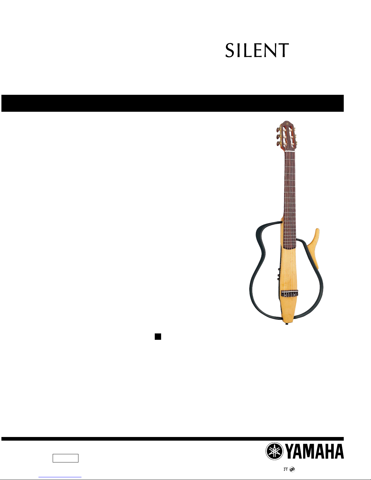
SPECIFICATIONS
Neck Mahogany
Body Maple
Fingerboard Rosewood
Bridge Rosewood
Frame Unit Maple
Strings Nylon Guitar Strings
Sensors B-BAND
Connectors/Controls • AUX IN
• AUX IN Level Control
• LINE OUT jack (monaural)
• PHONES jack (stereo)
• Volume
• BASS control
• TREBLE control
• REVERB switch (OFF/1/2)
• PHONES switch (ON/OFF)
• LINE OUT Jack with POWER Switch (Inserting a plug into the jack switches the
power on)
Power Supply • AC Adaptor/6F22 (S-006P) battery x1 dual
power source
* Recommended AC Adaptors: PA-D09, PA-
1E, PA-3B
Battery Life Continuous Use
• Using Manganese battery :
approximately 13.5 hours
• Using Alkaline battery :
approximately 24 hours
With the reverb activated
• Using Manganese battery :
approximately 2 hours
• Using Alkaline battery :
approximately 7.5 hours
Input/Output Specifications
Input Level
• AUX IN: -40 dBm/1kHz sine wave
(REVERB OFF)
Output Level
• LINE OUT: -27 dBm/10k Ω
• PHONES (L/R): -31 dBm/39 Ω
Power Consumption Using AC adaptor (PA-D09)
• REVERB OFF: 1.9 W
1- 2: 2.4 W
Using battery
• REVERB OFF: 0.2 W
1- 2 : 0.6 W
String Length 650 mm (25-9/16”)
Dimensions 965 (L) x 365 (W) x 80 (H) mm
38” (L) x 14-3/8” (W) x 3-1/8” (H)
(with the left frame attached and to the end
of the strap pin)
Weight approximately 1.8 kg (3 lbs. 15 oz.)
Accessories AC adaptor (PA-D09),
* May not be in your area.
Stereo earphones, Soft case
Page 4
SLG-100N
4
THIS DEVICE COMPLIES WITH PART 15 OF THE FCC
RULES. OPERATION IS SUBJECT TO THE FOLLOWING
TWO CONDEITIONS: (1) THIS DEVICE MAY NOT CAUSE
HARMFUL INTERFERENCE, AND (2) THIS DEVICE MUST
ACCEPT ANY INTERFERENCE RECEIVED, INCLUDING
INTERFERENCE THAT MAY CAUSE UNDESIRED
OPERATION.
¥ THIS CLASS B DIGITAL APPARATUS COMPLIES WITH
CANADIAN ICES-003.
¥ CET APPAREIL NUMÉRIQUE DE LA CLASSE B EST
CONFORME ¸ LA NORME NMB-003 DU CANADA.
AC POWER ADAPTOR :
YAMAHA PA-1E OR PA-3B OR PA-D09
BATTERY : 9V 6LR61 OR 6F22YBATTERY : 9V 6LR61 OR 6F22Y
MADE IN TAIWAN
SILENT GUITAR
MODEL SLG-100N
OPEN
LINE OUT
AUX IN
AUX VOL
MIN MAX
V
E
R
I
F
I
E
D
S
E
M
K
O
EMC
N89
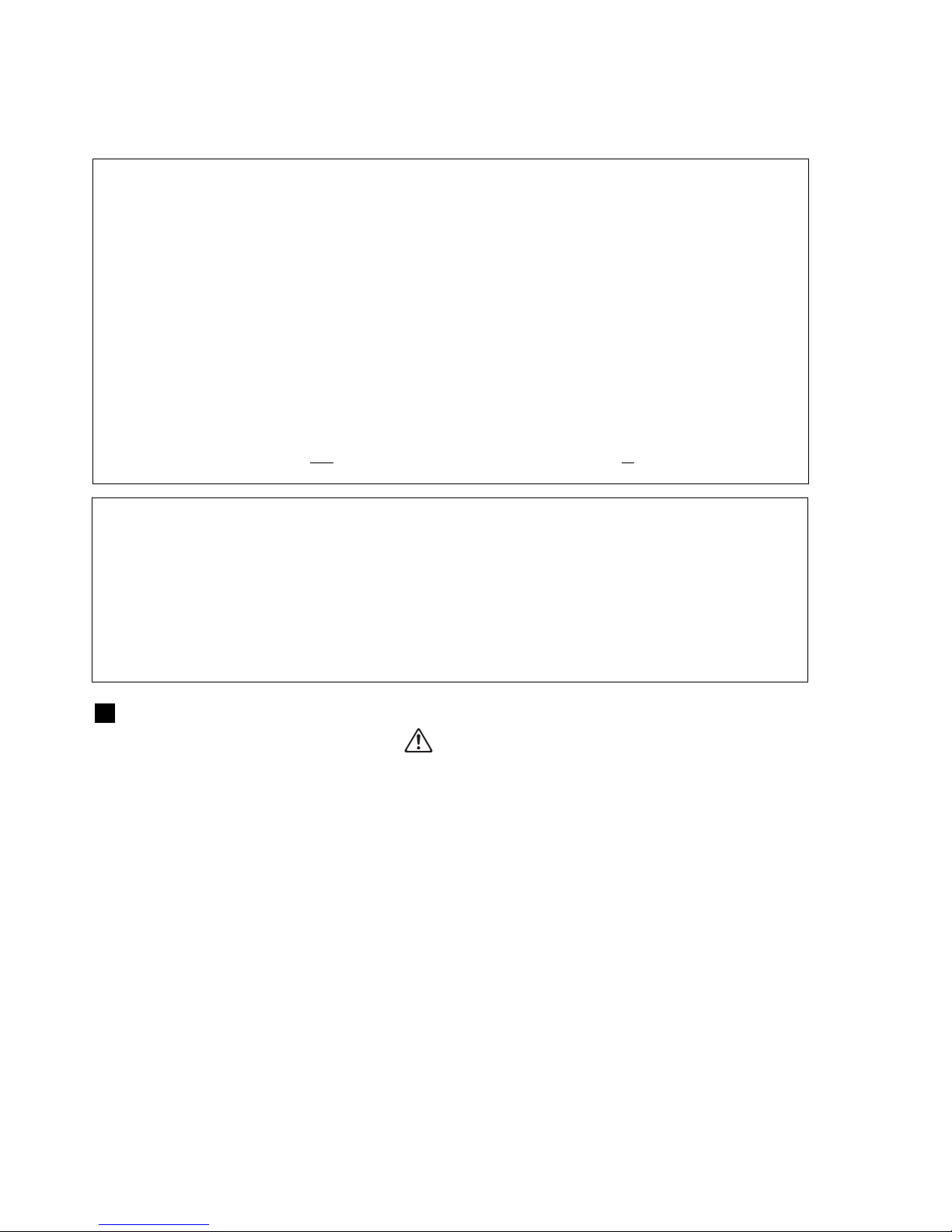
Front
Rear
Neck
Saddle
Tuning peg
Body
Pickup (underneath the saddle)
Controls → See page 5.
Frame Attachment Screw 1 (Doubles as the Strap Pin)
Left Frame (Removable)
Right Frame (Fixed)
Bridge
Horn (Leg Support)
Frame Attachment Screw 2 (Doubles as the Strap Pin)
Nut
Fingerboard
PANEL LAYOUT
Page 5
SLG-100N
5
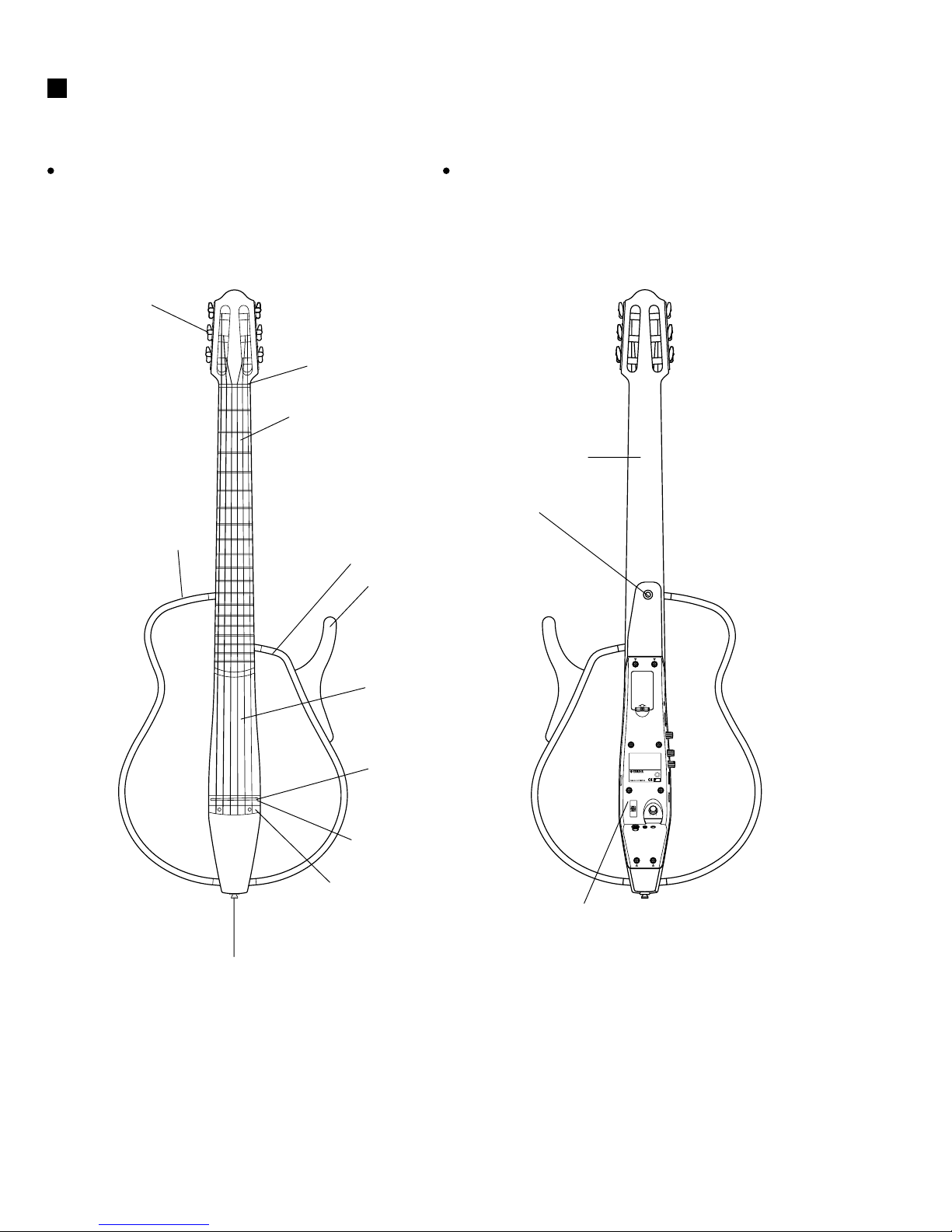
Controls
OFF 1 2 OFF ON
PHONES
REVERB VOLUME BASS TREBLE
THIS DEVICE COMPLIES WITH PART 15 OF THE FCC
RULES. OPERATION IS SUBJECT T O THE FOLLOWING
TWO CONDEITIONS: (1) THIS DEVICE MAY NOT CAUSE
HARMFUL INTERFERENCE, AND (2) THIS DEVICE MUST
ACCEPT ANY INTERFERENCE RECEIVED, INCLUDING
INTERFERENCE THAT MAY CAUSE UNDESIRED
OPERATION.
¥ THIS CLASS B DIGITAL APPARATUS COMPLIES WITH
CANADIAN ICES-003.
¥ CET APPAREIL NUMÉRIQUE DE LA CLASSE B EST
CONFORME ¸ LA NORME NMB-003 DU CANADA.
AC POWER ADAPTOR :
YAMAHA PA-1E OR PA-3B OR PA-D09
BATTERY : 9V 6LR61 OR 6F22YBATTERY : 9V 6LR61 OR 6F22Y
MADE IN TAIWAN
SILENT GUITAR
MODEL SLG-100N
OPEN
LINE OUT
AUX IN
AUX VOL
MIN MAX
V
E
R
I
F
I
E
D
S
E
M
K
O
EMC
N89
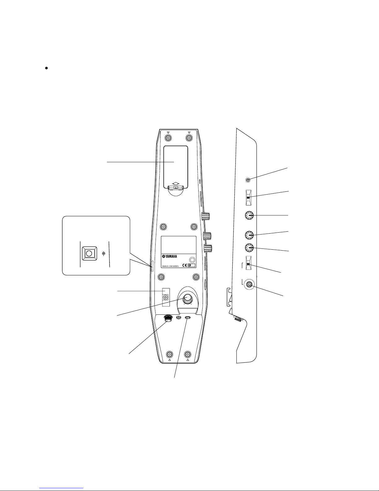
VOLUME control
6F22 (S-006P) 9V battery
REVERB switch
POWER lamp
AUX IN jack
AUX IN level control
Cord hook
LINE OUT jack
DC-IN jack
(Power adaptor connector)
BASS control
TREBLE control
PHONES ON/OFF switch
PHONES jack
DC-IN 9~12V
+–
Page 6
SLG-100N
6
CIRCUIT BOARD LAYOUT
MA
AUX
PUP
Jack
Panel Assembly
Body (rear view)
(underneath the panel assembly)
Page 7
SLG-100N
7
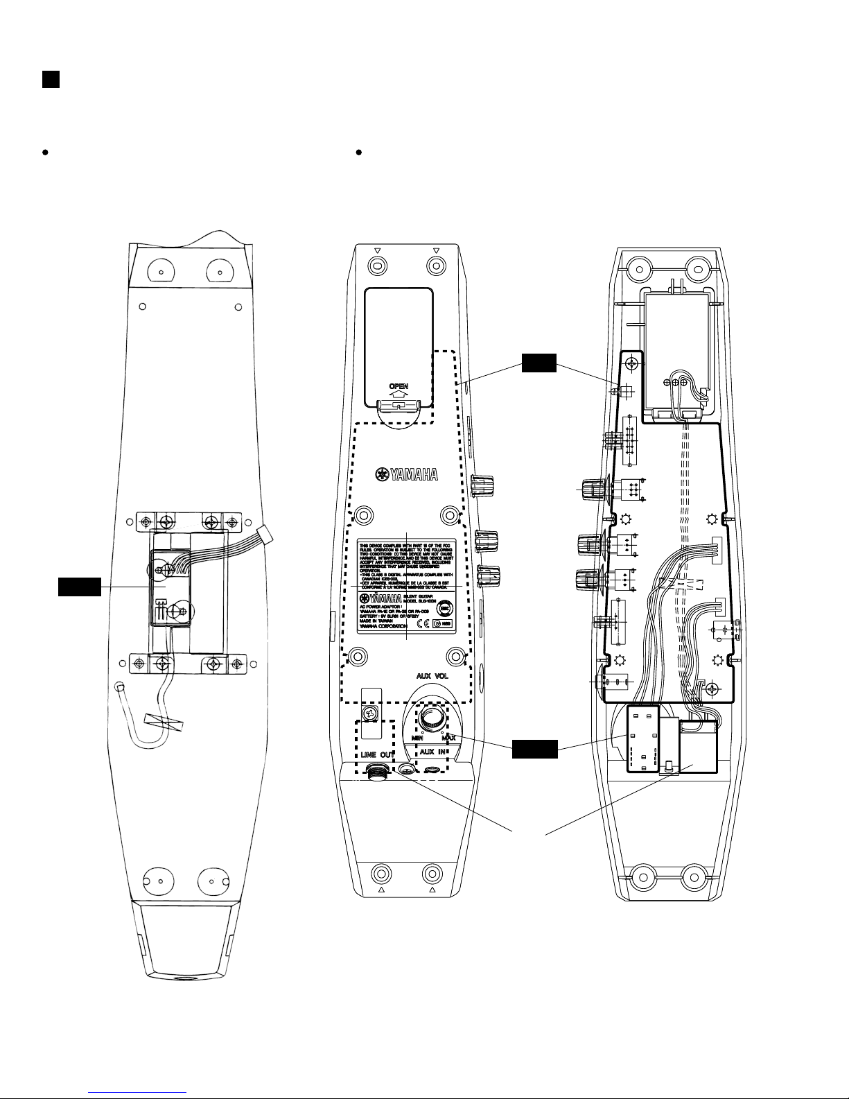
DISASSEMBLY PROCEDURE
Preparations
Make the following preparations;
Turn off the power switch.
Remove the battery cover and battery.
1. Left Frame (Time required: About 2 minutes)
1-1 Loosen the adjusting bolt (front) marked [E15] and the adjusting
bolt (rear) marked [E16]. The left frame can then be removed.
(Fig.1)
2. Bracket Assembly, Bracket, Sleeve
(Time required: About 5 minutes each)
2-1 Remove the left frame. (See procedure 1.)
2-2 Bracket Assembly:
Remove the two (2) screws marked [D05]. The upper bracket
assembly can then be removed from the left frame. (Fig.1)
The lower bracket assembly can be removed in the same manner.
2-3 Bracket, Sleeve:
Remove the two (2) screws marked [E19]. The upper bracket
and the upper sleeve can then be removed. (Fig.1)
The lower bracket and the lower sleeve can be removed in the
same manner.
3. Right Frame
(Time required: About 2 minutes)
3-1 Remove the four (4) screws marked [E22]. The right frame can
then be removed with the horn. (Fig.1)
4. Horn, Right Bracket
(Time required: About 5 minutes each)
4-1 Remove the right frame. (See procedure 3.)
4-2 Horn:
Remove the two (2) screws marked [D08]. The horn can then be
removed. (Fig.1)
4-3 Right Bracket:
Remove the two (2) screws marked [E21]. The upper right
bracket can then be removed. (Fig.1)
The lower right bracket can be removed in the same manner.
Peg
Peg
String
Bracket assembly
Bracket assembly
Right bracket
Right frame
Pickup
Panel holder assembly
Panel holder
Spacer
Horn
Right bracket
Bracket
Bracket
Sleeve
Left frame
[E19]
[D05]
Sleeve
[E19]
[E16]
[D05]
[
E22
]
[E21]
[D08]
[E21]
[E22]
[F02] X 4
[E15]
PUP
[D05]: Flat Head Tapping Screw-2
3.0X8 (QC667000)
[D08]: Flat Head Tapping Screw
3.5X20 (QC667100)
[E15]: Adjusting Bolt, Front
M6.0XP1X25 (QC653400)
[E16]: Adjusting Bolt, Rear
M6.0XP1X12 (QC653500)
[E19]: Flat Head Tapping Screw
3.0X14 ZMC2BL (QC699200)
[E21]: Flat Head Tapping Screw
3.0X14 ZMC2BL (QC699200)
[E22]: Flat Head Tapping Screw-2
3.0X8 (QC667000)
[F02]: Bind Head Tapping Screw-1
3.0X10 ZMC2BL (20404200)
Fig.1
Page 8

SLG-100N
8
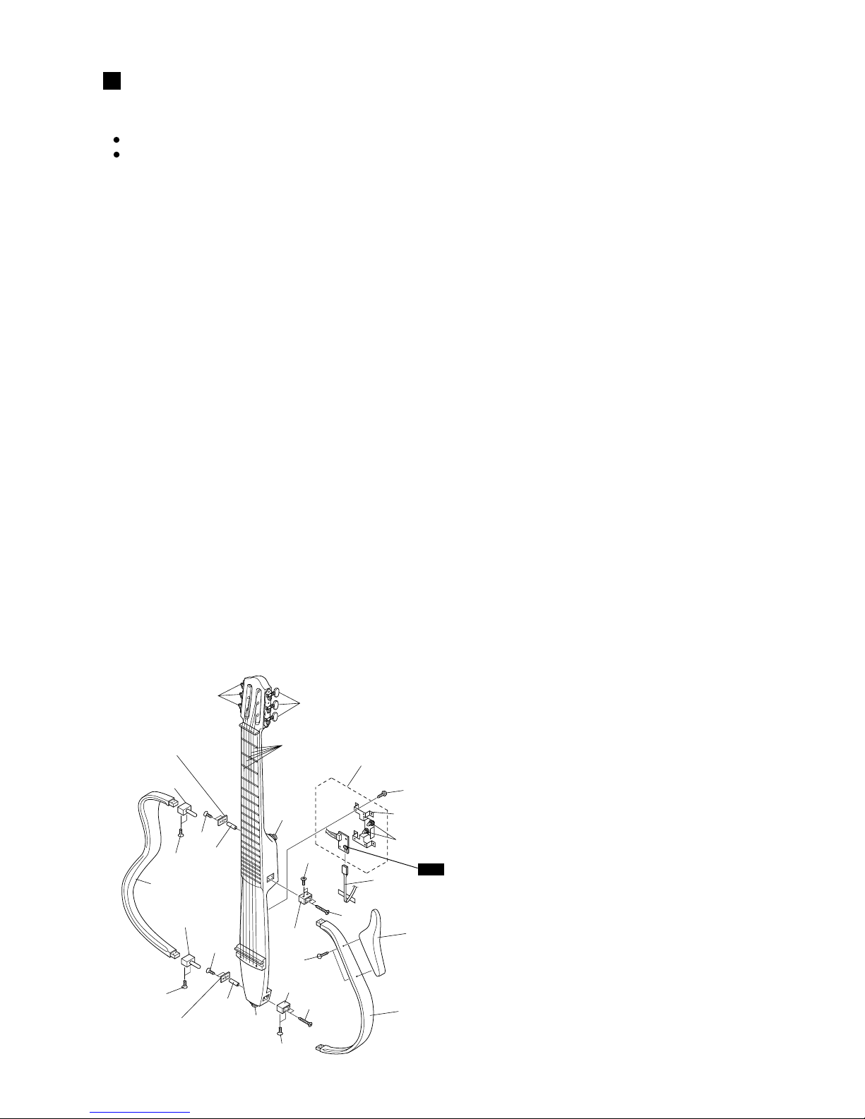
5. Peg (Time required: About 5 minutes)
5-1 Remove the three (3) strings in left side (4th-6th strings) and right
side (1
st-3rd
strings) each. (Fig.2)
5-2 Remove the four (4) screws marked [E03] in left and right each.
The left and right pegs can then be removed. (Fig.2)
Fig.2
[E03]
[E03]
Peg
Peg
Left side Strings (4
th-6th
)
Right side Strings (1
st-3rd
)
[E03]: Round Head Wood Screw 2.1X8 (03714060)
6. Panel Assembly (Time required: About 2 minutes)
6-1 Remove the four (4) screws marked [F05] and the four (4) screws
marked [F06]. The panel assembly can then be removed. (Fig.3)
7. MA Circuit Board, AUX Circuit Board,
Jack (LINE Connector Assembly)
(Time required: About 5 minutes each)
7-1 Remove the panel assembly. (See procedure 6.)
7-2 MA Circuit Board:
Pull out the three (3) rotary knobs for [VOLUME], [BASS] and
[TREBLE]. (Fig.3, 4)
Remove the two (2) screws marked [16A]. The MA circuit board
can then be removed. (Fig.4)
7-3 AUX Circuit Board:
Pull out the AUX knob and remove the screw marked [16B].
The AUX circuit board can then be removed with the jack holder .
(Fig.3, 4, 5)
Remove the hexagonal nut marked [A]. The jack holder can then
be removed from the AUX circuit board. (Fig.5)
7-4 Jack (LINE Connector Assembly):
Remove the hexagonal nut marked [10]. The jack (LINE
connector assembly) can then be removed. (Fig.3, 4)
Page 9

SLG-100N
9
[VOLUME]
[BASS]
[TREBLE]
[F05] [F06]
[16B]
[10]
Rotary knob
[F05]
Jack (LINE connector assembly)
AUX knob
Jack (LINE connector assembly)
Rotary knob
[VOLUME]
[BASS]
[TREBLE]
[16A]
[16A]
MA
AUX
Fig.4
[F05]: Bind Head Tapping Screw-1 3.0X10 ZMC2BL (20404200)
[F06]: Bind Head Tapping Screw-B 3.0X10 ZMC2BL (EP600140)
[10]: Hexagonal Nut (AA820860)
[16B]: Bind Head Tapping Screw-B 3.0X10 ZMC2BL (EP600140)
Fig.3
[16A]: Bind Head Tapping Screw-B 3.0X10 ZMC2BL (EP600140)
Fig.5
[A]: Hexagonal Nut
Photo.1
Bridge saddle
Bridge
PickupPickup
String
[A]
Jack holder
AUX
8. PUP Circuit Board (Time required: About 5 minutes)
8-1 Remove the panel assembly. (See procedure 6.)
8-2 Remove the four (4) screws marked [F02]. The panel holder
assembly can then be removed. (Fig.1)
8-3 Remove the PUP circuit board from the two (2) spacers. (Fig.1)
9. Pickup
(Time required: About 5 minutes)
9-1 Remove the panel assembly. (See procedure 6.)
9-2 Turn each pegs and loosen the strings. (Fig.1, Photo.1)
9-3 Remove the bridge saddle. (Photo.1)
9-4 Remove the pickup from the slot on the bridge. (Photo.1)
9-5 Disconnect the connector from the PUP circuit board. (Fig.1)
Page 10

SLG-100N
10
LSI PIN DESCRIPTION
1 MD4 I/O 33 AVDD - DC A+5Vs bus
2 MD3 I/O 34 VDD - DC D+5V
3 MD0 I/O External RAM interface data 35 TST0 - DC D+5V
4 MD1 I/O 36 TST1 - DC D+5V
5 MD2 I/O 37 DOEN - DC D+5V
6 MCKO O Master clock output 38 SDO1 O N.C.
7 XO O Crystal oscillator connection 39 SDO0 O N.C.
8 XI I Crystal oscillator connection 40 WC O N.C.
9 ER0 I 41 BCO O N.C
10 ER1 I Eary refrection preset select 42 MA0 O
11 ER2 I 43 MA1 O
12 REV0 I 44 MA2 O
13 REV1 I Effect select 45 MA3 O
14 REV2 I 46 MA4 O
15 MUTEN I DC D+5V 47 MA5 O External RAM interface address
16 ICN I Initial clear 48 MA6 O
17 PRG I DC D+5V 49 MA7 O
18 MODE I Preset mode (H=DC +5V) 50 MA12 O
19 VSS - Ground 51 MA14 O
20 AVSS - Ground 52 VSS - Ground
21 CVA - N.C. 53 MA10 O
22 AORL O N.C. 54 MA011 O
23 AORR O N.C. 55 MA09 O External RAM interface address
24 CHL I Sample hold capacitor connection 56 MA8 O
25 AIL I Lch ADC input 57 MA13 O
26 VDD - DC D+5V 58 VDD - DC D+5V
27 AIR I Rch ADC input 59 WEN I Write enable
28 CHR I Sample hold capacitor connection 60 OEN I Output enable
29 AOFL O Lch DAC output 61 CEN I Chip select
30 AOFR O Rch DAC output 62 MD7 I/O
31 AVDD - DC A+5V 63 MD6 I/O External RAM interface data
32 CVB I Rch midpoint voltage 64 MD5 I/O
PIN
NAME I/O FUNCTION
NO.
PIN
NAME I/O FUNCTION
NO.
YSS234
MA: IC01
DSP
(XN299A00) (Digital Sound Processor)
IC BLOCK DIAGRAM
NJM3404AM (XM527A00)
Dual Operational Amplifier
MA: IC08-13
PUP: IC15
NJM3414AM (XR294A00)
Dual Operational Amplifier
MA: IC14
1
2
3
4-V
8
7
6
5
Output A
+V
Non-Inverting
Input A
-DC Voltage Supply
+DC Voltage
Supply
Output B
Inverting
Input B
Non-Inverting
Input B
Inverting
Input A
+-
+-
1
2
3
4-V
8
7
6
5
Output A
+V
Non-Inverting
Input A
Ground
+DC Voltage
Supply
Output B
Inverting
Input B
Non-Inverting
Input B
Inverting
Input A
+-
+-
Page 11

SLG-100N
11
CIRCUIT BOARDS
REVERB
OFF/1/2
VOLUME
POWER Lamp
BASS TREBLE
ON/OFF
to Battery
terminal
to LINE OUT
Jack
DC-IN 9~12V
GR
AUX IN
AUX VOL
MIN/MAX
PHONES
to Pickup (B-BAND
)
MA Circuit Board
PUP Circuit Board
AUX Circuit Board
Component side Pattern side
Component side
Pattern side
Component side
Pattern side
Note: See parts list for details of circuit board component parts.
ENA-V872950-1, 2 0
Page 12

SLG-100N
12
INSPECTIONS
1. Required Equipment
High-sensitivity AC voltmeter (level meter)
Battery (006P) or power adapter (PA-D09)
2. Noise Level Measurement
Load resistance
[PHONES] jack: 39Ω (right and left each)
[LINE OUT] jack:10kΩ
(1) Turn on the power to the main unit, turn on the [PHONES]
switch, and check that the power LED (green) lights up.
(2) Connect the level meter to the [PHONES] jack.
(3) Turn the [VOLUME], [BASS] and [TREBLE] control dials to
the right most position (MAX).
(4) Stop the strings vibrating, measure the noise level, and check
that the noise levels for both right and left channels are –60dBm
or less.
(5) Disconnect the level meter from the [PHONES] jack and connect
it to the [LINE OUT] jack instead.
(6) Stop the strings vibrating, measure the noise level, and check
that the noise level is –60dBm or less.
3. Reverberation Inspection
(1) Connect a headphone to the [PHONES] jack.
(2) Pluck a string, switch the [REVERB] switch from “OFF” to “1”
and then to “2”, and check that the following effect is present at
both right and left headphone outputs.
REVERB Mode (reverberating time)
1 HALL (1.0 sec)
2 HALL (3.0 sec)
(3) Turn the [VOLUME] control dial to the left most position (MIN).
(4) Disconnect the headphone from the [PHONES] jack.
Page 13

SLG-100N
13
Use a tuning meter, pitch pipe, tuning fork, piano, etc.,
and to the open strings to the pitches shown below.
• If the string’s pitch is high, loosen the string until the string’s
pitch is slightly lower than the tuning pitch, then tune while
raising the string’s pitch.
Play the standard pitch “lah” (A3: 440Hz) on a tuning fork,
etc., and tune the open 5th string to the same pitch.
Play the pitch produced by pressing the 5th string at the 5th
fret, and tune the open 4th string to the same pitch.
Play the pitch produced by pressing the 4th string at the 5th
fret, and tune the open 3rd string to the same pitch.
Play the pitch produced by pressing the 3rd string at the 4th
fret, and tune the open 2nd string to the same pitch.
Play the pitch produced by pressing the 2nd string at the 5th
fret, and tune the open 1st string to the same pitch.
Play the pitch produced by pressing the 6th string at the 5th
fret, and tune the pitch at the 5th fret of the 6th string to the pitch
produced by the open 5th string.
Open 1stString's Pitch: E
Open 2
nd
String's Pitch: B
Open 3
rd
String's Pitch: G
Open 4
th
String's Pitch: D
Open 5
th
String's Pitch: A
Open 6
th
String's Pitch: E
1F 2F 3F 4F 5F
Open 1stString's Pitch: E
Open 2
nd
String's Pitch: B
Open 3
rd
String's Pitch: G
Open 4
th
String's Pitch: D
Open 5
th
String's Pitch: A
Open 6
th
String's Pitch: E
TUNING
Page 14

SLG-100N
14
PUP
AUX
MA
CN5
RE-H022SD-1190
OP AMP
SYSTEM RESET
SYSTEM RESET
DSP
SRAM 256K
OP AMP
OP AMP
22K
22K
22K
22K
VOLUME
PHONES
AUX VOL
DC-IN 9~12V
REVERB OFF/1/2
OP AMP
OP AMP
REGULATOR +8V
REGULATOR +5V
SYSTEM RESET
OP AMP
OP AMP
OP AMP
3.3K
1K1K
0.012u
TREBLE
BASS
TONE CONTROL
Note
Note: D7 is not installed.
to Pickup (B-BAND)
NJM78L08UA(XN00A00)
REGULATOR +8V
1: OUTPUT
2: COMMON
3: INPUT
1
2
3
NJU7202U50(X0150A00)
REGULATOR +5V
1: COMMON
2: INPUT
3: OUTPUT
1
2
3
: Mylar Capacitor
Note : See parts list for details of circuit board component parts.
STE-GA00P-04
2
LINE OUT
AUX IN
BATTERY
(+9V)
Power Lamp
GR
TO SERVICE PERSONNEL
Critical Components Information
Components having special characteristics are marked
and must be replaced with parts having specifications
equal to those originally installed.
+–
OVERALL CIRCUIT DIAGRAM
Page 15

PARTS LIST
WARNING
Components having special characteristics are marked and must be replaced with parts having
specification equal to those originally installed.
Notes : DESTINATION ABBREVIATIONS
The numbers “QTY” show quantities for each unit.
The parts with “--” in “PART NO.” are not available as spare parts.
This mark “ } ” in the REMARKS column means these parts are interchangeable.
The second letter of the shaded (
) part number is O, not zero.
The second letter of the shaded (
) part number is I, not one.
M: South African model
O: Chinese model
Q: South-east Asia model
T : Taiwan model
U : U.S.A. model
V : General export model (110V)
W: General export model (220V)
N,X: General export model
Y : Export model
A : Australian model
B : British model
C : Canadian model
D : German model
E : European model
F : French model
H : North European model
I : Indonesian model
J : Japanese model
CONTENTS
OVERALL ASSEMBLY .............................................. 2
PANEL ASSEMBLY ......................................... 4
ELECTRICAL PARTS ............................................. 6
SLG-100N
Guitar
Page 16

SLG-100N
2
OVERALL ASSEMBLY
F05
F06
F04
F02
F03
F09
F07
F08
E21
E21
E20
E20
E22
E16
E22
E15
A01
D07
D06
D08
E05
E08
E06
E07
D02
D01
E03
E03
E01
E04
E01
D05
D05
D04
D04
E14
E13
E12
E11
E10 E09
D03
E19
E17
E18
E19
E17
E18
F01
F01a
F01b
F01e
F01c
F01d
F01d
Panel assembly: See page 4.
Panel holder assembly
Page 17

SLG-100N
3
REF NO.
PART NO. DESCRIPTION REMARKS
QTY
: New Parts RANK: Japan only
*
*
*
*
*
*
*
*
*
*
*
*
*
*
*
*
*
*
*
*
*
*
*
*
*
*
*
*
*
*
*
OVERALL ASSEMBLY SLG-100N
A01 Body
D01 Nut S M6.0XP1 L=13 #0186130
D02 Nut S M6.0XP1 L=10 #0186100
D03 Left Frame
D04 Bracket Assembly 2
D05 Flat Head Tapping Screw-2 3.0X8(Black Chrome) 4
D06 Right Frame
D07 Horn Maple
D08 Flat Head Tapping Screw 3.5X20(Black Chrom) 2
E01 Tuning Machine Assembly Pingway RM-1388 (Gold) 1set
E03 Round Head Wood Screw 2.1X8 (Brass) 801
E04 Nut Urea 50mm (White)
E05 Bridge Indian Rosewood
E06 Oval Head Wood Screw 2.4X16 (Chrome) 201
E07 Cap M5.0 (White) 201
E08 Bridge Saddle Urea 82mm (White)
E09 String 1 CG S11 (QA33300)
E10 String 2 CG S12 (QA33310)
E11 String 3 CG S13 (QA33320)
E12 String 4 CG S14 (QA25310)
E13 String 5 CG S15 (QA25320)
E14 String 6 CG S16 (QA25330)
E15 Adjusting Bolt, Front M6.0XP1X25 (Black)
E16 Adjusting Bolt, Rear M6.0XP1X12 (Black)
E17 Bracket (Black) 2
E18 Sleeve (Blue) 2
E19 Flat Head Tapping Screw 3.0X14 ZMC2BL (Black) 4
E20 Right Bracket (Black) 2
E21 Flat Head Tapping Screw 3.0X14 ZMC2BL (Black) 4
E22 Flat Head Tapping Screw-2 3.0X8(Black Chrome) 4
F01 Panel Holder Assembly (QC66260)
F01a Panel Holder
F01b Circuit Board PUP
F01c Spacer ACBS-2 (PINGOOD) 2
F01d Sponge 8X8 t=7 (QC68960) 2
F01e Connector Assembly PUP PHR-5P L=70 (QC66180)
F02 Bind Head Tapping Screw-1 3.0X10 ZMC2BL (Black) 4
F03 Aluminum Sheet (QC66250)
F04 Panel Assembly (QC66720)
F05 Bind Head Tapping Screw-1 3.0X10 ZMC2BL (Black) 4
F06 Bind Head Tapping Screw-B 3.0X10 ZMC2BL (Black) 4 01
F07 Pickup B-Band 29S
F08 Adhesive T ape 12X50 t=0.2 (QC66730)
F09 Cushion 8X12 t=1
ACCESSORIES
H01 AC Adapter PA-D09 J J
H01 AC Adapter PA-D09 UL U,C
H01 AC Adapter PA-D09 CE H
H02 Stereo Earphones
H03 Soft Case
--
24173400
QC665900
QC653700
QC655100
QC667000
QC653600
QC655400
QC667100
QC666400
03714060
QC656400
QC655200
20454100
03377460
QC656500
--
--
--
--
--
-QC653400
QC653500
QC693600
QC653300
QC699200
QC653100
QC699200
QC667000
-QC660000
V8729900
QC662400
--
-20404200
--
-20404200
EP600140
QC624400
-QC679000
V8285200
V8285300
V8285400
QC667400
QC666900
RANK
Accessories
H01
AC Adapter
H02
Stereo Earphones
H03
Soft Case
Page 18

SLG-100N
4
PANEL ASSEMBLY
16
16
6
4
2
1
15
3
16
18
5
11
10
18
16
9a
9
8
7
19
17
13
12
14
Page 19

SLG-100N
5
REF NO.
PAR T NO. DESCRIPTION REMARKS
QTY
: New Parts RANK: Japan only
*
*
*
*
*
*
*
*
PANEL ASSEMBLY SLG-100N (QC66720)
1 Control Panel (Black)
2 Battery Cover (Black)
3 AUX Knob AUX V OL 04
4 Rotary Knob VOLUME,BASS,TREBLE 3 05
5 DC Cord Column 02
6 Circuit Board MA
7 Circuit Board AUX
8 Jack Holder
9 Connector Assembly LINE PHR-3P (QC66160)
9a Jack JL2B X-G7639 LINE OUT 03
10 Hexagonal Nut (Black) 01
11 Flat Washer (Black) 01
12 Connector Assembly BT PHR-2P L=280 with Battery snap
13 Sponge 20X37 t=4 (Gray) (QC66190) 2
14 Adhesive Tape 5X20 t=0.2 (QC66730)
15 Name Plate Sticker (QC66230)
16 Bind Head Tapping Screw-B 3.0X10 ZMC2BL (Black) 4 01
17 Cushion 8X12 t=1
18 Flat Washer 3.0X8X0.5 ZMC2BL (Black) 2
19 Cushion 20X20X13 (Black) (QC70870)
-QC659900
QC660200
V2300100
QC187700
VC407100
V8729700
V8729800
QC660100
-LB201120
AA820860
AA820850
QC661500
--
--
-EP600140
QC679000
QC689700
--
RANK
Page 20

SLG-100N
6
REF NO.
PART NO. DESCRIPTION REMARKS
QTY
: New Parts RANK: Japan only
*
*
*
*
*
*
*
ELECTRICAL PARTS SLG-100N
Circuit Board MA (V872950)(X2450C0)
Circuit Board AUX (V872950)(X2450C0)
Circuit Board PUP (V872950)(X2450C0)
Circuit Board MA (V872950)(X2450C0)
LED Holder LEH5-4.5T
C01 Mylar Capacitor 0.047u 50V J 01
C02 Mylar Capacitor 0.012u 50V J 01
C03 Ceramic Capacitor-F (chip) 0.1u 25V Z 01
C04 Ceramic Capacitor-SL(chip) 150P 50V J 01
C05 Mylar Capacitor 0.018u 50V J 01
C06 Mylar Capacitor 0.01u 50V J 01
C07 Ceramic Capacitor-B (chip) 3300P 50V K 01
C08 Ceramic Capacitor-F (chip) 0.1u 25V Z 01
C09 Mylar Capacitor 2200P 50V J 01
C10 Mylar Capacitor 560P 50V J 02
C11 Mylar Capacitor 0.068u 50V J 02
C12 Ceramic Capacitor-CH(chip) 22P 50V J 01
C13 Ceramic Capacitor-CH(chip) 22P 50V J 01
C14 Ceramic Capacitor-SL(chip) 100P 50V J 01
C15 Mylar Capacitor 0.01u 50V J 01
C16 Mylar Capacitor 0.022u 50V J 01
C17 Mylar Capacitor 0.022u 50V J 01
C18 Ceramic Capacitor-F (chip) 0.1u 25V Z 01
C19 Ceramic Capacitor-B (chip) 3300P 50V K 01
C20 Mylar Capacitor 0.022u 50V J 01
C21 Ceramic Capacitor-F (chip) 0.1u 25V Z 01
C22 Mylar Capacitor 0.022u 50V J 01
C23 Ceramic Capacitor-B (chip) 3300P 50V K 01
C24 Ceramic Capacitor-F (chip) 0.1u 25V Z 01
C25 Ceramic Capacitor-F (chip) 0.1u 25V Z 01
C26 Ceramic Capacitor-SL(chip) 100P 50V J 01
C27 Ceramic Capacitor-SL(chip) 100P 50V J 01
C28 Mylar Capacitor 0.047u 50V J 01
C29 Mylar Capacitor 0.047u 50V J 01
C30 Ceramic Capacitor-F (chip) 0.1u 25V Z 01
C31 Mylar Capacitor 0.01u 50V J 01
C32 Mylar Capacitor 0.01u 50V J 01
C33 Ceramic Capacitor-F (chip) 0.1u 25V Z 01
C34 Ceramic Capacitor-F (chip) 0.1u 25V Z 01
C35 Mylar Capacitor 0.022u 50V J 01
C36 Mylar Capacitor 0.022u 50V J 01
C37 Ceramic Capacitor-F (chip) 0.1u 25V Z 01
C38 Ceramic Capacitor-B (chip) 1500P 50V K 01
C39 Ceramic Capacitor-B (chip) 1500P 50V K 01
C40 Ceramic Capacitor-F (chip) 0.1u 25V Z 01
C41 Mylar Capacitor 0.068u 50V J 02
C42 Mylar Capacitor 0.068u 50V J 02
C43 Ceramic Capacitor-F (chip) 0.1u 25V Z 01
C44 Ceramic Capacitor-B (chip) 4700P 50V K 01
C45 Ceramic Capacitor-F (chip) 0.1u 25V Z 01
C46 Ceramic Capacitor-SL(chip) 330P 50V J 01
C47 Ceramic Capacitor-F (chip) 0.1u 25V Z 01
C48 Ceramic Capacitor-SL(chip) 150P 50V J 01
-51 Ceramic Capacitor-SL(chip) 150P 50V J 01
C52 Ceramic Capacitor-F (chip) 0.1u 25V Z 01
-55 Ceramic Capacitor-F (chip) 0.1u 25V Z 01
CC01 Electrolytic Capacitor-KS 100u 6.3V 01
-03 Electrolytic Capacitor-KS 100u 6.3V 01
CC04 Electrolytic Capacitor-KS 220u 10V
CC05 Electrolytic Capacitor-KS 220u 10V
CC06 Electrolytic Capacitor-BP 0.47u 50V 01
CC07 Electrolytic Capacitor-KS 100u 16V 01
CC08 Electrolytic Capacitor-KS 10u 16V 01
CC09 Electrolytic Capacitor-KS 100u 16V 01
CC10 Electrolytic Capacitor-KS 4.7u 25V 01
CC11 Electrolytic Capacitor-KS 1u 50V 01
CC12 Electrolytic Capacitor-KS 1u 50V 01
CC13 Electrolytic Capacitor-KS 47u 16V 01
V8729700
V8729800
V8729900
V8729700
QC662200
UA654470
UA354120
US145100
US062150
UA654180
UA654100
US063330
US145100
UA653220
UA652560
UA654680
US061220
US061220
US062100
UA654100
UA654220
UA654220
US145100
US063330
UA654220
US145100
UA654220
US063330
US145100
US145100
US062100
US062100
UA654470
UA654470
US145100
UA654100
UA654100
US145100
US145100
UA654220
UA654220
US145100
US063150
US063150
US145100
UA654680
UA654680
US145100
US063470
US145100
US062330
US145100
US062150
US062150
US145100
US145100
UM388100
UM388100
V6796100
V6796100
UN865470
UM398100
UM397100
UM398100
UM406470
UM416100
UM416100
UM397470
RANK
ELECTRICAL PARTS
Page 21

SLG-100N
7
REF NO.
PART NO. DESCRIPTION REMARKS
QTY
: New Parts RANK: Japan only
*
*
*
*
RANK
CC14 Electrolytic Capacitor-KS 47u 16V 01
CC15 Electrolytic Capacitor-FW 220u 25V
CC16 Electrolytic Capacitor-KS 220u 10V
CC17 Electrolytic Capacitor-KS 220u 10V
CC18 Electrolytic Capacitor-KS 100u 16V 01
CC19 Electrolytic Capacitor-KS 10u 16V 01
CN1 Connector Base Post 5P B5B-PH-K-S to PUP-CN6 01
CN2 Connector Base Post 2P B2B-PH-K-S to Battery 9V 01
CN3 Connector Base Post 3P B3B-PH-K-S to LINE OUT 01
CN4 Connector Base Post 4P B4B-PH-K-S to AUX-CN7 01
D01 Diode 1SR154-400 (1A) 01
D02 Diode 1SR154-400 (1A) 01
D03 Diode RB160L-40 01
-05 Diode RB160L-40 01
D06 Diode 1SS355 01
D08 Diode 1SS355 01
-13 Diode 1SS355 01
FT1 FET 2SK208-Y 01
-4 FET 2SK208-Y 01
IC01 IC YSS234 (SP3) DSP 11
IC02 IC UPD43256BGW-70LL-9 SRAM 256K
IC03 IC PST594C-MMP4P SYSTEM RESET 03
IC04 IC PST9242NR SYSTEM RESET 01
IC05 IC PST594E-MT SYSTEM RESET 03
IC06 IC NJU7202U50 REGULATOR +5V 03
IC07 IC NJM78L08UA REGULATOR +8V 01
IC08 IC NJM3404AM OP AMP 03
-13 IC NJM3404AM OP AMP 03
IC14 IC NJM3414AM OP AMP 02
JK1 Connector HEC0470-01-630 DC-IN 9-12V 02
JK2 ST Mini Jack JC-6 PHONES 01
LD1 LED Green GL3EG8 POWER lamp 01
R01 Carbon Resistor (chip) 2.7K 63M J 01
R02 Carbon Resistor (chip) 1.0K 63M J 01
R03 Carbon Resistor (chip) 3.3K 63M J 01
R04 Carbon Resistor (chip) 1.0K 63M J 01
R05 Carbon Resistor (chip) 6.8K 63M J 01
R06 Carbon Resistor (chip) 10K 63M J 01
R07 Carbon Resistor (chip) 1K 63M J 01
R08 Carbon Resistor (chip) 8.2K 63M J 01
R09 Carbon Resistor (chip) 470 63M J 01
R10 Carbon Resistor (chip) 1K 63M J 01
R11 Carbon Resistor (chip) 8.2K 63M J 01
R12 Carbon Resistor (chip) 470 63M J 01
R13 Carbon Resistor (chip) 100K 63M J 01
R14 Carbon Resistor (chip) 10K 63M J 01
R15 Carbon Resistor (chip) 1K 63M J 01
R16 Carbon Resistor (chip) 1.2K 63M J 01
R17 Carbon Resistor (chip) 100K 63M J 01
R18 Carbon Resistor (chip) 100K 63M J 01
R19 Carbon Resistor (chip) 10K 63M J 01
R20 Carbon Resistor (chip) 100K 63M J 01
R21 Carbon Resistor (chip) 2.2K 63M J 01
R22 Carbon Resistor (chip) 1M 63M J 01
R23 Carbon Resistor (chip) 4.7K 63M J 01
R24 Carbon Resistor (chip) 470 63M J 01
R25 Carbon Resistor (chip) 2.2K 63M J 01
R26 Carbon Resistor (chip) 27K 63M J 01
R27 Carbon Resistor (chip) 2.2K 63M J 01
R28 Carbon Resistor (chip) 0 63M J 01
R29 Carbon Resistor (chip) 47K 63M J 01
R30 Carbon Resistor (chip) 4.7K 63M J 01
R31 Carbon Resistor (chip) 4.7K 63M J 01
R32 Carbon Resistor (chip) 47K 63M J 01
R33 Carbon Resistor (chip) 10K 63M J 01
-36 Carbon Resistor (chip) 10K 63M J 01
R37 Carbon Resistor (chip) 100K 63M J 01
R38 Carbon Resistor (chip) 100K 63M J 01
R39 Carbon Resistor (chip) 2.2K 63M J 01
-44 Carbon Resistor (chip) 2.2K 63M J 01
UM397470
UU148220
V6796100
V6796100
UM398100
UM397100
VB390100
VB389800
VB389900
VB390000
VT532500
VT532500
VS597600
VS597600
VT332900
VT332900
VT332900
VR043100
VR043100
XN299A00
X2200A00
XT627A00
XZ000A00
XT657A00
X0150A00
XN000A00
XM527A00
XM527A00
XR294A00
LB302260
VJ573000
VR043700
RD356270
RD356100
RD356330
RD356100
RD356680
RD357100
RD356100
RD356820
RD355470
RD356100
RD356820
RD355470
RD358100
RD357100
RD356100
RD356120
RD358100
RD358100
RD357100
RD358100
RD356220
RD359100
RD356470
RD355470
RD356220
RD357270
RD356220
RD350000
RD357470
RD356470
RD356470
RD357470
RD357100
RD357100
RD358100
RD358100
RD356220
RD356220
Page 22

SLG-100N
8
REF NO.
PART NO. DESCRIPTION REMARKS
QTY
: New Parts RANK: Japan only
*
*
*
*
*
*
*
*
*
RANK
R45 Carbon Resistor (chip) 1M 63M J 01
R46 Carbon Resistor (chip) 2.2K 63M J 01
R47 Carbon Resistor (chip) 100K 63M J 01
-49 Carbon Resistor (chip) 100K 63M J 01
R50 Carbon Resistor (chip) 1K 63M J 01
R51 Carbon Resistor (chip) 22K 63M J 01
R52 Carbon Resistor (chip) 22K 63M J 01
R53 Carbon Resistor (chip) 3.3K 63M J 01
R54 Carbon Resistor (chip) 3.3K 63M J 01
R55 Carbon Resistor (chip) 18K 63M J 01
R56 Carbon Resistor (chip) 3.3K 63M J 01
R57 Carbon Resistor (chip) 3.3K 63M J 01
R58 Carbon Resistor (chip) 18K 63M J 01
R59 Carbon Resistor (chip) 22K 63M J 01
R60 Carbon Resistor (chip) 22K 63M J 01
R61 Carbon Resistor (chip) 10K 63M J 01
R62 Carbon Resistor (chip) 22K 63M J 01
-65 Carbon Resistor (chip) 22K 63M J 01
R66 Carbon Resistor (chip) 1K 63M J 01
R67 Carbon Resistor (chip) 10K 63M J 01
R68 Carbon Resistor (chip) 47 1/4W J 01
R69 Carbon Resistor (chip) 47 1/4W J 01
R70 Carbon Resistor (chip) 10K 63M J 01
R71 Carbon Resistor (chip) 10K 63M J 01
R72 Carbon Resistor (chip) 47 1/4W J 01
R73 Carbon Resistor (chip) 1K 63M J 01
R74 Carbon Resistor (chip) 100K 63M J 01
R81 Carbon Resistor (chip) 10K 63M J 01
SW1 Slide Switch SSSU124900 REVERB(OFF/1/2)
SW2 Slide Switch SSSU141800 PHONES(OFF/ON)
TR1 Transistor 2SC4081 01
VR1 Rotary Variable Resistor B10K RK09L1120 TREBLE
VR2 Rotary Variable Resistor B10K RK09L1120 BASS
VR3 Rotary Variable Resistor A10Kx2 RK09L12B0 VOLUME
X1 Quartz Crystal Unit 12.288MHz SMD-49 03
Circuit Board AUX (V872950)(X2450C0)
C61 Ceramic Capacitor-SL(chip) 100P 50V J 01
C62 Ceramic Capacitor-SL(chip) 100P 50V J 01
CN7 Connector Assembly AUX 4P L=100 to MA-CN4 (V875540)
JK4 Jack ST. HSJ0912-01-040 AUX IN
VR4 Rotary Variable Resistor A10Kx2 RK14K12D0A6 AUX V OL 03
Circuit Board PUP (V872950)(X2450C0)
C56 Mylar Capacitor 0.01u 50V J 01
C57 Mylar Capacitor 0.047u 50V J 01
C58 Ceramic Capacitor-SL(chip) 100P 50V J 01
C59 Ceramic Capacitor-SL(chip) 680P 50V J 01
C60 Ceramic Capacitor-F (chip) 0.1u 25V Z 01
CC20 Electrolytic Capacitor 10u 16V 01
CN5 Connector Base Post 2P MB2P-90H to Pickup (B-Band)
CN6 Connector Base Post 5P S5B-PH-K-S to MA-CN1 01
FT5 FET 2SK208-Y 01
IC15 IC NJM3404AM OP AMP 03
R75 Carbon Resistor (chip) 10K 63M J 01
R76 Carbon Resistor (chip) 4.7K 63M J 01
R77 Carbon Resistor (chip) 1K 63M J 01
R78 Carbon Resistor (chip) 100K 63M J 01
R79 Carbon Resistor (chip) 22K 63M J 01
R80 Carbon Resistor (chip) 22K 63M J 01
R82 Carbon Resistor (chip) 4.7M 63M J
R83 Carbon Resistor (chip) 4.7M 63M J
Jack JL2B X-G7639 LINE OUT 03
Pickup B-Band 29S
RD359100
RD356220
RD358100
RD358100
RD356100
RD357220
RD357220
RD356330
RD356330
RD357180
RD356330
RD356330
RD357180
RD357220
RD357220
RD357100
RD357220
RD357220
RD356100
RD357100
RD154470
RD154470
RD357100
RD357100
RD154470
RD356100
RD358100
RD357100
V8350200
V8190000
VQ986700
V8349900
V8349900
V8349800
VY891500
V8729800
US062100
US062100
-VC310700
V3175800
V8729900
UA654100
UA654470
US062100
US062680
US145100
UI337100
V9083500
VB858400
VR043100
XM527A00
RD357100
RD356470
RD356100
RD358100
RD357220
RD357220
RD359470
RD359470
LB201120
QC624400
 Loading...