Xysemi XR2201D Schematic [ru]

XR2201D
_____________________________ _________
1.2MHZ,14V Step-up DC/DC Converter
GENERAL DESCRIPTION
The XR2201D is a high frequency, high
efficiency DC to DC converter with an
integrated 4A, 0.1Ω power switch capable
of providing an output voltage up to 14V.
The fixed 1.2MHz allows the use of small
external inductions and capacitors and
provides fast transient response. It
integrates Soft start, Comp,. only need few
components outside.
FEATURES
z 2.3V to 6V input voltage Rangel
z Efficiency up to 96%
z 14V Boost converter with 4A switch
current
z 1.2Mhz fixed Switching Frequency
z Integrated soft-start
z Thermal Shutdown
z Under voltage Lockout
z ESD 8KV Pass( HBM )
z 8-Pin MSOP Package
APPLICATIONS
• Handheld Devices
• GPS Receiver
• Digital Still Camera
• Portable Applications
• DSL Modem
• PCMCIA Card
• TFT LCD Bias Supply
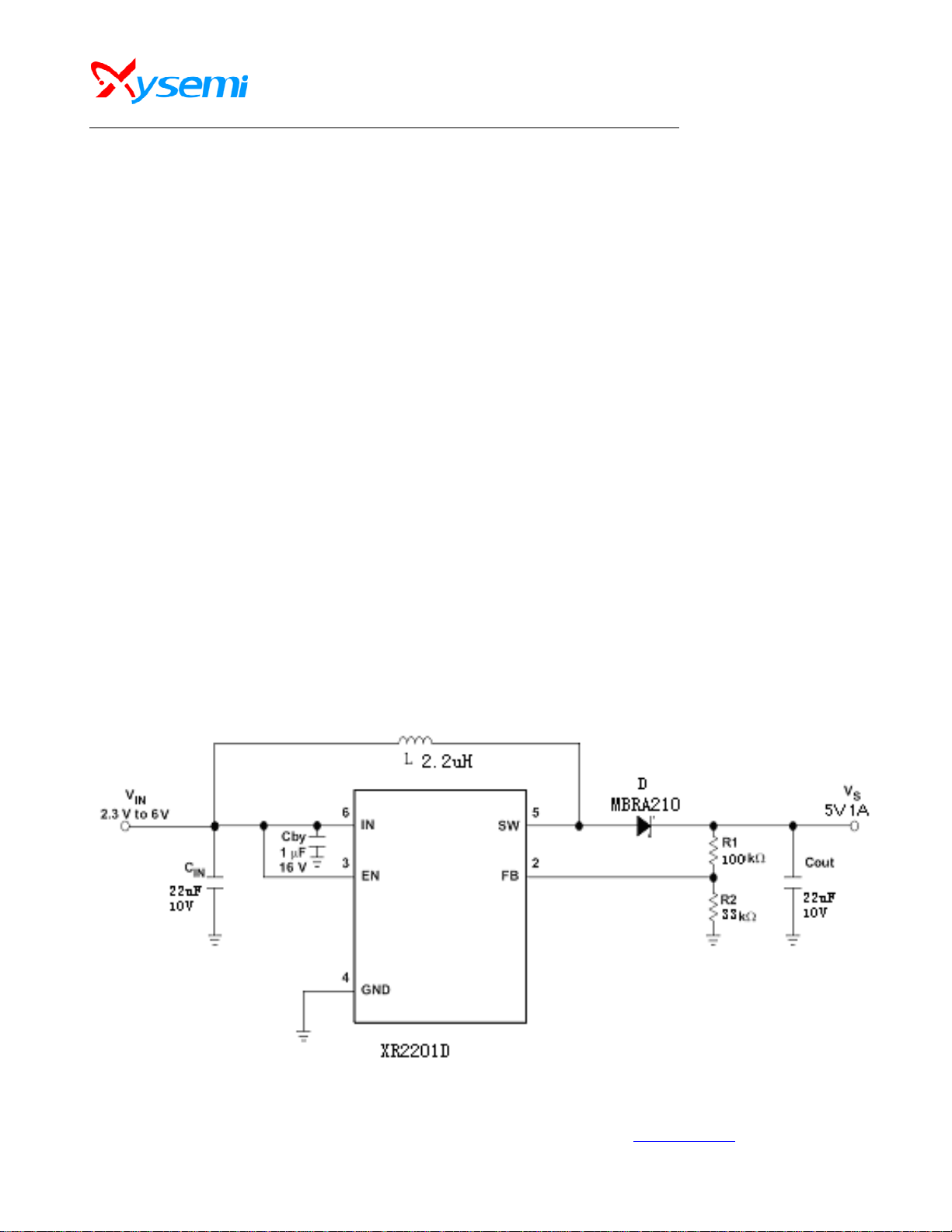
Figure 1. Typical Application Circuit1
XySemi Inc - 1 - www.xysemi.com
REV0.4

XR2201D
A
_____________________________ _________
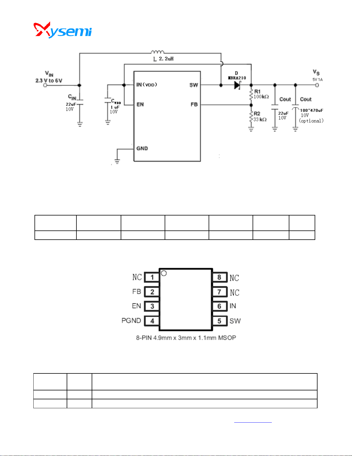
Figure 2. Typical Application Circuit2
ORDERING INFORMATION
PART
NUMBER
XR2201D -40°C to 85°C 1.2MHZ
TEMP RANGE
SWICHING
FREQUENCY
PIN CONFIGURATION
PIN DESCRIPTION
PIN
NUMBER
1 NC Not use
2 FB Feedback pin
PIN
NAME
OUTPUT
VOLTAGE (V)
DJ 4 MSOP 8
Figure 3. PIN Configuration
PIN DESCRIPTION
ILIM (A) PACKAGE PINS
XySemi Inc - 2 - www.xysemi.com
REV0.4

XR2201D
_________________________________________________________________________________________________
3 EN Shutdown control input., Connect this pin to logic high level to enable the device
4 PGND Power ground
5 SW Switch pin
6 IN Input power supply pin
7 NC Not use
8 NC Not use
ABSOLUTE MAXIMUM RATINGS
(Note: Do not exceed these limits to prevent damage to the device. Exposure to absolute maximum rating
conditions for long periods may affect device reliability.)
PARAMETER VALUE UNIT
Supply Voltage VIN -0.3 to 6.5 V
FB, EN Voltage -0.3 to VIN+0.3 V
SW Voltage Vin+0.3 to 15V V
Operating Ambient Temperature
Maximum Junction Temperature 150 °C
Storage Temperature -55 to 150 °C
Lead Temperature (Soldering, 10 sec) 300 °C
-40 to 85 °C
ELECTRICAL CHARACTERISTICS
(VIN = 3.6V, TA= 25°C unless otherwise specified)
PARAMETER SYMBOL TEST CONDITIONS MIN TYP MAX UNIT
Input Voltage Range V
Boost output voltage range Vout 14 V
Operating Supply Current
I
SUPPLY
Shutdown Supply Current
Regulated Feedback Voltage V
Peak Inductor Current I
Oscillator Frequency F
PEAK
OSC
Rds(ON) of N-channel FET ISW =-100mA 0.1 0.2 Ohm
Enable Threshold VIN = 2.3V to 5.5V 0.3 1 1.5 V
2.3 6.0 V
IN
=1.5V,EN=Vin, I
V
FB
Load
=0
75 135
µA
VEN =0V, VIN =4.2V 0.1 1
1.21 1.24 1.27 V
FB
4.0 A
0.9 1.2 1.5 MHz
XySemi Inc - 3 - www.xysemi.com
REV0.4

XR2201D
_________________________________________________________________________________________________
Enable Leakage Current -0.1 0.1 µA
SW Leakage Current
VEN = 0V, VSW = 0V or 5V, VIN = 5V
1 uA
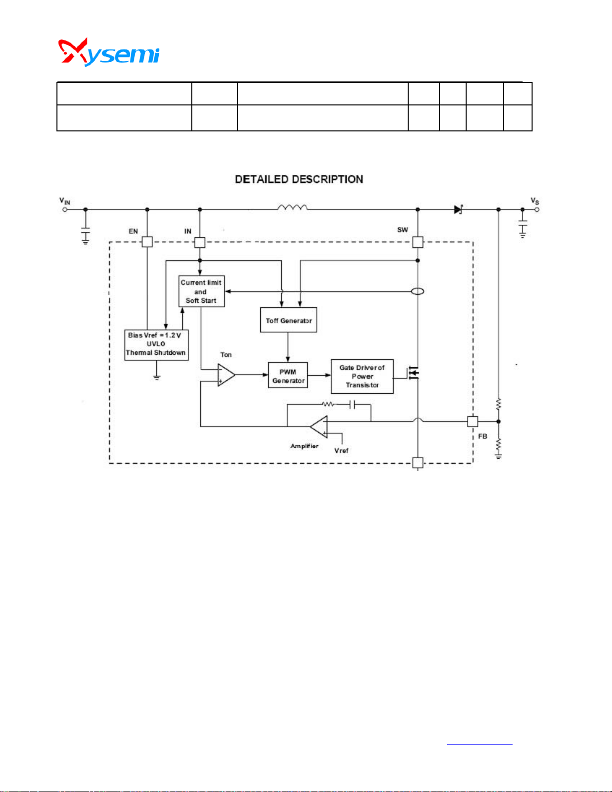
Figure 4. Functional Block Diagram
FUNCTIONAL DESCRIPTION
NORMAL OPERATION
The boost converter is designed for output
voltage up to 14V with a switch peak current limit of
4.0 A. The device, which operates in a current
mode scheme with quasi-constant frequency, is
externally 1.2MHZ and the minimum input voltage is
2.3 V. To control the inrush current at start-up a softstart pin is available.
During the on-time, the voltage across the
inductor causes the current in it to rise. When the
current reaches a threshold value set by the internal
GM amplifier, the power transistor is turned off, the
energy stored into the inductor is then released and
the current flows through the Schottky diode
towards the output of the boost converter. The off-
XySemi Inc - 4 - www.xysemi.com
REV0.4
time is fixed for a certain Vin and Vs, and therefore
maintains the same frequency when varying these
parameters.
However, for different output loads, the
frequency may slightly change due to the voltage
drop across the Rdson of the power transistor
which will have an effect on the voltage across the
inductor and thus on
Some slight frequency changes might also appear
with a fixed output load due to the fact that the
output voltage Vs is not sensed directly but via the
SW Pin, which affects accuracy.
Because of the quasi-constant frequency
behavior of the device , the XR2201D eliminates
the need for an internal oscillator and slope
T (
on
T remains fixed).
off
 Loading...