
Single Cell Li-Battery PWM Charger and Power System Management IC
DATASHEET
AXP202
X-Powers
© 2010 X-Powers Limited - All rights reserved

AXP202
Single Cell Li-Battery PWM Charger and Power System Management IC
1.Introduction
AXP202 is designed to be a highly-integrated power system management IC that is optimized for
applications requiring single-cell Li-battery (Li-Ion/Polymer) and multiple output DC-DC converters. It is
offering an easy-to-use and flexible complete solution which can fully meet the increasingly complexity
of accurate power control required by modern application processor system.
AXP202 comprises an adaptive USB-Compatible PWM charger, 2 BUCK DC-DC converters, 5 LDOs,
multiple 12-bit ADCs of Voltage, current and temperature as well as 4 configurable GPIOs. To
guarantee the safty and stability of power system, AXP202 has integrated various protection circuits
such as Over voltage Protection(OVP)/Under voltage Protection(UVP) 、 Over temperature
protection(OTP)、Over current protection(OCP).
With Intelligent Power Select, IPS™ circuits, AXP202 can distribute power safely and transparently
among external AC-adapter, Li-battery and loaded application system, and it can still work normally
when there is no battery (deeply discharged/infective battery) but only external input power source.
The AXP202 provides a small, simple solution for obtaining power from three different power sources,
single-cell Li-Ion battery, USB port, and AC-adapter, and it can support rechargable backup battery too.
To ensure compatibility with a wide range of system processors, AXP202 uses a sTwo Wire Serial
Interface (TWSI),through which application processor is capable of enabling/disabling power rails,
programming voltage, visiting internal registers as well as measurement data (including Fuel Gauge).
With the power monitoring results of high precision (1%, determined by the 1% BIAS resistance), end
users will be always posted with the real-time power consumption, which can bring them an
unprecedented experiences of power management.
AXP202 is available in a 6mm x 6mm 48-pin QFN package.
Product Application
z Portable Handset:
Smartphone, PMP/MP4, Digital
Camera, Digital Camcorder,
PND, PDA, PTV
z Mobile Connected Devices
such as xPad,MID
z DPF, Portable DVD Player,
Ultra Mobile UMPC and
UMPC-like,Entertainment and
Education Machine
z Application Processor systems
z Other battery and multi-power
Pin Description
VQ.QW WPPIQPWE CC Confidential Page 2/48
www.x-powers.com

AXP202
Single Cell Li-Battery PWM Charger and Power System Management IC
2. Feature
• Intelligent Power Select(IPS)
o W ide in pu t Voltage
2.9V~6.3V (AMR:-0.3V~11V)
o Configurable highefficient IPS system
o Adaptive USB(supporting USB3.0) or
AC-adaptor with voltage/current-limit
(4.4V/900mA/500mA/100mA)
o Equivelent Resistance of Batter Power Path
less than 75mΩ
• Fully Integrated PWM Cha rger
o Max Charge Current up to 1.8A
o Support Battery Temperature Monitoring
o Support USB compatible
charger( supporting USB3.0)
o Support Battery of Various Voltage such as
4.1V/4.15V/4.2V/4.36V
o Automatic Charge Procedure Management
o Directly drive LED to indicate charge
status
o Automatical scaling of charge current
according to the System Load
• Backup Battery
o Backup Battery to Supply Power for RTC
o Support Backup Battery Charge with
Adjustable Charge Current
• 2 Synchronous Duck DC-DC
o DC-DC1 : PWM Charger
o DC-DC2 : 1.6A ,with Voltage from 0.7V to
2.275V and 25mV/step, supporting Voltage
Ramp Control(VRC)
o DC-DC3 : 1.2A with Voltage from 0.7V to
3.5V and 25mV/step
• 5 Low-dropout Linear Regulator(LDO)
o LDO1:Always-on 30mA LDO1
o LDO2:200mA Low Noise with voltage
from 1.8V to 3.3V and 100mV/step
o LDO3:200mA with Voltage from 0.7V to
3.5V and 25mV/step
o LDO4:200mA Low Noise with voltage
from 1.8V to 3.3V and 100mV/step
o LDO5:50mA Low Noise with voltage from
1.8V to 3.3V and 100mV/step
VQ.QW WPPIQPWE CC Confidential Page 3/48
www.x-powers.com
• Signal Capture System
o 12 channel on-chip 12-bit ADC
o Support 2 external signal input
o Provide Battery and External Input Power Current
and Voltage
o On-chip Coulometer and Fuelgauge with High
Precision
o Provide Various Power Management data such as
Transient Power Consumption(mA or mW),
Remaining Battery Life(% or mAh),Charge State(%)
and Charge Time
o Two-level Low-Power Warning & Protection
o Provide AXP202 Die Temperature
• Host Interface
o Host can exchange data with PMIC via TWSI
o Flexible Interrupts and Sleep Management
o Flexible Pin Function Configuration. Multiple GPIO
can be set as IO, ADC and so on
o On-chip Configurable Timer
o 12 Registers for Data storage during System
Power-off
• System Management
o Support Soft Reset and Hard Reset
o Support Soft Power-off and Hard Power-off
o Support Exteranl Wakeup T r iggers
o Support Output Voltage Monitoring and
Self-Diagnosis
o Output PWROK indicating System Reset or
Power-off
o External Power
Detection(Plugin/Removal/Inqualified Drive
Capability)
o Support Soft Power-on for Input & Output
o Overvoltage/Undervoltage Protection(O V P/U V P)
o Overcurrent Protection(OCP)
o Overtemperature Protection(OTP)
o Support OTG VBUS Power State Setting/Monitoring
• Highly Integration
o Internal Reference Voltage with High Accuracy
(0.5%)
o On-chip MOSFET
o Customizable Timing and Output Voltage
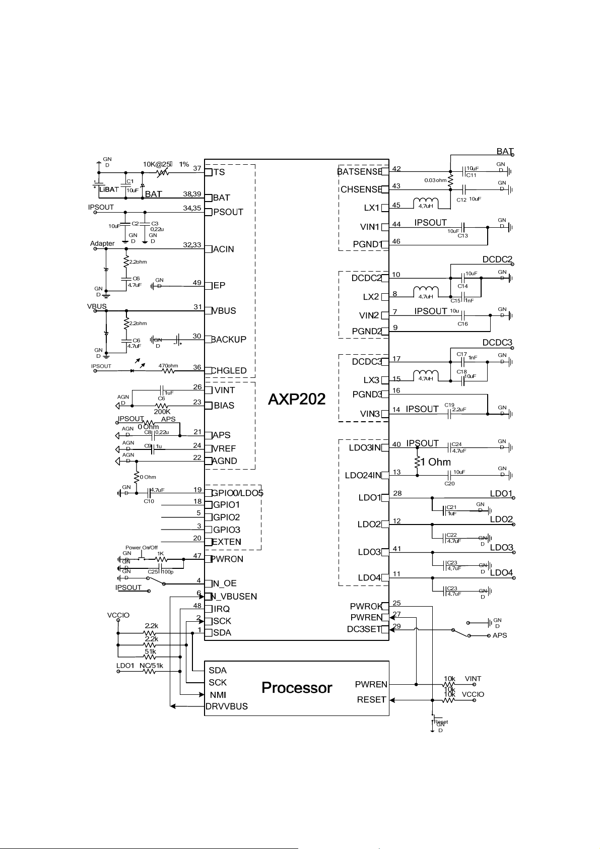
3. Typical Application
AXP202
Single Cell Li-Battery PWM Charger and Power System Management IC
VQ.QW WPPIQPWE CC Confidential Page 4/48
www.x-powers.com

AXP202
Single Cell Li-Battery PWM Charger and Power System Management IC
4. Absolute Maximum Ratings
Symbol Description Value Units
ACIN Input Voltage -0.3 to 11 V
VBUS Input Voltage -0.3 to 11 V
TJ Operating Temperature Range -40 to 130
Ts Storage Temperature Range -40 to 150
T
V
LEAD
ESD
Maximum Soldering Temperature (at leads,10sec)
Maximum ESD stress voltage,Human Body Model
300
>4000 V
℃
℃
℃
PD Maximum Power Dissipation 2100 mW
5. Electrical Characteristics
VIN =5V, BAT=3.8V, TA= 25℃
SYMBOL DESCRIPTION CONDITIONS MIN TYP MAX UNITS
ACIN
VIN ACIN Input Voltage 3.8 6.3 V
I
V
OUT
Current Available Before
OUT
500mV Voltage Drop 2500 mA
Loading BAT
V
ACIN Under Voltage Lockout 3.8 V
UVLO
V
IPS Output Voltage 2.9 5.0 V
OUT
R
Internal Ideal Diode On
ACIN
Resistance
PIN to PIN, ACIN to
IPSOUT
170 mΩ
VBUS
VIN VBUS Input Voltage 3.8 6.3 V
I
V
OUT
Current Available Before
OUT
500 900 mA
Loading BAT
V
VBUS Under Voltage Lockout 3.8 V
UVLO
V
IPS Output Voltage 2.9 5.0 V
OUT
R
Internal Ideal Diode On
VBUS
Resistance
PIN to PIN, VBUS to
IPSOUT
300 mΩ
Battery Charger
V
BAT Charge Target Voltage -0.5% 4.2 +0.5% V
TRGT
I
Charge Current 1200 1800 mA
CHRG
I
Trickle Charge Current 10% I
TRKL
CHRG
mA
V
Trickle Charge Threshold
TRKL
3.0 V
Voltage
VQ.QW WPPIQPWE CC Confidential Page 5/48
www.x-powers.com

AXP202
Single Cell Li-Battery PWM Charger and Power System Management IC
ΔV
T
TIMER1
Recharge Battery Threshold
RECHG
Voltage
Charger Safety Timer
Threshold Voltage
Relative to V
Trickle Mode 40 Min
Termination Time
T
Charger Safety Timer
TIMER2
CC Mode 480 Min
Termination Time
I
End of Charge Indication
END
CV Mode 10% 15% I
Current Ratio
Backup Battery
V
Backup Battery Charge Target
TRGT
2.5 3.0 3.1 V
Voltage
I
Backup Battery Charge
CHRG
50 200 400 uA
Current
I
Current when use Backup
Backup
10 15 uA
Battery
NTC
Charge 2.112 VTL Cold Temperature Fault
Threshold Voltage
Discharge
Charge 0.397 VTH Hot Temperature Fault
Threshold Voltage
VTE NTC Disable Threshold
Voltage
Discharge
Falling Threshold
Hysteresis
Ideal Diode
R
On Resistance(BAT to
ds(on)
75 mΩ
IPSOUT)
TAR GE T
-100 mV
CHRG
mA
0
3.264
V
3.226
0
3.264
V
0.282
0.2 V
SYMBOL DESCRIPTION CONDITIONS MIN TYP MAX UNITS
Off Mode Current
I
OFF Mode Current BAT=3.8V 27 μA
BATOFF
I
SUSPEND
USB VBUS suspend Mode
current
BAT=3.8V,
VBUS=5V,
86 μA
N_VBUSEN=1
Logic
VIL Logic Low Input Voltage 0.3 V
VIH Logic High Input Voltage 2 V
TWSI
VCC Input Supply Voltage 3.3 V
ADDRESS TWSI Address 0x68
f
Clock Operating Frequency 400 1200 kHZ
SCK
tf Clock Data Fall Time 2.2Kohm Pull High 60 ns
VQ.QW WPPIQPWE CC Confidential Page 6/48
www.x-powers.com

AXP202
Single Cell Li-Battery PWM Charger and Power System Management IC
tr Clock Data Rise Time 2.2Kohm Pull High 100 ns
DCDC
f
Oscillator Frequency Default 1.5 MHz
OSC
DCDC2
I
PMOS Switch Current Limit PWM Mode 2300 mA
LIM2
I
V
DCDC3
I
I
V
SYMBOL DESCRIPTION CONDITIONS MIN TYP MAX UNITS
LDO1
V
Available Output Current PWM Mode 1800 mA
DC2OUT
Output Voltage Range
DC2OUT
PMOS Switch Current Limit PWM Mode 1400 mA
LIM3
Available Output Current PWM Mode 1000 mA
DC3OUT
Output Voltage Range
DC3OUT
Output Voltage I
LDO1
LDO1
=1mA
0.7 2.275
0.7 3.5
1.3
-1%
3.3
1%
V
V
V
I
Output Current 30 mA
LDO1
LDO2
V
Output Voltage I
LDO2
I
Output Current 200 mA
LDO2
PSRR Power Supply Rejection Ratio
=1mA 1.8 3.3 V
LDO2
=60mA,1KHz
I
LDO2
TBD dB
eN Output Noise,20-80KHz Vo=3V , Io=150mA 28 μV
LDO3
V
Output Voltage I
LDO3
I
Output Current 200 mA
LDO3
PSRR Power Supply Rejection Ratio
eN Output Noise,20-80KHz Vo=1.8V ,
=1mA 0.7 3.5 V
LDO3
=10mA, 1KHz
I
LDO3
TBD dB
TBD μV
Io=150mA
LDO4
V
Output Voltage I
LDO3
I
Output Current 200 mA
LDO3
PSRR Power Supply Rejection Ratio
eN Output Noise,20-80KHz Vo=1.8V ,
=1mA 1.8 3.3 V
LDO3
=10mA, 1KHz
I
LDO3
TBD dB
18 μV
Io=150mA
LDO5
V
Output Voltage I
LDO5
I
Output Current 50 mA
LDO5
PSRR Power Supply Rejection Ratio
=1mA 1.5 3.3 V
LDO5
=10mA,1KHz
I
LDO5
TBD dB
eN Output Noise,20-80KHz Vo=1.8V, Io=30mA 18 μV
RMS
RMS
RMS
RMS
VQ.QW WPPIQPWE CC Confidential Page 7/48
www.x-powers.com
Single Cell Li-Battery PWM Charger and Power System Management IC
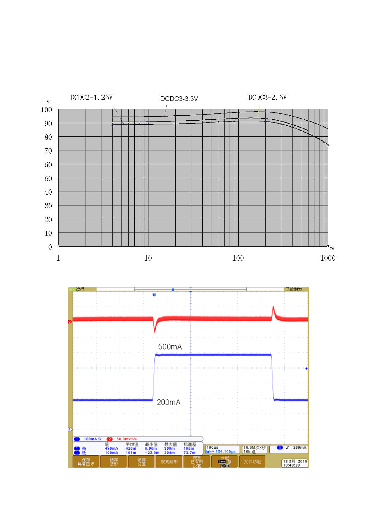
6. Typical Characteristics
DC-DC Efficiency vs. Load(3.8Vin)
AXP202
DC-DC Load Transient(Typical)
VQ.QW WPPIQPWE CC Confidential Page 8/48
www.x-powers.com
AXP202
Single Cell Li-Battery PWM Charger and Power System Management IC
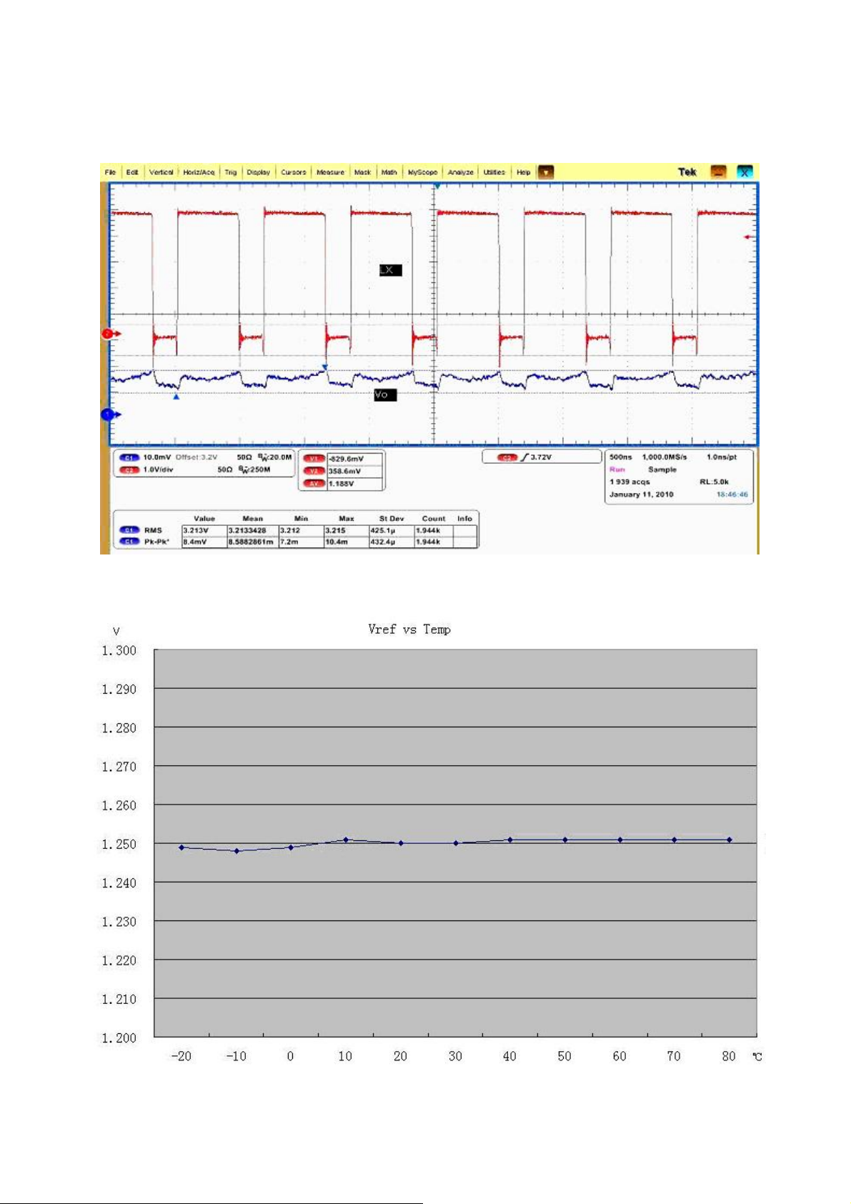
DC-DC Ripple
vs Temperature
V
REF
VQ.QW WPPIQPWE CC Confidential Page 9/48
www.x-powers.com
AXP202
Single Cell Li-Battery PWM Charger and Power System Management IC
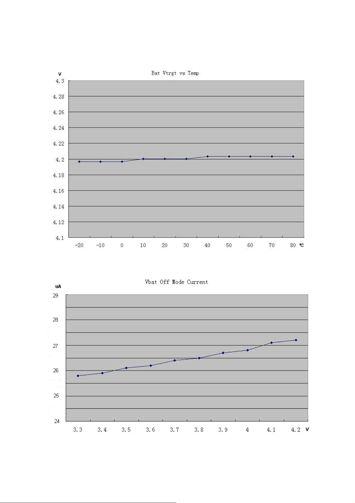
vs Temperature
V
TRGT
Off Mode Current vs V
BAT
VQ.QW WPPIQPWE CC Confidential Page 10/48
www.x-powers.com

AXP202
Single Cell Li-Battery PWM Charger and Power System Management IC
7. Pin Description
Num Name Type Condition Function Description
1 SDA IO Data pin for serial interface,normally it connects a
2.2K resistor to 3.3V I/O power
2 SCK I the Clock pin for serial interface,normally it connects
a 2.2K resistor to 3.3V I/O power
3 GPIO3 IO
4 N_OE I Power output on/off switch
5 GPIO2 IO REG92H[2:0] GPIO 2
6 N_VBUSEN I VBUS to IPSOUT Selection
7 VIN2 PI DCDC2 input source
8 LX2 IO Inductor Pin for DCDC2
9 PGND2 G NMOS Ground for DCDC2
10 DCDC2 I DC-DC2 feedback pin
11 LDO4 O Output Pin of LDO4
REG9EH[7]
GPIO 3
GND:on; IPSOUT:off
GND:IPSOUT select VBUS
High:IPSOUT do not select VBUS
12 LDO2 O Output Pin of LDO2
13 LDO24IN PI Input to LDO2 and LDO4
14 VIN3 PI DCDC3 input source
15 LX3 IO Inductor Pin for DCDC3
16 PGND3 G NMOS GND for DCDC3
17 DCDC3 I Feed back to DCDC3
REG93H[2:0]
19 GPIO0 IO
REG90H[2:0]
20 EXTEN O
21 APS PI Internal Power Input
22 AGND G Analog Ground
23 BIAS IO External 200Kohm 1% resistor
24 VREF O Internal reference voltage
25 PWROK O Power Good Indication Output
26 VINT PO Internal logic power, 2.5V
27 PWREN IO It is the Power domain enable signal
28 LDO1 O
GPIO 1 18 GPIO1 IO
ADC Input
GPIO 0
Low noise LDO/Switch
ADC Input
External Power Enable
LDO1 output,for Host RTC block
VQ.QW WPPIQPWE CC Confidential Page 11/48
www.x-powers.com

Single Cell Li-Battery PWM Charger and Power System Management IC
29 DC3SET IO It set the DCDC3 default voltage
30 BACKUP IO Backup battery pin
31 VBUS PI USB VBUS input
32,33
ACIN PI Adapter input
AXP202
34,35
36 CHGLED O Charger status indication
37 TS I Battery Temperature sensor input or external ADC
38,39
40 LDO3IN O LDO3 input source
41 LDO3 I
42 BATSENSE I PWM Charger Current sense port1
43 CHSENSE O PWM Charger Current sense port2
44 VIN1 PI PWM Charger input source
45 LX1 IO Inductor Pin for PWM Charger
46 PGND1 G NMOS Ground for PWM Charger
47 PWRON I Power On-Off key input
48 IRQ IO IRQ output
49 EP G Exposed Pad, need to connect to system ground
IPSOUT IO Main Battery
input
BAT PO System power source
Output Pin of LDO3
VQ.QW WPPIQPWE CC Confidential Page 12/48
www.x-powers.com
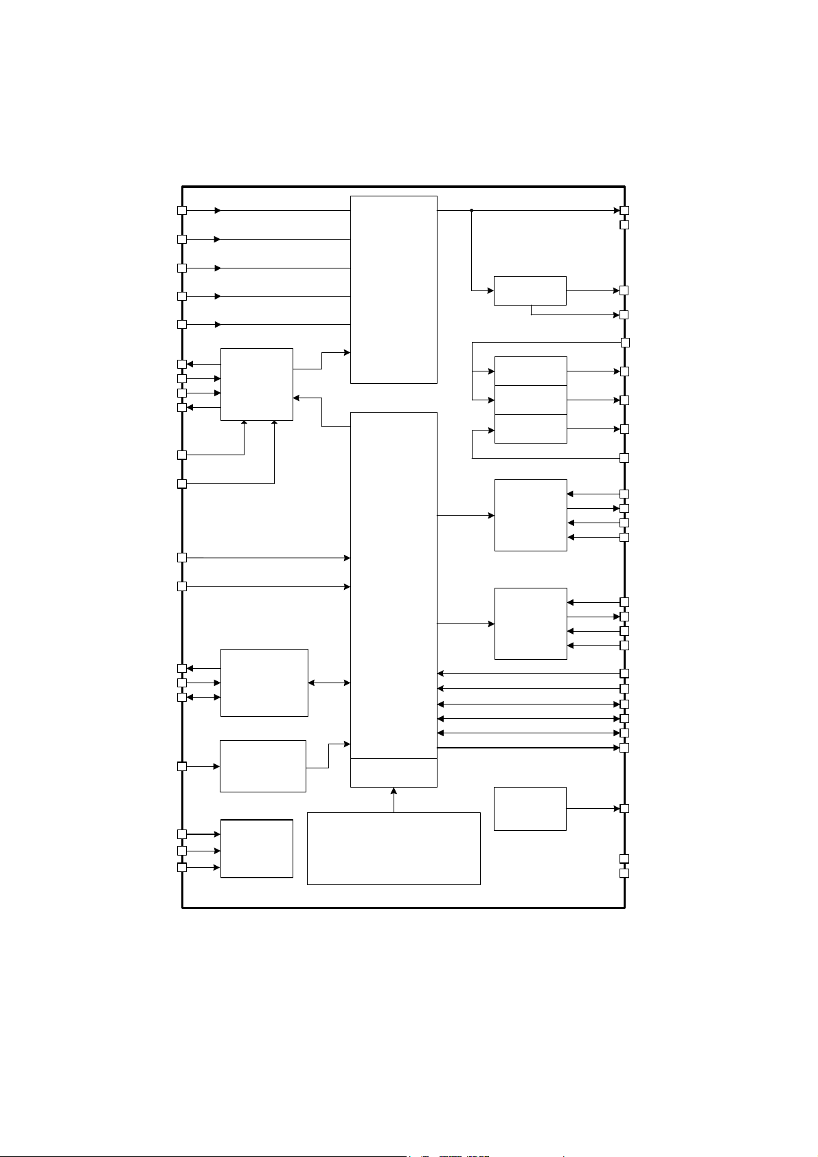
Single Cell Li-Battery PWM Charger and Power System Management IC
8. Functional Block Diagram
AXP202
VBUS
BAT
ACIN
N_VBUSEN
BACKUP
LX1
VIN1
PGND1
CHGLED
BATSENSE
CHSENSE
PWRON
N_OE
IRQ
SCK
SDA
TS
BIAS
VREF
VINT
PWM
Charger
Serial Interface
Bat
Temperature
Monitor
Reference
Voltage
IPS
Control Logic
Register
12 bit ADC
Current Monitor
Voltage Monitor
Temperature Monitor
LDO1
LDO2
LDO4
LDO3
DC-DC2
DC-DC3
Output
voltage
monitor/LBO
IPSOUT
APS
LDO1
N_RSTO
LDO24IN
LDO2
LDO4
LDO3
LDO3IN
DCDC2
LX2
VIN2
PGND2
DCDC3
LX3
VIN3
PGND3
DC3SET
PWREN
GPIO2
GPIO1
GPIO0/LDOio0
EXTEN
PWROK
AGND
EP
VQ.QW WPPIQPWE CC Confidential Page 13/48
www.x-powers.com

AXP202
Single Cell Li-Battery PWM Charger and Power System Management IC
9. Control and Operation
Once AXP202 is powered on, SCK/SDA pin of TWSI will be pulled up to IO Power and then Host can
adjust and monitor AXP202.
Remarks: “Host” here refers to system processor.
Remarks: “External Power” below includes ACIN and VBUS input.
9.1 Power On/Off & Reset
Power Enable Key (PEK)
The Power Enable/ Sleep/Wakeup Key can be connected between PWRON pin and GND of AXP202.
AXP202 can automatically identify the “Long-press” and “Short-press” and then correspond
respectively.
Power on Source
1. ACIN、VBUS and battery
2. N_OE changes from high to low
3. PEK
Power On
System power-on is initiated whenever the following conditions occur:
1. N_OE is low and a valid power source has plugged in (ACIN or VBUS>3.8V, and battery voltage is
higher than power off voltage), AXP202 will be turned on. ( Developer can decide whether AXP202
shall be turned on when there is a valid power source plugging in)
2. N_OE is low and the system is powered off, press PEK can power on AXP202 (In application, Host
Alarm output signal can be connected to PWRON and parallel with PEK. Whenever there is a valid
Alarm signal ((Low Level)), AXP202 can be powered on).
3. When there is a external power source or battery, when N_OE changes from high to low, AXP202
will be turned on.
After power on, DC-DC and LDO will be soft booted in preset timing sequence, and then either Host or
PWREN pin can enable/disable corresponding power.
VQ.QW WPPIQPWE CC Confidential Page 14/48
www.x-powers.com

AXP202
Single Cell Li-Battery PWM Charger and Power System Management IC
Power Off
When you push-and-hold PEK longer than IRQLEVEL, HOST can write “1” into“REG32H [7]” to inform
AXP202 to shutdown, which can disable all power output except LDO1.
System power-off is initiated whenever the following conditions occur:
1. input voltage is too low( Low-Power Protection)
2. Power output voltage is too low due to overload( Overload Protection)
3. Input voltage is too high( Overvoltage Protection)( See more details in chapter “ Intelligent Power
Select”
4. Have waited more than 2S(default) when N_OE changes from hight to low
5. Push PEK longer more than OFFLEVEL( Default 6S), and system will cut off all power output
except LDO1( there is no need for an extra RESET key)
Remarks: With the automatic protection mechanism, AXP202 can protect whole system by preventing
Components from irriversable damage due to system abnormality.
Sleep and wakeup
When the running system needs to enter Sleep mode, REG31H [3] will determine whether one or
several power rails should be disabled or change to other voltage. Wakeup can be triggled by either
PEK signal, or the rising/falling edge of GPIO0、GPIO1、GPIO2、GPIO3 (To be the rising or falling edge,
or both can be programmed by REG90H[7:6]、REG92H[7:6]、REG93H[7:6] and REG95H[7:6]), with all
power rails resume to default voltage in default power on timing sequence.
NOTE: PEK IRQ(REG42H[1])、GPIO0 INPUT Edge IRQ(REG44H[0])、GPIO1 INPUT Edge IRQ
(REG44H[1])、GPIO2 INPUT Edge IRQ(REG44H[2])、GPIO3 INPUT Edge IR(REG44H[3])should
be “Enable” to notify the processor to exit Sleep Mode via IRQ PIN.
See control process under sleep and wakeup modes as below:
VQ.QW WPPIQPWE CC Confidential Page 15/48
www.x-powers.com
 Loading...