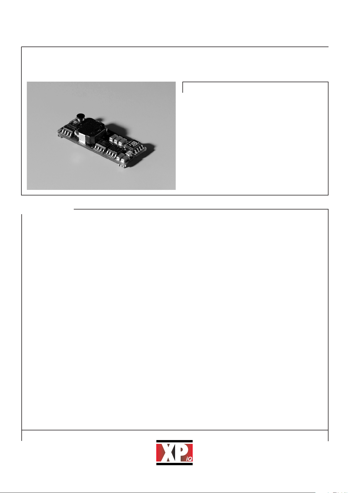
XPiQ inc JWC00605S3V3-L, JWC00605S2V0-L, JWC00605S1V8-L, JWC00605S1V5-L, JWC00603S2V5-L Datasheet
...
High Efficiency
•
Small Footprint
•
Parallelable/Current Sharing
•
Single Control Pin
•
Safety Approvals UL, cUL, TÜV
•
Surface Mount
Input
Input Voltage Range • 3.3 V (3.0 V to 3.6 V) or
5.0 V (4.5 V to 5.5 V)
Input Current • 5.5 A at 3.3 V, 5.0 A at 5.0 V
Start-Up Time • <10 ms
Remote On/Off • Open (logic high) = ON,
Ground (logic low) = OFF
Input Reflected • <250 mV pk-pk
Ripple (V)
Input Reflected • 100 mA pk-pk
Ripple (I)
Output
Output Voltage Range • 1.5 V to 3.3 V - See Table
Output Voltage Adj. • ±10%
Line Regulation • See Tables
Load Regulation • See Tables
Output Voltage • See Tables
Accuracy
Ripple & Noise • 100 mV pk-pk max for 5.0 V in,
80 mV pk-pk max for 3.3 V in
Transient Response • Max deviation of ±10% of Vout
settling to within 90% nominal
in <50 µs for 3 A step load
change
Overcurrent • Operates at 7.5 to 10.0 A
Protection
Short Circuit • Operates in Hiccup mode
Protection
General
Efficiency • See Table
Isolation Voltage • Non-Isolated
Size • 1.300” x 0.530” x 0.248”
Weight • 3.9 g
MTBF • 1,500 000 hours calculated
to Bellcore
Environmental
Operating • 0 °C to +80 °C (See Derating Chart)
Temperature full power to +40°C
Cooling • See derating curve
EMC & Safety
Safety Approvals • Approved to UL 60950,
IEC 60950 and CSA 60950
6 Amps
JWC006-L Series
Non-Isolated DC/DC Converters
Specification
•
•
•
Intelligent Design Quality Product
XPiQ inc.
PH: 508 429.9883
FAX: 800 226.2100
Email: sales@xpiq.com
Holliston, MA 01746 USA
www.XPiQ.com
JWC006-L.qxd 6/6/03 4:40 pm Page 1

Input Output Voltage
(1)
Output Current Efficiency Model
Voltage Minimum Nominal
(1)
Maximum Minimum Maximum Number
1.455 V 1.5 V 1.545 V 80% JWC00603S1V5-L
3.3 V
1.746 V 1.8 V 1.854 V
0.0 A 6.0 A
83% JWC00603S1V8-L
1.940 V 2.0 V 2.060 V 85% JWC00603S2V0-L
2.425 V 2.5 V 2.575 V 88% JWC00603S2V5-L
1.455 V 1.5 V 1.545 V 80% JWC00605S1V5-L
1.746 V 1.8 V 1.854 V 82% JWC00605S1V8-L
5.0 V 1.940 V 2.0 V 2.060 V 0.0 A 6.0 A 84% JWC00605S2V0-L
2.425 V 2.5 V 2.575 V 88% JWC00605S2V5-L
3.200 V 3.3 V 3.400 V 91% JWC00605S3V3-L
OUTPUT VOLTAGE & CURRENT RATINGS JWC006-L
1. Output voltage includes initial setting, input voltage variation, load variation and temperature variation.
2. For parallel operation (4 units max), connect each control pin together but care must be taken to ensure each trace resistance to the
load is approximately the same.
Notes
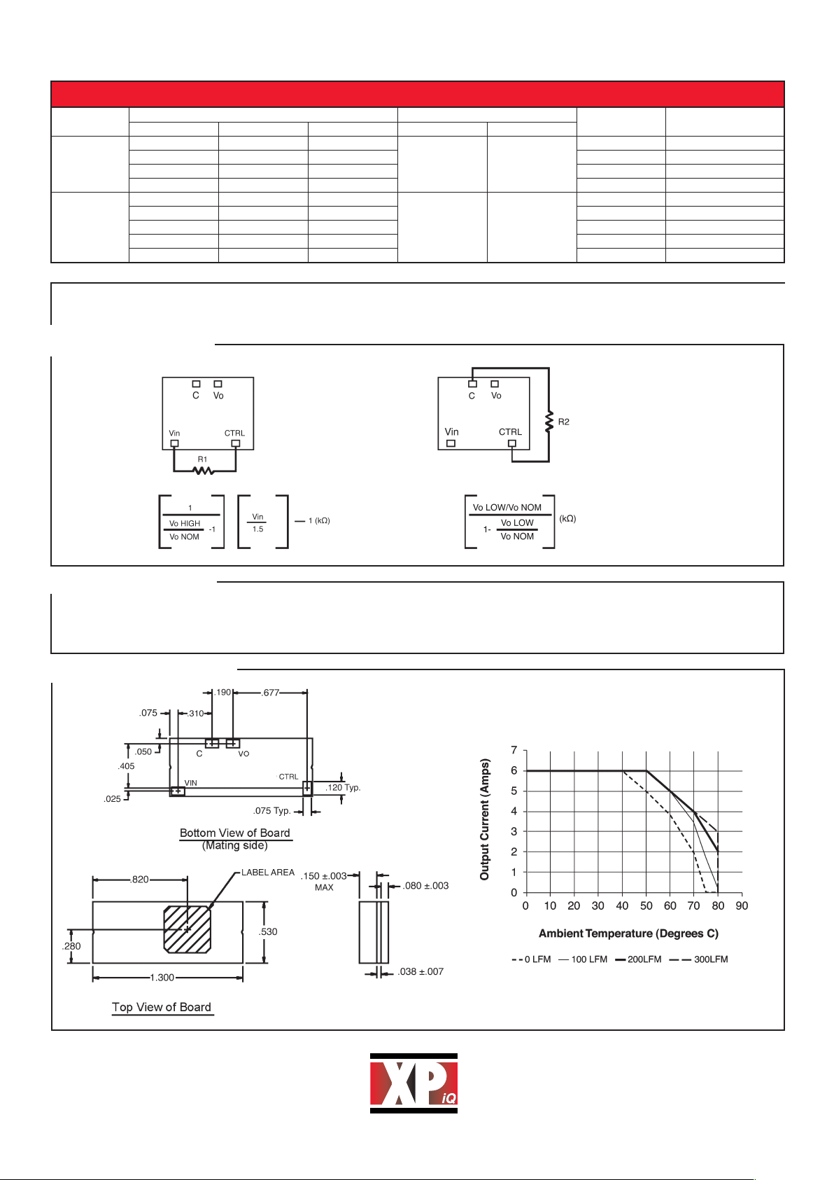
Output Trimming
Mechanical Details
Safety Approvals
These modules are approved to UL60950 3rd edition, CSA60950 3rd edition and IEC60950. These modules are not provided with an
internal fusing. To achieve maximum safety and system protection always use an input line fuse. It is recommended to use a
maximum 10 A normal blow fuse on the ungrounded lead.
Derating Curve JWC00605S3V3-L
•
To trim up: To trim down:
Note: Resistor values
R1 and R2 are in kΩ.
R1 =
x R2 =
PH: 508 429.9883
FAX: 800 226.2100
Email: sales@xpiq.com
Holliston, MA 01746 USA
www.XPiQ.com
JWC006-L.qxd 6/6/03 4:40 pm Page 2
 Loading...