

Page 1
COLOR TELEVISION
TJ# series
TJ2768
TJ2778
TJ306
America
Page 2

CONTENTS
Safety precautions………………………………………………………………………..…
Alignment instructions. ………………………………….………..…………………….…
Working principle analysis of the unit……………………………….………….………….
Block diagram………………………………….. ……………………………………….…………
IC block diagram………………………………………………………………………..……
Wiring diagram ……………………………………………………………..……………...
Troubleshooting……………………………………………………………………………..……
Schematic diagram. ………………………………………………………………………..
1
3
10
11
12
18
19
21
Page 3
Attention: This service manual is only for service personnel to take reference with. Before
servicing please read the following points caref ully.
Safety precautions
After the original service problem has been cor rected, a check should be made of the f ollowing:
FIRE & SHOCK HAZARD
1. Be sure that all components are positioned in such a way as to avoid possibility of adjacent
component shorts. This is especially important on those chassis, which are transported to and from
the repair shop.
2. Never release a repair unless all protective devices such as insulators, barriers, covers, shields,
strain reliefs, and other hardware have been reinstalled per original design.
3. Soldering must be inspected to discover possible cold solder joints, frayed leads, damaged
insulation (including A.C. cord), solder splashes or sharp solder points. Be certain to remove all
loose foreign particles.
4. Check for physical evidence of damage or deterioration to parts and components, and replace if
necessary follow original layout, lead length and dress.
5. No leads or components should touch a receiving tube or a resistor rated at 1 watt or more. Lead
tension around protruding metal surfaces must be avoided.
6. All critical components such as fuses, flameproof resistors, capacitors, etc. must be replaced with
exact factory types. Do not use replacement components other than those specified or make
unrecompensed circuit modifications.
7. After re-assembly of the set always perform an A.C. leakage test on all exposed metallic parts of
the cabinet, (the channel selector knob, antenna terminals, handle and screws) to be sure the set is
safe to operate without danger of electrical shock. Do not use a line isolation transformer during
this test. Use an A.C. voltmeter, having 5000 ohms per volt or more sensitivity, in the following
manner: connect a 1500ohm 10watt resistor, paralleled by a 0.15uF. 150V A.C. type capacitor
between a known good earth ground 9water pipe, conduit, etc. and the exposed metallic parts, one
at a time. Measure the A.C. voltage across the combination of 1500ohm resistor and 0.15uF
capacitor. Reverse the A.C. plug and repeat A.C. voltage measurements for each exposed metallic
part. Voltage measured must not exceed 0.75 volts R.M.S. This corresponds to 0.5 milliamp A.C.
Any value exceeding this limit constitutes a potential shock hazard and must be corrected
immediately.
GRAPHIC SYMBOLS:
It is intended to alert the service personnel to the presence of uninsulated dangerous
voltage that may be of sufficiently magnitude to constitute a risk of electric shock.
It is intended to alert the service personnel to the presence of important safety
information in service literatur e.
X-RADIATION
Too excessive voltage will cause harmful X-ray. To avoid this radiation hazard, the high voltage
should fall within the limitation. The appliance works at AC 120V, 60Hz. The high voltage of zero
1
Page 4

beam current should be within 35KV on condition that the main power(B+) voltage is DC140V . And it
should not exceed 36KV in any condition.
1. Be sure procedures and instructions to all service personnel cover the su bject of X-rays in current
TV is the picture tube. However, this tube does not emit X-rays when the high voltage is at the
factory specified level. The proper value is given in the applicable schematic. Operation at higher
voltages may cause a failure of the picture tube or high voltage supply and, under certain
circumstances, may produce radiation in excess of desirable levels.
2. Only factory specified C.R.T. anode connectors must be used. Degaussing shields also serve as
X-ray shield in color sets. Always re-install them.
3. It is essential that the serviceman has available an accurate and reliable high voltage meter. The
calibration of the meter should be checked periodically against a reference standard. Such as the
one available at your distributor.
4. When the high voltage circuitry is operating properly there is no possibility of an X-radiation
problem. Every time a color chassis is serviced, the brightness should be run up and down while
monitoring the high voltage with a meter to be certain that the high voltage does not exceed the
specified value and that it is regulating correctly. We suggest that you and your service or ganization
review test procedures so that voltage regulation is always checked as a standard servicing
procedure. And that the high voltage r eading be recorded on each customer s invoice.
5. When troubleshooting and making test measurements in a receiver with a problem of excessive
high voltage, avoid being unnecessarily close to the picture tube and the h i gh v oltage compartment.
Do not operate the chassis longer than is necessary to locate t he cause of excessive voltage.
6. Refer to HV, B+ and Shutdown adjustment procedures described in the appropriate schematic
and diagrams. Too excessive voltage will cause harmful X- r ay.
IMPLOSION
1. All direct viewed picture tubes are equipped with an integral implosion protection system, but
care should be taken to avoid damage during installation. Avoid scratching the tube. If scratched,
replace it.
2. Use only recommended factory replacement tubes.
TIPS ON PROPER INSTALLATION
1. Never install any receiver in closed-in recess, cubbyhole or closely fitting shelf space over, or
close to heat duct, or in the path of heated airflow.
2. Avoid conditions of high humidity such as: Outdoor patio installations where dew is a factor. Near
steam radiators where steam leakage is a factor, etc.
3. Avoid placement where draperies may obstruct rear venting. The customer should also avoid the
use of decorative scarves or other coverings which might obstruct ventilat ion.
4. Wall and shelf mounted installations using a commercial mounting kit, must follow the factory
approved mounting instructions. A receiver mounted to a shelf or platform must retain its original
feet(or the equivalent thickness in spacers) to provide adequate are flow across the bottom, blots or
screws used for fasteners must not touch and parts or wiring. Perform leakage test on customized
installations.
5. Caution customers against the mounting of a receiver on sloping shelf or a tilted position, unless
the receiver is properly secured.
6. A receiver on a roll-about cart should be stable on its mounting to the cart. Caution the customer
on the hazards of trying to roll a cart with small caster s acr oss t hresholds or deep pile carpets.
2
Page 5

Alignment instructions
1. General instructions
1.1 The program data should be copied into the EEPROM (N802 M24C16) in this set according to
Standard Sample program data, then execute “Factory Adjustment”. If adopt empty EEPROM,
please preset I2C datum before any debugging.
1.2 If ther e is no special not ice, the unit adjustment should be done on the following conditions:
a. AC power 120V/60Hz.
b. Pre-heat the set for above 30 minutes.
1.3 There is a auto-degaussing circuit inside which could degauss the set automatically within one
second after turn on the power. The auto-degaussing circuit effects on condition that every interval
of turning on the set is longer than 30 minutes at least.
1.4 The magnetized CRT will influence the colour purity and focus. When the inside degaussing
circuit can’t degauss thoroughly then an outside degausser is necessary. Colour purity and focus
adjustment should be executed according to the colour purity and focus adjusts procedures if the
colour purity and focus is not good.
2. Alignment items and procedure
a) B+ voltage check
b) OSD character center adjustment
c) AFT and RFAGC voltage adjustment
d) Focus adjustment
e) Screen-grid voltage adjustment
f) White balance adj ust ment
g) Horizontal and vertical scanning centre and amplitude adjustment
h) Raster correction adjustment
i) HDTV white balance adjustment
j) HDTV Horizontal and vertical scanning centre and amplitude adjustment
k) HDT V raster correction adjustment
Adjustment flow-chat is shown as Fig-1
3
Page 6
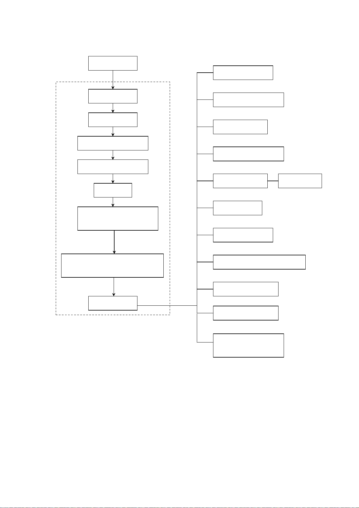
E2PROM copy
High voltage check
B+ voltage
OSD position
AFT adjustment
AGC adjustment
Focus
Screen-grid voltage and w hite
balance adjustment
Centre of scanning amplitude and
raster adjustment
X-ray protection check
Filament voltage
SELF CHECK
Picture parts
Sub-brightness
White balance
Colour purity and convergence
Stereo check
Video/S-VHS/DVD
Check
Auto adjustment
The unit and remote
Control function
Fig-1 Adjustment flow-chart
3. Factory mode adjustment
3.1 Enter factory mode adjustm ent
Press the “factory menu” butt on on t he r emote control, the screen display the factory menu.
3.2 factory menu operation method
Press the channel +/- button to selection the sub menu of factory menu, and press the vol+/- to
enter the sub menu or setting the value.
3.3 exit the factory menu
Press the MENU button again and again; it can exit the factory menu.
4
Page 7

4. Adjustment methods
4.1 B+ voltage adjustment
a. Be sure the voltage AC 120V/60Hz.
b. Connect the digital voltmeter to TP3 and GND of B+ test point, input the US-7 signal, set the
picture control to “standard”, adjust RP501 to let the B+(test point) voltage 140V+/ - 0.3V
c. In the STAND BY t urn off, B+ voltage about 20V
4.2 OSD position adjustment
In the factory menu, select SYS SETTING sub menu, adjust OSD H-POS item, let the character
position to screen display center.
4.3 AFT adjustment
a. IF of tuner (TUNER101) output and TP6 are separate.
b. Input 45.75MHz of frequency and 90db of amplitude signals to TP6
c. Adjust the tunable inductance L110, and measure between the TP4 and GND voltage, until the
TP4 voltage to be 2.5V.
d. Output pin IF of TUNER101 and TP6 bonding pad is normal.
4.4 AGC voltage adjustment
a. Receive 60db split field signal
b. Adjust the potentiometer RP101, and measure the TP5 to GND voltage, until the voltage of TP5
to be 3.5V, t hen noise wave of t he pict ur e point disappears.
4.5 focus adjustment
a. Receive A28 signal, set the picture mode to standar d.
b. Adjust focus potentiometer of FBT, until the B area display best.
4.6 Screen-grid voltage and white balance adjustment
a. Receive US-7 split field signal, the picture mode to “warm”.
b. In the factory menu, select the W HITE BALANCE SETTING menu, fixed the CUT OFF R and
adjust the CUT OFF G and the CUT OFF B, until the white balance is norm al.
c. Select t he color and contrast to 0, select the brightness to 50 in the user menu. In the factory
menu, select the LUMINANCE SETTING menu; adjust the Brightness min, until the back level
voltage about 180V. Adjust the SCREEN potentiometer, until rightmost of gray of the US-7
picture up and down separate.
d. Select the color to 0, the brightness to 50 and the contrast to 100 in the user menu, adjust the
Contrast max, until the eight level g r ay amplitude Vp-p to 100V.
e. Select the color to 0, the brightness and the contrast to 100 in the user menu, adjust the
BRIGHTNESS max, until low right back color of the D-8 picture does not white.
f. In the factory menu, select the WHITE BALANCE SETTING sub menu; adjust the white balance
(color temperature to 12000K+/- 8MPCD, the color coor dinat e to 0.270+/-0.008, 0.283+/-0.008).
4.7 Horizontal and vertical scanning centre adjustment of TV
4.7.1 Horizontal center adjustment
Receive A6 signal, the picture mode to “STANDARD” in the factor y menu, select Horizontal
setting menu, adjust the H PO S, until the picture H-center and screen center accord.
4.7.2 Vertical center adjustment
Receive A6 signal, the picture mode to “STANDARD” in the factory menu, select Vertical
setting menu, adjust the V PO S, until the picture V-center and screen center accord.
4.8 Vertical scanning adjustment
Receive A12 signal, the picture mode to “STANDARD” in the factory menu, select Vertical setting
5
Page 8
menu, adjust the V SIZE, until up and down over scanning of the picture to 8% of the all screen.
4.9 Raster correction and horizontal amplitude adjust ment of TV
Receive white grid of NTSC signal, the picture mode to “STANDARD” in the factory menu, select
horizontal setting menu, adjust the PCC, until the raster distort least, adjust the H SIZE, until r ight
and left over scanning of the picture t o 8% of the all screen.
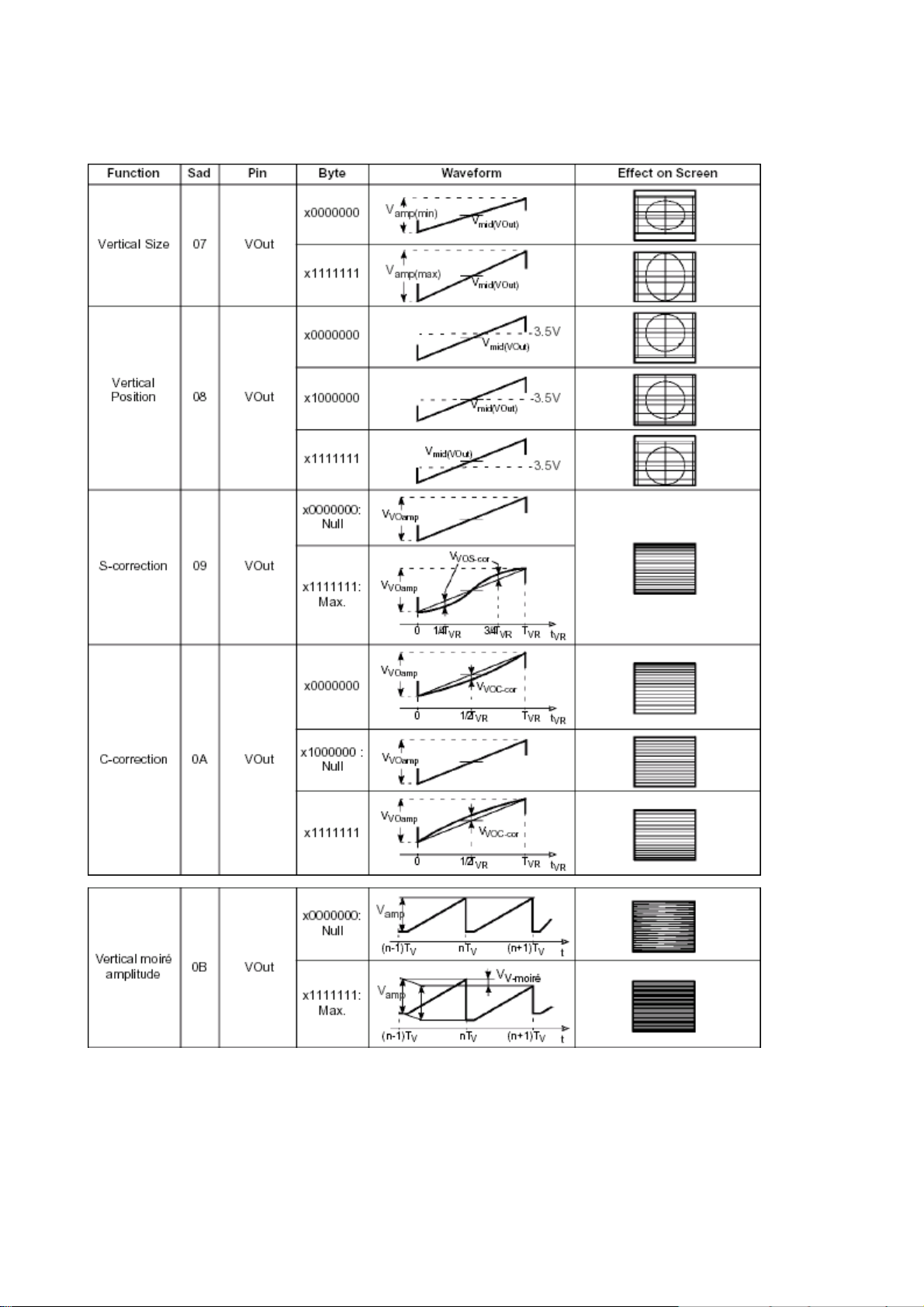
4.10 If the scanning line distortion and raster geometric distortion dissatisfy condition, you can
adjust the factory menu item
SCOR
CCOR
PCAC
PCC
KEYST
PARAL
TCC
BCC
4.11 O utput the max sound of power
Receive the US-7 signal; adjust the volume to max, check the sound power output no less than 2 x
6W.
4.12 White balance and Horizontal and vertical scanning centre and amplitude adjustment of HDTV
The unit has the YPBPR terminal; it can display the HDTV sig nal
Support the HDTV and TIMING of the VG 848 format.
When th e whit e bal an ce ad ju stm ent , t he p ict ur e mod e to STANDARD i n the us er m ode. W hen The
H-V scanning adjustment, set the H-CENTER, H-amplitude, V-CENTER and V-amplitude to 0 in the
user menu.
4.12.1 YPbPr input (480p signal)
a. Whit e balance adj ustment
Input eight level gray of 480p format signal to HDTV YPbPr terminal, the picture mode to
ST ANDARD.
In the factory menu, select the WHITE BALANCE SETTING menu; adjust the white balance (color
temperature to 12000K+/-8MPCD, the color coordinat e t o 0. 270+/-0.008, 0.283+/-0.008).
b. H-CENTER adjustment
Input white grid of 480p format signal to HDTV YPbPr terminal, t he picture mode to STANDARD.
In the factory menu, select Horizontal setting menu, adjust the H POS, until the picture H-center and
screen center accord.
c. V-CENTER adjustment
S-Correction
C-Correction
Pin C ushion Asymmetry Correction
Pin Cushion Correction
Keystone Correction
Parallelogram Correction
Top Corner Correction
Bottom Corner Correction
Support input signal of YPbPr
Signal form at TIMING of the VG848 format
480I 950
480P 978
576I 969
576P 979
1080I/60Hz 972
720P/60Hz 976
1080P/60Hz 970
6
Page 9

In the factory menu, select Vert ical setting menu, adjust the V POS, until the picture V-center and
screen center accord.
d. V-SCANNING adjustment
In the factory menu, select Vertical setting menu, adjust the V SIZE, until up and down over
scanning of the picture to 8% of the all screen.
e. Raster correction and horizontal amplitude adjustment
Receive white grid of NTSC signal, the picture mode to “STANDARD” in the factory menu, select
horizontal setting menu, adjust the PCC, until the raster distort least, adjust the H SIZE, until right
and left over scanning of the picture t o 8% of the all screen.
f. If the scanning line distortion and raster geometric distortion dissatisfy condition, you can adjust
the factory menu item
SCOR
CCOR
PCAC
PCC
KEYST
PARAL
TCC
BCC
4.12.2 YPbPr input (1080I/60Hz format signal)
Adjustment mode to 4.12.1
5. Check point
5.1 check the high voltage
a. Check the second anode and GND connect to the high voltmeter
b. Receive US-7 signal, the picture mode to STANDARD, measure the high voltage to
30.0KV+/-1KV.
c. The brightness and contrast t o m in value, while measure the high voltage no more than 35KV.
5.2 check the CRT Filament voltage
Receive the US-7 signal, the picture mode to STANDARD item, measure the CRT filament voltage
to be 6.3+/-0.2Vrms.
5.3 Check the X-ray protection
a. Receive the US-7 signal, the picture to STANDARD item.
b. Connect TP1 to TP2 point of short circuit; X-ray protection cir cuit must be operation.
5.4 Check the picture part
5.5 Check the sub-brightness
5.6 Check chromatic purity and converge
5.7 Check the VIDEO and audio input/out put
5.8 Check the unit and the remote control function
6. Ex-factory pre-setting
7. Check the supply power (AC 100V-140V/60Hz)
S-Correction
C-Correction
Pin Cushion Asymmetry Correction
Pin Cushion Correction
Keystone Correction
Parallelogram Correction
Top Corner Correction
Bottom Corner Correction
7
Page 10
APPX: horizontal and vertical scanning adjustment diagram
8
Page 11

9
Page 12

Working principle analysis of the unit
The unit is digital frequency conversion processing of 16bit bus control color television, it adopt high
integrity digital processing chip EX-11 of TRIDENT, this chip has a A/D conversion, decoder and
scaler. The MCU is 16bit parallel processor M16C of RENESAS.
The unit adopt frequency composition tuner, it can direct display frequency point of every channel.
The decoder chip have digital comb filter, Y/C processing clean separation, chroma signal and
non-crosstalk brightness signal. It adopts three 10bit A/D and D/A conversion to reality of the picture.
The unit working a singles horizontal frequency, it has two YPBPR terminal inputs and support
multi-high definition format (1080i60, 720p, 1080p and so on), it have picture freeze, dynamic digital
code noise reduction, picture edge enhance, PULL-DOWN, 16:9 mode, timing turn off, rotate, CCD
and V-CHIP functions and so on,
The audio processing adopt application specific IC M61519 of MITSUBISHI, it supports stereo,
treble-bass volume control, volume balance, surround sound and over-bass sound functions and so
on. The unit has two AV inputs, an S terminal input, two YCRCB/YPBPR terminal inputs and a video
output.
The RF signal send to compose tuner TUNER101, its pin11 output 38M of IF signal. After the signal
via pre-intermediate frequency amplifier circuit V101, it sends to the picture SAWF Z102 and sound
SAWF Z101, their are co ntain two filter of single PAL and NTSC, i t be contr olled high-low level of the
pin 75 of MCU output (the pin59 of main board X701). The Z101 output sends to the pin8 of
N101(LA7566) and Z102 output sends to the pin5 and pin6 of N101. The N101 supports PAL and
NTSC system, it be controlled high-low level of MCU (N707, M16C/30620SPGP) output. The level
define as follow:
System X701-pin55 X701-pin53 X701-pin51 X701-pin49
DK (6.5M) 0 1 1 0
I (6M) 1 0 0 1
BG (5.5M) 1 1 0 1
M(4.5M) 0 0 0 0
Note: 1-high level, 0-low level
The pin13 of tuner output video, the video send to the digital chip N700(EX-11). It have VIDEO, two
AV input, S terminal input and two YCRCB/YPBPR input, it through matching circuit to N700. After it
via bus control and digital processing to pin37, pin39 and pin41 of X701 socket output R, G and B
signal (peak value to 0.8V) and the pin 48 and pin48 output V-SYNC and H-SYNC. The V-SYNC
and H-SYNC send to deflection chip N302(STV9118), the pin26 of N302 output H-signal drive the
V301(2SC5422) and H-deflection coil of picture tube. The pin24 of N302 output EW signal for raster
geometry adjustment. After the R, G and B signal of digital board send to the pin1, pin3 and pin5 of
pre-video amplifier N801(STV9211) form pin14, pin16 and pin18 output to CRT board. The N401 of
CRT board to R,G,B signal amplify to peak value(about 100V), it send to c athode of the pictu re tube.
The SIF of the SAWF output send to stereo decoder NS01(LA72700), then it output L/R of audio.
The L/R audio of TV, AV/S input and YCRCB/YPBPR input send to sound processor N601(M61519).
Through BUS control of N707 to select processing of N601 signal channel, the pin25 and pin18 of
N601 output L/R audio send to N602 (TA8256BH), the pin8 and pin12 of N602 output L/R audio
drive speaker. In the mute state, the N707 send high level to the pin5 of N602, but the power
amplifier without signal.
10
Page 13

0
bPr1YPbPr2
t
R
N
Block diagram
LA72700
I2C
NS01
SIF
N101
IF
LA7566
Clamp
Blanking
R
G
B
I2C
L/R
N801
PRE-VIDEO
AMP.
STV9211
I2C
N707
CPU
M16c/30620SPGP
AV ou
AV2
L
L
I2C
2
I
R
C
L
SOUND PROCESSING
R
G
B
R
N601
M61519
BOARD
LM2423
DDY
STV9118
ROM
24C16
L
CRT
302
YP
R
AV1/S
L
STEREO DECODER
AVOUT-V
TUNER
AV1(video)/Y
C
AV2(video)
YPbP
r1
SOUND SAWF
PICTUR SAWF
Z1
N700
ND decodor, scaler
Trident
EX-11
2
CVBS
YPbP
r2
I2C
EMST
16161
EMST
16161
R
L
R
R
G
B
SOUND
AMP.
TA8256
CRT
H-AMP
2SC5422
V-AMP
LA78041
L
11
Page 14

IC block diagram
1. LA7566
10: AFT output 19: SIF output
9: AGC output 1: TV audio output
5, 6: picture IF input 13: TV video output
8: sound IF input 3: 9V
12
Page 15

2. EX-11
185: S-C input 187: Pb2 input
196: AV1-V/S-Y input 180: Pr2 input
197: AV2-V input 14: SCL
198: TV-V input 16: SDA
200: Y1(PbPr) input 190, 191: AVOUT-V output
186: Pb1 input 28: B output
179: Pr1 input 29: G output
202: Y2(PbPr) input 30: R output
34: H-SYNC output 31: VM output
37: V-SYNC output 9, 168 and so on: 1.8V
36: CLAMP output 15: 5V-1
13
Page 16

3. M61519FP
39: AV2 audio-L input 7: AV1/Saudio-R input
4: AV2aduion-R input 35: AVOUT audio-L output
6, 37: TV audio input 8: AVOUT audio-R output
38: YPbPr1audio-L input 11: audio- L output
5: YPbPr1audio-R input 19: audio-R output
40: YPbPr2audio-L input 22: CLOCK
3: YPbPr2audio-R input 21: DATA
36: AV1/Saudio-L input 20: 9V
14
Page 17

4. STV9118
2: V-SYNC input 24: pincushion correction output
1;V-SYNC input 25: X-ray protection input
18: Vertical high voltage compensation input 31: SDA
17:Horizontal high voltage compensation input 30: SCL
26: horizontal signal output 29: 12V
23: vertical signal output
15
Page 18

5. STV9211
1: R input 1: ABL
3: G input 5: B input
13: SDA 16: G output
19: CLAMP 14: B output
20: BLANK 7, 17: 5V
18: R output 12: SCL
16
Page 19

6. LA72700V
5: SIF input 25: R output
11: SDA 26: L output
12: SCL 31: 9V
17
Page 20

Wiring diagram
18
Page 21

Trouble shooting
f
y
n
y
l
N
N
f
N
No N
1. No raster, No picture and No sound
Check the indicator
Press the power button
o signal
Check if the pin10 o
CPU has low-level
output
Check if it has X-ra
protection
Check if it has
vertical protectio
circuit
Light
Turn on
Check if the N802 is
normal
o-light
Check the FU501
Measure if the C516 is
about 150V
Check the N501, N502
and peripheral circuit
Check the suppl
power
Check the D501
and periphera
circuit
2. Picture, but w i t hout sound
Check if the N602 output
Check if the pin2 and pin4 o
sound amplifier output
Check the supply power, the
pin5 of mute is low level
Yes
Yes
Speaker damage
o
Check if sound-processing
601 is normal.
19
Page 22

3. Sound, but wit hout pi cture
p
p
p
d
N
No N
Without raster Raster
It has sound, but without picture
Check if the
in26 of N302
has H-frequency
Check if the
V301 is damage
Abnormal
Check B+
Check if the H-V
circuit is normal
ormal
Check the FBT
Check the filament
voltage of CRT
board
Check if the digital
rocessing board has
RGB and H-V sync
output
Check if the digital
rocessing board has
RGB output
Check the N801 an
peripheral circuit
Check the N700
and peripheral
circuit
o
Check the digital
20
Page 23

Schematic diagram
21
Page 24

Page 25

Page 26

5
SC1
SD1
5V-1_DPTV
D D
C783
0.1uF
0
R729
C C
B B
MD[0..31]
DQM[0..3]
A A
MA[0..10]
NKL
CS0#
RAS#
CAS#
R774 68
R770 68 RN702
C770
68pF
RST
N700A
MD0
53
MD1
MD2
MD3
MD4
MD5
MD6
MD7
MD8
MD9
MD10
MD11
MD12
MD13
MD14
MD15
MD16
MD17
MD18
MD19
MD20
MD21
MD22
MD23
MD24
MD25
MD26
MD27
MD28
MD29
MD30
MD31
DQM0
DQM1
DQM2
DQM3
5
MD0
55
MD1
56
MD2
58
MD3
62
MD4
64
MD5
66
MD6
68
MD7
69
MD8
71
MD9
72
MD10
74
MD11
78
MD12
80
MD13
82
MD14
84
MD15
124
MD16
126
MD17
128
MD18
130
MD19
134
MD20
136
MD21
137
MD22
139
MD23
140
MD24
142
MD25
144
MD26
146
MD27
150
MD28
152
MD29
153
MD30
155
MD31
59
DQM0
75
DQM1
133
DQM2
149
DQM3
SVP-EX_208
NKL
C772
68pF
12
13
15
V5SF
RESET
TESTMODE
SVP-EX [208]
DQS060DQS176DQS2
DQS3
132
148
NKL
4
A4
A5
16
SDA
A7A1A6
RN701
22x4
7 8
14
165
SCL
5 6
164
A_D7
A_D6
3 4
163
A_D5
1 2
162
A_D4
161
A3
7 8
160
A_D3
A_D2
A2
5 6
159
A_D1
A0
3 4
158
A_D0
22x4
1 2
(1 of 2)
MA1185MA1087MA988MA890MA791MA693MA594MA496MA398MA299MA1
MA7
MA8
MA9
MA6
MA5
MA10
4
MA4
MA3
101
MA1
MA2
TP_C30
MA0
102
MA0
TP1
170
171
RD#
MCK0
106
107
172
ALE
WR#
MCK0#
CS0#
CS1#
109
111
3
RN703
1 2
3 4
5 6
7 8
173
174
INT#
MPUCS0N
RAS#
CAS#
MVREF
113
114
116
TP2
TP_C30
3
22x4
MPUCS0N
R711 0_DNS
18
17
P_17
FLD/IO
MPUGPIO0
MPUGPIO1
VDDR
VSSR
VDDM
VDDM
VDDM
VDDM
VDDM
VDDM
VDDM
VDDM
VDDM
VDDM
VDDM
VDDM
VSSM
VSSM
VSSM
VSSM
VSSM
VSSM
VSSM
VSSM
VSSM
VSSM
VSSM
VSSM
WE#
CLKE
BA0
BA1
118
R710 0_DNS
120
121
123
A[0..7]
Option
157
156
115
117
151
145
135
129
112
110
100
95
79
73
63
57
147
143
131
127
108
105
97
92
81
77
65
61
Option
BA
CLKE
WE#
2
VCC_3
I2C Address:
10K
7E/7F
I2C
Address:
7C/7D
Not
Populated
CS
1K_DNS
VCC_3
R732
10K
R731
INPUT
MPUGPIO0
01
OUTPUT
MPUCS0N
0
RD
WR
ALE
INT
10K_DNS
MPUGPIO0
MPUGPIO1
R781
R782
VDDM
110
*CS1N is not a input or output pin
CS1N=0: SVP-EX CPU access enabled
CS1N=1: SVP-EX CPU access disabled
VDDM VDDM
C767
0.1uF
C764
0.1uF
Title
Schematict Name Rev
A
Size
2
10K
R769
R768
1K
SVP-EX 1 of 2
FB420 G
16
of
Date:Sheet
Tuesday, Apr il 0 5, 2005
1
CS1N
1
Page 27

5
MLF1
PLF2
C794
0.1uF
C786
0.1uF
AGND
67
83
89
119
125
141
168
54
70
86
122
138
154
169
208
SVP-EX_208
C795
20pF
R702 10K_DNS
N700B
3
MLF1
6
PLF2
9
VDDC
VDDC
VDDC
VDDC
VDDC
VDDC
VDDC
VDDC
8
VSSC
VSSC
VSSC
VSSC
VSSC
VSSC
VSSC
VSSC
1
XTALO
XTALI
C793 2700pF
C785 2700pF
PDVDD
C7A3
0.1uF
PDVSS
PAVDD
C7B0
0.1uF
PAVSS
5
Option
52
EX11/12 USE
EX32 USE
R704
10K_DNS
Option
R706
10K
VDDC
VDDH
VSSH
VSSC
41
43
P_4444P_4545P_4646P_4747P_4848P_4949P_5050P_5151P_52
P_3737P_3838P_3939P_4040P_41
P_4242P_43
SVP-EX [208]
(2 of 2)
PAVSS
PDVSS
AVSS_ADC1
AVSS3_BG_ASS
AVSS_ADC2
AVSS_ADC3
VSSH
VSSL
189
182
176
AVSS_ADC3
AVSS3_BG_ASS
AVDD_ADC3
AVSS_ADC3
167
20
VSSH
103
VSSL
VSSH
AVDD_ADC1
AVSS_ADC1
AVDD_ADC2
AVSS_ADC2
L710
C7A1
0.1uF
C7A9
0.1uF
C7A7
0.1uF
PAVSS2
4
7
PAVSS2
PAVSS1
PAVSS1
207
205
PDVSS
PAVSS
PAVDD1
PAVSS1
PAVDD2
PAVSS2
193
AVSS_ADC1
MLF1
PLF2
AVSS_ADC2
R708 10
36
PAVDD2
2
5
PAVDD2
PAVDD1
C732
10uF/16V
PAVDD
PAVDD1
206
PAVDD
1 2
VD3_3
D D
VD1_8
C C
G700
14.318MHz
C796
20pF
VL1_8
L704 150_Ohm_600mA
B B
1 2
C729
10uF/16V
L707 150_Ohm_600mA
1 2
C727
10uF/16V
L711 150_Ohm_600mA
1 2
C734
A A
10uF/16V
L713 150_Ohm_600mA
1 2
C743
10uF/16V
4
ADVDD33
AVSS33_1
PDVDD
AVDD_ADC1
AVDD3_AVSP2
AVDD_ADC2
AVDD_ADC3
204
192
188
181
175
PDVDD
AVDD_ADC2
AVDD_ADC1
AVDD_ADC3
AVDD3_AVSP2
L705
1 2
C742
150_Ohm_600mA
10uF/16V
L708
1 2
C740
150_Ohm_600mA
10uF/16V
VA1_8
150_Ohm_600mA
4
166
VDDH
19
AGND
R775
AVDD33
VDDH
AVSS33_3
VDDL
104
VDDL
VDDH
VA1_8
VA1_8
560
AGND
AIN_HS
AIN_VS
P_2121P_2222P_2323P_2424P_2525P_2626P_2727P_2828P_2929P_3030P_3131P_3232P_3333P_3434P_3535P_36
Y_G1
PB_B1
PR_R1
Y_G2
PB_B2
PR_R2
CVBS_OUTP
CVBS_OUTN
CVBS1
CVBS2
CVBS3
AIN_N1
AIN_N2
AIN_N3
VREFP_1
VREFN_1
VREFP_2
VREFN_2
VREFP_3
195
194
184
183
178
VDDL
C760
0.1uF
VSSL
AGNDAGND
VDDC
VSSC
AVDD3_AVSP2
C7A8
0.1uF
AVSS3_BG_ASS
C
VREFN_3
177
VREFN_3
VREFP_3
VREFN_2
VREFP_2
VREFN_1
VREFP_1
VD1_8
10
11
200
186
179
202
187
180
190
191
196
197
198
185
199
201
203
PRELIMINARY
V-sync
CLAMP
H-sync
VM
R_
G_
B_
R773
0/10K
When use EX12,use 0ohm;
When use EX22,use 10Kohm.
H-DSUB
V-DSUB
Y
Pb
Pr
Y_G2
PB_B2
PR_R2
CVBS_OUTP
CVBS_OUTN
CVBS1_
CVBS2_
CVBS3_
C_
AIN_N1
C766
0.1uF
AIN_N2
AIN_N3
L706
1 2
C704
10uF/16V
L712
1 2
C741
10uF/16V
AIN_N2
AIN_N3
VD1_8
150_Ohm_600mA
VD3_3
150_Ohm_600mA
3
C749 0.1uF
CVBS1_
R759
75
CVBS1_G
C750 0.1uF
CVBS2_
R760
75
CVBS2_G PB_B2_G
C751 0.1uF
CVBS3_
R761
75
CVBS3_G
C746 0.1uF
C_
R756
75
C_G
AVDD33
ADVDD33
AVSS33_3
AVSS33_2
AVSS33_1
AIN_N1
CVBS_OUTP
CVBS_OUTN
AGND
3
C712
0.1uF
CVBS1_G
CVBS2_G
CVBS3_G
C_G PR_R2_G
Place this
R790
resistor close to
EX chip
1K
AGND
10uF/16V
C7A2
30pF
C799 0.1uF
TV Y G-DSUB
TV_G
VIDEO1
VIDEO1_G
VIDEO2/Y-YC Pr
VIDEO2/Y_G
C-YC
VD3_3
C718
0.1uF
C733
VIDEO_OUT
R789
75
VIDEO_OUT_G
2
Y
Pb
Pb
Pr
C780
B
C720
10uF/16V
VREFP_2
0.1uF_DNS
AVSS_ADC2
C761
0.1uF
L709
1 2
C788
Title
VDDH
C710
VREFP_1
0.1uF_DNS
AVSS_ADC1
2
C719
0.1uF
C789
AIN_N2
R791
1K
AGND
C774
0.1uF
VSSH
C782
0.1uF
AIN_N2 AIN_N3
C791
0.1uF
0.1uF
VREFN_1
C781
0.1uF
0.1uF
Y_G1_G
PB_B1_G
PR_R1_G
Place this
resistor close to
EX chip
C763
C762
0.1uF
0.1uF
Schematict Name Re v
Size
1
C753 0.1uF
Y_G2
R763
75
Y_G2_G
C748 0.1uF
PB_B2
R758
75
C745 0.1uF
PR_R2
R755
75
PR_R2_G
VD3_3
150_Ohm_600mA
VREFN_2
C779
0.1uF
AIN_N3
R793
1K
AGND
C765
C768
0.1uF
0.1uF
SVP-EX 2 of 2
FB420 G
26
of
VREFP_3
0.1uF_DNS
C778
0.1uF
AVSS_ADC3
Y_G2_G
PB_B2_G
Place this
resistor close to
EX chip
C776
C792
0.1uF
0.1uF
Tuesday, April 05, 2005
Date:Sheet
1
B-DSUB
R-DSUB
C787
C784
0.1uF
VREFN_3
VD1_8
C777
0.1uF
Page 28

5
4
3
2
1
BA
WE#
CAS#
D D
RAS#
NKL
R709 33
R705 33
R703 33
R701 33
R700 33
BA_
WE_
CAS_
RAS_
NKL_
MA[0..10]
CLKE
C C
VCC3_M
B B
R707 33
35
15
16
17
MD0
MD1
MD2
MD3
MD4
MD5
MD6 MD17
MD7
MD8
MD9
MD10
MD11
MD12
MD13
MD14
MD15
11
12
39
40
42
43
45
46
48
49
13
38
44
25
2
DQ0
3
DQ1
5
DQ2
6
DQ3
8
DQ4
9
DQ5
CLK
RAS
CAS
WE
DQ6
DQ7
DQ8
DQ9
DQ10
DQ11
DQ12
DQ13
DQ14
DQ15
VDDQ
7
VDDQ
VDDQ
VDDQ
VDD
1
VDD
CS
18
CLKE_
19
KM416S1020B
MA10
BA
MA9
MA8
MA7
MA6
MA5
MA4
MA3
MA2
MA1
MA0
CKE
UDQM
LDQM
N.C.
N.C./RFU
VSSQ
VSSQ
VSSQ
VSSQ
VSS
VSS
N701
20
32
31
30
29
28
27
24
23
22
21
34
36
14
33
37
10
4
47
41
50
26
MA10
MA9
MA8
MA7
MA6
MA5
MA4
MA3
MA2
MA1
MA0
DQM1
DQM0
VCC3_M
MD23
MD22
MD21
MD20
MD19
MD18
MD16
MD24
MD25
MD26
MD27
MD28
MD29
MD30
MD31
11
12
39
40
42
43
45
46
48
49
13
38
44
25
2
3
5
6
8
9
7
1
DQ0
DQ1
DQ2
DQ3
DQ4
DQ5
DQ6
DQ7
DQ8
DQ9
DQ10
DQ11
DQ12
DQ13
DQ14
DQ15
VDDQ
VDDQ
VDDQ
VDDQ
VDD
VDD
35
17
CLK
16
RAS
15
CAS
18
19
WE
CS
KM416S1020B
MA10
BA
MA9
MA8
MA7
MA6
MA5
MA4
MA3
MA2
MA1
MA0
CKE
UDQM
LDQM
N.C.
N.C./RFU
VSSQ
VSSQ
VSSQ
VSSQ
VSS
VSS
N702
20
32
31
30
29
28
27
24
23
22
21
34
36
14
33
37
10
4
47
41
50
26
MA10
MA9
MA8
MA7
MA6
MA5
MA4
MA3
MA2
MA1
MA0
DQM3
DQM2
VCC3_M
VCC3_M
VCC3_M
VCC3_M
C722
1000pF
C702
0.1uF
C701
1000pF
C726
0.1uF
C775
1000pF
C700
0.1uF
1000pF
C790
0.1uF
C709
C773
1000pF
C707
0.1uF
C711
0.1uF
C723
100uF/16V
C708
1000pF
C703
100uF/16V
CS0#
MD[0..31]
DQM[0..3]
MD[0..31]
DQM[0..3]
SDRAM
DECOUPLING
VCC3_MVCC3
CAPACITORS
L700
C728
A A
22uF/16V
C797
0.1uF
Title
SDRAM 1MX16
Schematict Name Rev
FB420 G
A
Size
5
4
3
36
2
of
Date:Sheet
Thursday, March 31, 2005
1
Page 29

5
4
3
2
1
3.3V POWER FOR SDRAM
3.3V_1
D D
L714
C757
C7B5
100uF/16V
0.1uF
N703
SS6117A-1.8
3
IN
GND
OUT
2
L720
VA1_8
C7A6
0.1uF
C739
22uF/16V
1
3.3V_2
L717
C7B1
0.1uF
L716
C755
22uF/16V
3.3V POWER FOR SVP-EX
VL1_8
N704
SS6117A-1.8
3
IN
C C
OUT
2
GND
1
L721
C737
0.1uF
C735
22uF/16V
L718
C769
0.1uF
VD3_33.3V
C713
22uF/16V
VCC3
C7A0
0.1uF
VDDM
C736
22uF/16V
VD1_8
N705
SS6085-1.8
3
IN
B B
4
GND
GND
1
OUT
2
C705
0.1uF
C706
22uF/16V
3.3V_3
L719
3.3V POWER FOR SVP-EX
L715
C7C0
0.1uF
C759
22uF/16V
C758
22uF/16V
VCC_3
C7B9
0.1uF
L722
5V-1 5V-1_DPTV
D702 1N4148
A A
Title
POWER
Schematict Name Rev
FB420 G
A
Size
5
4
3
46
2
of
Date:Sheet
Tuesday, Apr il 0 5, 2005
1
Page 30

5
4
3
2
1
LR-MUTE
X700 HEADER_24X2
W-MUTE
SDA-EEP
D D
SCL-EEP
PAGE-EEP
CNVSS
RESET-CPU
TX
RX
5V-1
CLK1
CTX1/RTX1
HOLD
WR_
3 4
5 6
7 8
9 10
11 12
13 14
15 16
17 18
19 20
21 22
23 24
25
27 28
29
C C
SDA
SCL
31 32
33 34
35 36
R-OUT
G-OUT
B-OUT
37 38
39 40
41 42
21
SCL_CPU
SDA_CPU
3.3V
ON-TIMER
REMOTE
KEY
5V-1
Power
FLASH
26
30
V_Protect
X_Ray
5V-1_CPU
SDA
R7A5
SCL
10K
S-TRAP4
S-TRAP3
S-TRAP2
S-TRAP1
PAL/N
AFT
TV_G
VIDEO1_G
VIDEO1
AIN_N3
V-DSUB
H-DSUB
B-DSUB
G-DSUB
R-DSUB
TV_G
TV
TV
VIDEO1_G
VIDEO1
AIN_N3
Rotation
SVM
X701 HEADER_17X2
3 4
5 6
7 8
9 10
11 12
13 14
15 16
17 18
19 20
21 22
23 24
25
27 28
29
31 32
33 34
21
VIDEO OUT_G
VIDEO2/Y_G
26
AIN_N2
30
Pr_1
Pb_1
Y_1
R762
75
R757
75
C744 0.1uF
C747 0.1uF
C752 0.1uF
R754
75
TV-Hsync
3.3V_1
3.3V_2
3.3V_3
VIDEO_OUT_G
VIDEO_OUT
YC/VIDEO
C-YC
VIDEO2/Y_G
VIDEO2/Y-YC
AIN_N2
Pr_1#
Pb_1#
Y_1#
43 44
BLANKING
CLAMP
45 46
47 48
GND_CPU
B B
R764
R765
R766
75
75
75
C7B4
10pF
L701
L702
L703
10pF
C7B6
10pF
C7B7
C7B8
10pF
G-OUT
B-OUT
R_
R_ R-OUT
G_
G_
B_
B_
C7B2
C7B3
10pF
10pF
A A
GND_CPU
5
V-sync
H-sync
SDA
SCL
0
R798
0
R7A1
VM
R7A6
100
5V-1
R7A0
4.7K
5V-1
R7A2
4.7K
R771
2.2K
V700
MMBT3906
(PNP)
R799
R7A3
R772
1K
C7Y3 0.1uF
C7Y4 0.1uF
Pr_1#
PR_2
R7Y3
5V-1
C7Y2
47uF/16V
0_DNS
C7Y5 0.1uF
NY01
1
2
3
4
5
R7Y4 100
5V-1
C7Y1
1000pF
R7Y1
R7Y2
0_DNS
0_DNS
0
SD1
0
SC1
SELECT
TJC3_5
X702
SVM
Y_1#
Y_2
Pb_1#
PB_2
1
IN
2
S1A
3
S2A
4
DA
5
S1B
6
S2B
7
DB
GND8DC
FSAV330
VCC
S1D
S2D
S1C
S2C
/EN
16
15
14
13
12
DD
11
10
9
Y
Pb
Pr
Title
INTERFACE CONNECTOR
Schematict Name Re v
B
Size
4
3
2
FB420 G
Wednesday, April 06, 2005
56
Date:Sheet
of
1
Page 31

5
4
3
2
1
5V-1_CPU
R78510K
V701
MMBT3904_DNS
R787
1K_DNS
Optional
GND_CPU
E C
Power
D D
100
LR-Mute
W-Mute
PAL/N
R784
100
R743
R783 100_DNS
R780 100
OPTION
75
100
R7A4
10K
GND_CPU
PAGE-EEP
AD7
AD6
AD5
AD4
AD3
AD2
AD1
AD0
GND_CPU
R779
R778
47
R777 100
100
R720
100_DNS
R718
OPTION
R719 10K
SELECT
100
R717
R726 100
R725 100
R724 100
5V-1_CPU
100_DNS
R723
R721 100_DNS
OPTION
PAGE-EEP
ON-Timer
BLANKING
D701
C C
B B
GND_CPU
V_Protect
5V-1_CPU
R716
10K
KEY
100pF
GND_CPU
C725
YC/VIDEO
X_Ray
AFT
5V-1_CPU
C724
100pF
Key_IN_LED
GND_CPU
76
77
78
79
80
81
82
83
84
85
86
87
88
89
90
91
92
93
94
95
96
97
98
99
100
P1_2
P1_1
P1_0
P0_7/AN0_7
P0_6/AN0_6
P0_5/AN0_5
P0_4/AN0_4
P0_3/AN0_3
P0_2/AN0_2
P0_1/AN0_1
P0_0/AN0_0
P10_7/AN7
P10_6/AN6
P10_5/AN5
P10_4/AN4
P10_3/AN3
P10_2/AN2
P10_1/AN1
Avss
P10_0/AN0
Vref
Avcc
P9_7/ADTRG
P9_6
P9_5
P9_4/DA11P9_2/TB2in3P9_1/TB1in4BYTE6CNVss7P8_6/Xcout9Reset10Vss12Xin
Rotation
S-TRAP1
S-TRAP2
S-TRAP3
S-TRAP4
R722 100
Option
R727 0_DNS
R728 0_DNS
R730 0_DNS
R733 0_DNS
5V-1_CPU
R715 220
D700 HZ4A2
R713 1K
C721 1000pF
C714 10uF/16V
A A
GND_CPU
R714
8.2K
C715
47uF/16V
MMBT3906
B
C E
B
P1_474P1_3
P9_3/DA0
2
V702
RESET-CPU
TP3
AD0
R78610K
73
P1_7/INT571P1_6/INT472P1_5/INT3
P9_0/TB0in
5
R734
4.7K
5V-1_CPU
TP4
AD1
TP8
TP5
AD2
A1A3A0
TP9
TP6
TP7
AD5
AD6
AD3
AD4
A4A4A3A1A2
A5A5A7
A6
P2_0/A0/D070P2_1/A1/D169P2_2/A2/D268P2_3/A3/D367P2_4/A4/D466P2_5/A5/D565P2_6/A6/D664P2_7/A7/D7
M30620SPGP
P8_7/Xcin
Xout
8
11
CNVSS
R735
GND_CPU
GND_CPU
G701
10MHz
C798
15pF
4.7K
TP10
AD7
63
N707
13
5V-1_CPU
62
Vss
Vcc114P8_5/NIM
C7A4
15pF
RESET-CPU
5V-1_CPU
GND_CPU
61
P3_0/A8
15
R788
4.7K
A[0..7]
60
59
Vcc2
P3_1/A9
P8_3/INT117P8_2/INT018P8_0/TA4out20P7_7/TA3in
P8_4/INT216P8_1/TA4in
P3_2/A1058P3_3/A1157P3_4/A1256P3_5/A1355P3_6/A1454P3_7/A1553P4_0/A1652P4_1/A17
P6_0/CTS0/RTS0
P6_4/CTS1/RTS1
P7_5/TA2in
P7_6/TA3out
P7_4/TA2out
23
22
21
19
24
H-sync
51
P4_2/A18
P4_3/A19
P4_4/CS0
P4_5/CS1
P4_6/CS2
P4_7/CS3
P5_0/WR
P5_1/BHE
P5_2/RD
P5_3/BCLK
P5_4/HLDA
P5_5/HOLD
P5_6/ALE
P5_7/RDY
P6_1/CLK0
P6_2/SCL0
P6_3/SDA0
P6_5/CLK1
P6_6/RXD1
P6_7/TXD1
P7_0/SDA2
P7_1/SCL2
P7_2/TA1out
P7_3/TA1in
25
50
49
48
47
46
45
44
43
42
41
40
39
38
37
36
35
34
33
32
31
30
29
28
27
26
5V-1_CPU
R741
R740
R739
R738
A8
A9
A10
A11
A12
A13
A14
A15
A16
A17
C731
33pF
R742
R737
10K
RX
TX
SDA-EEP
SCL-EEP
100_DNS
100
100
100
GND_CPUGND_CPU
R753 100
R752 4.7K
R751 4.7K
R749 100
R747 100
R746 4.7K
R745 100
100_DNS
OPTION
OPTION
C730
100pF
A[8..17]
A[0..7]
R712
0
12
11
10
27
26
23
25
28
29
30
31
9
8
7
6
5
4
3
2
N708
A0
A1
A2
A3
A4
A5
A6
A7
A8
A9
A10
A11
A12
A13
A14
A15
A16
A17
WE
A290021
(W29C020)
A0
A2
A6
A7
A8
A9
A10
A11
A12
A13
A14
A15
A16
A17
5V-1_CPU
TP12
RD
TP13
ALE
ALE
FLASH
INT
Rotation
SCL_CPU
SDA_CPU
GND_CPU
TV-Hsync
REMOTE
13
I/Q0
14
I/Q1
15
I/Q2
17
I/Q3
18
I/Q4
19
I/Q5
20
I/Q6
21
I/Q7
22
CE
24
OE
32
VCC
1
RESET
16
GND
R748 47K
R736
1K_DNS
Option
AD0
AD1
AD2
AD3
AD4
AD5
AD6
AD7
PS
GND_CPU
CS_
R750 0
RD_
5V-1_CPU
R796
4.7K
CTX1/RTX1
CLK1
RX
WR_
HOLD
TX
CNVSS
5V-1_CPU
C717
0.01uF
10uF/16V
R795
4.7K
R744
10K
C754
100pF
GND_CPUGND_CPU
C716
5V-1_CPU
R767
10K
100pF
C756
CS
R794 100
B
C7C1
100pF
GND_CPUGND_CPU
GND_CPU
5V-1_CPU
E C
GND_CPU
100pF
TP14
R797
10K
V703
MMBT3904_DNS
SCL
SDA
C7C2
SDA-EEP
SCL-EEP
N706
1
2
3
4
5
6
7
14
1Y
VCC
13
1A
4Y
12
1B
4A
11
2Y
4B
10
2A
3Y
9
2B
3A
8
3B
GND
74HC02
TP11
WR
C738
10uF/16V
GND_CPU
5V-1_CPU
C7A5
0.01uF
RD
WR
RST
5V-1
5
R792 0
5V-1_CPU
Title
Schematict Name Rev
C
4
3
2
Size
M30620SPGP
FB420 G
66
of
Date:Sheet
1
Tuesday, April 05, 2005
Page 32

603-TJ27680-01
603-TJ27780-01
603-TJ3060-01
Ver.1.0
 Loading...