

Page 1

PDP TELEVISION
PS42T8
Page 2

CONTENTS
Safety Precautions………………………………………………………………………..…
Alignment instructions. ………………………………….…………………………….…
Method of software upgrading …………………………………………….……………………
Block diagram ……………………………..…..…..…..…..…..…….………….………….
Working principle analysis of the unit……………………..……………………….…………
Diagnose and service of panel……………………………………………………………..……
Wiring diagram……………………………………………………………………………..…
Assembly list………..…..…..…..…..…..…..…..…..…..…..…..…..…..…..…..…..…..….
Trouble shooting guide ………………………………………………………..……………...
Schematic diagram …………………………………………………………………….…..
APPENDIX A :EXPLODED VIEW
APPENDIX B: PART LIST
1
4
7
8
9
18
21
22
23
28
Page 3

Note: This maintenance manual is intended only for the reference of the maintenance people.
Please pay attention to the following points before carrying out the maintenance work.
Safety Precautions
Please read the “Points for attention for the Maintenance & Repair of PDP” and “Criterion for
Identifying the Defects on Screen” as below, before inspecting and adjusting the TV set.
1. “Points for attention for the Maintenance & Repair of PDP”
To avoid possible danger, damage or jeopardy to health and to prevent PDP screen from new
damage, the maintenance people must read the following carefully. If they ignore the following
warnings, there will be deathful risks:
1.1 Screens vary from one model to another and therefore not interchangeable. Be sure to use the
same type of screen in the replacement.
1.2 The operation voltage is approximately 350V for PDP module (including screen, driving circuit,
logic circuit and power module). If you want to conduct maintenance work on PDP module when the
set is in normal operation or just after the power is off, you must take proper measures to avoid
electric shock and never have direct contact or touch with the circuitry of the working module or
metal parts. That’s because within a short time relatively high voltage still remains on the capacitor
of the driving part even after the power is off. Make sure to begin relevant maintenance operation at
least one minute after the power is off.
1.3 Don’t apply on the module any power supply that is higher than the specification. If the power
supply used deviates from the value given in the specification, there might be a possibility of leading
to fire or damage to the module.
1.4 Never have operation or mounting work under unsuitable environment such as areas in the
vicinity of water – bathroom, laundry, water chute of kitchen – sources of fire, heat-radiation parts or
direct exposure to sunlight. Otherwise there will be kickbacks.
1.5 In case foreign substances such as water, liquid, metal slices or others fall into the module
carelessly power must be cut off immediately. Keep the module as it is and do not move anything on
the module. Otherwise it might be possible to contact the high voltage or cause shock short circuit
so that it may lead to fire or electric shock.
1.6 If there is smoke, abnormal smell or sound from the module, please cut the power off
immediately. Likewise in case the screen doesn’t work when the power is on or during the operation,
please also cut off the power at once. No more operation in this case.
1.7 Do not remove or plug its connection wire when the module is in operation or right after the
power is off. That’s because there remains a relatively high voltage on the capacitor of the driving
circuit. If there is a need to remove or plug in the connection wire, please wait at least one minute
after the power is off.
1.8 Considering the module has a glass faceplate, please avoid extrusion by external force lest it
should cause glass breakage that may get people injured. Two people are needed in cooperation to
move this module lest contingency takes place.
1.9 The complete TV set is designed on the basis of full consideration of thermal dissipation by
convection, with the round hole on the top for heat emission. To avoid overheat, please do not have
any covering on the hole during normal operation and never put it in the place where the space is
narrow and in bad ventilation.
1.10 There is quite a number of circuits in PDP that are integrated ones. Please be on guard against
1
Page 4
static electricity. During maintenance operation be sure to cover yourself with anti-static bag and
before operation make sure to have it sufficiently grounded.
1.11 There are a big number of connection wires distributed around the screen. Please take care
not to touch or scuff them during maintenance or removing the screen, because once they are
damaged the screen will fail to work and it’s not possible to repair it.
1.12 Connector for the circuit board of the screen part is relatively fine and delicate. Please take
care in the replacement operation lest it should get damaged.
1.13 Special care must be taken during transportation and handling because strenuous vibration
could lead to screen glass breakage or damage on the driving circuitry. Be sure to use a strong
outer case to pack it up before transportation or handling.
1.14 Please put it for storage in an environment in which the conditions are under control so as to
prevent the temperature and humidity from exceeding the scope stipulated in the specification. For
prolonged storage please cover it with anti-moisture bag and have them piled and stored in one
place. The environmental conditions are tabulated as below:
Temperature Scope for operation 0~50centigrade
Scope for storage -15~60centigrade
Humidity Scope for operation 20%~80%
Scope for storage 20%~80%
1.15 If a fixed picture is displayed for a long time, difference in its brightness and color may occur
compared with movable pictures. But it doesn’t show any problem and the reason is that there is
reduced density of fluorescent powder in the former. On the other hand, even if changes take place
in the picture, it can keep its brightness for a period of time (several minutes). It’s a feature inherent
with plasma and it’s not abnormal. However please try as much as possible to avoid showing a still
picture of high brightness for a long time during operation.
1.16 As a digitalized display devise, this module is provided with error diffusion technology and the
gray scale and false enhancement of contour can be displayed by reusing of sub-field. As
compared with cathode ray tube, it can be found in the moving picture that at the brim of the face of
a person there are some wrong colors.
1.17 During the display of graph (indicating the gradual change in brightness horizontally or
vertically) resulting from gray scale test it can be found that the brightness for the two adjacent
levels is uneven. This is caused by the reuse of sub-field, the display of load rectification and the
electrolysis.
1.18 The screen front plate is of glass. Please make sure that the screen has been put in place
during erection. If it is not in place before the erection begins it may lead to screen crack or
breakage.
1.19 Make sure the screw used in the mounting of the screen is of the original specs lest it should
cause damage to the screen due to mismatch. Special care should be taken not to use too long or
too big screw.
1.20 Care must be taken to guard against dust during assembling or dismantling, especially to
avoid dirt from falling in between the screen and the glass lest it should harm the receiving and
viewing effect.
1.21 There is piece of insulator stuck on the rear chassis corresponding to the power supply board.
It is used to isolate the cool part from the hot part. Please take care to keep it intact lest it should
2
Page 5

become a potential safety trouble.
1.22 In addition to plasma screen, the glass is a part of high value. It has such functions as
anti-radiation, adjustment of color temperature etc. Please handle it carefully.
3
Page 6
Alignment instructions
1 Alignment equipment
PM5518 (video signal generator)
K-7253 (VGA signal generator)
CA100 (white balancer)
VG-849
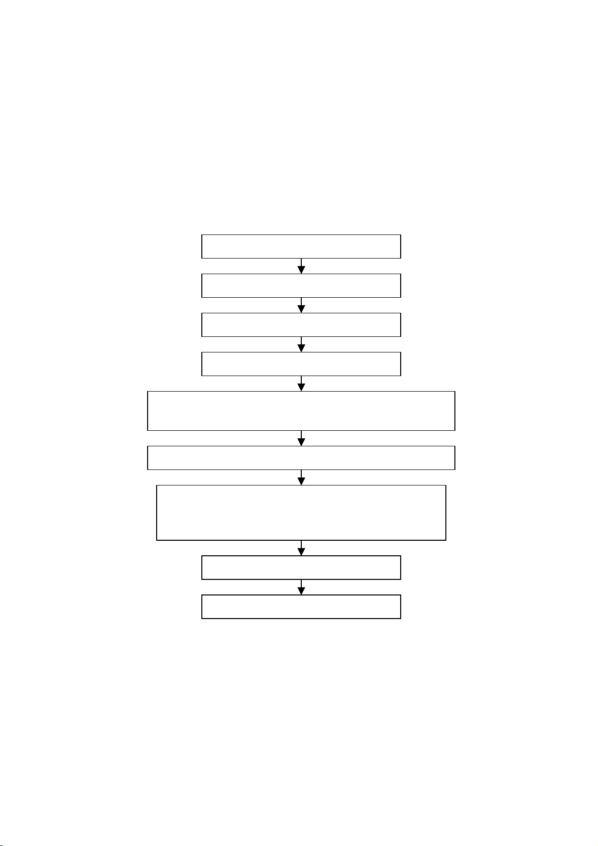
2 Alignment flow-chart
The alignment flow-chart is shown as fig-1
Check MEGA8, DDC and FLASH
To produce digital board and HF board
Check the digital board and HF board
Connect with central signal source, then check each function of TV such as
analog control etc., check the output of headphone and speaker
Input AV/S, HDMI and HD signal, then check each function of all the terminals
Input VGA signal (one format), check if the displ ay is normal under PC
condition, check each function such as analog control etc. , check ho rizo ntal
/vertical center etc.
Check the accessories and pack t hem in box
Fig-1 adjustment flow-chart
3 Unit adjustments
3.1 HF board adjustment
Adjust the Potentiometer VR9002 on the power board, measure the test point TP1 (12VAMP) on
the HF board to be 14 V±0.05 V.
3.2 Digital board adjustment
3.2.1 Connect digital board, button board and HF board, turn on the unit, check if display normal.
3.2.2 Enter factory menu mode (service mode)
Press the MENU button, press the number button: 1 → 9 → 7 → 9, enter factory menu, then use
VOL+/- select item value and CH+/- change it. Press the MENU button exit the factory menu.
All testing
Preset ex-factory
4
Page 7

3.2.3 VGA channel adjustment
3.2.3.1 VGA channel mode preset
Input VGA signal of K-7253, select 640*480/75Hz/85Hz, 1024*768/70Hz/75Hz/80/Hz/85Hz,
800*600/75Hz/85Hz, 1280*1024/60Hz/75Hz and 1600*1200/60Hz respectively, press “AUTO” to do
the auto adjustment until the screen is filled with picture.
3.2.3.2 ADC adjustment of VGA channel
Input the signal of 16 grades of grey density to VG-849 TIME921, PATTERN889, enter factory
menu, select ADC auto correction.
3.2.3.3 White balance adjustment of VGA channel
a. Input K-7253 8 level gray-scale signal of TIME303 (640*480/60Hz/) and PATTERN4718, enter
white balance adjustment menu; adjust the third and seventh levels using white balancer.
b. Select 9300k of “mode”, fixed offset_R to 128, adjust offset_G and offset_B, let the color
coordinate of the third level be 285 and 290 and its brightness be 4.5-5nit. Fixed gain_B to 128,
Adjust gain_R and gain_G, let the color coordinate of seventh level be 285 and 290. Adjust offset_G
and offset_B and gain_R and gain_G repeatedly until the value of the two levels gray-scale to 285
and 290.
c. Select 12000k of “mode”, fixed offset_R to 128, adjust offset_G and offset_B, let the color
coordinate of the third level be 270 and 283 and its brightness be 4.5-5nit. Fixed gain_B to 128,
Adjust gain_R and gain_G, let the color coordinate of seventh level be 270 and 283. Adjust offset_G
and offset_B and gain_R and gain_G repeatedly until the value of the two levels gray-scale to 270
and 283.
Note: after white balance adjustment, adjust 3.2.3.2 item, ADC auto correction again.
3.2.4 AV/TV channel adjustment
3.2.4.1 sub-brightness and sub-contrast adjustment
Input the AV color bar signal (PM5518 COLOUR BAR 100%) to VIDEO terminal, adjust the
sub-brightness and sub-contrast items of the factory menu, exit the factory menu and observe the
effect, repeat the adjustment until it become best.
3.2.4.2 white balance adjustment of AV/TV channel
a. Input AV signal (PM5518, 8 level gray-scale signal), enter white balance adjustment menu; adjust
the third and seventh levels using white balancer.
b. Select 9300k of “mode”, fixed offset_R to 128, adjust offset_G and offset_B, let the color
coordinate of the third level be 285 and 290 and its brightness be 4.5-5nit. Fixed gain_B to 128,
Adjust gain_R and gain_G, let the color coordinate of seventh level be 285 and 290. Adjust offset_G
and offset_B and gain_R and gain_G repeatedly until the value of the two levels gray-scale to 285
and 290.
c. Select 12000k of “mode”, fixed offset_R to 128, adjust offset_G and offset_B, let the color
coordinate of the third level be 270 and 283 and its brightness be 4.5-5nit. Fixed gain_B to 128,
Adjust gain_R and gain_G, let the color coordinate of seventh level be 270 and 283. Adjust offset_G
and offset_B and gain_R and gain_G repeatedly until the value of the two levels gray-scale to 270
and 283.
3.2.5 White balance adjustment of YPbPr channel
a. ADC adjustment of YPbPr channel: input the VG-849 TIME976 and PATTEN984 SMPTE Color
Bar signal, enter factory menu, ADC auto correction.
b. Connect YPbPr signal of K-7253 signal to YPbPr terminal, Input 8 level gray-scale of TIME380
(480i) PATTERN471 signal, enter white balance adjustment menu; Select 9300k of “mode”, fixed
5
Page 8

offset_R to 128, adjust offset_G and offset_B, let the color coordinate of the third level be 285 and
290 and its brightness be 4.5-5nit. Fixed gain_B to 128, Adjust gain_R and gain_G, let the color
coordinate of seventh level be 285 and 290. Adjust offset_G and offset_B and gain_R and gain_G
repeatedly until the value of the two levels gray-scale to 285 and 290.
c. Select 12000k of “mode”, fixed offset_R to 128, adjust offset_G and offset_B, let the color
coordinate of the third level be 270 and 283 and its brightness be 4.5-5nit. Fixed gain_B to 128,
Adjust gain_R and gain_G, let the color coordinate of seventh level be 270 and 283. Adjust offset_G
and offset_B and gain_R and gain_G repeatedly until the value of the two levels gray-scale to 270
and 283.
d. Input 8 level gray-scale signal of TIME392 (480p), TIME394 (720p) and TIME396 (1080i) mode,
repeatedly it until the second color coordinate to 285 and 290 and brightness to 2.3nit.
3.2.6 white balance adjustment of HDMI channel
Input VG-849 (1080i) and 720p HDMI signal, Select 9300k of “mode”, fixed offset_R to 128, adjust
offset_G and offset_B, let the color coordinate of the third level be 285 and 290 and its brightness
be 4.5-5nit. Fixed gain_B to 128, Adjust gain_R and gain_G, let the color coordinate of seventh level
be 285 and 290. Adjust offset_G and offset_B and gain_R and gain_G repeatedly until the value of
the two levels gray-scale to 285 and 290.
Select 12000k of “mode”, fixed offset_R to 128, adjust offset_G and offset_B, let the color
coordinate of the third level be 270 and 283 and its brightness be 4.5-5nit. Fixed gain_B to 128,
Adjust gain_R and gain_G, let the color coordinate of seventh level be 270 and 283. Adjust offset_G
and offset_B and gain_R and gain_G repeatedly until the value of the two levels gray-scale to 270
and 283.
3.3 Performance check
3.3.1 TV function
Enter searching menu → auto search, connect RF-TV terminal with central signal source and check
if there are channels be skipped
3.3.2 AV/S, YPbPr and HDMI terminals
Input AV/S, HD and HDMI signal, check if it is normal.
3.3.3 VGA terminal
Connect to VGA terminal, input VGA format signal of 640 X 480@60 Hz, check if the display is
normal. If the picture still interference, please auto adjustment the picture until it is normal.
3.3.4 DVI terminal
Insert DVI terminal, input signal of 640 X 480@60 Hz signal and check if the display is normal.
3.3.5 Check sound channel
Check the speaker and headphone of each channel.
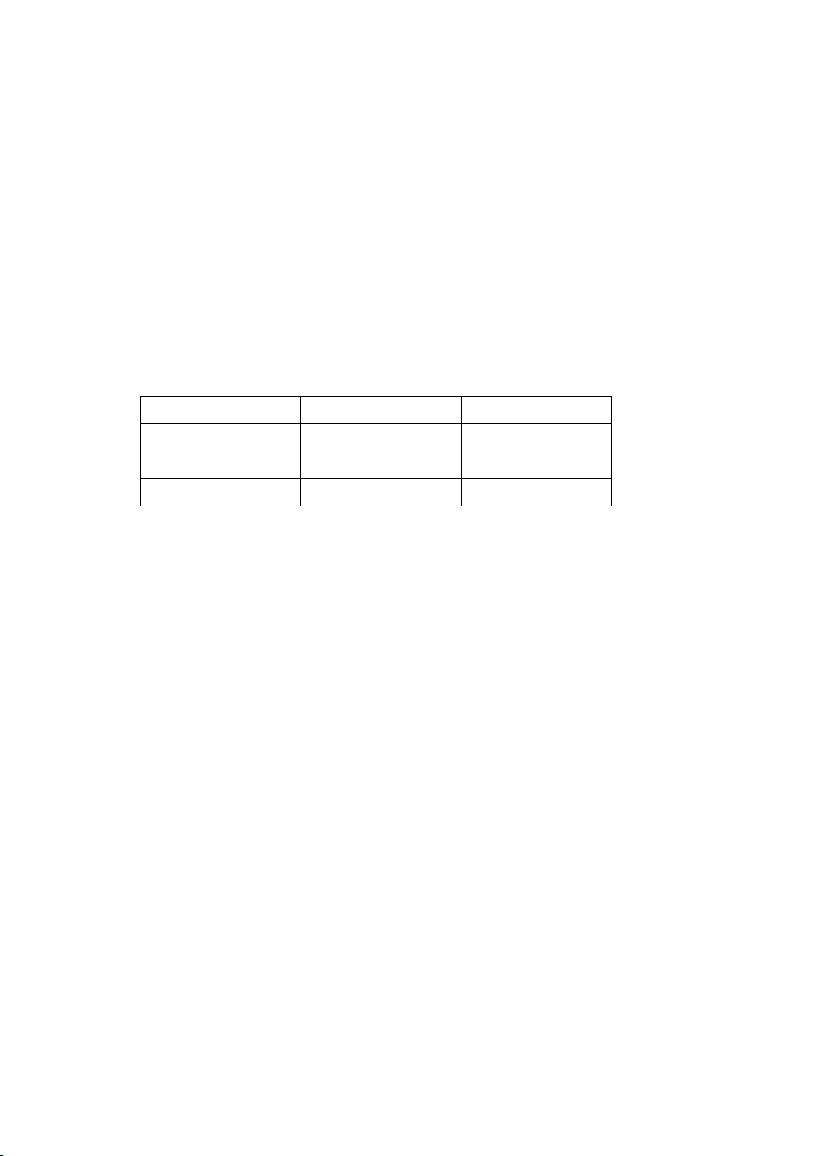
3.3.6 presetting before ex-factory
Item Setting Item Setting Item Setting
Picture mode Sport OSD language English BALANCE +00
Sound mode NEWS VGA color
temperature
Warm Turn on
mode
Off
SCREEN Fill all
6
Page 9
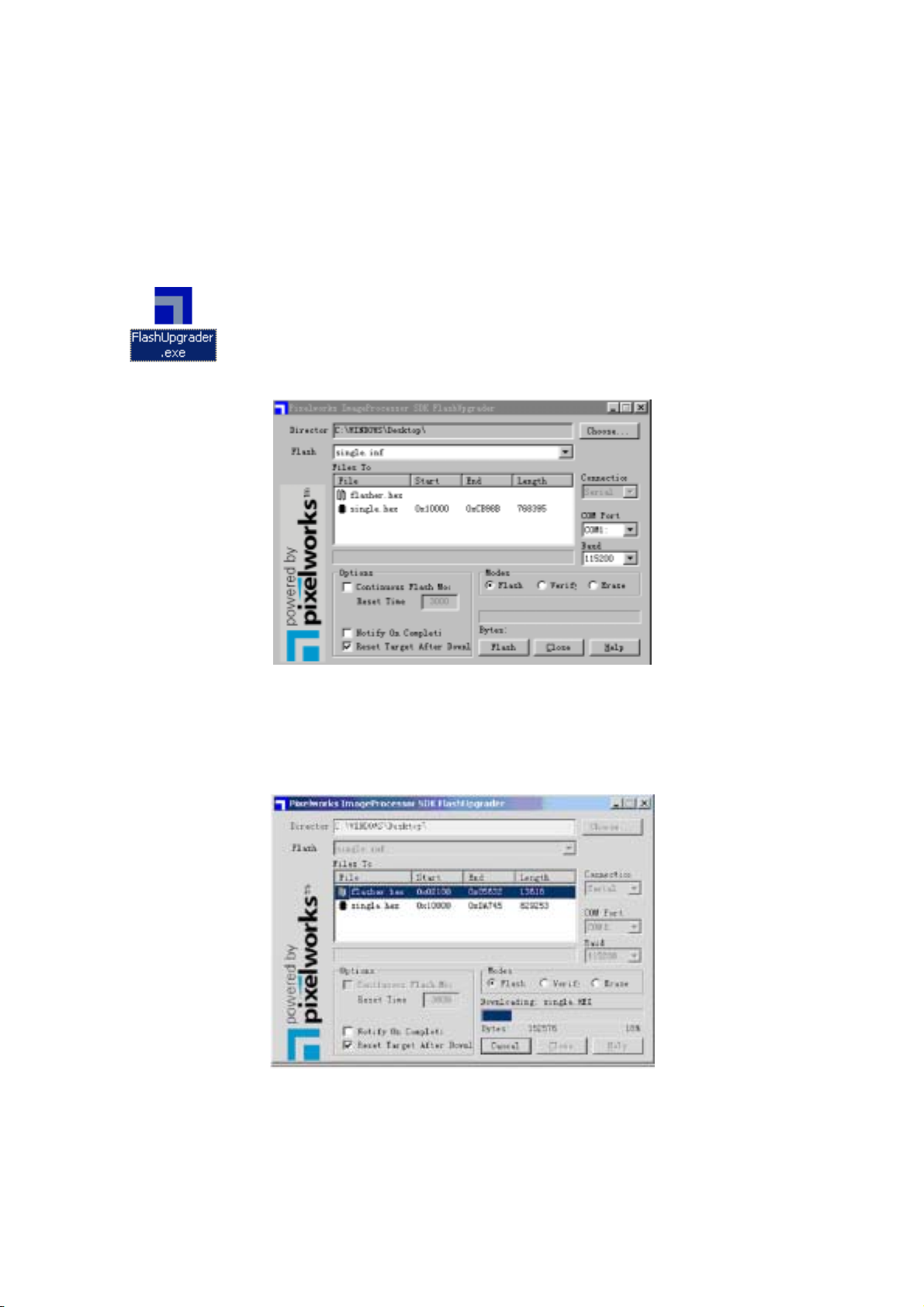
Method of software upgrading
Steps of software upgrading are as follows:
1. Select a serial connection wire and a VGA connection wire and then connect them by means of a
patch panel;
2. Use a serial wire to connect the PC to the patch panel and set TV set to off state;
Open the software upgrade file holder and double click FlashUpgrader (window 2000/XP/NT)
The following interfaces will show up after running the program:
Based on the computer features, set up the serial port (COM Port). Select corresponding serial port
(if it’s unable to FLASH WRITE, change to another port). Baud is selected to be 115200. Then
select Reset Target After Download. Click FLASH pushbutton, it’s ready to run. For other settings,
please refer to the Fig. Above (already defaulted by the system, normally no need to change).
Switch on TV set the FLASH write program begins to run;
After FLASH write is over, push button “cancel” will become flash. Then shut the main power supply
and it’s OK just switch it on again.
Note: Do not shut the power off or turn the TV set on during the FLASH write. Otherwise it may lead
to no way for flash to rewrite.
7
Page 10
Block diagram
N
TUNER
AV1 Video
AV2 Video
AV1 Audio
S-Video
YPbPr1/YcbCr1
YPbPr2/YcbCr2
PC
HDMI
AudioRF
LA72700
or SIF
TV audioTV VIDEO
I2C
Audio
M51797
AV Switch
AV2 Audio HD2 Audio
Video
HDMI audio
PC audio
R2S15900
Audio switch and
control
SDRAM
PW2300
ADC+Decord
AD9398
HDMI
HD1 audio
I2C
24bit RGB
24bit RGB
I2C
MP7720 x 2 Class D
JW1109
I2C
Flash MX29LV800
I2C
PW118
MCU and scaler
LVDS
Speaker
Earphone
PDP SCREEN
ATMEGA8L
power control
I2C
I2C
DDR SDRAM(128M)
EM6A9320
8
Page 11

Working principle analysis of the unit
1. TV board part
This set adopt all system for integrative tuner (include high frequency and intermediate frequency
amplification circuit), the antenna receive the signal and send to the tuner, the tuner is controlled
N602 PW118 MCU (by SDA, SCL), and select the appropriate channel, switch the right mode, after
the high frequency amplification and intermediate frequency amplification, output the video and
audio signals.
The audio signal output by the tuner send directly to AV switch (M52797), select this signal and the
audio signal from AV1, AV2, YPbPr, output the audio signal of the selected channel and separate to
two ways; one way after amplifying 6 db is AU OUT; another way send to audio and sound
processor IC N907 R2A15900. In R2S15900, such signal and audio signal of VGA, HDMI, YPbYr1
are selected by MCU, and output the signal by volume and treble-bass control into D type power
amplifier to amplify, finally output to sound box and represent the sound. When insert the earphone,
the jack of the earphone with the switch send the left/right track of the output of R2S15990 to the
earphone power amplifier N908 NJW1109, after amplifying, when use the earphone output to the
earphone jack to listen (the earphone can select by the customer’s request).
The sound power amplifier MPS7720 is the high effective D type of power amplifier of the single
track. The output power can reach 20W without radiating fin, provided with the protective function of
overcurrent and overheat, when the direct-to-ground input is shorting, it can protect automatically
and stop outputting. If it has been not shorting, it can resume normal circumstance. Therefore,
when plug and play the audio cable (do not suggest such operation), if the set have no sound
because of incautious shorting, it will get right as long as you restart it.
2.The picture part
The video signal outputted by the tuner send to AV switch M52797 (N903), input the video signal of
AV1 and AV2 to M52797 (N903), and switch to gain two group of video output. One group output of
video signal sends to the AV-OUT terminal with its sound output and treat them as the AV OUT
output. Another group output of video signal send to PW2300 and make the video decoding, then
the video signal of S-VIDEO, YpbPr1, YpbPr2, VGA send to PW2300 (N700) synchronously. All of
these video signals shall be sent to this chip to make the video decoding or the AD conversion, and
then output the 24bit digital RGB signal and the related sync signal. PW2300 (N700) complete
mostly the function of 3D comb filter, the channel switch, 5 line Y/C separation, the colour decoding,
and so on. 24 bit digital RGB signal and the related sync signal are outputted by PW2300 (N700)
and are inputted to the next step chip PW118 (N602). The HDMI signal is inputted to AD9398 (N208)
to make the decoding, at the same time 24 bit digital signal and the related sync signal are
outputted and sent to PW118 (N602) to make the processing. PW118 is the new high-powered
image manipulation chip of Pixelworks. The 24 bit digital RGB signal and the related sync signal
outputted by AD9398 and PW2300 shall be inputted to this chip to make the image manipulation. In
addition to the function of interlaced to line-by-line, this chip further include the function of image
enhancement, etc.. PW118 can make the format switch for the different format inputted signal
(under the customer’s request select SCALER function), and accord with the format request of the
screen, and output the low-voltage difference signal of digital RGB LVDS, and then send to the
screen and drive the screen. PW118 is the main CPU as well, the procedure store in external flash
MX29LV800 N404. The software update of RS-232 is that update the stored content of the N404 by
PW118.
9
Page 12
3. IC function, the internal block di agram, t he pi n introduction
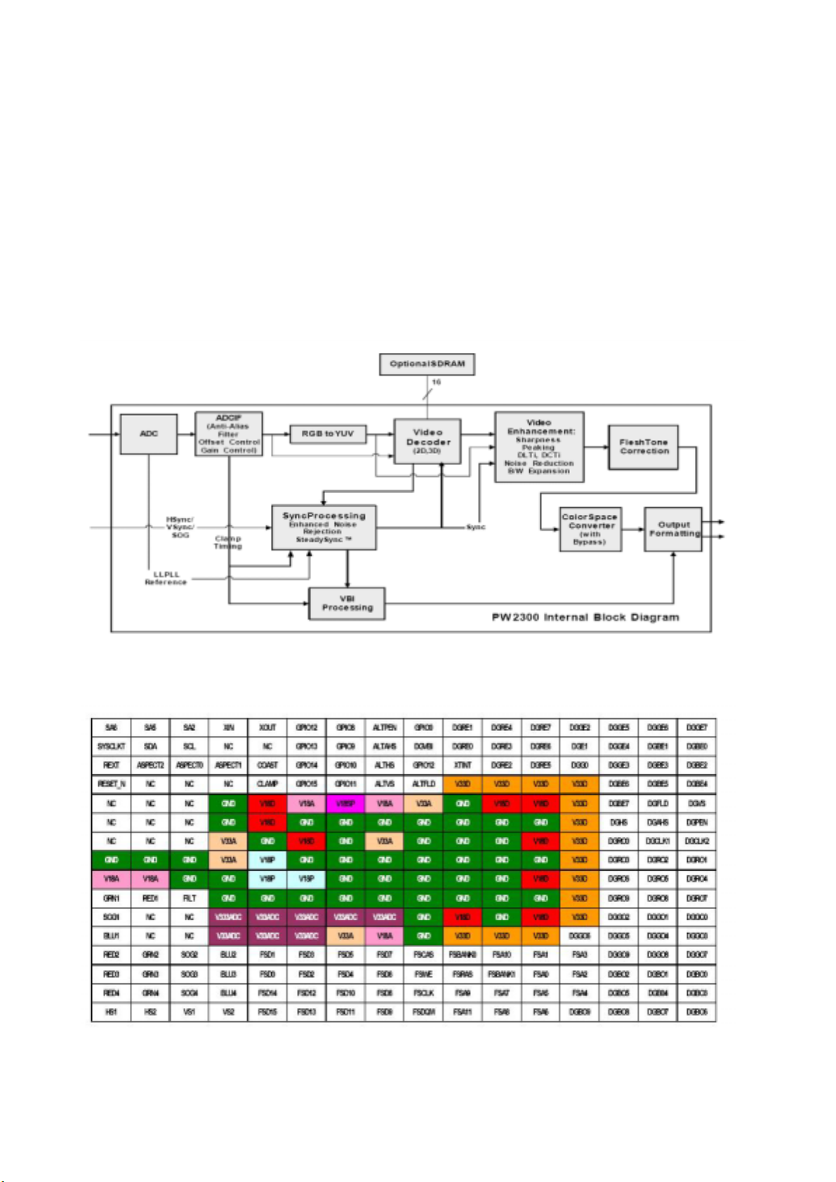
3.1 PW2300
PW2300 is a piece of the front-end video-processing chip that integrates a high-powered,
multi-system video decoder with a high speech ADC module. All of the input video signal (except for
HDMI signal) are inputted to this chip to the AD switch and video decoding, 24 bit digital RGB signal
and the related sync signal are outputted to N602 PW118 to make the processing. PW2300
complete mainly the functions of 3D comb filter, the channel switch, 5-line Y/C separation, the color
decoding and so on. It connect external SDRAM chip N703 HY57V161610E treated as the internal
memory to assist the operation of PW2300.
PW2300 internal block diagram:
PW2300 the arrangement diagram of the pins:
10
Page 13
PW2300 instruction of the pin:
Pin Name Function Pin Name Function
A4 XIN Resonator input N4 B_1 AV1 blue input
A5 XOUT Resonator output P1 R_2 AV2 red input
B2 SDA I2C bus data P2 B_2 AV2 green input
B3 SCL I2C bus clock R3 CVBS_SOG1 T multiple green sync output
of video signal
K2 VGA-R1 VGA red R4 C_1 S-VHS color signal input
K1 VGA-G1 VGA green B9 GVBI Vertical blanking interval
M1 VGA-B1 VGA blue E16 G_VS Vertical sync output
T1 VGA_H VGA CH1 horizontal
sync
T3 VGA_V VGA CH1 vertical sync F15 G_AHS Crude horizontal sync
N1 R_1 AV1 red input G15 G_DLK Clock output
N1 G_1 AV1 green input B10-B12
P3 SOG_2 AV2 green sync input C13,
P4 G_2 AV2 blue input B15-B16
F14 G_HS Horizontal sync output
GRE (0-7) Red data output
A10-A12
C11-C12
GGE (0-7) Green data output
C14
B13,
B14
A13-A16
Blue data output
C15-C16
E14
GBE (0-7)
3.2 AD9398
The chip of high-definition multimedia interface, AD9398 HDMI (High-D efinition Multimedia
Interface) this interface is the digital interface standard that bring up rapidly. The use of this
interface is the transmission of electronic video signal of standard definition and high definition, and
this interface provide the content protect technology. AD9398 also support HDCP (High bandwidth
Digital Content Protection). AD9398 include a HDMI 1.0 interface module and a HDCP module. The
inputted HDMI signal will be sent to the interface of this chip to make the decoding, simultaneity
24-bit digital RGB signal and the related sync signals are outputted to N602 PW118 to make the
processing. Moreover, HDCP module makes the communication by DDCSDA, DDCSCL and HDMI
signal sources to make the video signal decoding. The chip connect a external memory N207
24LC168SN that store the secret key of decoding required by HDCP, and make the communication
by the pin MCL, MDA of AD9893.
11
Page 14
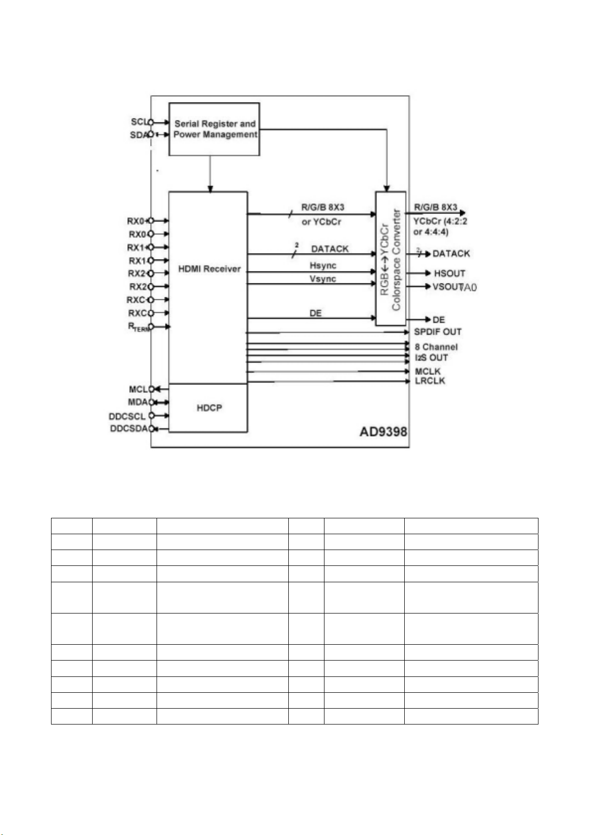
AD9880 (AD9398) internal block diagram:
AD9880 (AD9398) instruction of the pin:
Pin Name Function Pin Name Function
2-9 GGE(0-7) Switch output 44 RXC+ DVI digital video input
12-19 GBE(0-7) Switch output 49 DDC_CLK HDCP (serial data clock)
92-99 GRE(0-7) Switch output 50 DDC_DATA HDCP (serial data I/O)
20, 21 MCLK Control clock output 51 MCL HDCP control series data
clock
22 I2S_SCK Audio series clock output 52 MDA HDCP control series data
I/O
23 I2S_WS Bus clock data output 82 SCL-1 Series data clock
27 I2S_SD Bus audio data output 83 SDA_1 Series data I/O
34 RX0- DVI digital video input 84 G_FIEL0 Parity field output
35 RX0+ DVI digital video input 85 G_VS Vertical data sync output
37 RX1- DVI digital video input 86 G_VHS Green sync output
12
Page 15

The arrangement diagram of the pins:
3.3 PW118
PW118 is the new high-powered image manipulation chip of Pixelworks. The 24 bit digital RGB
signal and the related sync signal outputted by AD9398 and PW2300 shall be inputted to this chip to
make the image manipulation, and are outputted LVDS signal to drive the screen directly. In
addition to the function of interlaced to line-by-line, this chip further include the function of image
enhancement, etc. This chip is the main CPU of this set. It take charge of all control except for the
power supply control, including the control of each chip operation in the main board (eg. the image
manipulation, the channel switch, the image display, etc.), the control of the button, remote device
and sound, etc., and the assistant CPU N401 ATMEGA8L control mainly the power supply,
including the stand-by and the control button of remote device to turn on the set, etc. The menu
interface also generate by PW118. The external memory of PW118 N402 AT24LC32A stores the
related data. The Flash chip N404 MX29LV800 store the related procedure, the chip DDRSDRAM
(N501 K4D553238F-JC) assists the operation of PW118 as the external memory.
13
Page 16

PW118 internal block diagram:
The arrangement diagram of the pins:
3.4 M52797
M52797 is a AV switch chip controlled by IIC. This chip include 4 group of video input and 4 group of
audio input, 2 video output and 1 audio output.
14
Page 17
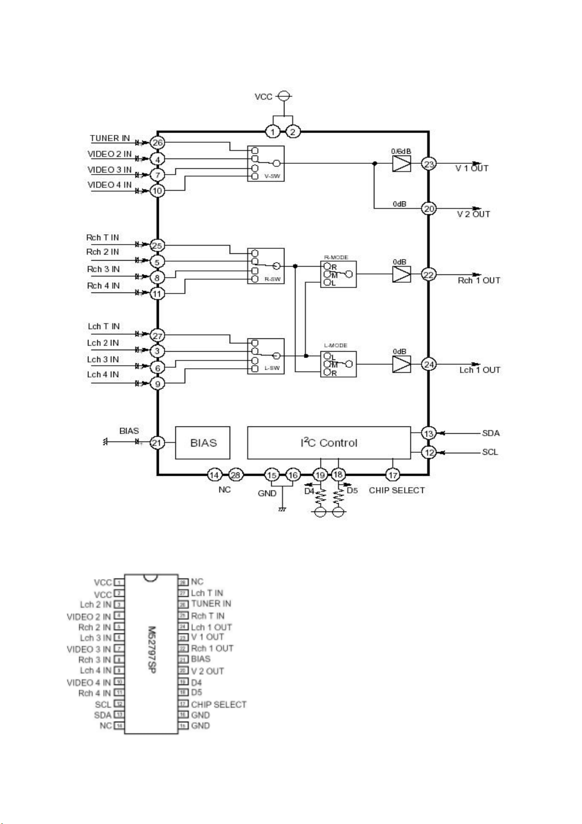
M52797 Internal block diagram:
The arrangement diagram of the pins:
15
Page 18
M52797 instruction of the pin:
Pin Function Pin Function
3 YPbPr2_L audio input 20 Video output to PW2300
5 YPbPr2_R audio input 22 Right track audio output
6 AV1_L audio input 23 Video output to AVOUT interface
7 AV1 audio input 24 Left track audio output
8 AV1_R audio input 25 TV_R audio input
9 AV2_L audio input 26 TV video input
10 AV2 audio input 27 TV_L audio input
11 AV2_R audio input
3.5 R2S15900
R2S15900 is a audio processing chip that take charge of audio switch, sound processing and
volume adjustment, controlled by IIC bus.
Internal block diagram:
16
Page 19
R2S15900 instruction of the pin:
Pin Function Pin Function
2, 27 Left and right track of M52797 5, 24 Left and right track of YPbPr1
3, 26 Left and right track of HDMI 11, 19 Left and right track of audio output
4, 25 Left and right track of VGA
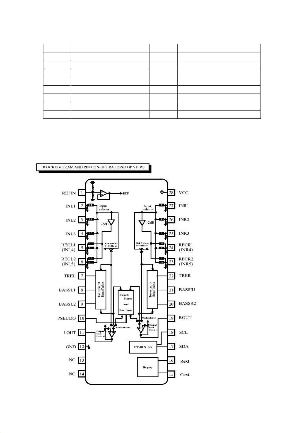
3.6 LA72700 (STEREO/SAP DECO DER) :
PIN description:
Pin No. Name Description Pin No. Name Description
5 PISIF Audio IF input 25 R OUT Right channel audio output
11 SDA I2C bus 26 LOUT Left channel audio output
12 SCL I2C clock 31 VCC 9V
17
Page 20
Diagnose and service of panel
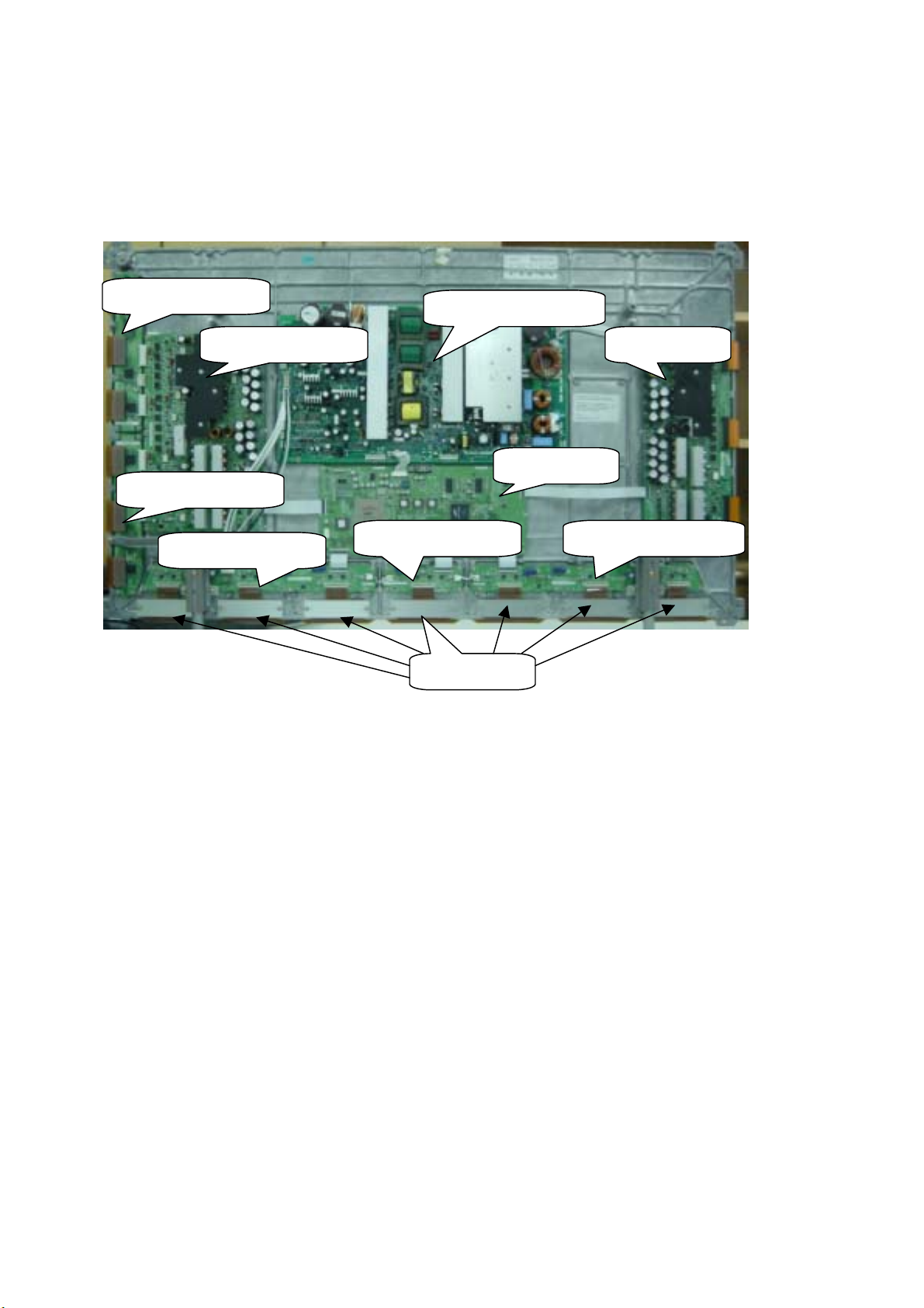
1. Block function of panel
The power supply board, Logic board, X drive board, Y drives board, Logic BUFFER (E, F and G)
and Y BUFFER (upper and lower) of the PDP panel.
Y BUFFER (upper)
Y BUFFER (lower)
Logic BUFFER (E)
Logic BUFFER(F) Logic BUFFER(G)
Power supply board
X drive board Y drive board
Logic board
COF(7 piece)
* Power supply board: to supply power for the screen, other functional modules on the screen, our
own main board, and video frequency processing board.
* X driving board: to produce and provide driving signal for X electrode according to the time
sequence signal sent from logic board.
* Y driving board: to produce and provide driving signal for Y electrode according to the time
sequence signal sent from logic board.
*Logic board: to process the image signal sent from the main board, to produce addressing signal
and to provide driving signal for X and Y driving boards.
*Logic BUFFER board: To convert the data signal and control signal sent from the logic board into
the signals required by COF.
*Y BUFFER board: to transmit the scanning signal from the Y driving board to the screen, which is
divided into upper and lower parts.
*COF: to convert the signal sent from the logic BUFFER board into the address signal used by the
screen.
2.Trouble diagnosis:
2.1 The screen is not bright:
a. Check if the power supply plug from the power filters board to the power supply board is well
inserted into the socket. If not, plug it in.
b. Check if the fuse on the power supply board is blown up. If yes, replace it for a good one.
c. Remove our main board and the video frequency processing board, ground the pin 4
18
Page 21
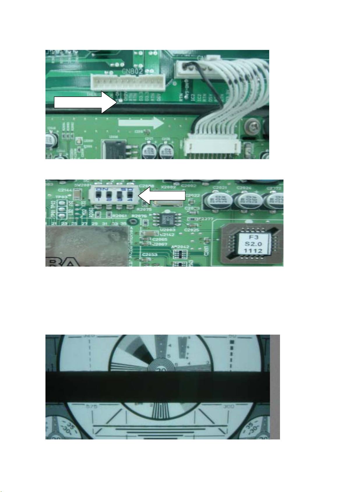
POWER_ON/OFF of socket CN802 of the power supply board;
SW200
Solder point
and then push the slide switch SW2001 on the logic board to the internal modes (1, 3 up and 2, 4
down) from external modes (1, 2, 4 up and 3down).
1
Switch the power on and see if the screen is lit. If the screen can give a normal and completely
white field signal, then the problem lies in our main board or video frequency processing board,
which will be dealt with separately.
d. If the screen is not lit, then first replace the power supply board to see if the problem is solved.
e. If the problem remains after the power supply board is replaced, then the problem lies in the
screen, replace the entire screen for treatment.
2.2 There appears on the screen a line or several unlit lines.
Check if the socket between Y driving board and Y BUFFER is plugged well. If not, plug it well. If
19
Page 22

yes then replace Y BUFFER (upper, lower) in respect to the upper, lower part of the dark line on the
screen.
2.3 There appear on the screen one or several horizontal lines that are much brighter than the
remaining horizontal lines at the edge:
Check if the socket between Y driving board and Y BUFFER is plugged well. If not, plug it well. If
yes then replace Y BUFFER (upper, lower) in respect to the upper, lower part of the dark line on the
screen.
4.There appear on the screen one vertical unlit line or a vertical entirely unlit block
a. If it’s one vertical unlit line, then COF has problem.
b. If it’s a vertical entirely unlit block, then first check if the connection socket between COF and
logic BUFFER has problem. If not, check if the connection sockets between the logic BUFFER and
the logic board is normal. If yes, replace the logic BUFFER. Finally, if the problem still remains when
the replacement is over, then replace the logic board.
5.There appears on the screen a mono color signal and one or several vertical bright lines of other
colors:
a. If it’s a vertical bright line of other colors, then the problem lies with COF or the screen.
b. If it’s an entire vertical block of other colors, then first check to see if the connection socket
between COF and logic BUFFER has problem. If no problem, check if the connection socket
between the logic BUFFER and the logic board is normal. If it’s normal, then replace the logic
BUFFER. If the problem still remains after the replacement, then replace the logic board. Finally if
the problem is still there, then the problem lies with COF.
6.There appear on the screen abnormal bright spots or blocks that are different from what’s
described above:
a. Check if the connection socket between COF and logic BUFFER board has been well plugged.
b. Replace the logic BUFFER board. If it’s not solved then replace logic board. If the problem still
remains, then it’s the problem with COF.
20
Page 23

Wiring Diagram
Logic board
LA03
31 7 11 10 4
`
X600 X400 X405
Panel
Power supply filter board
2
Power supply board
CN9004 CN9003 CN8001
Speaker assembly
X909 X908
button board
Data processing board
RS-232 HDMI VGA
YPbPr/YCbCr1 YPbPr/YCbCr2
21
X301 X300 X302
X904 X903 X906
HF board
6 12 9
AV out
S-Vide o in
AV1 in AV2 in
earphone
RF
Page 24

Main assembly list
The unit No. Part NO. Description
203-PS42T80-18 301-CPS42D8-14C RC-C14-0C Remote Control (LEGEND)
615-10412-0G0 Stand assy
615-20415-0G0 Speaker box assy
667-PSIT6-55A High frequency board assy
667-PSIT6-69 digital board assy
667-PS42T6-05 Button board assy
335-42006-00 Screen
203-PS42T80-19 301-CPS42D8-14B RC-C14-0B Remote Control (PRIMA)
615-10412-0G0 Stand assy
615-20415-02 Speaker box assy
667-PSIT6-55A High frequency board assy
667-PSIT6-69 digital board assy
667-PS42T6-05 Button board assy
335-42006-00 Screen
203-PS42T80-20 301-CPS42D8-14A RC-C14-0A Remote Control (INSIGNIA)
615-10412-02 Stand assy
615-20415-03 Speaker box assy
667-PSIT6-55A High frequency board assy
667-PSIT6-69 digital board assy
667-PS42T6-05 Button board assy
335-42006-00 Screen
22
Page 25

Trouble shooting guide
n
y
b
d
f
p
y
d
y
f
N
N
N
N
N
1.No raster, no picture, no sound
o raster, no picture, no sound.
Measure the level of 8th pin of X405:
when use V4 screen, it should be low
level; when use V7 screen, it shoul
be high level.
ormal
Check the level
of power suppl
pin of each IC.
Check power suppl
D3.3V, D5V
Abnormal
Abnormal
Check N401
NOTICE: The PDP power supply have the protection function of overcurrent, overvoltage
and so on, if certain route power supply appear overcurrent and overvoltage, the power
supply should appear the protection to arise no-output.
Check if the power supply indicator light is on.
yes
ormal
Check if the
union joint o
602 and LVDS
line is loose.
no
Check N401
and keyboard.
Cut off the connectio
between power suppl
oard and data board, an
test 5V-STBY
Abnormal
Check 5V-STBY
ormal
The problem o
ower supplies
board.
23
Page 26

2.With sound but no picture:
p
N
y
d
N
f
p
N
t
N
N
N
N
N
Check if all other channel
has no
and peripher
circuit
icture.
o
602 PW118
Turn to check 4
of program
With sound but no picture.
Display logo?
Yes
Check if the G401 an
Yes
ormal
602 damaged.
G7000 have the signal
wave.
Abnormal
Check the input signal of N602
and
ower supply.
o
ormal
Check N700
and the circui
of output.
Unfix X405 and X406, short
circuit the PIN8 of X405 to G
set switch of the logic board as
self-testing signal, then check i
display the white screen.
ormal Abnormal
The screen damaged.
Abnormal
Set self-testing of the screen:
a. 42” SD screen: Push down 2 and 4 and push up 3 of SW2001 on the logic board;
b. 50” HD screen: Push down 1 and 4 and push up 2, 3, 5, and 6 of SW2001 on the logic board;
c. Please make sure resume it to the original status when the check is over.
D,
24
Page 27

3.With picture but no sound:
r
d
p
r
N
N
N
t
p
N
N
N
N
If the sound power board X908 is output.
Check if the second pin of soun
ower amplifier input the signal.
The sound power amplifier or peripheral
circuit has problem. Check power supply,
if the control of SHUTDOWN pin is
normal; if output short-circuited or othe
problems that cause protection to work.
Check N907 o
peripheral circuits.
4. A certain channel is abnormal
4.1 No picture on AV
Check N602 and
periphery circuit
Check if TV channel is
normal.
Yes
Check if N700
output is normal.
o Yes
The sound damaged.
oYes
Measure if the sound
input of current channel
of N907 is normal.
oYes
Check different levels of
circuit following input audio
signal channel.
Measure if the AV inpu
in of N700 have the
signal input.
oYes
Check N903 M52797
and periphery
o
Yes
o
700 is damaged
25
Page 28

4.2 YPrPb or YCrCb no picture
p
n
d
No N
f
N
N
N
N
N
Check if the YPRYPB input pi
of N700 have signal.
Check N700 an
periphery circuit
4.3 TV no picture
700 damaged
Check if AV channel
is normal.
ormal Abnormal
o Yes
Check if YPRPB 1 / YCRCB1 a nd YPRPB2
/YCRCB2 channels is no
Yes
Yes
Check if the input signal o
700 is normal.
ormal
Check if N700 has
output.
o
icture.
check interface
circuit.
Abnormal
Check N602 and
periphery circuit
Check N903
M52797 and the
tuner.
26
Page 29

4.4 VGA no picture
d
t
N
N
Check the horizontal and vertical sync
signal of HS1 and VS1 input of N700.
ormal
Check N700 an
periphery circuit
Check if the input YPRPB
signal is normal.
o Yes
Check N700 and
periphery circuit
Abnormal
The matter of inpu
interface circuit, N211
and periphery circuit
4.5 HDMI no picture
If no picture, check firstly if the set of external device is normal, after eliminating the device problem
still no picture, check X200, N208 and periphery circuit.
4.5.1 Abnormal of the picture:
a. A certain differential wire pair of LVDS (RX0+/-, RX1+/-, RX2+/-, RX3+/-) of X600 is abnormal,
which may lead to lack of color (it’s not a complete loss of color).
b. Failure with resistor rows R606~R610, which may lead to loss of corresponding color from the
gray degree corresponding to the picture of all channels.
c. Failure with resistor rows R708~R713, which may lead to loss of corresponding color from the
gray degree corresponding to the picture of VGA/YPRPB/AV/TV channels.
d. Failure with resistor rows R258~R263, which may lead to loss of corresponding color from the
gray degree corresponding to the picture of HDMI channel.
4.5.2 Abnormal picture vertically or horizontally (bar like): Abnormal in complete line extending all
the way from up downward on the screen of stand definition TV set; abnormal vertically on half
screen of high definition TV set. They may be caused by the damage of the address BUFFER
module that directly corresponds to its position, or may be caused by the damage of the connection
wire that directly corresponds to the position of the screen. The horizontal bar like abnormality is
also related to the Y driving circuit that corresponds directly to its position. To judge these
phenomena, It’s possible to check it by setting the screen to the status of self check as explained
above
4.5.3 No brightness in the square block area: Normally it’s caused by the damage of the address
BUFFER module that directly corresponds to its position, or may be caused by the damage of the
connection wire that directly corresponds to the position of the screen. To judge these phenomena,
it’s possible to check it by setting the screen to the state of self-check as explained above.
27
Page 30

Schematic diagram(602-PS42T8-23)
Digital Board
Page 1 of 10
Page 31

Digital Board
Page 2 of 10
Page 32

Digital Board
Page 3 of 10
Page 33

Digital Board
Page 4 of 10
Page 34

Digital Board
Page 5 of 10
Page 35

Digital Board
Page 6 of 10
Page 36

Digital Board
Page 7 of 10
Page 37

Digital Board
Page 8 of 10
Page 38

Analog Board
Page 9 of 10
Page 39

Key Board
Page 10 of 10
Page 40

EXPLODED VIEW
Page 41

PART LIST OF EXPLODED VIEW
NO. DESCRIPTION PART#
1 Speaker cover 808-10622-G0
2 Speaker front cover 780-3A133-120
3 Speaker 384-41504-50
4 Speaker back cover 780-30134-AF0
5 Sound box fixed board 804-20337-AF0
7 Middle cabinet 780-I08R1JAF0
8 LED column 700-60186-00A
9 Button board assy 667-PS42T6-05
10 Button 877-60593-G0
11 Filter glass 740-10138-00
12 Hold down board 803-30145-00
13 Hold down board 803-30144-00
14 Trans-connecting support 870-10310-00 /870-10311-00
15 Panel 335-42006-00
16 CPU assy 667-PSIT6-69
17
18
19 Back cabinet 611-I08RR-AF3A
20 Socket 364-49213-00
21 Screw 851-24016-14
22 Socket 364-44206-00
23 Rear panel 804-2H389-AF0
24
25 Stand 807-20217-0G0
Page 42

PART LIST
PART# DESCRIPTION LOCA.NO.
100-PS42T80-19 PS-42T8
100-PS42T80-05 PS-42T8 10Z
335-42006-00 DISPLAY SCREEN PDP42V7 !
364-41207-00 ANTENNA SOCKET HR-F
364-44206-00 SOCKET WP4-7
485-10144-00 POWER CORD LAP-31+LAS-13 !
488-10012-00 BATTERY 7#( made in china
604-PS42T87-01 OWNER'S MANUAL(PRIMA CAN/RC-C)
611-I08RR-AF3A BACK CABINET ASS'Y ( GREY 05,SILK-SCREEN
644-10184-05 IMITATEUL1015 18# 100mm YELLOW /GREEN
655-33101-43 (3-PINS) LEAD WITH HOUSING
655-4E302-116 (4-PINS) LEAD WITH HOUSING
665-D0002-421 VIDEO LINE BLUE GREEN RED
665-D0002-422 VIDEO LINE YELLOW WHITE RED
665-D0002-423 AUDIO LINE XH-3.5-RCA-2000
665-D0002-438 SOUND LINE 2M
665-D0002-581 *LVDS LINE 30-PINS 220mm
700-60186-00A LED COLUMN
740-10138-00 FILTER GLASS K0R-XCC-02 (S1)
741-10001-02 WIRE FIXED BLADE
741-10001-02 WIRE FIXED BLADE
742-30032-00 TIE
742-30032-00 TIE
780-I08R1JAF0 MIDDLE CABINET (ABS V0 GREY 05 )
780-I08R2JAR2A FRONT CABINET ( ABS V0 BLACK ,SILK-SCREEN )
803-30144-00 PRESS BOARD (TOP )
803-30145-00 PRESS BOARD (BOTTOM )
803-30146-00 PRESS BOARD ( LEFT )
803-30147-00 PRESS BOARD ( RIGHT )
804-20337-AF0 SOUND BOX FIXER( GREY 05)
804-2H389-AF0 BLACK PLATE
808-70245-00 INSULATING CUSHION(230X200)
808-70337-00 EVA GLUE (942X5X7.5 SOFT)
808-70337-00 EVA GLUE (942X5X7.5 SOFT)
808-70338-00 EVA GLUE (550X5X7.5 SOFT)
808-70338-00 EVA GLUE (550X5X7.5 SOFT)
808-80222-01 ELECTRIC GASKET (8X2X1035) ALUMINIUM FOIL
808-80222-01 ELECTRIC GASKET (8X2X1035) ALUMINIUM FOIL
808-80223-01 ELECTRIC GASKET (8X2X344) ALUMINIUM FOIL
808-80223-01 ELECTRIC GASKET (8X2X344) ALUMINIUM FOIL
808-80224-01 ELECTRIC GASKET (8X2X74) ALUMINIUM FOIL
808-80224-01 ELECTRIC GASKET (8X2X74) ALUMINIUM FOIL
808-80225-01 ELECTRIC GASKET (8X2X160) ALUMINIUM FOIL
808-80225-01 ELECTRIC GASKET (8X2X160) ALUMINIUM FOIL
Page 43

808-80228-01 ELECTRIC GASKET (8X2X685) ALUMINIUM FOIL
808-80240-01 ELECTRIC GASKET (20X12X70) ALUMINIUM FOIL
808-80241-01 ELECTRIC GASKET (8X4.5X100) ALUMINIUM FOIL
808-80241-01 ELECTRIC GASKET (8X4.5X100) ALUMINIUM FOIL
808-80248-01
808-80248-01
ELECTRIC GASKET (8X2X974) ALUMINIUM FOIL
ELECTRIC GASKET (8X2X974) ALUMINIUM FOIL
808-80249-01 ELECTRIC GASKET (8X2X549) ALUMINIUM FOIL
808-80249-01 ELECTRIC GASKET (8X2X549) ALUMINIUM FOIL
851-23008-11 SCREW SJ2824 ST3X8C-D.Zn
851-23008-11 SCREW SJ2824 ST3X8C-D.Zn
851-23008-11 SCREW SJ2824 ST3X8C-D.Zn
851-23008-11 SCREW SJ2824 ST3X8C-D.Zn
851-23010-31 SCREW SJ2824 ST3X10FT-D.Zn
851-23010-31 SCREW SJ2824 ST3X10FT-D.Zn
851-23010-31 SCREW SJ2824 ST3X10FT-D.Zn
851-23010-31 SCREW SJ2824 ST3X10FT-D.Zn
851-24014-34 SCREW SJ2824 ST4X14FT-Y
851-24014-34 SCREW SJ2824 ST4X14FT-Y
851-24016-14 SCREW SJ2824 ST4X16C-Y
851-24016-14 SCREW SJ2824 ST4X16C-Y
851-53010-31 SCREW SJ2825 ST3X10FT-D.Zn
851-53010-31 SCREW SJ2825 ST3X10FT-D.Zn
852-14008-81 SCREW P(+)M4X8-D.Zn
852-14008-81 SCREW P(+)M4X8-D.Zn
852-18010-84 SCREW P(+)M8X10-Y
852-18010-84 SCREW P(+)M8X10-Y
852-23008-81 SCREW SJ2829 M3X8-D.Zn
852-23008-81 SCREW SJ2829 M3X8-D.Zn
852-23008-81 SCREW SJ2829 M3X8-D.Zn
852-24006-81 SCREW SJ2829 M4X6-D.Zn
852-43010-84 SCREW F(+) M3X10-Y
852-43010-84 SCREW F(+) M3X10-Y
852-54008-84 SCREW SJ2830 M4X8-Y
852-54008-84 SCREW SJ2830 M4X8-Y
852-54018-84 SCREW SJ2830 M4X18-Y
852-54018-84 SCREW SJ2830 M4X18-Y
852-84010-81 COMPOSE SCREW SJ2835 M4X10-DZn
852-84010-81 COMPOSE SCREW SJ2835 M4X10-DZn
852-93006-81 COMPOSE SCREW SJ2836 M3X6-D.Zn
852-93006-81 COMPOSE SCREW SJ2836 M3X6-D.Zn
855-A0058-00 SCREW M3X19.5
855-A0058-00 SCREW M3X19.5
862-20039-00 CARTON CLIPS
863-80969-00 POLY FOAM (TOP LEFT )
863-80970-00 POLY FOAM (TOP RIGHT )
863-81302-00 POLY FOAM ( LEFT BOTTOM EPE)
Page 44

863-81303-00 POLY FOAM ( RIGHT BOTTOM EPE)
863-81304-00 CUSHION (EPE)
868-20037-02 FIBRE WASHER φ8Xφ3.2X0.8RED
868-20770-00 INLAY M3X9
868-20770-00 INLAY M3X9
868-20771-00 RUBBER WASHER φ11Xφ5X3.5
868-20771-00 RUBBER WASHER φ11Xφ5X3.5
870-10192-00 BRACKET ( LEFT )
870-10193-00 BRACKET ( RIGHT )
870-10310-00 TRANS-CONNECTING BRACKET ( LEFT )
870-10311-00 TRANS-CONNECTING BRACKET ( RIGHT )
870-3A121-00 EAR BRACKET ( LEFT TOP RIGHT BOTTOM )
870-3A122-00 EAR BRACKET ( RIGHT TOP LEFT BOTTOM )
877-60593-AR0 BUTTON ( BLACK )
880-10628-B1
FRONT LOGO (NEW PRIMA SILVERY BLACK BOTTOM42")
881-60085 BLANK WARNING LABEL
881-61884-00 CSA WARNING LABEL
881-62884-174 BACK PLATE LABEL (PS-42T8,PRIMA)
881-63016-00A POWER SYMBOL LABEL ( T2751)
881-63057-00 WARNING LABEL
881-63071-00 GROUNDING LABEL
881-63516-00 LABEL (PS-42D8 G,LG PANEL )
881-80675-00
SERVICE CARD ( LCD37以TOP )
881-PS42T87-00 OPERATION CARD ( HOLDER )
886-31417-02 ACCESSORY PACKING BOX ( ENGLISH )
886-31565-00 CARTON BOX BOTTOM COVER
886-31864-15A CARTON BOX (PS-42T8,PRIMA)
886-31866-00 CUSHION
887-20198-00 PALSTIC BAG 90X280X0.04
887-21135-03 CLASPER PALSTIC BAG 230X330X0.1
887-21207-P3 PE/PEARL COTTONPALSTIC BAG 1500X1000 ENGLISH
615-10412-0G0 PANEL HOLDER ASS'Y ( SILVER WHITE 06)
807-20217-0G0 HOLDER ( SILVER WHITE 06)
808-20307-01 PMMA PANEL (SILK-SCREEN )
820-20039-00 BALANCE BOARD
851-43008-32 SCREW F(+)T3X8BT-D.Ni
851-43008-32 SCREW F(+)T3X8BT-D.Ni
852-44008-82 SCREW F(+)M4X8-D.Ni
852-44008-82 SCREW F(+)M4X8-D.Ni
852-44008-82 SCREW F(+)M4X8-D.Ni
852-44008-82 SCREW F(+)M4X8-D.Ni
868-20478-00A CUSHION
870-40194-0Z0 STAND COLUMN ( LEFT ) , TRANSPARENT
870-40195-0Z0 STAND COLUMN ( RIGHT ), TRANSPARENT
Page 45

887-21198-00 PEARL COTTON PLASTIC PAPER(1200X700X0.5)
615-20415-02 SOUND BOX ASS'Y (LG BLACK / GREY 05)
808-10622-AR0 SOUND BOX COVER ( BLACK )
364-42201-00 SOCKET WP2-9C
384-41504-50 SPEAKER YDT813-14P
770-25112-72 RV105 12X0.15 250mm RED
770-25112-76 RV105 12X0.15 250mm BLUE
780-3A133-120 SOUND BOX FRONT CABINET ( MOLD GREY G05)
780-30134-AF0 SOUND BOX BACK CABINET ( GREY 05)
808-70259-00 EVA GLUE (25X15X2)
822-10192-00 BUSH
851-23012-14 SCREW SJ2824 ST3X12C-Y
851-23012-14 SCREW SJ2824 ST3X12C-Y
851-24012-11 SCREW SJ2824 ST4X12C-D.Zn
851-24012-11 SCREW SJ2824 ST4X12C-D.Zn
851-24016-11 SCREW SJ2824 ST4X16C-DZn
851-24016-11 SCREW SJ2824 ST4X16C-DZn
864-10178-AR0 SPEAKER NET ( BLACK )
864-90044-00 SOUND ABSORBENT
868-20707-00 SEALING PIECE ( EVA 740X5X1.5)
868-20707-00 SEALING PIECE ( EVA 740X5X1.5)
868-20709-00 SEALING PIECE ( EVA 150X2.8X1)
868-20709-00 SEALING PIECE ( EVA 150X2.8X1)
868-20720-00 SEALING PIECE ( 400X2.8X2.8)
KEY1 HDCP
SPS42T60-01B10 SOFTWARE MEGA8 N401
SPS42T60-01C10 SOFTWARE HDMI EDID N200
SPS42T60-01D10 SOFTWARE VGA EDID N205
667-PSIT6-69 DSP BOARD ASS'Y
667-PSIT6-69\ DSP BOARD ASS'Y (MANUAL INSERTION )
855-A0053 HEXAGONAL SCREW M3X7
855-A0068 HEXAGONAL SCREW M3X4.5
329-33204-00 CRYSTAL 32.768K G400
329-61402-00 CRYSTAL HC-49/US 14.31818MHZ G401
329-62706-00 CRYSTAL HC-49US 27MHZ G700
364-11212-00 EARPHONE JACK ST-112 X100
364-11212-00 EARPHONE JACK ST-112 X101
364-11212-00 EARPHONE JACK ST-112 X202
364-351BD-00 5-PINS CONNECTORS 53047-0510 X403
364-361AY-00 6-PINS CONNECTORS TJC10-06A X302
364-37101-00 7-PINS CONNECTORS TJC3-07A X400
364-3B1AY-00 12-PINS CONNECTORS TJC10-12A X300
364-49213-00
SOCKET RS232 阳
X401
Page 46

364-91227-00 VGA SOCKET SCREW X201
364-93220-00 AV JACK AV3-14WD X102
364-93220-00 AV JACK AV3-14WD X103
364-391AY-00 9-PINS CONNECTORS TJC10-9A X301
464-6C747-M0 ELECTROLYTIC CAPACITOR CD110-10V-470uF-M C430
464-6C810-M0 ELECTROLYTIC CAPACITOR CD110-10V-1000uF-M C440
464-6D810-M0 ELECTROLYTIC CAPACITOR CD110-16V-1000uF-M C437
364-35101-00 5-PINS CONNECTORS TJC3-05A X203
655-6E301-54 (6-PINS) LEAD WITH HOUSING
655-9E301-18 (9-PINS) LEAD WITH HOUSING
655-B4301-14 (12-PINS) LEAD WITH HOUSING
655-91201-101 (9-PINS) LEAD WITH HOUSING
655-71201-88 ( 7-PINS ) LEAD WITH HOUSING
666-13001-00 FERRITE BEAD TY30X20X10
667-PSIT6-69* DSP BOARD ASS'Y (SMD )
340-00001-0S SMD DIODE LL4148 D404
340-00001-0S SMD DIODE LL4148 D405
340-00296-00 SMD DIODE SK34 D403
340-00372-00 SMD DIODE MMBD1204 D200
340-00372-00 SMD DIODE MMBD1204 D201
342-01380-00 *SMD TRANSISTOR BSS138LT1 V207
342-01380-00 *SMD TRANSISTOR BSS138LT1 V208
342-01380-00 *SMD TRANSISTOR BSS138LT1 V400
342-01380-00 *SMD TRANSISTOR BSS138LT1 V401
342-01380-00 *SMD TRANSISTOR BSS138LT1 V402
342-08470-90 SMD TRANSISTOR BC847AW V105
342-08470-90 SMD TRANSISTOR BC847AW V106
342-08470-90 SMD TRANSISTOR BC847AW V107
342-08470-90 SMD TRANSISTOR BC847AW V109
342-08470-90 SMD TRANSISTOR BC847AW V110
342-08470-90 SMD TRANSISTOR BC847AW V111
342-08470-90 SMD TRANSISTOR BC847AW V204
342-08470-90 SMD TRANSISTOR BC847AW V205
342-08470-90 SMD TRANSISTOR BC847AW V206
342-08470-90 SMD TRANSISTOR BC847AW V403
342-08470-90 SMD TRANSISTOR BC847AW V404
353.01180-20 *SMD ICPW118B-10L N602
353-00080-90 SMD ICATMEGA8L-8AI N401
353-05040-20 SMD IC PESD5V0L4UG N100
353-05040-20 SMD IC PESD5V0L4UG N101
353-05050-20 SMD IC PESD5V0L5UY N102
353-05050-20 SMD IC PESD5V0L5UY N103
353-05050-20 SMD IC PESD5V0L5UY N214
353-11170-10 SMD IC B1117N-2.5 (D) N301
353-11170-10 SMD IC B1117N-2.5 (D) N500
Page 47

353-11170-G0 SMD IC AMS1117-1.8 (D) N209
353-11170-G0 SMD IC AMS1117-1.8 (D) N302
353-11170-G0 SMD IC AMS1117-1.8 (D) N801
353-12130-10 SMD ICCM1213-08MS N212
353-12130-10 SMD ICCM1213-08MS N213
353-15010-30 SMD ICAP1501-33K5 N405
353-16161-70 SMD IC M12L1616A-7T (D) N703
353-17420-00 SMD IC PCM1742E N210
353-20090-10 SMD ICCM2009-00QS N211
353-23000-50 SMD ICPW2300-05 N700
353-24160-60 *SMD IC 24LC16BSN N207
353-24210-50 SMD IC 24LC21A/SN N205
353-24220-10 SMD IC 24LCS22SN N200
353-24640-00 SMD IC24LCSN N402
353-29800-40 SMD IC MBM29LV800TA-90PFTN N404
353-32320-50 SMD IC MAX3232CSE (M) N400
353-93200-10 SMD ICEM6A9320BI-5 N501
353-93980-10 SMD IC AD9398XSTZ-150 N208
364-T1901-00 SMD 19-PINSHDMI1775244-2 X200
364-T3103-00 SMD 31-PINS CONNECTORS FI-WE31P-HF X600
454-03622-MA SMD ELECTROLYTIC CAPACITOR CDPS-10V-22uF-M C100
454-03622-MA SMD ELECTROLYTIC CAPACITOR CDPS-10V-22uF-M C101
454-03622-MA SMD ELECTROLYTIC CAPACITOR CDPS-10V-22uF-M C102
454-03622-MA SMD ELECTROLYTIC CAPACITOR CDPS-10V-22uF-M C103
454-03622-MA SMD ELECTROLYTIC CAPACITOR CDPS-10V-22uF-M C204
454-03622-MA SMD ELECTROLYTIC CAPACITOR CDPS-10V-22uF-M C206
454-03622-MA SMD ELECTROLYTIC CAPACITOR CDPS-10V-22uF-M C236
454-03622-MA SMD ELECTROLYTIC CAPACITOR CDPS-10V-22uF-M C237
454-03622-MA SMD ELECTROLYTIC CAPACITOR CDPS-10V-22uF-M C240
454-03622-MA SMD ELECTROLYTIC CAPACITOR CDPS-10V-22uF-M C241
454-03622-MA SMD ELECTROLYTIC CAPACITOR CDPS-10V-22uF-M C408
454-03622-MA SMD ELECTROLYTIC CAPACITOR CDPS-10V-22uF-M C424
454-03647-MB SMD ELECTROLYTIC CAPACITOR CDPS-10V-47uF-M C317
454-03647-MB SMD ELECTROLYTIC CAPACITOR CDPS-10V-47uF-M C318
454-03647-MB SMD ELECTROLYTIC CAPACITOR CDPS-10V-47uF-M C407
454-03647-MB SMD ELECTROLYTIC CAPACITOR CDPS-10V-47uF-M C447
454-03647-MB SMD ELECTROLYTIC CAPACITOR CDPS-10V-47uF-M C837
454-03647-MB SMD ELECTROLYTIC CAPACITOR CDPS-10V-47uF-M C840
454-03647-MB SMD ELECTROLYTIC CAPACITOR CDPS-10V-47uF-M C841
454-03710-MB SMD ELECTROLYTIC CAPACITOR CDPS-10V-100uF-M C422
454-03722-MD SMD ELECTROLYTIC CAPACITOR CDPS-10V-220uF-M C233
454-03722-MD SMD ELECTROLYTIC CAPACITOR CDPS-10V-220uF-M C300
454-03722-MD SMD ELECTROLYTIC CAPACITOR CDPS-10V-220uF-M C329
454-03722-MD SMD ELECTROLYTIC CAPACITOR CDPS-10V-220uF-M C330
454-04610-MA SMD ELECTROLYTIC CAPACITOR CDPS-16V-10uF-M C235
454-04610-MA SMD ELECTROLYTIC CAPACITOR CDPS-16V-10uF-M C238
Page 48

454-04610-MA SMD ELECTROLYTIC CAPACITOR CDPS-16V-10uF-M C251
454-04622-MA SMD ELECTROLYTIC CAPACITOR CDPS-16V-22uF-M C224
454-04622-MA SMD ELECTROLYTIC CAPACITOR CDPS-16V-22uF-M C231
454-04647-MB SMD ELECTROLYTIC CAPACITOR CDPS-16V-47uF-M C110
454-04647-MB SMD ELECTROLYTIC CAPACITOR CDPS-16V-47uF-M C111
454-04647-MB SMD ELECTROLYTIC CAPACITOR CDPS-16V-47uF-M C113
454-04647-MB SMD ELECTROLYTIC CAPACITOR CDPS-16V-47uF-M C114
454-04647-MB SMD ELECTROLYTIC CAPACITOR CDPS-16V-47uF-M C115
454-04647-MB SMD ELECTROLYTIC CAPACITOR CDPS-16V-47uF-M C116
454-04647-MB SMD ELECTROLYTIC CAPACITOR CDPS-16V-47uF-M C123
454-04647-MB SMD ELECTROLYTIC CAPACITOR CDPS-16V-47uF-M C208
454-04647-MB SMD ELECTROLYTIC CAPACITOR CDPS-16V-47uF-M C209
454-04647-MB SMD ELECTROLYTIC CAPACITOR CDPS-16V-47uF-M C210
454-04647-MB SMD ELECTROLYTIC CAPACITOR CDPS-16V-47uF-M C500
454-04722-MD SMD ELECTROLYTIC CAPACITOR CDPS-16V-220uF-M C226
454-04722-MD SMD ELECTROLYTIC CAPACITOR CDPS-16V-220uF-M C513
454-04722-MD SMD ELECTROLYTIC CAPACITOR CDPS-16V-220uF-M C814
454-04747-ME *SMD ELECTROLYTIC CAPACITOR CDPS-16V-470uF-M C432
455-12001-H0 SMD RESISTOR FTR0603010JR R264*
455-12001-H0 SMD RESISTOR FTR0603010JR R446
455-12001-H0 SMD RESISTOR FTR0603010JR R449
455-12001-H0 SMD RESISTOR FTR0603010JR R452
455-12022-H0 SMD RESISTOR FTR0603220JR R278
455-12022-H0 SMD RESISTOR FTR0603220JR R279
455-12022-H0 SMD RESISTOR FTR0603220JR R304*
455-12022-H0 SMD RESISTOR FTR0603220JR R305*
455-12022-H0 SMD RESISTOR FTR0603220JR R508*
455-12022-H0 SMD RESISTOR FTR0603220JR R509*
455-12022-H0 SMD RESISTOR FTR0603220JR R510
455-12022-H0 SMD RESISTOR FTR0603220JR R511
455-12047-H0 SMD RESISTOR FTR0603470JR R250
455-12047-H0 SMD RESISTOR FTR0603470JR R607
455-12047-H0 SMD RESISTOR FTR0603470JR R608
455-12068-H0 SMD RESISTOR FTR0603680JR R161
455-12068-H0 SMD RESISTOR FTR0603680JR R162
455-12068-H0 SMD RESISTOR FTR0603680JR R163
455-12068-H0 SMD RESISTOR FTR0603680JR R181
455-12068-H0 SMD RESISTOR FTR0603680JR R182
455-12068-H0 SMD RESISTOR FTR0603680JR R183
455-12068-H0 SMD RESISTOR FTR0603680JR R243
455-12068-H0 SMD RESISTOR FTR0603680JR R244
455-12068-H0 SMD RESISTOR FTR0603680JR R245
455-12068-H0 SMD RESISTOR FTR0603680JR R274
455-12068-H0 SMD RESISTOR FTR0603680JR R275
455-12075-H0 SMD RESISTOR FTR0603750JR R104
455-12075-H0 SMD RESISTOR FTR0603750JR R105
Page 49

455-12075-H0 SMD RESISTOR FTR0603750JR R106
455-12075-H0 SMD RESISTOR FTR0603750JR R107
455-12075-H0 SMD RESISTOR FTR0603750JR R108
455-12075-H0 SMD RESISTOR FTR0603750JR R109
455-12075-H0 SMD RESISTOR FTR0603750JR R140
455-12075-H0 SMD RESISTOR FTR0603750JR R143
455-12075-H0 SMD RESISTOR FTR0603750JR R146
455-12075-H0 SMD RESISTOR FTR0603750JR R168
455-12075-H0 SMD RESISTOR FTR0603750JR R171
455-12075-H0 SMD RESISTOR FTR0603750JR R174
455-12075-H0 SMD RESISTOR FTR0603750JR R208
455-12075-H0 SMD RESISTOR FTR0603750JR R209
455-12075-H0 SMD RESISTOR FTR0603750JR R210
455-12075-H0 SMD RESISTOR FTR0603750JR R232
455-12075-H0 SMD RESISTOR FTR0603750JR R234
455-12075-H0 SMD RESISTOR FTR0603750JR R236
455-12110-H0 SMD RESISTOR FTR0603101JR R202
455-12110-H0 SMD RESISTOR FTR0603101JR R203
455-12110-H0 SMD RESISTOR FTR0603101JR R218
455-12110-H0 SMD RESISTOR FTR0603101JR R221
455-12110-H0 SMD RESISTOR FTR0603101JR R400
455-12110-H0 SMD RESISTOR FTR0603101JR R401
455-12110-H0 SMD RESISTOR FTR0603101JR R411
455-12110-H0 SMD RESISTOR FTR0603101JR R412
455-12110-H0 SMD RESISTOR FTR0603101JR R417
455-12110-H0 SMD RESISTOR FTR0603101JR R418
455-12110-H0 SMD RESISTOR FTR0603101JR R419
455-12110-H0 SMD RESISTOR FTR0603101JR R426
455-12110-H0 SMD RESISTOR FTR0603101JR R427
455-12110-H0 SMD RESISTOR FTR0603101JR R440
455-12110-H0 SMD RESISTOR FTR0603101JR R441
455-12110-H0 SMD RESISTOR FTR0603101JR R701
455-12110-H0 SMD RESISTOR FTR0603101JR R702
455-12133-H0 SMD RESISTOR FTR0603331JR R153
455-12133-H0 SMD RESISTOR FTR0603331JR R154
455-12133-H0 SMD RESISTOR FTR0603331JR R155
455-12133-H0 SMD RESISTOR FTR0603331JR R178
455-12133-H0 SMD RESISTOR FTR0603331JR R179
455-12133-H0 SMD RESISTOR FTR0603331JR R180
455-12133-H0 SMD RESISTOR FTR0603331JR R240
455-12133-H0 SMD RESISTOR FTR0603331JR R241
455-12133-H0 SMD RESISTOR FTR0603331JR R242
455-12133-H0 SMD RESISTOR FTR0603331JR R458
455-12151-H0 SMD RESISTOR FTR0603511JR R251
455-12210-H0 SMD RESISTOR FTR0603102JR R429
455-12210-H0 SMD RESISTOR FTR0603102JR R430
Page 50

455-12210-H0 SMD RESISTOR FTR0603102JR R442
455-12210-H0 SMD RESISTOR FTR0603102JR R457
455-12210-H0 SMD RESISTOR FTR0603102JR R464
455-12210-H0 SMD RESISTOR FTR0603102JR R465
455-12210-H0 SMD RESISTOR FTR0603102JR R469
455-12210-H0 SMD RESISTOR FTR0603102JR R519
455-12210-H0 SMD RESISTOR FTR0603102JR R520
455-12215-H0 SMD RESISTOR FTR0603152JR R255
455-12215-H0 SMD RESISTOR FTR0603152JR R704*
455-12218-H0 SMD RESISTOR FTR0603182JR R459
455-12220-H0 SMD RESISTOR FTR0603202JR R252
455-12220-H0 SMD RESISTOR FTR0603202JR R253
455-12222-H0 SMD RESISTOR FTR0603222JR R437
455-12233-H0 SMD RESISTOR FTR0603332JR R407
455-12233-H0 SMD RESISTOR FTR0603332JR R409
455-12233-H0 SMD RESISTOR FTR0603332JR R714
455-12233-H0 SMD RESISTOR FTR0603332JR R715
455-12233-H0 SMD RESISTOR FTR0603332JR R718
455-12233-H0 SMD RESISTOR FTR0603332JR R719
455-12233-H0 SMD RESISTOR FTR0603332JR R720
455-12247-H0 SMD RESISTOR FTR0603472JR R206
455-12247-H0 SMD RESISTOR FTR0603472JR R211
455-12247-H0 SMD RESISTOR FTR0603472JR R212
455-12247-H0 SMD RESISTOR FTR0603472JR R223
455-12247-H0 SMD RESISTOR FTR0603472JR R224
455-12247-H0 SMD RESISTOR FTR0603472JR R246
455-12247-H0 SMD RESISTOR FTR0603472JR R248
455-12247-H0 SMD RESISTOR FTR0603472JR R443
455-12247-H0 SMD RESISTOR FTR0603472JR R456
455-12268-H0 SMD RESISTOR FTR0603682JR R139
455-12268-H0 SMD RESISTOR FTR0603682JR R142
455-12268-H0 SMD RESISTOR FTR0603682JR R145
455-12268-H0 SMD RESISTOR FTR0603682JR R167
455-12268-H0 SMD RESISTOR FTR0603682JR R170
455-12268-H0 SMD RESISTOR FTR0603682JR R173
455-12268-H0 SMD RESISTOR FTR0603682JR R231
455-12268-H0 SMD RESISTOR FTR0603682JR R233
455-12268-H0 SMD RESISTOR FTR0603682JR R235
455-12310-H0 SMD RESISTOR FTR0603103JR R141
455-12310-H0 SMD RESISTOR FTR0603103JR R144
455-12310-H0 SMD RESISTOR FTR0603103JR R147
455-12310-H0 SMD RESISTOR FTR0603103JR R169
455-12310-H0 SMD RESISTOR FTR0603103JR R172
455-12310-H0 SMD RESISTOR FTR0603103JR R175
455-12310-H0 SMD RESISTOR FTR0603103JR R213
455-12310-H0 SMD RESISTOR FTR0603103JR R228
Page 51

455-12310-H0 SMD RESISTOR FTR0603103JR R229
455-12310-H0 SMD RESISTOR FTR0603103JR R230
455-12310-H0 SMD RESISTOR FTR0603103JR R447
455-12310-H0 SMD RESISTOR FTR0603103JR R450
455-12310-H0 SMD RESISTOR FTR0603103JR R451
455-12310-H0 SMD RESISTOR FTR0603103JR R455
455-12310-H0 SMD RESISTOR FTR0603103JR R703
455-12312-H0 SMD RESISTOR FTR0603123JR R406
455-12312-H0 SMD RESISTOR FTR0603123JR R428
455-12312-H0 SMD RESISTOR FTR0603123JR R460*
455-12324-H0 SMD RESISTOR FTR0603243JR R705
455-12333-H0 SMD RESISTOR FTR0603333JR R420
455-12333-H0 SMD RESISTOR FTR0603333JR R423
455-12333-H0 SMD RESISTOR FTR0603333JR R466
455-12347-H0 SMD RESISTOR FTR0603473JR R100
455-12347-H0 SMD RESISTOR FTR0603473JR R101
455-12347-H0 SMD RESISTOR FTR0603473JR R102
455-12347-H0 SMD RESISTOR FTR0603473JR R103
455-12368-H0 SMD RESISTOR FTR0603683JR R421
455-12510-H0 SMD RESISTOR FTR0603105JR R414
455-12515-H0 SMD RESISTOR FTR0603155JR R700
455-22000-H0 SMD RESISTOR RC11-1/8W-0-J R280
455-22000-H0 SMD RESISTOR RC11-1/8W-0-J R431*
455-22000-H0 SMD RESISTOR RC11-1/8W-0-J R436
455-22000-H0 SMD RESISTOR RC11-1/8W-0-J R438
455-22068-H0 SMD RESISTOR RC11-1/8W-68-J R132
455-22068-H0 SMD RESISTOR RC11-1/8W-68-J R133
455-22068-H0 SMD RESISTOR RC11-1/8W-68-J R134
455-22068-H0 SMD RESISTOR RC11-1/8W-68-J R135
455-22068-H0 SMD RESISTOR RC11-1/8W-68-J R222
455-22068-H0 SMD RESISTOR RC11-1/8W-68-J R239
455-22151-H0 SMD RESISTOR RC11-1/8W-510-J R461
455-22210-H0 SMD RESISTOR RC11-1/8W-1K-J R281
455-22210-H0 SMD RESISTOR RC11-1/8W-1K-J R470
455-22233-H0 SMD RESISTOR RC11-1/8W-3.3K-J R282
455-22247-H0 SMD RESISTOR RC11-1/8W-4.7K-J R402
455-22247-H0 SMD RESISTOR RC11-1/8W-4.7K-J R408
455-22247-H0 SMD RESISTOR RC11-1/8W-4.7K-J R410
455-22310-H0 SMD RESISTOR RC11-1/8W-10K-J R467*
455-22310-H0 SMD RESISTOR RC11-1/8W-10K-J R468*
455-22347-H0 SMD RESISTOR RC11-1/8W-47K-J R205
455-22347-H0 SMD RESISTOR RC11-1/8W-47K-J R207
455-30022-H9 SMD RESISTOR NCA4R220JR R254
455-30022-H9 SMD RESISTOR NCA4R220JR R256
455-30022-H9 SMD RESISTOR NCA4R220JR R257
455-30022-H9 SMD RESISTOR NCA4R220JR R258
Page 52

455-30022-H9 SMD RESISTOR NCA4R220JR R259
455-30022-H9 SMD RESISTOR NCA4R220JR R260
455-30022-H9 SMD RESISTOR NCA4R220JR R261
455-30022-H9 SMD RESISTOR NCA4R220JR R262
455-30022-H9 SMD RESISTOR NCA4R220JR R263
455-30022-H9 SMD RESISTOR NCA4R220JR R500
455-30022-H9 SMD RESISTOR NCA4R220JR R501
455-30022-H9 SMD RESISTOR NCA4R220JR R502
455-30022-H9 SMD RESISTOR NCA4R220JR R503
455-30022-H9 SMD RESISTOR NCA4R220JR R504
455-30022-H9 SMD RESISTOR NCA4R220JR R505
455-30022-H9 SMD RESISTOR NCA4R220JR R506
455-30022-H9 SMD RESISTOR NCA4R220JR R507
455-30022-H9 SMD RESISTOR NCA4R220JR R512
455-30022-H9 SMD RESISTOR NCA4R220JR R513
455-30022-H9 SMD RESISTOR NCA4R220JR R514
455-30022-H9 SMD RESISTOR NCA4R220JR R515
455-30022-H9 SMD RESISTOR NCA4R220JR R516
455-30022-H9 SMD RESISTOR NCA4R220JR R517
455-30022-H9 SMD RESISTOR NCA4R220JR R518
455-30047-H9 SMD RESISTOR ARV241-47ΩJ R424
455-30047-H9 SMD RESISTOR ARV241-47ΩJ R425
455-30047-H9 SMD RESISTOR ARV241-47ΩJ R433
455-30047-H9 SMD RESISTOR ARV241-47ΩJ R434
455-30047-H9 SMD RESISTOR ARV241-47ΩJ R603
455-30047-H9 SMD RESISTOR ARV241-47ΩJ R606
455-30047-H9 SMD RESISTOR ARV241-47ΩJ R609
455-30047-H9 SMD RESISTOR ARV241-47ΩJ R610
455-30047-H9 SMD RESISTOR ARV241-47ΩJ R706
455-30047-H9 SMD RESISTOR ARV241-47ΩJ R707
455-30047-H9 SMD RESISTOR ARV241-47ΩJ R708
455-30047-H9 SMD RESISTOR ARV241-47ΩJ R709
455-30047-H9 SMD RESISTOR ARV241-47ΩJ R710
455-30047-H9 SMD RESISTOR ARV241-47ΩJ R711
455-30047-H9 SMD RESISTOR ARV241-47ΩJ R712
455-30047-H9 SMD RESISTOR ARV241-47ΩJ R713
456-1410R-CA SMD CAPACITOR 04022E104Z160BA C242
456-1410R-CA SMD CAPACITOR 04022E104Z160BA C243
456-1410R-CA SMD CAPACITOR 04022E104Z160BA C246
456-1410R-CA SMD CAPACITOR 04022E104Z160BA C247
456-1410R-CA SMD CAPACITOR 04022E104Z160BA C248
456-1410R-CA SMD CAPACITOR 04022E104Z160BA C249
456-1410R-CA SMD CAPACITOR 04022E104Z160BA C250
456-1410R-CA SMD CAPACITOR 04022E104Z160BA C252
456-1410R-CA SMD CAPACITOR 04022E104Z160BA C253
456-1410R-CA SMD CAPACITOR 04022E104Z160BA C254
Page 53

456-1410R-CA SMD CAPACITOR 04022E104Z160BA C255
456-1410R-CA SMD CAPACITOR 04022E104Z160BA C256
456-1410R-CA SMD CAPACITOR 04022E104Z160BA C257
456-1410R-CA SMD CAPACITOR 04022E104Z160BA C258
456-1410R-CA SMD CAPACITOR 04022E104Z160BA C259
456-1410R-CA SMD CAPACITOR 04022E104Z160BA C302*
456-1410R-CA SMD CAPACITOR 04022E104Z160BA C303*
456-1410R-CA SMD CAPACITOR 04022E104Z160BA C304*
456-1410R-CA SMD CAPACITOR 04022E104Z160BA C305*
456-1410R-CA SMD CAPACITOR 04022E104Z160BA C306*
456-1410R-CA SMD CAPACITOR 04022E104Z160BA C307*
456-1410R-CA SMD CAPACITOR 04022E104Z160BA C308*
456-1410R-CA SMD CAPACITOR 04022E104Z160BA C309*
456-1410R-CA SMD CAPACITOR 04022E104Z160BA C311*
456-1410R-CA SMD CAPACITOR 04022E104Z160BA C312*
456-1410R-CA SMD CAPACITOR 04022E104Z160BA C313*
456-1410R-CA SMD CAPACITOR 04022E104Z160BA C315*
456-1410R-CA SMD CAPACITOR 04022E104Z160BA C319*
456-1410R-CA SMD CAPACITOR 04022E104Z160BA C320*
456-1410R-CA SMD CAPACITOR 04022E104Z160BA C321*
456-1410R-CA SMD CAPACITOR 04022E104Z160BA C322*
456-1410R-CA SMD CAPACITOR 04022E104Z160BA C325*
456-1410R-CA SMD CAPACITOR 04022E104Z160BA C326*
456-1410R-CA SMD CAPACITOR 04022E104Z160BA C331
456-1410R-CA SMD CAPACITOR 04022E104Z160BA C332*
456-1410R-CA SMD CAPACITOR 04022E104Z160BA C333*
456-1410R-CA SMD CAPACITOR 04022E104Z160BA C334*
456-1410R-CA SMD CAPACITOR 04022E104Z160BA C335*
456-1410R-CA SMD CAPACITOR 04022E104Z160BA C336
456-1410R-CA SMD CAPACITOR 04022E104Z160BA C338*
456-1410R-CA SMD CAPACITOR 04022E104Z160BA C340*
456-1410R-CA SMD CAPACITOR 04022E104Z160BA C342*
456-1410R-CA SMD CAPACITOR 04022E104Z160BA C344*
456-1410R-CA SMD CAPACITOR 04022E104Z160BA C345*
456-1410R-CA SMD CAPACITOR 04022E104Z160BA C346*
456-1410R-CA SMD CAPACITOR 04022E104Z160BA C347*
456-1410R-CA SMD CAPACITOR 04022E104Z160BA C349*
456-1410R-CA SMD CAPACITOR 04022E104Z160BA C350*
456-1410R-CA SMD CAPACITOR 04022E104Z160BA C351*
456-1410R-CA SMD CAPACITOR 04022E104Z160BA C352*
456-1410R-CA SMD CAPACITOR 04022E104Z160BA C353*
456-1410R-CA SMD CAPACITOR 04022E104Z160BA C514*
456-1410R-CA SMD CAPACITOR 04022E104Z160BA C515*
456-1410R-CA SMD CAPACITOR 04022E104Z160BA C516*
456-1410R-CA SMD CAPACITOR 04022E104Z160BA C517*
456-1410R-CA SMD CAPACITOR 04022E104Z160BA C518*
Page 54

456-1410R-CA SMD CAPACITOR 04022E104Z160BA C519*
456-1410R-CA SMD CAPACITOR 04022E104Z160BA C520*
456-1410R-CA SMD CAPACITOR 04022E104Z160BA C521*
456-1410R-CA SMD CAPACITOR 04022E104Z160BA C522*
456-1410R-CA SMD CAPACITOR 04022E104Z160BA C523*
456-1410R-CA SMD CAPACITOR 04022E104Z160BA C524*
456-1410R-CA SMD CAPACITOR 04022E104Z160BA C525*
456-1410R-CA SMD CAPACITOR 04022E104Z160BA C526*
456-1410R-CA SMD CAPACITOR 04022E104Z160BA C527*
456-1410R-CA SMD CAPACITOR 04022E104Z160BA C528
456-1410R-CA SMD CAPACITOR 04022E104Z160BA C529*
456-1410R-CA SMD CAPACITOR 04022E104Z160BA C530*
456-1410R-CA SMD CAPACITOR 04022E104Z160BA C800*
456-1410R-CA SMD CAPACITOR 04022E104Z160BA C803*
456-1410R-CA SMD CAPACITOR 04022E104Z160BA C805*
456-1410R-CA SMD CAPACITOR 04022E104Z160BA C806*
456-1410R-CA SMD CAPACITOR 04022E104Z160BA C808*
456-1410R-CA SMD CAPACITOR 04022E104Z160BA C810*
456-1410R-CA SMD CAPACITOR 04022E104Z160BA C812*
456-1410R-CA SMD CAPACITOR 04022E104Z160BA C813*
456-1410R-CA SMD CAPACITOR 04022E104Z160BA C815*
456-1410R-CA SMD CAPACITOR 04022E104Z160BA C816*
456-1410R-CA SMD CAPACITOR 04022E104Z160BA C817*
456-1410R-CA SMD CAPACITOR 04022E104Z160BA C818*
456-1410R-CA SMD CAPACITOR 04022E104Z160BA C819*
456-1410R-CA SMD CAPACITOR 04022E104Z160BA C820*
456-1410R-CA SMD CAPACITOR 04022E104Z160BA C821*
456-1410R-CA SMD CAPACITOR 04022E104Z160BA C822*
456-1410R-CA SMD CAPACITOR 04022E104Z160BA C823*
456-1410R-CA SMD CAPACITOR 04022E104Z160BA C824*
456-1410R-CA SMD CAPACITOR 04022E104Z160BA C825*
456-1410R-CA SMD CAPACITOR 04022E104Z160BA C826*
456-1410R-CA SMD CAPACITOR 04022E104Z160BA C827*
456-1410R-CA SMD CAPACITOR 04022E104Z160BA C828*
456-1410R-CA SMD CAPACITOR 04022E104Z160BA C829*
456-1410R-CA SMD CAPACITOR 04022E104Z160BA C830*
456-1410R-CA SMD CAPACITOR 04022E104Z160BA C831*
456-1410R-CA SMD CAPACITOR 04022E104Z160BA C832*
456-1410R-CA SMD CAPACITOR 04022E104Z160BA C833*
456-1410R-CA SMD CAPACITOR 04022E104Z160BA C834*
456-1410R-CA SMD CAPACITOR 04022E104Z160BA C835*
456-1410R-CA SMD CAPACITOR 04022E104Z160BA C836*
456-2410M-C1 SMD CAPACITOR 06032E104M250BA C119
456-2410M-C1 SMD CAPACITOR 06032E104M250BA C120
456-2410M-C1 SMD CAPACITOR 06032E104M250BA C121
456-2410M-C1 SMD CAPACITOR 06032E104M250BA C133
Page 55

456-2410M-C1 SMD CAPACITOR 06032E104M250BA C134
456-2410M-C1 SMD CAPACITOR 06032E104M250BA C135
456-2410M-C1 SMD CAPACITOR 06032E104M250BA C212
456-2410M-C1 SMD CAPACITOR 06032E104M250BA C213
456-2410M-C1 SMD CAPACITOR 06032E104M250BA C214
456-2410M-C1 SMD CAPACITOR 06032E104M250BA C228
456-2410M-C1 SMD CAPACITOR 06032E104M250BA C234
456-2410M-C1 SMD CAPACITOR 06032E104M250BA C239
456-2410M-C1 SMD CAPACITOR 06032E104M250BA C260
456-2410M-C1 SMD CAPACITOR 06032E104M250BA C261
456-2410M-C1 SMD CAPACITOR 06032E104M250BA C301
456-2410M-C1 SMD CAPACITOR 06032E104M250BA C400
456-2410M-C1 SMD CAPACITOR 06032E104M250BA C401
456-2410M-C1 SMD CAPACITOR 06032E104M250BA C402
456-2410M-C1 SMD CAPACITOR 06032E104M250BA C403
456-2410M-C1 SMD CAPACITOR 06032E104M250BA C406
456-2410M-C1 SMD CAPACITOR 06032E104M250BA C409
456-2410M-C1 SMD CAPACITOR 06032E104M250BA C412
456-2410M-C1 SMD CAPACITOR 06032E104M250BA C417
456-2410M-C1 SMD CAPACITOR 06032E104M250BA C418
456-2410M-C1 SMD CAPACITOR 06032E104M250BA C420
456-2410M-C1 SMD CAPACITOR 06032E104M250BA C423
456-2410M-C1 SMD CAPACITOR 06032E104M250BA C425
456-2410M-C1 SMD CAPACITOR 06032E104M250BA C446
456-2410M-C1 SMD CAPACITOR 06032E104M250BA C705
456-2410M-C1 SMD CAPACITOR 06032E104M250BA C709
456-2410M-C1 SMD CAPACITOR 06032E104M250BA C717
456-2410M-C1 SMD CAPACITOR 06032E104M250BA C718*
456-2410M-C1 SMD CAPACITOR 06032E104M250BA C719*
456-2410M-C1 SMD CAPACITOR 06032E104M250BA C720*
456-2410M-C1 SMD CAPACITOR 06032E104M250BA C721*
456-2410M-C1 SMD CAPACITOR 06032E104M250BA C722*
456-2410M-C1 SMD CAPACITOR 06032E104M250BA C723*
456-2410M-C1 SMD CAPACITOR 06032E104M250BA C838
456-2410M-C1 SMD CAPACITOR 06032E104M250BA C839
456-2410R-C2 SMD CAPACITOR C2012Y5V1E104ZT C136*
456-2410R-C2 SMD CAPACITOR C2012Y5V1E104ZT C137*
456-2410R-C2 SMD CAPACITOR C2012Y5V1E104ZT C201
456-2410R-C2 SMD CAPACITOR C2012Y5V1E104ZT C202
456-2410R-C2 SMD CAPACITOR C2012Y5V1E104ZT C225
456-2410R-C2 SMD CAPACITOR C2012Y5V1E104ZT C227
456-2410R-C2 SMD CAPACITOR C2012Y5V1E104ZT C230
456-2410R-C2 SMD CAPACITOR C2012Y5V1E104ZT C263*
456-2410R-C2 SMD CAPACITOR C2012Y5V1E104ZT C323
456-2410R-C2 SMD CAPACITOR C2012Y5V1E104ZT C324
456-2410R-C2 SMD CAPACITOR C2012Y5V1E104ZT C327
Page 56

456-2410R-C2 SMD CAPACITOR C2012Y5V1E104ZT C328
456-2410R-C2 SMD CAPACITOR C2012Y5V1E104ZT C431
456-2410R-C2 SMD CAPACITOR C2012Y5V1E104ZT C433
456-2410R-C2 SMD CAPACITOR C2012Y5V1E104ZT C503
456-2410R-C2 SMD CAPACITOR C2012Y5V1E104ZT C510
456-2410R-C2 SMD CAPACITOR C2012Y5V1E104ZT C804
456-2410R-C2 SMD CAPACITOR C2012Y5V1E104ZT C811
456-2410R-C3 SMD CAPACITOR 12062E104Z250BA C132
456-2410R-C3 SMD CAPACITOR 12062E104Z250BA C436
456-2410R-C3 SMD CAPACITOR 12062E104Z250BA C443
456-2422M-C1 SMD CAPACITOR 06032E224M250BA C200
456-2422M-C1 SMD CAPACITOR 06032E224M250BA C203
456-2422M-C1 SMD CAPACITOR 06032E224M250BA C207
456-2422M-C1 SMD CAPACITOR 06032E224M250BA C262
456-2422M-C1 SMD CAPACITOR 06032E224M250BA C702
456-2422M-C1 SMD CAPACITOR 06032E224M250BA C703
456-2422M-C1 SMD CAPACITOR 06032E224M250BA C704
456-2422M-C1 SMD CAPACITOR 06032E224M250BA C706
456-2422M-C1 SMD CAPACITOR 06032E224M250BA C707
456-2422M-C1 SMD CAPACITOR 06032E224M250BA C708
456-2422M-C1 SMD CAPACITOR 06032E224M250BA C714
456-2422M-C1 SMD CAPACITOR 06032E224M250BA C715
456-2422M-C1 SMD CAPACITOR 06032E224M250BA C716
456-3018H-11 SMD CAPACITOR 0603CG180J500BA C413
456-3018H-11 SMD CAPACITOR 0603CG180J500BA C414
456-3018H-12 SMD CAPACITOR C2012CH1H180JT C700
456-3018H-12 SMD CAPACITOR C2012CH1H180JT C701
456-3033H-12 SMD CAPACITOR C2012CH1H330JT C410
456-3033H-12 SMD CAPACITOR C2012CH1H330JT C411
456-3047H-11 SMD CAPACITOR C1608CH1H470JT C404
456-3047H-11 SMD CAPACITOR C1608CH1H470JT C405
456-3210H-11 SMD CAPACITOR 0603CG102J500BA C712
456-3210H-11 SMD CAPACITOR 0603CG102J500BA C713
456-3210H-11 SMD CAPACITOR 0603CG102J500BA C724
456-3282K-B1 SMD CAPACITOR 06032R822K500BA C215
456-3282K-B1 SMD CAPACITOR 06032R822K500BA C710*
456-3382K-B1 SMD CAPACITOR 06032R823K500BA C216
456-3382K-B1 SMD CAPACITOR 06032R823K500BA C711*
456-3415K-B2 SMD CAPACITOR C2012X7R1H154KT C416
474-25022-K0 SMD COIL NLC453232T-220K L102
474-25022-K0 SMD COIL NLC453232T-220K L103
474-25022-K0 SMD COIL NLC453232T-220K L104
474-25022-K0 SMD COIL NLC453232T-220K L105
474-25022-K0 SMD COIL NLC453232T-220K L106
474-25022-K0 SMD COIL NLC453232T-220K L107
474-25022-K0 SMD COIL NLC453232T-220K L200
Page 57

474-25022-K0 SMD COIL NLC453232T-220K L201
474-25022-K0 SMD COIL NLC453232T-220K L202
477-40267-00 SMD FIXED INDUCTANCE SLF12575T-220M4R0 L410
477-40267-00 SMD FIXED INDUCTANCE SLF12575T-220M4R0 L411
477-90003-00 SMD FILTER LFA20-2A1E103M Z100
477-90003-00 SMD FILTER LFA20-2A1E103M Z101
477-90003-00 SMD FILTER LFA20-2A1E103M Z108
477-90003-00 SMD FILTER LFA20-2A1E103M Z109
477-90003-00 SMD FILTER LFA20-2A1E103M Z203
477-90003-00 SMD FILTER LFA20-2A1E103M Z204
477-90003-00 SMD FILTER LFA20-2A1E103M Z205
477-90003-00 SMD FILTER LFA20-2A1E103M Z206
477-90005-00 SMD FILTER LFA20-2A1E224M Z200
477-90005-00 SMD FILTER LFA20-2A1E224M Z201
477-90005-00 SMD FILTER LFA20-2A1E224M Z202
477-90006-00 SMD FILTER LFA20-2A1E474M Z102
477-90006-00 SMD FILTER LFA20-2A1E474M Z103
477-90006-00 SMD FILTER LFA20-2A1E474M Z104
477-90006-00 SMD FILTER LFA20-2A1E474M Z105
477-90006-00 SMD FILTER LFA20-2A1E474M Z106
477-90006-00 SMD FILTER LFA20-2A1E474M Z107
666-12006-00 SMD FERRITE BEAD STBH2012-102PT L400
666-12006-00 SMD FERRITE BEAD STBH2012-102PT L401
666-12006-00 SMD FERRITE BEAD STBH2012-102PT L402
666-12006-00 SMD FERRITE BEAD STBH2012-102PT L403
666-12006-00 SMD FERRITE BEAD STBH2012-102PT L404
666-12006-00 SMD FERRITE BEAD STBH2012-102PT L405
666-12006-00 SMD FERRITE BEAD STBH2012-102PT L406
666-12008-00 SMD FERRITE BEAD STBH2012-501PT L101
666-12008-00 SMD FERRITE BEAD STBH2012-501PT L407
666-12008-00 SMD FERRITE BEAD STBH2012-501PT L500
666-12011-00 SMD FERRITE BEAD GB2012D600T L300
666-12011-00 SMD FERRITE BEAD GB2012D600T L301*
666-12011-00 SMD FERRITE BEAD GB2012D600T L302*
666-12011-00 SMD FERRITE BEAD GB2012D600T L303*
666-12011-00 SMD FERRITE BEAD GB2012D600T L805
666-12011-00 SMD FERRITE BEAD GB2012D600T L806
666-12012-00 SMD FERRITE BEAD BG2012B300T L203
666-12012-00 SMD FERRITE BEAD BG2012B300T L205
666-12012-00 SMD FERRITE BEAD BG2012B300T L206
666-12012-00 SMD FERRITE BEAD BG2012B300T L207
666-12012-00 SMD FERRITE BEAD BG2012B300T L208
666-12012-00 SMD FERRITE BEAD BG2012B300T L800
666-12012-00 SMD FERRITE BEAD BG2012B300T L801
666-12012-00 SMD FERRITE BEAD BG2012B300T L802
666-12012-00 SMD FERRITE BEAD BG2012B300T L803*
Page 58

666-12012-00 SMD FERRITE BEAD BG2012B300T L804*
666-13207-00 SMD FERRITE BEAD STPB3216-380PT L412
666-13207-00 SMD FERRITE BEAD STPB3216-380PT L416
666-13207-00 SMD FERRITE BEAD STPB3216-380PT L417
666-13207-00 SMD FERRITE BEAD STPB3216-380PT L419
666-13207-00 SMD FERRITE BEAD STPB3216-380PT L420
782-PSIT6-690B DSP BOARD PCB
667-PSIT6-55A HIGH FREQUENCY BOARD ASS'Y
667-PSIT6-55A\
667-PSIT6-55\
HIGH FREQUENCY BOARD ASS'Y (MANUAL INSERTION )
HIGH FREQUENCY BOARD ASS'Y (MANUAL INSERTION )
329-53603-00 CRYSTAL 3.582056MHZ G900
352-52797-20 IC M52797SP (M) N903
364-34101-00 4-PINS CONNECTORS TJC3-04A X908
364-361AY-00 6-PINS CONNECTORS TJC10-06A X905
364-391AY-00 9-PINS CONNECTORS TJC10-9A X904
364-3B1AY-00 12-PINS CONNECTORS TJC10-12A X903
364-91202-00 S-VIDEO TERMINAL CKX5-2K-2 X906
364-93219-00 AV JACK AV3-14WKD X900
364-93219-00 AV JACK AV3-14WKD X901
364-93219-00 AV JACK AV3-14WKD X902
462-B0447-H0 POLYESTER CAPACITOR CL21X-50V-0.47uF-J CA79
462-B0447-H0 POLYESTER CAPACITOR CL21X-50V-0.47uF-J CA81
464-60447-M0 ELECTROLYTIC CAPACITOR CD110-50V-0.47uF-M C923
464-60447-M0 ELECTROLYTIC CAPACITOR CD110-50V-0.47uF-M C926
464-60510-M0 ELECTROLYTIC CAPACITOR CD110-50V-1uF-M C955
464-60510-M0 ELECTROLYTIC CAPACITOR CD110-50V-1uF-M C956
464-60510-M0 ELECTROLYTIC CAPACITOR CD110-50V-1uF-M C957
464-60510-M0 ELECTROLYTIC CAPACITOR CD110-50V-1uF-M C958
464-60510-M0 ELECTROLYTIC CAPACITOR CD110-50V-1uF-M C967
464-60510-M0 ELECTROLYTIC CAPACITOR CD110-50V-1uF-M C968
464-60510-M0 ELECTROLYTIC CAPACITOR CD110-50V-1uF-M C969
464-60510-M0 ELECTROLYTIC CAPACITOR CD110-50V-1uF-M C970
464-60522-M0 ELECTROLYTIC CAPACITOR CD110-50V-2.2uF-M CA26
464-60522-M0 ELECTROLYTIC CAPACITOR CD110-50V-2.2uF-M CA28
464-60710-M02 ELECTROLYTIC CAPACITOR CD110-50V-100uF-M CA77
464-6C647-M0 ELECTROLYTIC CAPACITOR CD110-10V-47uF-M C910
464-6C647-M0 ELECTROLYTIC CAPACITOR CD110-10V-47uF-M C929
464-6C647-M0 ELECTROLYTIC CAPACITOR CD110-10V-47uF-M C947
464-6C710-M0 ELECTROLYTIC CAPACITOR CD110-10V-100uF-M C902
464-6C710-M0 ELECTROLYTIC CAPACITOR CD110-10V-100uF-M C933
464-6C710-M0 ELECTROLYTIC CAPACITOR CD110-10V-100uF-M CA55
464-6C747-M0 ELECTROLYTIC CAPACITOR CD110-10V-470uF-M CA64
464-6D547-M0 ELECTROLYTIC CAPACITOR CD110-16V-4.7uF-M C961
464-6D547-M0 ELECTROLYTIC CAPACITOR CD110-16V-4.7uF-M C974
464-6D610-M0 ELECTROLYTIC CAPACITOR CD110-16V-10uF-M C920
Page 59

464-6D610-M0 ELECTROLYTIC CAPACITOR CD110-16V-10uF-M C921
464-6D610-M0 ELECTROLYTIC CAPACITOR CD110-16V-10uF-M C922
464-6D610-M0 ELECTROLYTIC CAPACITOR CD110-16V-10uF-M C924
464-6D610-M0 ELECTROLYTIC CAPACITOR CD110-16V-10uF-M C925
464-6D610-M0 ELECTROLYTIC CAPACITOR CD110-16V-10uF-M C927
464-6D610-M0 ELECTROLYTIC CAPACITOR CD110-16V-10uF-M C939
464-6D610-M0 ELECTROLYTIC CAPACITOR CD110-16V-10uF-M C941
464-6D610-M0 ELECTROLYTIC CAPACITOR CD110-16V-10uF-M C943
464-6D622-M0 ELECTROLYTIC CAPACITOR CD110-16V-22uF-M C935
464-6D622-M0 ELECTROLYTIC CAPACITOR CD110-16V-22uF-M C945
464-6D622-M0 ELECTROLYTIC CAPACITOR CD110-16V-22uF-M CA21
464-6D622-M0 ELECTROLYTIC CAPACITOR CD110-16V-22uF-M CA25
464-6D622-M0 ELECTROLYTIC CAPACITOR CD110-16V-22uF-M CA33
464-6D622-M0 ELECTROLYTIC CAPACITOR CD110-16V-22uF-M CA43
464-6D710-M0 ELECTROLYTIC CAPACITOR CD110-16V-100uF-M C918
464-6D710-M0 ELECTROLYTIC CAPACITOR CD110-16V-100uF-M C949
464-6D722-M0 ELECTROLYTIC CAPACITOR CD110-16V-220uF-M CA15
464-6D747-M0 ELECTROLYTIC CAPACITOR CD110-16V-470uF-M CA86
464-6E547-M0 ELECTROLYTIC CAPACITOR CD110-25V-4.7uF-M C959
464-6E547-M0 ELECTROLYTIC CAPACITOR CD110-25V-4.7uF-M CA22
464-6E547-M0 ELECTROLYTIC CAPACITOR CD110-25V-4.7uF-M CA23
464-6E547-M0 ELECTROLYTIC CAPACITOR CD110-25V-4.7uF-M CA31
464-6E547-M0 ELECTROLYTIC CAPACITOR CD110-25V-4.7uF-M CA32
464-6E610-M0 ELECTROLYTIC CAPACITOR CD110-25V-10uF-M CA20
464-6E610-M0 ELECTROLYTIC CAPACITOR CD110-25V-10uF-M CA29
464-6E647-M0 ELECTROLYTIC CAPACITOR CD110-25V-47uF-M C964
464-6E647-M0 ELECTROLYTIC CAPACITOR CD110-25V-47uF-M CA38
464-6E647-M0 ELECTROLYTIC CAPACITOR CD110-25V-47uF-M CA39
464-6E710-M0 ELECTROLYTIC CAPACITOR CD110-25V-100uF-M C991
464-6E710-M0 ELECTROLYTIC CAPACITOR CD110-25V-100uF-M CA45
464-6E747-M0 ELECTROLYTIC CAPACITOR CD110-25V-470uF-M CA87
464-6E810-M0 ELECTROLYTIC CAPACITOR CD110-25V-1000uF-M CA78
464-6E810-M0 ELECTROLYTIC CAPACITOR CD110-25V-1000uF-M CA80
464-6F710-M0 ELECTROLYTIC CAPACITOR CD110-35V-100uF-M CA67
464-6F747-M1 ELECTROLYTIC CAPACITOR CD110-35V-470uF-M CA74
464-6F747-M1 ELECTROLYTIC CAPACITOR CD110-35V-470uF-M CA75
464-6F810-M0 ELECTROLYTIC CAPACITOR CD110-35V-1000uF-M CA76
471-1110H-003 PEAKING COIL EL0606SKI-101J L900
471-1110H-003 PEAKING COIL EL0606SKI-101J L903
475-15451-00 CERAMIC FILTER LT4.5MH Z912
477-20083-00 POWER FILTER LCL330 ! L918
477-20083-00 POWER FILTER LCL330 ! L919
477-40031-00 FIXED COIL LG750 L915
477-40242-00 FIXED COIL DASL983BN-1003 L911
477-40242-00 FIXED COIL DASL983BN-1003 L912
477-40264-00 FIXED COIL LCL4.5-2HA L916
Page 60

477-40264-00 FIXED COIL LCL4.5-2HA L917
590-40722-00 TUNER JS-6HN/134X TUNER
615-10513-00 SHIELD FRAME ASS'Y
655-61201-142 (6-PINS) LEAD WITH HOUSING X909
665-N0300-00 COAXIAL CABLE CSYV-2B-300
666-13001-00 FERRITE BEAD TY30X20X10
666-13001-00 FERRITE BEAD TY30X20X10
808-70342-00 CUSHION
851-53010-31 SCREW SJ2825 ST3X10FT-D.Zn
859-11388-00 SHIELD COVER
863-6C171U000B MAIN FRAME (HIPS,V0)
667-PSIT6-55A* HIGH FREQUENCY BOARD ASS'Y (SMD )
667-PSIT6-55* HIGH FREQUENCY BOARD ASS'Y (SMD )
340-00001-0S SMD DIODE LL4148 D906
340-00296-00 SMD DIODE SK34 D910
340-00296-00 SMD DIODE SK34 DA15
340-00362-00 SMD DIODE MBRST130LT3 D907
340-00362-00 SMD DIODE MBRST130LT3 D908
340-00362-00 SMD DIODE MBRST130LT3 D909
340-00362-00 SMD DIODE MBRST130LT3 DA19
340-50335-00 ZENER DIODE BZV55-C3V3 D902
340-50512-00 SMD ZENER DIODE BZV55-B5V1 D901
340-50512-00 SMD ZENER DIODE BZV55-B5V1 D903
340-50625-00 SMD ZENER DIODE BZV55-C6V2 D904
340-50625-00 SMD ZENER DIODE BZV55-C6V2 D905
342-01380-00 *SMD TRANSISTOR BSS138LT1 V901
342-01380-00 *SMD TRANSISTOR BSS138LT1 V903
342-08470-40 SMD TRANSISTOR BC847B V904
342-08470-40 SMD TRANSISTOR BC847B V905
342-08470-40 SMD TRANSISTOR BC847B V913
342-08470-40 SMD TRANSISTOR BC847B V915
342-08470-90 SMD TRANSISTOR BC847AW V900*
342-08470-90 SMD TRANSISTOR BC847AW V902
342-08470-90 SMD TRANSISTOR BC847AW V906
342-08470-90 SMD TRANSISTOR BC847AW V907
342-08470-90 SMD TRANSISTOR BC847AW V908
342-08470-90 SMD TRANSISTOR BC847AW V909
342-08470-90 SMD TRANSISTOR BC847AW V910
342-08470-90 SMD TRANSISTOR BC847AW V912
342-08470-90 SMD TRANSISTOR BC847AW V916
342-08470-90 SMD TRANSISTOR BC847AW V917
342-08570-40 SMD TRANSISTOR BC857B V914
342-08570-90 SMD TRANSISTOR BC857 AW V911
353-05050-20 SMD IC PESD5V0L5UY N900
353-05050-20 SMD IC PESD5V0L5UY N901
Page 61

353-05050-20 SMD IC PESD5V0L5UY N902
353-05050-20 SMD IC PESD5V0L5UY N904
353-15010-50 SMD ICAP1501-50K5 N911
353-15900-10 SMD ICR2S15900SP N907
353-72700-10 SMD IC LA72700V-N N905
353-77200-10 SMD ICMPS7720DS N909
353-77200-10 SMD ICMPS7720DS N910
454-03710-MB SMD ELECTROLYTIC CAPACITOR CDPS-10V-100uF-M C994
454-04610-MA SMD ELECTROLYTIC CAPACITOR CDPS-16V-10uF-M C985
454-04610-MA SMD ELECTROLYTIC CAPACITOR CDPS-16V-10uF-M C986
454-04622-MA SMD ELECTROLYTIC CAPACITOR CDPS-16V-22uF-M C987
454-04622-MA SMD ELECTROLYTIC CAPACITOR CDPS-16V-22uF-M C988
455-12000-H0 SMD RESISTOR FTR0603000XR R906*
455-12000-H0 SMD RESISTOR FTR0603000XR R907*
455-12000-H0 SMD RESISTOR FTR0603000XR R965
455-12000-H0 SMD RESISTOR FTR0603000XR R966
455-12000-H0 SMD RESISTOR FTR0603000XR R968*
455-12000-H0 SMD RESISTOR FTR0603000XR R990
455-12000-H0 SMD RESISTOR FTR0603000XR R991
455-12000-H0 SMD RESISTOR FTR0603000XR RA28
455-12022-H0 SMD RESISTOR FTR0603220JR R908*
455-12033-H0 SMD RESISTOR FTR0603330JR R931
455-12033-H0 SMD RESISTOR FTR0603330JR R937
455-12033-H0 SMD RESISTOR FTR0603330JR R944
455-12051-H0 SMD RESISTOR FTR0603510JR R943
455-12075-H0 SMD RESISTOR FTR0603750JR R902*
455-12075-H0 SMD RESISTOR FTR0603750JR R904*
455-12075-H0 SMD RESISTOR FTR0603750JR R914*
455-12075-H0 SMD RESISTOR FTR0603750JR R924
455-12075-H0 SMD RESISTOR FTR0603750JR R929
455-12110-H0 SMD RESISTOR FTR0603101JR R909
455-12110-H0 SMD RESISTOR FTR0603101JR R910
455-12110-H0 SMD RESISTOR FTR0603101JR R911
455-12110-H0 SMD RESISTOR FTR0603101JR R923
455-12110-H0 SMD RESISTOR FTR0603101JR R938*
455-12110-H0 SMD RESISTOR FTR0603101JR R942*
455-12110-H0 SMD RESISTOR FTR0603101JR R948
455-12110-H0 SMD RESISTOR FTR0603101JR R963
455-12110-H0 SMD RESISTOR FTR0603101JR R980
455-12110-H0 SMD RESISTOR FTR0603101JR R981
455-12110-H0 SMD RESISTOR FTR0603101JR RA15
455-12110-H0 SMD RESISTOR FTR0603101JR RA16
455-12110-H0 SMD RESISTOR FTR0603101JR RA53
455-12115-H0 SMD RESISTOR FTR0603151JR R926
455-12115-H0 SMD RESISTOR FTR0603151JR R930
455-12115-H0 SMD RESISTOR FTR0603151JR RA29
Page 62

455-12122-H0 SMD RESISTOR FTR0603221JR R967*
455-12127-H0 SMD RESISTOR FTR0603271JR R940
455-12133-H0 SMD RESISTOR FTR0603331JR R934
455-12156-H0 SMD RESISTOR FTR0603561JR RA32
455-12168-H0 SMD RESISTOR FTR0603681JR R918
455-12168-H0 SMD RESISTOR FTR0603681JR R949
455-12168-H0 SMD RESISTOR FTR0603681JR R964
455-12168-H0 SMD RESISTOR FTR0603681JR R982
455-12168-H0 SMD RESISTOR FTR0603681JR R983
455-12210-H0 SMD RESISTOR FTR0603102JR R916*
455-12210-H0 SMD RESISTOR FTR0603102JR RA46
455-12218-H0 SMD RESISTOR FTR0603182JR RA36
455-12220-H0 SMD RESISTOR FTR0603202JR RA44
455-12222-H0 SMD RESISTOR FTR0603222JR RA21
455-12222-H0 SMD RESISTOR FTR0603222JR RA31
455-12222-H0 SMD RESISTOR FTR0603222JR RA43
455-12247-H0 SMD RESISTOR FTR0603472JR RA27
455-12247-H0 SMD RESISTOR FTR0603472JR RA52
455-12251-H0 SMD RESISTOR FTR0603512JR RA26
455-12256-H0 SMD RESISTOR FTR0603562JR R932
455-12268-H0 SMD RESISTOR FTR0603682JR R928
455-12282-H0 SMD RESISTOR FTR0603822JR R941*
455-12282-H0 SMD RESISTOR FTR0603822JR R955*
455-12310-H0 SMD RESISTOR FTR0603103JR R927
455-12310-H0 SMD RESISTOR FTR0603103JR RA30
455-12310-H0 SMD RESISTOR FTR0603103JR RA41
455-12310-H0 SMD RESISTOR FTR0603103JR RA42
455-12310-H0 SMD RESISTOR FTR0603103JR RA47
455-12310-H0 SMD RESISTOR FTR0603103JR RA50
455-12310-H0 SMD RESISTOR FTR0603103JR RA54
455-12310-H0 SMD RESISTOR FTR0603103JR RA55
455-12310-H0 SMD RESISTOR FTR0603103JR RA58
455-12310-H0 SMD RESISTOR FTR0603103JR RA59
455-12310-H0 SMD RESISTOR FTR0603103JR RA60
455-12310-H0 SMD RESISTOR FTR0603103JR RA61
455-12312-H0 SMD RESISTOR FTR0603123JR R912*
455-12312-H0 SMD RESISTOR FTR0603123JR R933
455-12312-H0 SMD RESISTOR FTR0603123JR RA35
455-12322-H0 SMD RESISTOR FTR0603223JR R915*
455-12322-H0 SMD RESISTOR FTR0603223JR RA45
455-12327-H0 SMD RESISTOR FTR0603273JR RA24
455-12330-H0 SMD RESISTOR FTR0603303JR RA18*
455-12339-H0 SMD RESISTOR FTR0603393JR R919
455-12339-H0 SMD RESISTOR FTR0603393JR R986
455-12339-H0 SMD RESISTOR FTR0603393JR R987
455-12347-H0 SMD RESISTOR FTR0603473JR R900*
Page 63

455-12347-H0 SMD RESISTOR FTR0603473JR R901*
455-12347-H0 SMD RESISTOR FTR0603473JR R903*
455-12347-H0 SMD RESISTOR FTR0603473JR R905*
455-12356-H0 SMD RESISTOR FTR0603563JR RA34
455-12368-H0 SMD RESISTOR FTR0603683JR R922
455-12368-H0 SMD RESISTOR FTR0603683JR R957
455-12368-H0 SMD RESISTOR FTR0603683JR R974
455-12368-H0 SMD RESISTOR FTR0603683JR R984
455-12368-H0 SMD RESISTOR FTR0603683JR R985
455-12382-H0 SMD RESISTOR FTR0603823JR R958
455-12382-H0 SMD RESISTOR FTR0603823JR R975
455-12410-H0 SMD RESISTOR FTR0603104JR RA25
455-12410-H0 SMD RESISTOR FTR0603104JR RA37
455-12410-H0 SMD RESISTOR FTR0603104JR RA38
455-12410-H0 SMD RESISTOR FTR0603104JR RA39
455-12410-H0 SMD RESISTOR FTR0603104JR RA40
455-12410-H0 SMD RESISTOR FTR0603104JR RA48
455-12410-H0 SMD RESISTOR FTR0603104JR RA49
455-12456-H0 SMD RESISTOR FTR0603564JR RA33
455-22010-H0 SMD RESISTOR RC11-1/8W-10-J RA56*
455-22010-H0 SMD RESISTOR RC11-1/8W-10-J RA57*
455-22010-H0 SMD RESISTOR RC11-1/8W-10-J RA62*
455-22010-H0 SMD RESISTOR RC11-1/8W-10-J RA63*
455-22043-H0 SMD RESISTOR RC11-1/8W-43-J R935
455-22043-H0 SMD RESISTOR RC11-1/8W-43-J R936
455-22043-H0 SMD RESISTOR RC11-1/8W-43-J R945
455-22247-H0 SMD RESISTOR RC11-1/8W-4.7K-J RA14
455-22268-H0 SMD RESISTOR RC11-1/8W-6.8K-J R917
455-22268-H0 SMD RESISTOR RC11-1/8W-6.8K-J R925
455-22310-H0 SMD RESISTOR RC11-1/8W-10K-J R954
456-1510R-C1 SMD CAPACITOR C1608Y5V1C105ZT CA47
456-1522R-C3 SMD CAPACITOR C3216Y5V1C225ZT CA57
456-1522R-C3 SMD CAPACITOR C3216Y5V1C225ZT CA58
456-2022H-11 SMD CAPACITOR 0603CG220J250BA C928*
456-2022H-11 SMD CAPACITOR 0603CG220J250BA C930*
456-2022H-11 SMD CAPACITOR 0603CG220J250BA C938*
456-2110H-11 SMD CAPACITOR 0603CG101J250BA C944*
456-2110H-11 SMD CAPACITOR 0603CG101J250BA C946*
456-2110H-11 SMD CAPACITOR 0603CG101J250BA C948*
456-2210K-B1 SMD CAPACITOR 06032R102K250BA C900*
456-2210K-B1 SMD CAPACITOR 06032R102K250BA C901*
456-2210K-B1 SMD CAPACITOR 06032R102K250BA C903*
456-2210K-B1 SMD CAPACITOR 06032R102K250BA C904*
456-2210K-B1 SMD CAPACITOR 06032R102K250BA C906*
456-2210K-B1 SMD CAPACITOR 06032R102K250BA C907*
456-2210K-B1 SMD CAPACITOR 06032R102K250BA C908*
Page 64

456-2210K-B1 SMD CAPACITOR 06032R102K250BA C909*
456-2210K-B1 SMD CAPACITOR 06032R102K250BA C913*
456-2210K-B1 SMD CAPACITOR 06032R102K250BA C914*
456-2210K-B1 SMD CAPACITOR 06032R102K250BA C915*
456-2210K-B1 SMD CAPACITOR 06032R102K250BA C916*
456-2210K-B1 SMD CAPACITOR 06032R102K250BA C932*
456-2210K-B1 SMD CAPACITOR 06032R102K250BA C934*
456-2210K-B1 SMD CAPACITOR 06032R102K250BA C936*
456-2210K-B1 SMD CAPACITOR 06032R102K250BA C937*
456-2210K-B1 SMD CAPACITOR 06032R102K250BA C954
456-2210K-B1 SMD CAPACITOR 06032R102K250BA C962
456-2210K-B1 SMD CAPACITOR 06032R102K250BA CA48
456-2268R-C2 SMD CAPACITOR C2012Y5V1E682ZT C912*
456-2268R-C2 SMD CAPACITOR C2012Y5V1E682ZT C917*
456-2368K-B1 *SMD CAPACITOR 06032R683K250BA C952*
456-2368K-B1 *SMD CAPACITOR 06032R683K250BA C960*
456-2368K-B1 *SMD CAPACITOR 06032R683K250BA C972*
456-2368K-B1 *SMD CAPACITOR 06032R683K250BA C973*
456-2410M-C1 SMD CAPACITOR 06032E104M250BA C940
456-2410M-C1 SMD CAPACITOR 06032E104M250BA C983
456-2410M-C1 SMD CAPACITOR 06032E104M250BA C984
456-2410M-C1 SMD CAPACITOR 06032E104M250BA CA24
456-2410M-C1 SMD CAPACITOR 06032E104M250BA CA42
456-2410M-C1 SMD CAPACITOR 06032E104M250BA CA59
456-2410M-C1 SMD CAPACITOR 06032E104M250BA CA61
456-2410M-C1 SMD CAPACITOR 06032E104M250BA CA84*
456-2410M-C1 SMD CAPACITOR 06032E104M250BA CA85*
456-2410M-C1 SMD CAPACITOR 06032E104M250BA CA96
456-2410M-C1 SMD CAPACITOR 06032E104M250BA CA97
456-2410M-C1 SMD CAPACITOR 06032E104M250BA CA98
456-2410M-C1 SMD CAPACITOR 06032E104M250BA CA99
456-2410R-C2 SMD CAPACITOR C2012Y5V1E104ZT C905*
456-2410R-C2 SMD CAPACITOR C2012Y5V1E104ZT C911*
456-2410R-C2 SMD CAPACITOR C2012Y5V1E104ZT C919
456-2410R-C2 SMD CAPACITOR C2012Y5V1E104ZT C931
456-2410R-C2 SMD CAPACITOR C2012Y5V1E104ZT C950*
456-2410R-C2 SMD CAPACITOR C2012Y5V1E104ZT C965*
456-2410R-C2 SMD CAPACITOR C2012Y5V1E104ZT C989*
456-2410R-C2 SMD CAPACITOR C2012Y5V1E104ZT C990*
456-2410R-C2 SMD CAPACITOR C2012Y5V1E104ZT C992*
456-2410R-C2 SMD CAPACITOR C2012Y5V1E104ZT C993*
456-2410R-C2 SMD CAPACITOR C2012Y5V1E104ZT C995
456-2410R-C2 SMD CAPACITOR C2012Y5V1E104ZT CA11
456-2410R-C2 SMD CAPACITOR C2012Y5V1E104ZT CA12
456-2410R-C2 SMD CAPACITOR C2012Y5V1E104ZT CA14*
456-2410R-C2 SMD CAPACITOR C2012Y5V1E104ZT CA27
Page 65

456-2410R-C2 SMD CAPACITOR C2012Y5V1E104ZT CA36
456-2410R-C2 SMD CAPACITOR C2012Y5V1E104ZT CA37
456-2410R-C2 SMD CAPACITOR C2012Y5V1E104ZT CA46
456-2410R-C2 SMD CAPACITOR C2012Y5V1E104ZT CA52
456-2410R-C2 SMD CAPACITOR C2012Y5V1E104ZT CA63*
456-2410R-C2 SMD CAPACITOR C2012Y5V1E104ZT CA82
456-2410R-C2 SMD CAPACITOR C2012Y5V1E104ZT CA83*
456-2410R-C2 SMD CAPACITOR C2012Y5V1E104ZT CA88*
456-2410R-C2 SMD CAPACITOR C2012Y5V1E104ZT CA89*
456-2422M-C1 SMD CAPACITOR 06032E224M250BA C977
456-2447R-C2 SMD CAPACITOR C2012Y5V1E474ZT C942
456-2510R-C1 SMD CAPACITOR 06032E105Z250BA CA13*
456-2510R-C2 *SMD CAPACITOR 08052E105Z250BA CA17
456-2510R-C2 *SMD CAPACITOR 08052E105Z250BA CA18
456-2510R-C2 *SMD CAPACITOR 08052E105Z250BA CA19
456-2510R-C2 *SMD CAPACITOR 08052E105Z250BA CA30
456-2510R-C2 *SMD CAPACITOR 08052E105Z250BA CA34
456-2510R-C2 *SMD CAPACITOR 08052E105Z250BA CA68
456-2510R-C2 *SMD CAPACITOR 08052E105Z250BA CA69
456-2522R-C2 SMD CAPACITOR 08052E225Z250BA CA53
456-2522R-C2 SMD CAPACITOR 08052E225Z250BA CA54
456-3027H-12 SMD CAPACITOR C2012CH1H270JT CA40
456-3047H-11 SMD CAPACITOR C1608CH1H470JT CA65
456-3047H-11 SMD CAPACITOR C1608CH1H470JT CA66
456-3115H-12 SMD CAPACITOR C2012CH1H151JT CA44
456-3139H-12 SMD CAPACITOR C2012CH1H391JT CA72*
456-3139H-12 SMD CAPACITOR C2012CH1H391JT CA73*
456-3156H-11 SMD CAPACITOR C1608CH1H561JT CA51
456-3212H-12 SMD CAPACITOR C2012CH1H122JT CA41
456-3227H-12 SMD CAPACITOR C2012CH1H272JT CA35
456-3247H-11 SMD CAPACITOR 0603CG472J500BA CA60
456-3247H-11 SMD CAPACITOR 0603CG472J500BA CA62
456-3247K-B2 SMD CAPACITOR C2012X7R1H472KT CA56
456-3282K-B1 SMD CAPACITOR 06032R822K500BA C951*
456-3282K-B1 SMD CAPACITOR 06032R822K500BA C971*
456-3315K-B2 SMD CAPACITOR C2012X7R1H153KT C953*
456-3510K-B3 SMD CAPACITOR C3216X7R1H105K CA70
456-3510K-B3 SMD CAPACITOR C3216X7R1H105K CA71
474-25022-K0 SMD COIL NLC453232T-220K L902
474-25022-K0 SMD COIL NLC453232T-220K L904
474-25022-K0 SMD COIL NLC453232T-220K L907
474-25022-K0 SMD COIL NLC453232T-220K L909
477-40241-00 SMD FIXED INDUCTANCE SLF10145T-470M1R4 L910
477-90003-00 SMD FILTER LFA20-2A1E103M Z900
477-90003-00 SMD FILTER LFA20-2A1E103M Z901
477-90003-00 SMD FILTER LFA20-2A1E103M Z904
Page 66

477-90003-00 SMD FILTER LFA20-2A1E103M Z905
477-90003-00 SMD FILTER LFA20-2A1E103M Z907
477-90003-00 SMD FILTER LFA20-2A1E103M Z908
477-90006-00 SMD FILTER LFA20-2A1E474M Z902
477-90006-00 SMD FILTER LFA20-2A1E474M Z903
477-90006-00 SMD FILTER LFA20-2A1E474M Z906
477-90006-00 SMD FILTER LFA20-2A1E474M Z909
477-90006-00 SMD FILTER LFA20-2A1E474M Z910
666-12006-00 SMD FERRITE BEAD STBH2012-102PT L901*
666-12006-00 SMD FERRITE BEAD STBH2012-102PT L905*
666-12006-00 SMD FERRITE BEAD STBH2012-102PT L906
666-12006-00 SMD FERRITE BEAD STBH2012-102PT L908
666-13207-00 SMD FERRITE BEAD STPB3216-380PT L913
666-13207-00 SMD FERRITE BEAD STPB3216-380PT L914
782-PSIT6-550C HIGH FREQUENCY BOARD PCB
667-PS42T6-05 KEY BOARD ASS'Y
340-10113-20 LED HFT503MPBR-1 LEDK1
343-18150-104 TRANSISTOR 2SC1815-Y VK1
352-03810-50 IC AT138A (M) NK1
360-10070-00 TACT SWITCH EVQPC105K SK1
360-10070-00 TACT SWITCH EVQPC105K SK2
360-10070-00 TACT SWITCH EVQPC105K SK3
360-10070-00 TACT SWITCH EVQPC105K SK4
360-10070-00 TACT SWITCH EVQPC105K SK5
360-10070-00 TACT SWITCH EVQPC105K SK6
459-2410R-002 CERAMIC CAPACITOR DD308-63F104Z50 CK2
464-6D710-M02 ELECTROLYTIC CAPACITOR CD110-16V-100uF-M CK1
467-1C047-H03 CARBON RESISTOR 1/6W-47Ω-J RK8
467-1C122-H03 CARBON RESISTOR 1/6W-220Ω-J RK4
467-1C210-H03 CARBON RESISTOR 1/6W-1K-J RK1
467-1C210-H03 CARBON RESISTOR 1/6W-1K-J RK3
467-1C227-H03 CARBON RESISTOR 1/6W-2.7K-J RK12
467-1C310-H03 CARBON RESISTOR 1/6W-10K-J RK2
467-1C310-H03 CARBON RESISTOR 1/6W-10K-J RK9
467-1C322-H03 CARBON RESISTOR 1/6W-22K-J RK5
467-1C322-H03 CARBON RESISTOR 1/6W-22K-J RK10
467-1C368-H03 CARBON RESISTOR 1/6W-68K-J RK6
467-1C368-H03 CARBON RESISTOR 1/6W-68K-J RK11
655-74301-33 (7-PINS) LEAD WITH HOUSING
782-PH42D8-050A BUTTON PCB
859-1A1195-00A SHIELD BRACKET
SPS42T80-19A10 SOFTWARE PW118 N404
301-CPS42D8-14B RC-C14-0BREMOTE CONTROL UNIT (NEW PRIMA)
Page 67

603-PS42T8X-XX
Ver.1.0
 Loading...