

Page 1

PS-42K9D
(PS-42K9)
Page 2

CONTENTS
Safety instructions………………………………………………………………………..…
Adjustment instruction …………………………….…….…………………………….…
Method of software upgrading ………………………………………….…….……………
Working principle analysis………….……………………………….………….………….
Block diagram…………………………………..………………………..…….…………
IC block diagram………………………………………………………………………..……
Wiring diagram ……………………………………………………………..……………...
Main assembly……………………………………………………………………………..…
Trouble shooting ……………………………………………………….……………………
Troubleshooting charts………………………………………………………………..……
Printed circuit boards ………………………………………………………………...……….
Schematic diagram …………………………………………………………………….…..
APPENDIX: EXPLODED VIEW
1
4
7
8
9
11
19
20
21
23
33
37
PART LIST
Page 3

Attention: This service manual is only for service personnel to take reference with. Before
servicing please read the following points carefully.
Safety Instructions
Please read the “Points for attention for the Maintenance & Repair of PDP” and “Criterion for
Identifying the Defects on Screen” as below, before inspecting and adjusting the TV set.
1. “Points for attention for the Maintenance & Repair of PDP”
To avoid possible danger, damage or jeopardy to health and to prevent PDP screen from new
damage, the maintenance people must read the following carefully. If they ignore the following
warnings, there will be deathful risks:
1.1 Screens vary from one model to another and therefore not interchangeable. Be sure to use the
same type of screen in the replacement.
1.2 The operation voltage is approximately 350v for PDP module (including screen, driving circuit,
logic circuit and power module). If you want to conduct maintenance work on PDP module when the
set is in normal operation or just after the power is off, you must take proper measures to avoid
electric shock and never have direct contact or touch with the circuitry of the working module or
metal parts. That’s because within a short time relatively high voltage still remains on the capacitor
of the driving part even after the power is off. Make sure to begin relevant maintenance operation at
least one minute after the power is off.
1.3 Don’t apply on the module any power supply that is higher than the specification. If the power
supply used deviates from the value given in the specification, there might be a possibility of leading
to fire or damage to the module.
1.4 Never have operation or mounting work under unsuitable environment such as areas in the
vicinity of water (bath room, laundry, water chute of kitchen), sources of fire, heat-radiation parts or
direct exposure to sunlight. Otherwise there will be kickbacks.
1.5 In case foreign substances such as water, liquid, metal slices or others fall into the module
carelessly power must be cut off immediately. Keep the module as it is and do not move anything on
the module. Otherwise it might be possible to contact the high voltage or cause shock short circuit
so that it may lead to fire or electric shock.
1.6 If there is smoke, abnormal smell or sound from the module, please cut the power off
immediately. Likewise in case the screen doesn’t work when the power is on or during the operation,
please also cut off the power at once. No more operation in this case.
1.7 Do not remove or plug its connection wire when the module is in operation or right after the
power is off. That’s because there remains a relatively high voltage on the capacitor of the driving
circuit. If there is a need to remove or plug in the connection wire, please wait at least one minute
after the power is off.
1.8 Considering the module has a glass faceplate, please avoid extrusion by external force lest it
should cause glass breakage that may get people injured. Two people are needed in cooperation to
move this module lest contingency takes place.
1
Page 4
1.9 The complete TV set is designed on the basis of full consideration of thermal dissipation by
convection, with the round hole on the top for heat emission. To avoid overheat, please do not have
any covering on the hole during normal operation and never put it in the place where the space is
narrow and in bad ventilation.
1.10 There is quite a number of circuits in PDP that are integrated ones. Please be on guard against
static electricity. During maintenance operation be sure to cover yourself with anti-static bag and
before operation make sure to have it sufficiently grounded.
1.11 There are a big number of connection wires distributed around the screen. Please take
care not to touch or scuff them during maintenance or removi ng the screen, because once
they are damaged the screen will fail to work and it’s not possible to repair it.
1.12 Connector for the circuit board of the screen part is relatively fine and delicate. Please take
care in the replacement operation lest it should get damaged.
1.13 Special care must be taken during transportation and handling because strenuous vibration
could lead to screen glass breakage or damage on the driving circuitry. Be sure to use a strong
outer case to pack it up before transportation or handling.
1.14 Please put it for storage in an environment in which the conditions are under control so as to
prevent the temperature and humidity from exceeding the scope stipulated in the specification. For
prolonged storage please cover it with anti-moisture bag and have them piled and stored in one
place. The environmental conditions are tabulated as below:
Temperature Scope for operation 0~50centigrade
Scope for storage -15~60centigrade
Humidity Scope for operation 20%~80%
Scope for storage 20%~80%
1.15 If a fixed picture is displayed for a long time, difference in its brightness and color may occur
compared with movable pictures. But it doesn’t show any problem and the reason is that there is
reduced density of fluorescent powder in the former. On the other hand, even if changes take place
in the picture, it can keep its brightness for a period of time (several minutes). It’s a feature inherent
with plasma and it’s not abnormal. However please try as much as possible to avoid showing a still
picture of high brightness for a long time during operation.
1.16 As a digitalized display devise, this module is provided with error diffusion technology and the
gray scale and false enhancement of contour can be displayed by reusing of sub-field. As compared
with cathode ray tube, it can be found in the moving picture that at the brim of the face of a person
there are some wrong colors.
1.17 During the display of graph (indicating the gradual change in brightness horizontally or
vertically) resulting from gray scale test it can be found that the brightness for the two adjacent
levels is uneven. This is caused by the reuse of sub-field, the display of load rectification and the
electrolysis.
1.18 The screen front plate is of glass. Please make sure that the screen has been put in place
2
Page 5
H
during erection. If it is not in place before the erection begins it may lead to screen crack or
breakage.
1.19 Make sure the screw used in the mounting of the screen is of the original specs lest it should
cause damage to the screen due to mismatch. Special care should be taken not to use too long or
too big screw.
1.20 Care must be taken to guard against dust during assembling or dismantling, especially to avoid
dirt from falling in between the screen and the glass lest it should harm the receiving and viewing
effect.
1.21 There is piece of insulator stuck on the rear chassis corresponding to the power supply board.
It is used to isolate the cool part from the hot part. Please take care to keep it intact lest it should
become a potential safety trouble.
1.22 In addition to plasma screen, the glass is a part of high value. It has such functions as
anti-radiation, adjustment of color temperature etc. Please handle it carefully.
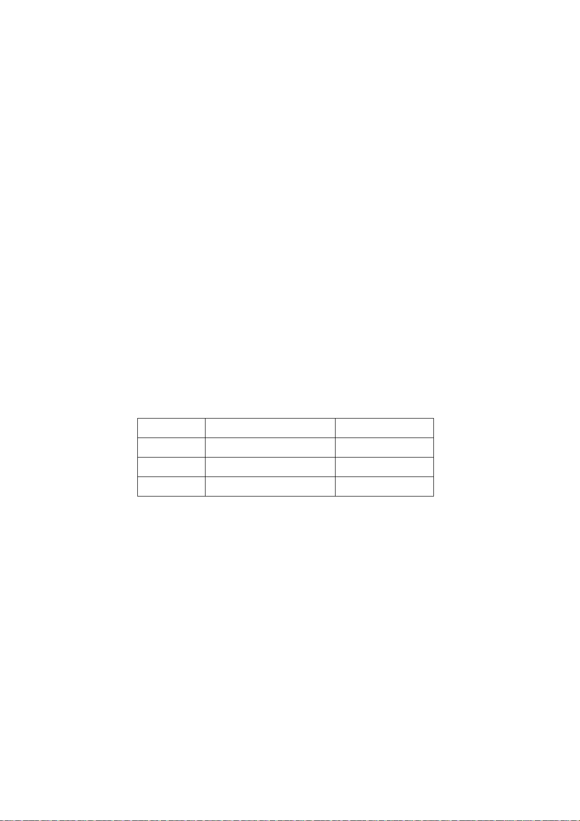
2. “Criterion for Identifying the Defects on Screen”
The PDP produced by our Company at present uses the following criterion for identifying the
defective points:
There may appear three kinds of defective points for this model as shown in Fig.1 --bright spot
(remain bright); dark spot (non-illuminating); flickering spot (remain flickering). However they
should not exceed the specification as in table 1. Otherwise the product shall be deemed as
sub-standard.
Figure 1 Defective Points
Table 1 Criterion for Three Kinds of Defective Points
Zone B
Item Kind Area A Area B Remark
1 Dark spots No more than 4 No more than 10
2 Bright spot No more than 1 No more than 3
3 Flickering spots No more than 1 No more than 3
Zone A
W
H/4
H/2
H/4
W/4 W/2W/4
Total number of defective points
in A and B shall not exceed 14.
The distance between two
defective points shall not be
shorter than 10mm.
3
Page 6
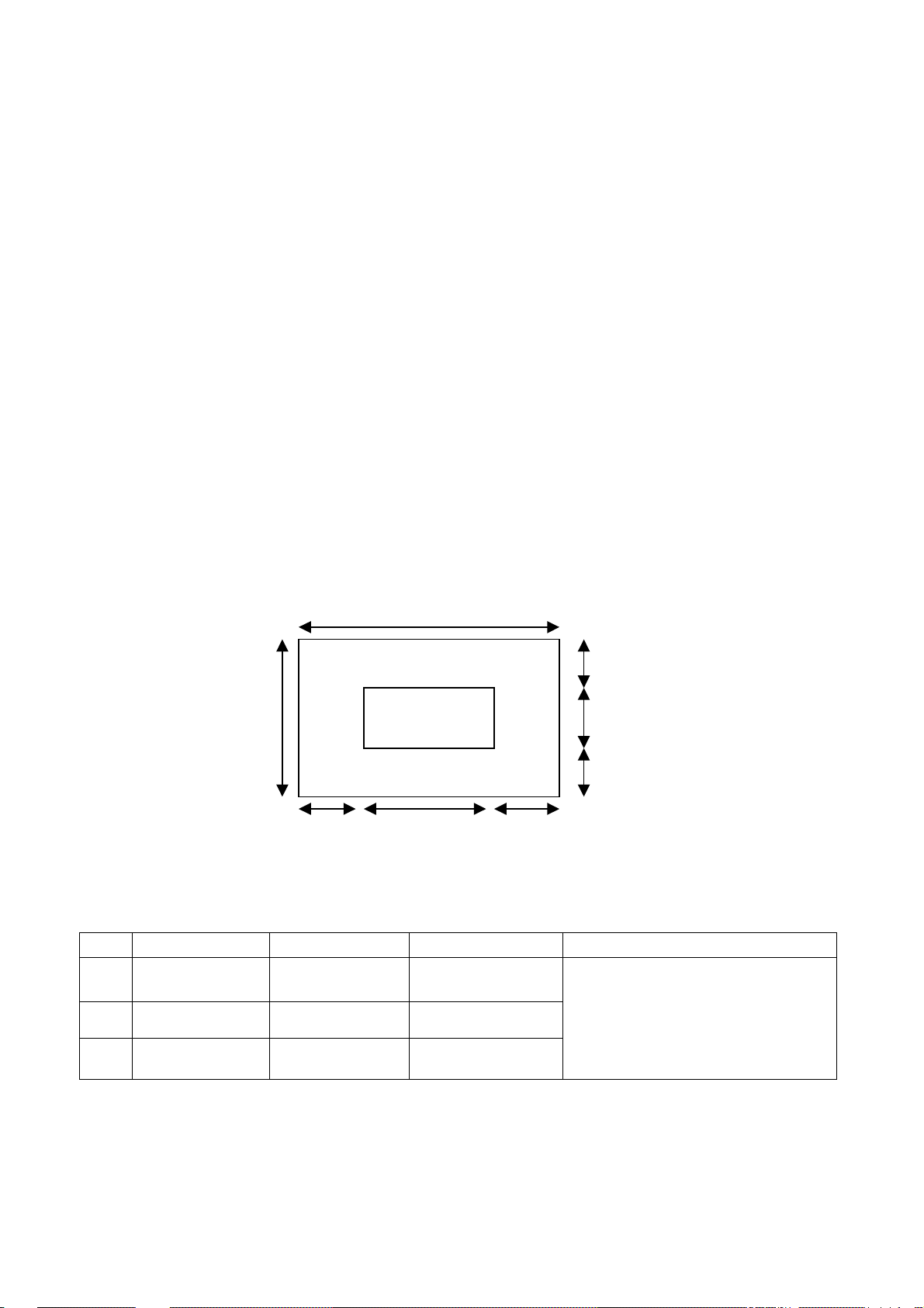
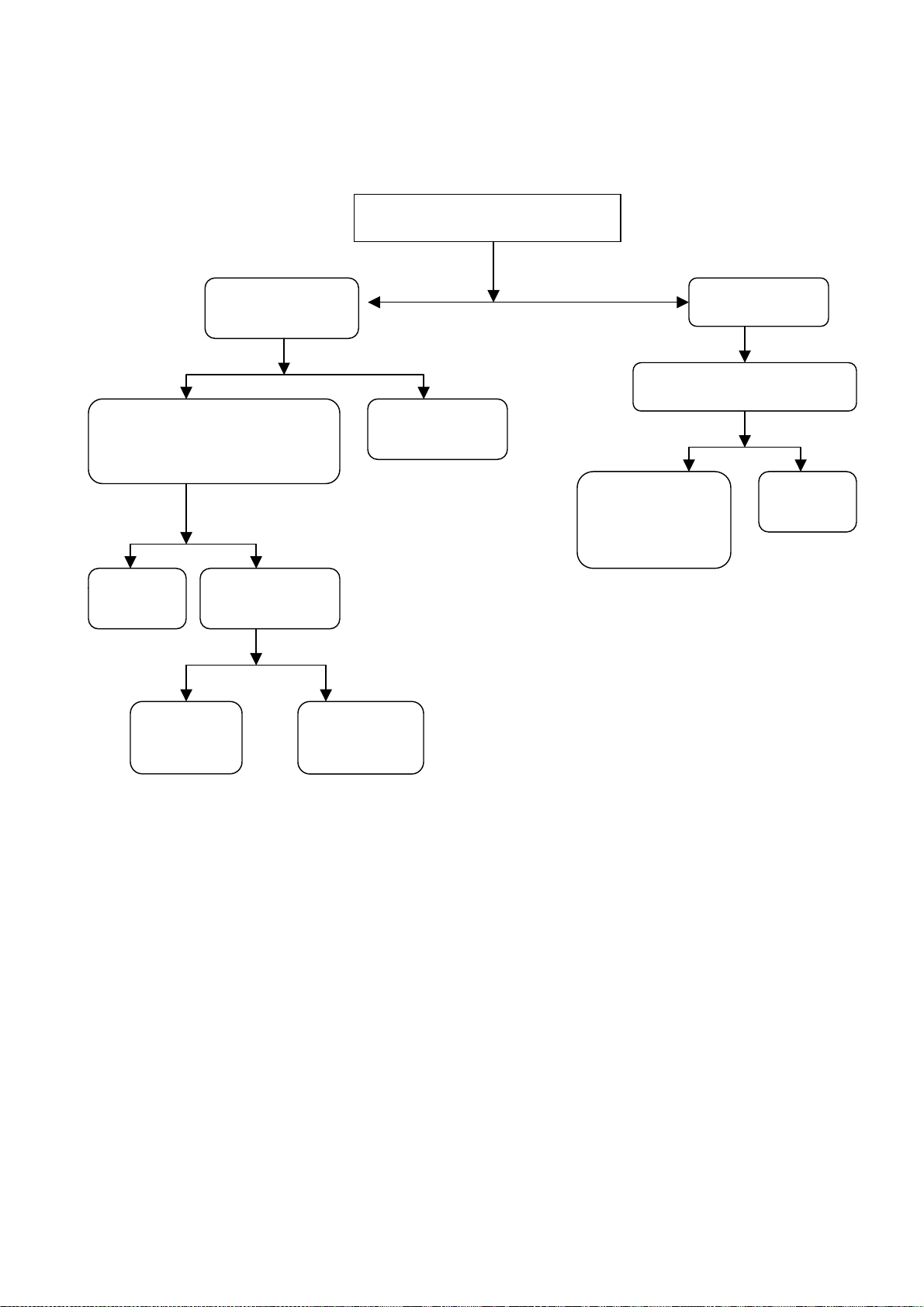
Alignment instruction
1. Alignment equipment
PM5518 (video signal generator)
K-7253 (VGA signal generator)
CA210 (white balancer)
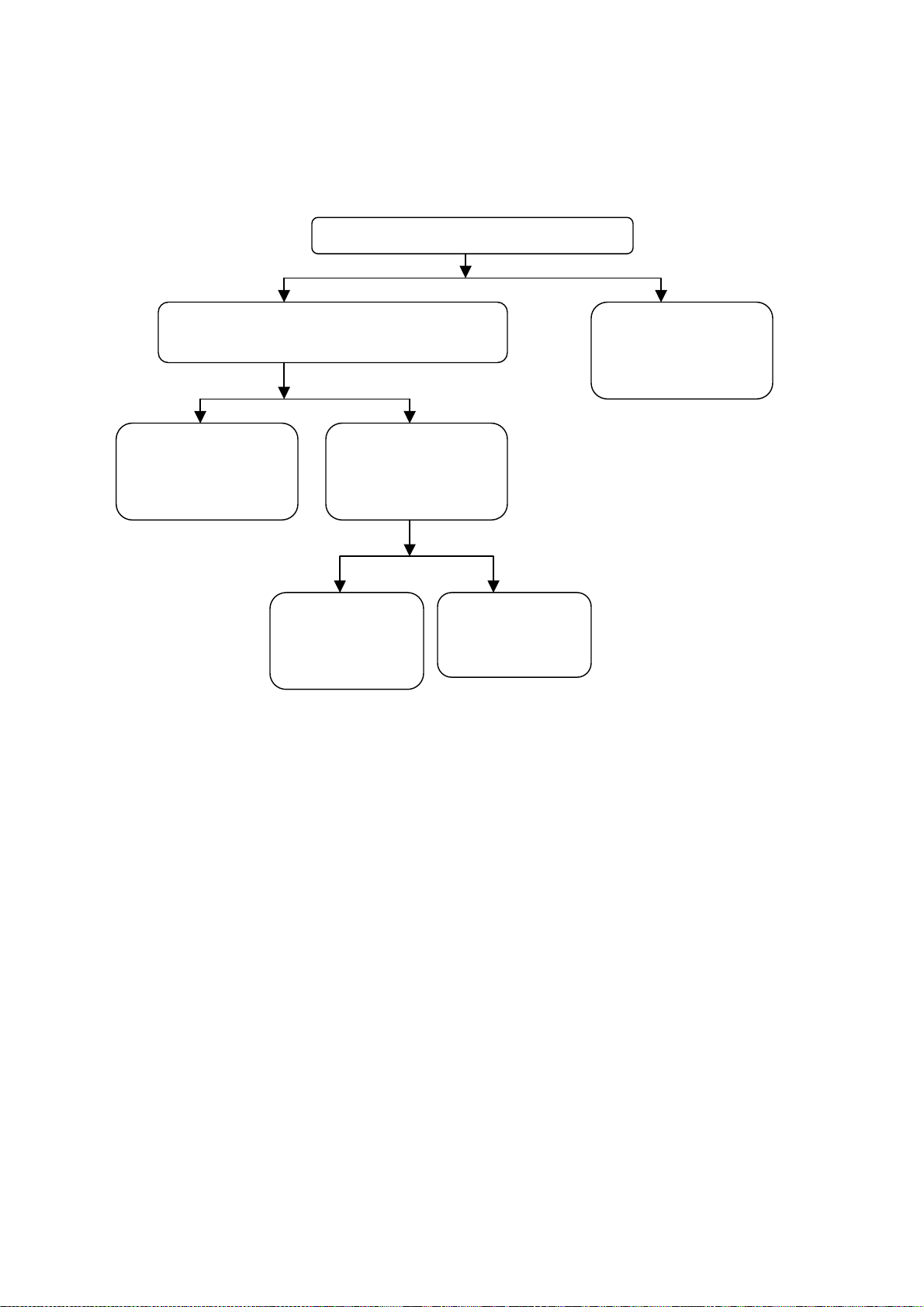
2. Alignment flow-chart
The alignment flow-chart is shown as fig-1
To produce CPU board and AV and TV board
Check AV board and TV board
Connect with central signal source, then check each function of TV such as
analog control etc., check the output of headphone and speaker
Input AV/S and HD signal, then check each function of all the terminals
Input VGA signal (one format), check if the displ ay is normal under PC
condition, check each function such as analog control etc., ch eck hori zont al
/vertical center etc.
Check the accessories and pack t hem in box
Fig-1 adjustment flow-chart
3. AV/TV board adjustments
Adjust the potentiometer VR9002 of power supply board, testing TP1(12VAMP) point is 15V ±0.05V.
4. CPU board adjustments
Connect CPU board, button board and AV/TV board, connect with power and observe the display.
Method for entering factory menu: press “VOL+”, “MUTE” and “VIDEO” repeatedly to enter factory
menu; press “ENTER” to select different items when the first line of each adjustment item just lights
up; input VGA and DVI signal, then select the “mode” item; after that, you can press “enter” to select
three kinds of color temperature namely 6500K, 9300K and 12000K press “MENU” to exit.
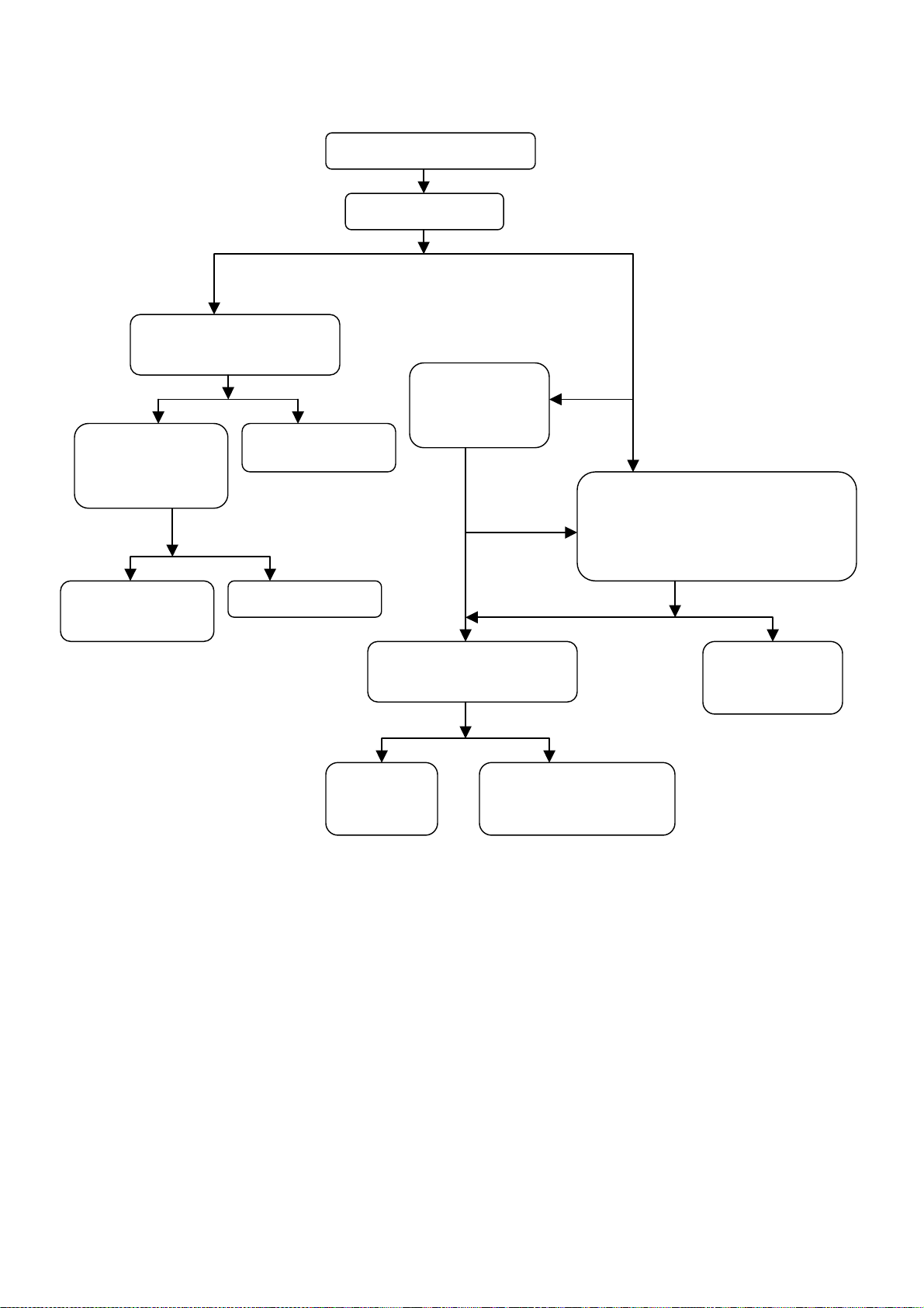
Check DDC and FLASH
Check the CPU board
All testing
4
Page 7

4.1 EEPROM initialization
Enter the first page of factory menu, select “clear eeprom” and then press “enter”, shut down the
unit after “ok” appears.
4.2 VGA channel adjustment
4.2.1 Preset VGA channel mode
Input VGA signal (PATTERN 5: Final Test) of K-7253, select TIME301 (640*350/70Hz), press
“AUTO” to do the auto adjustment until the screen is filled with picture. Use the same method to do
auto adjustment for the following items:
TIME302 (720*400/70Hz) TIME303 (640*480/60Hz) TIME311 (800*600/60Hz)
TIME313 (1024*768/60Hz) TIME315 (640*480/75Hz) TIME316 (800*600/75Hz)
TIME317 (1024*768/75Hz) TIME319 (1280*1024/75Hz) TIME339 (1280*1024/60Hz)
4.2.2 ADC adjustment of VGA channel
Input K-7253 64 level gray-scale signal of TIME303 and PATTERN474, adjust adc-gain to maxinum
and let the brightest two levels be recognized.
4.2.3 White balance adjustment VGA/DVI channel
Input K-7253 8 level gray-scale signal of TIME303(640 x 480/60Hz) and PATTERN471, enter white
balance adjustment menu; adjust the third and seventh levels using white balance.
Select 6500k of “mode”, adjustment offset_R, offset_G and offset_B, let the color coordinate of the
second level be 308 and 316 and its brightness be4.5-5nit more or less. Adjust gain_R, gain_G and
gain_B, let the color coordinate of seventh level be 308 and 316. Adjustment offset_R, offset_G,
offset_B, gain_R, gain_G and gain_B repeatedly until the value of the two levels gray-scale be 308
and 316.
Select 9300k of “mode”, adjustment offset_R, offset_G and offset_B, let the color coordinate of the
third level be 285 and 293 and its brightness be 4.5-5nit more or less. Adjust gain_R, gain_G and
gain_B, let the color coordinate of seventh level be 285 and 293. Adjustment offset_R, offset_G,
offset_B, gain_R, gain_G and gain_B repeatedly until the value of the two levels gray-scale be 285
and 290.
Select 12000k of “mode”, adjustment offset_R, offset_G and offset_B, let the color coordinate of the
second level be 270 and 283 and its brightness be 4.5-5nit more or less. Adjust gain_R, gain_G and
gain_B, let the color coordinate of seventh level be 270 and 283. Adjustment offset_R, offset_G,
offset_B, gain_R, gain_G and gain_B repeatedly until the value of the two levels gray-scale be 270
and 283.
Note: gain_R, gain_G, gain_B should not value above 128 and let one of them be 128 at
least.
4.3 Adjustment AV/TV channel
4.3.1 Adjustment VCO, OPTION, sub-brightness and sub-contrast
Input AV color bar signal (PM5518 COLOR BAR 100%) to VIDEO terminal, enter the first page of
factory menu, press “enter” after selecting “auto color”, display “OK” after 2 seconds; then you can
finish the VCO adjustment; set the value of “option” to 11 and “s-bright” to 150 as well as S-contrast
to 140. Set the Max Volume to 17 when the AVC is OFF and SRS is OFF. Set the page number of
VPC3220 to 0, 0, 3, 3, 3, 3, 9.
4.3.2 white balance adjustment of AVTV channel
Input AV signal (PM5518, 8 level gray-scale signal), enter adjustment menu of white balance, and
5
Page 8
adjust the second level and seventh level using white balance. Adjust offset_R, offset_G and
offset_B to let color coordinate of the second level be 285 and 290 and its brightness be about
2.3nit. Fixate gain_B to 128, adjust gain_R, gain_G to let color coordinate of the seventh level be
285 and 290. Adjust offset_R, offset_G, offset_B, gain_R and gain_G, repeatedly using the same
method until the value of the two levels gray-scale be the specified value.
4.4 white balance adjustment YPbPr channel
Input YPbPr signal of K-7253 to YPbPr terminal, input TIME380 (480i) PATTERN471 8 level
gray-scale signal, Enter adjustment menu of white balance, adjust the second level using white
balancer. Adjust offset_R, offset_G and offset_B, to let color coordinate of the second level be 285
and 290 and its brightness be about 2.3nit.
Input 8 level gray-scale signal of TIME392 (480p), TIME394 (720p) and TIME396 (1080i) separately,
repeat the above operations to let color coordinate of the second level be 285 and 290 and its
brightness be about 2.3nit.
5 Performance check
5.1 TV function
Enter searching menu → auto search, connect RF-TV terminal with central signal source and check
if there are channels be skipped
5.2 AV/S, YPbPr terminals
Input AV/S, HD signal, check if it is normal.
5.3 VGA terminal
Insert VGA terminal, input VGA format signal of 640 X 480@60 Hz, check if the display is normal. If
interference exists, press the auto adjusts button on remote control again and check if it is normal.
5.4 check sound channel
Check the speaker and headphone of each channel.
5.5 presetting before ex-factory
Item Setting Item Setting Item Setting
Picture mode NATURE OSD language English BALANCE 50
Sound mode NEWS VGA color
N/R WEAK SPEAKER ON CCD OFF
SCREEN 16:9 HEAD PHONE ON Turn off TV
9300 SRS OFF
temperature
6
Page 9
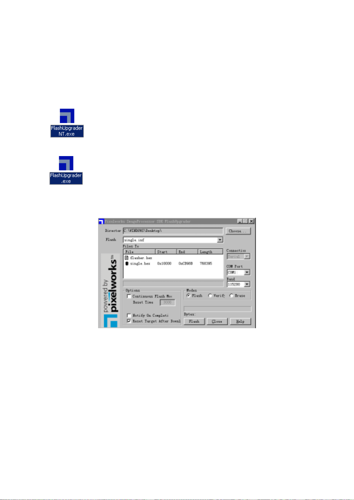
Method of software upgrading
Steps of software upgrading are as follows:
1. Select a serial connection wire and a VGA connection wire and then connect them by means of a
patch panel;
2. Use a serial wire to connect the PC to the patch panel and set TV set to off state;
Open the software upgrade file holder and double click
FlashUpgraderNT (use under window 2000/XP/NT)
FlashUpgrader (use under window 98),
The following interfaces will show up after running the program:
Based on the computer features, set up the serial port (COM Port). Select corresponding serial port
(if it’s unable to FLASH WRITE, change to another port). Baud is selected to be 115200. Then
select Reset Target After Download. Click FLASH pushbutton, it’s ready to run. For other settings,
please refer to the Fig. Above (already defaulted by the system, normally no need to change).
Switch on TV set the FLASH write program begins to run;
7
Page 10

After FLASH write is over, push button “cancel” will become flash. Then shut the main power supply
and its OK just switch it on again.
Note: Do not shut the power off or turn the TV set on during the FLASH write. Otherwise it
may lead to no way for flash to rewrite.
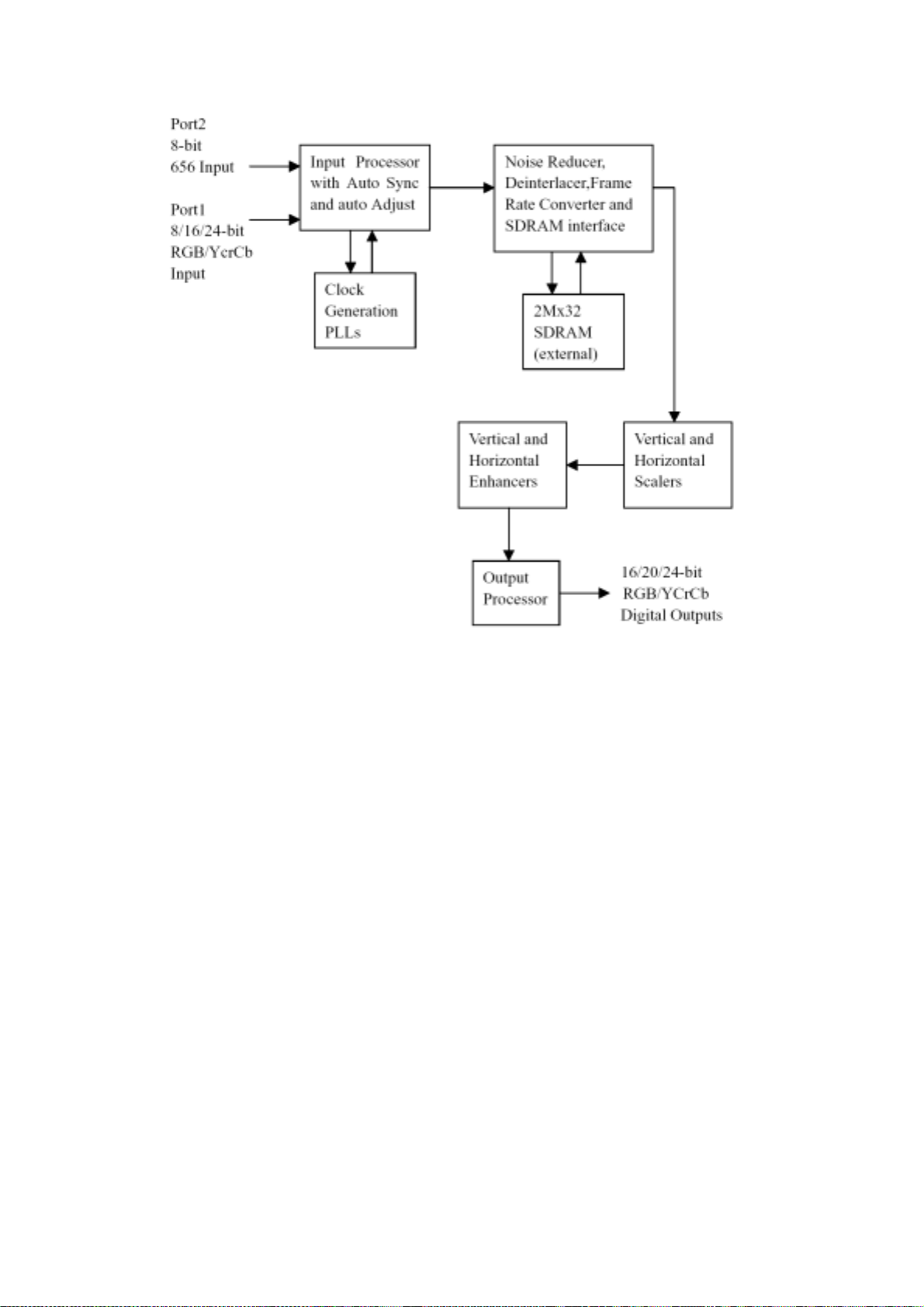
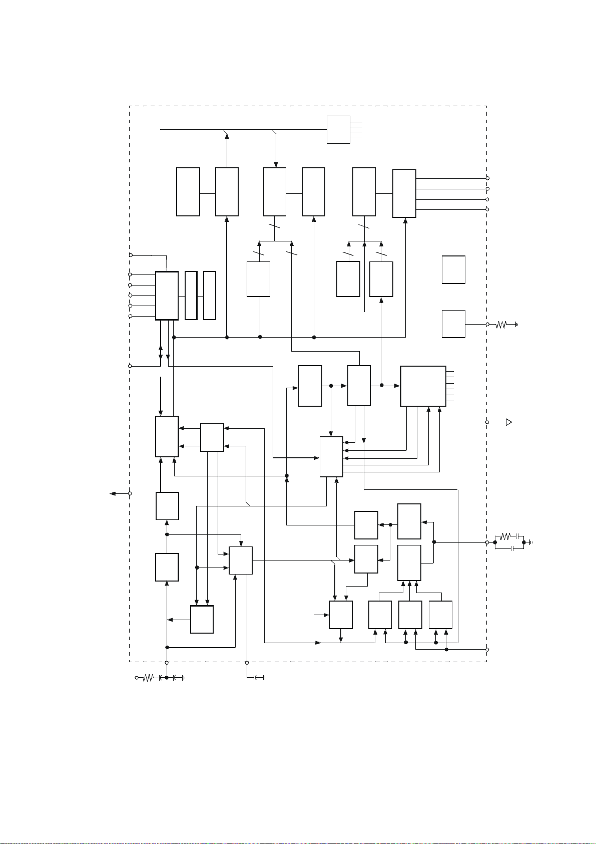
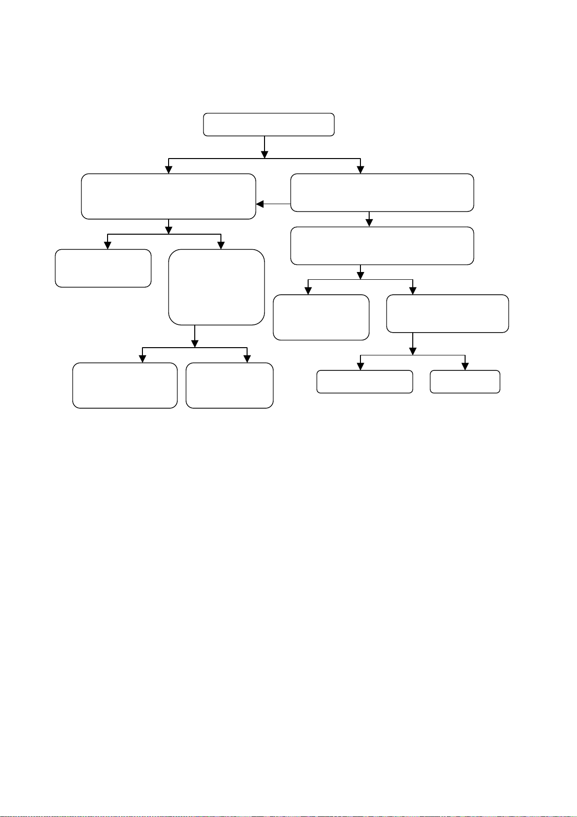
Working principle analysis
RF signal produces composite color television signal (TV-V) and second intermediate frequency SIF
through TUNA01. The signal together with AV/SVHS (SVHS priority) and VIDEO etc. are sent to
U29 VPC3230. After the above three video signals being selected, one is output as AV OUT; one is
sent to CCD decoder Z86229 (NA09) to get RGB and FB signals, then send them back to U29; the
last one is sent to do color decoding and then is sent to FLI2310 (U13) with the format of 8 bit
ITU-R656 to do line-by-line process.
YPRPB signal is firstly sent to U30 MST9883 to do the A/D conversion. After this, the signal will be
converted into YUV signal of 24BIT, send it to FLI2310 also.
After a series of procedure such as matrix, chrominance and tint etc. in FL12310, the above two
ways signal will be converted into RGB of 24bit, then send it to the main processing chip U12
JAG-ASM. There are another two signals sent to U12 also: RGB signal of computer VGA, RGB
signal of 24BIT produced by DV1 through U15 TFP403/501. The three ways of signal will be
selected and do the picture format process in U12, including items of OSD, GAMMA correction,
brightness and contrast etc., and then they will be converted into 1024*768 format in the form of
24BIT RGB signal. Send it to LVDS converter U31 DS90C383, then it will be converted into 4
low-voltage difference signals which can be accepted by PDP panel, then send it to PDP panel to do
the picture display.
Send left and right channel audio R/L of VGA/DVI to MSP3420 (NA04) after selection by HEF4052
(NA03); send AV, SVHS and R/L of YPBPR to NA04; send SIF of tuner to NA04 also. SIF of the
second sound IF will be demodulated as audio signal in NA04, the signal together with other 4 ways
of audio signals will do the conversion selection, finally volume control and sound effect processing
will be done. Output left-right sound channel signal R/L. one will be sent to SRS sound field
processor NA06 M62494 to do SRS processing and finally amplified by NA07 and NA08 TPA3001
to drive the speaker.
The power panel attached to PDP panel can supply with power, and it can be switched to all kinds of
power needed.
8
Page 11
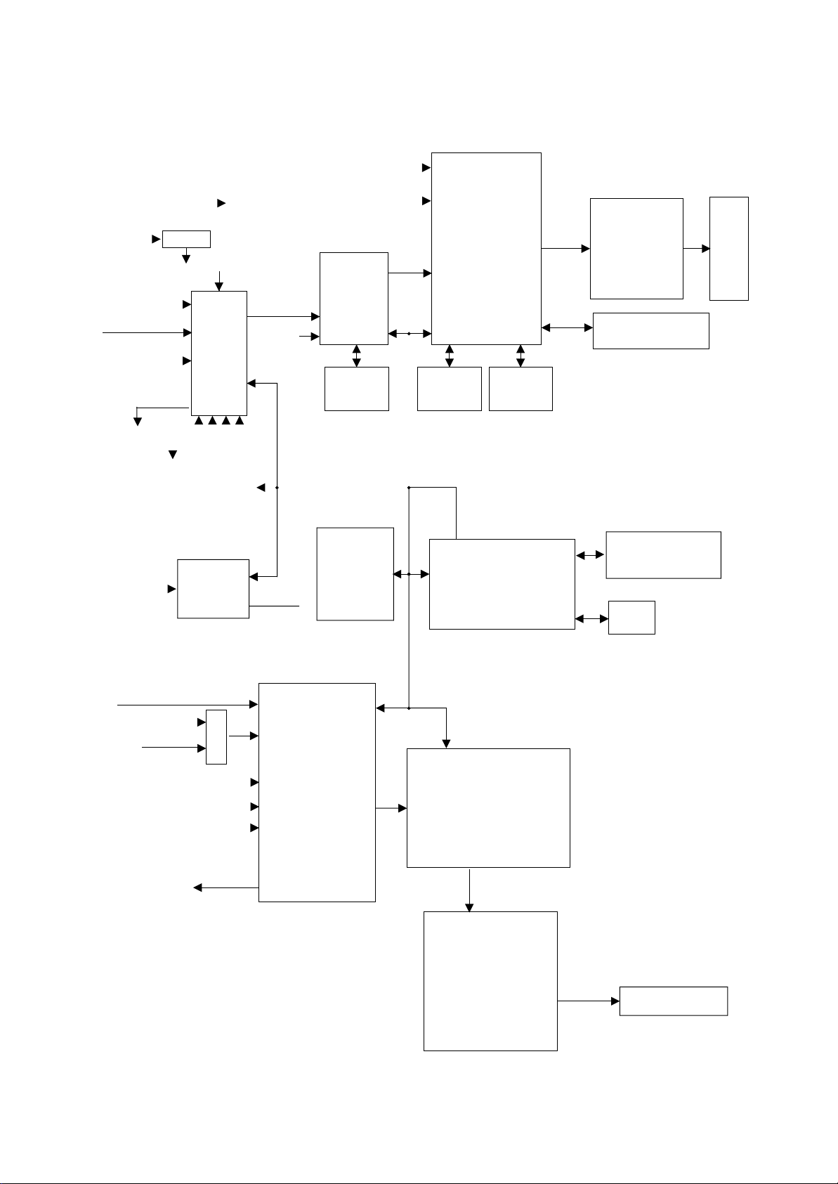
BLOCK DIAGRAM
VGA
DVI
RF
Y/AV2
C
AV1
AV-V OUT
YPrPb
TUNA01
SIF
VPC3230
V
R G B FB
NA09
CCD
Z86229
U30
ADC
MST9883
RECEIVER
TFP501
TV-v
VIDEO DECODER
ITU-R656
U29
RGB
U15
DVI
24bit
YUV
8bit
U13
DEINTER
LACER
FLI2310
U14
SDRAM
2
I C BUS
U3
EEPROM
RGB
24bit
U12
SCALER
JAG-ASM
U19
SDRAM
U20
SDRAM
U2
MICRO-CONTRLER
TSC80251G2D
RGB
24bit
U31
LVDS
DRIVER
DS90C385MTD
KEY BOARD
U4
FLASHMEMORY
IR
PANEL
SIF
VGA
DVI
YPrPb
AV1
S/AV2
AV-MONO OUT
HEF4052
NA03
MONO
NA04
AUDIO
PROCESSOR
MSP3420
R/L
NA06
SRS 3D STEREO
CONTROLLER
M62494
R/L
NA07
NA08
AUDIO
AMPLIFIER
TAP3001
9
R/L
SPEAKER
Page 12
IC block diagram
1.AD9883
Pins description:
54,48,43 PIN: Input of YPRPB
2-9 PIN: Output of Y
12-19 PIN: Output of U
70-77 PIN: Output of V
56,57 PIN: SCL, SDA applied for control the operation of IC
66 PIN: Output of horizontal synchronizing
64 PIN: Output of field synchronizing
65 PIN: Output of DE
67 PIN: Output of CLK
11,26,34 PIN: 3.3V power supply
10
Page 13
2.VPC3230
Pins description:
70 PIN: Video of AV OUT
71 PIN: Input C
72 PIN: Input Video of Y or AV2.
73 PIN: Input Video of AV1.
74 PIN: Input Video of TV
31-34, 37-40 PIN: Output format signal of. ITU-R656
27 PIN: Output of CLK
13,14 PIN: SCL, SDA applied for control the operation of IC
10,29,45,52 PIN: 3,3V_VPC power supply.
59,69,76 PIN: 5V power supply.
11
Page 14
3.FLI2310-Simplified Internal Block Diagram
Pins description:
196,199-205 PIN: Input of format signal of ITU-R656
11-15,18-20 PIN: Input of U
21-28 PIN: Input of V
29,32-35,38-40 PIN: Input of Y
1 PIN: Input of YPRPB horizontal synchronizing
2 PIN: Input of YPRPB field synchronizing
4 PIN: Input of YPRPB-CLK
5 PIN: Input of YPRPB-DE
195 PIN: Input of AV/TV-CLK
114 PIN: Input of SDRAM-CLK
136,137,140-145 PIN: Output of R
148-155 PIN: Output of G
126,127,130-135 PIN: Output of B
125 PIN: Output of CLK
111 PIN: Output of SDRAM-CLK
118 PIN: Output of horizontal synchronizing
119 PIN: Output of field synchronizing
120 PIN: Output of enable
45,46 PIN: SCL, SDA applied for control the operation of IC
8,62,112,193,171,187 PIN: 3.3V power supply
155,168,16,68,123,197 PIN: 1.8V power supply
12
Page 15

4.JAG-ASM
Pins description:
A12, A13: Input of VGA-R
A16, A17: Input of VGA-G
A20, A21: Input of VGA-B
P1, P2, N2, N3, M1-M4: Input of DVI-B
13
Page 16

L1-L4, K2-K4, J1: Input of DVI-R
J2-J4, H1-H3, G1, G2: Input of DVI-G
AA2, AA3, Y1-Y3, N1-N3: Input of AV/TV/YPRPB-B
N4, V1-V4, U1-U3: Input of AV/TV/YPRPB-G
U4, T1-T4, R1-R3: Input of AV/TV/YPRPB-R
AB3: Input of DVI horizontal synchronizing
AB1: Input of DVI field synchronizing
G4: Input of DVI-CLK
F1: Input of DVI-DE
D6: Input of VGA horizontal synchronizing
P3: Input of VGA field synchronizing
F2: Input of AV/TV/YPRPB horizontal synchronizing
G3: Input of AV/TV/YPRPB field synchronizing
P4, AA4, AF12: Input of A V/TV/YPRPB-CLK
G6: Input of AV/TV/YPRPB-DE
AD13-15, AE13-15, AF14, and AC15: Output of R
AF15, AC16, AD16, AE16, AD17, AE17, AF17, AC18: Output of G
AD18, AE18, AF18, AC19, AD19, AE19, AD20, AE20: Output of B
AE21: Output of horizontal synchronizing
AC21: Output of field synchronizing
AC13: Output of CLK
AF20: Output of EN
AD21: Output of EN VDD(power switch)
AF22: Output of EN BKL(back light switch)
B1: Output of PWW(back light adjustment)
F3, F4: SCL, SDA applied for control the operation of IC
B22,C22,D20,C21;H4;D21;AC8: 2.5V
D7;A5;A26;AF10: 3.3V
C10,D10-D19: JA2.5V1
C8,D8,D9: JA2.5V2
14
Page 17
5. TFP501
functional block diagram
3.3 V
Internal 50-
Termination
3.3 V
1.8 V
Regulator
3.3 V
Rx2+
Rx2-
Rx1+
Rx1-
Rx0+
Rx0-
RxC+
RxC-
RED(0-7)
CTL3
CTL2
GRN(0-7)
CTL1
BLUE(0-7)
VSYNC
HSYNC
Panel
Interface
Latch
Latch
Latch
PLL
Channel 2
Channel 1
Channel 0
Data Re co ver y
and
Synchronization
+
_
+
_
+
_
+
_
CH2(0-9)
CH1(0-9)
CH0(0-9)
TMDS
Decoder
QE(0-23)
QO(0-23 )
ODCK
DE
SCDT
CTL2
CTL1
VSYNC
HSYNC
Terminal Functions
TERMINAL
NAME NO.
AGND 79 GND A nalog ground? Ground reference and current return for analog circuitry
AV
DD
82,85,88,91V
CAP 67 V
CTL[2:1] 41,40 DO General-purpose control signals? Used for user defined control. In normal mode CTL1 is not powered down
DE 46 DO Out put data enable? Used to indicate time of active video display versus nonactive display or bl ank time.
DFO 1 DI Ou tput cl ock data forma t? Contro ls the o utput c lock ( ODCK) f ormat for eith er TFT o r DSTN panel su pport . For
DGND 5,39,68 GND Digital ground? Ground reference a nd current return for digital core
DV
DD
6,38 V
HSYNC 48 DO Hor i z ontal sync output
OCK_INV 100 DI ODCK polarity? Selects ODCK edge on which pixel data (QE[23:0] an d QO[23:0]) and control signals
I/O DESCRIPTION
I/O
Analog VDD? Power supply for analog circuitry. Nominally 3.3 V
DD
Bypa ss c apa ci t or? 4.7F tantalum and 0.01 F ceramic conn ected to gro und. This ca paci tor is o ptiona l for
DD
the TFP403, but is required for the TFP501.
.
via PDO
DESCRIPTION
During blank, on ly HSYNC, VSYNC, and CTL1-2 are tr ansmitted. During tim es of active display , or nonbla nk,
only pixel data, QE[23:0] and QO[23:0], is transmitted.
High : Active display time
Low: Blank time
TFT support ODCK clock runs cont inuously . For DST N support OD CK only clock s when DE is high; ot herwise
ODCK is held low when DE is low .
High : DSTN support/ODCK held low when DE = low
Low: TFT support/ODCK runs continuously.
Digital VDD? Power supply for digital core. Nominally 3.3 V
DD
(HSYNC, VSYNC, DE, CTL1-2 ) are latched
Normal mode:
High : Latches output data on rising ODCK edge
Low : Latches output data on falling ODCK edge
80,81,83,84,86,87,89,90: Input of four DVI different signal
92: DDC-SCL
93: DDC-SDA
95: PROM-SCL
96: PROM-SDA
2: Input of POWER DOWN
15
Page 18
9: Input of OUTPUT DRIVE POWER DOWN
8: Output of synchronization check
10-17: Output of B
20-27: Output of G
30-37: Output of R
44: Output of CLK
46: Output of data enabling
47: Output of field synchronizing
48: Output of horizontal synchronizing
6,38,82,91,18,29,57,78,97: 3.3V power supply
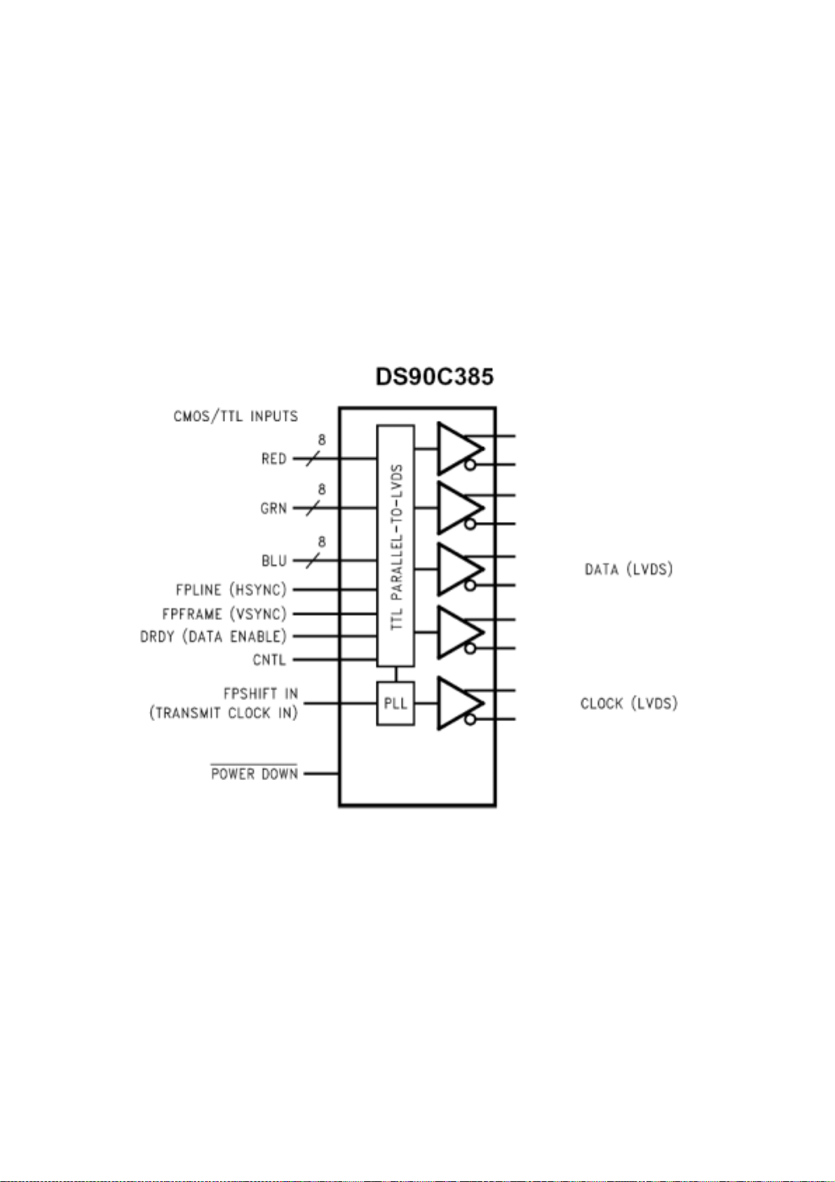
6. DS90C385
51,52,54-56,3,50,2: Input of R
4,6,7,11,12,14,8,10: Input of G
15,19,20,22-24,16,18: Input of B
27: Input of horizontal synchronizing
28: Input of field synchronizing
30: Input of data enabling
31: Input of CLK
32: Input of power enabling
37,38,41,42,45,46,47,48: Output of 4different signal
39, 40: Output of 1 CLK signal
1, 9, 26, 34, and 44: 3.3V power supply
16
Page 19
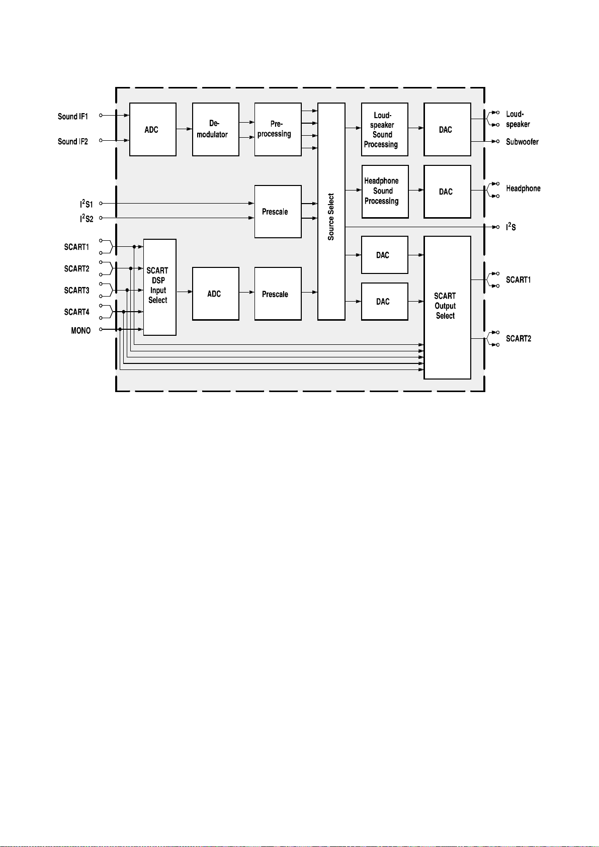
7. MSP3420
47: Input of VGA/DVI-L
48: Input of VGA/DVI-R
50: Input of YPRPB -L
51: Input of YPRPB -R
53: Input of AV2/S -L
54: Input of AV2/S -R
56: Input of AV1-L
57: Input of AV1-R
67: Input of SIF
25: Input of earphone -L
24: Input of earphone -R
27: Output of R
28: Output of L
36: Output of AV-R
37: Output of AV-L
2: SCL
3: SDA
11,12,13; 39; 65,66: +5V—MSP
17
Page 20
8. Z86229
AddrB us
Row
1
6 4 15 14 1613
VDD
+5V
I2CSEL
SDO
SDA
SCK
Serial
SEN
SMS
VIN/
Intro
Data Line
Sliced
12
Data CLK
Data
Data
Buffer
Status Reg
Control Port
Data Bus
FEW
Recovery
AW
Slicer
Lock
VW
SIG
Processor
Command
TestReg
II Lock
Digital
PG
Slicer
SYNC
MUX
Address
10
4
Row
Latch
Display
6
DOT CLK
DOT CLK
DEC
ADDR
RAM
DIV
CHAR CLK
VLock
COMP SYNC
ADDR
Decoder
RED
GREEN
POR
V/I
CKT
Ref
Line & Fld
BLUE
BOX
17 3 2 18
Z86229 only
10
RREF
Decodes
Vss(A)
11
Loop
Filter
9
LPF
Logic
Character
Generator
13
8
Latch
Display
FLD
CIR
CHAR
CW
MSGR
OSCO/S
Output
4
SS CTR
Field
Line &
Control
LS
SLS
SFLD
FLD
Control
&MUX
IDrive
CG
Dual
Clamp
Slice Level
7
Video
8
CSYNC
CG Lines
Logic
PH1
MSYNC
PH2
Figure 1. Z86229 Block Diagram
FR
HIN
5
18
Page 21
Wiring diagram
SPEAKER ASSY
POWER SUPPLY
FILTER BOARD
667-PSIK8U-40
AV PROCESSING BOARD
POWER SUPPLY BOARD
PANEL
CPU BOARD
LOGIC BOARD
667-PSIK8U-56
BUTTON BOARD
19
Page 22
Main assembly
NAME NO. MAIN COMPONENT AND NO.
AV processing board 667-PSIK8U-40 NA04
NA06
NA07
NA08
NA09
CPU board 667-PSIK8U-56 U12
U13
U15
U29
U30
U31
U2
U4
U15
Keypad board 667-PS42K8-05
Power supply filter board 667-PS42D8-51
Panel (S42SD-YB03) 335-42003-00
MSP3420 (353-34200-10)
M62494FP (353-62494-20)
TPA3001 (353-30010-10)
Z86229 (353-86229-10)
JAG-ASM (353-0JAG0-00)
FLI2310 (353-23100-00)
TFP403PZP
(353-04030-10)
VPC3230D (353-32300-80)
MST9883B (353-98830-10)
DS90C385 (353-03830-70)
TSC80251G2D (353-80251-10)
AT49F002NT (352-49002-70)
TFP501 (353-05010-00)
20
Page 23
Trouble shooting
Before servicing please check to find the possible causes of the troubles according to the
table below.
1.Antenna (signal):
Picture is out of focus or jumping Bad status in signal receiving
Poor signal
Check if there are failures with the electrical connector
or the antenna.
Check if the antenna is properly connected.
Fringe in picture Check if the antenna is correctly oriented.
Maybe there is electric wave reflected from hilltop or
building.
Picture is interfered by stripe
shaped bright spots
There appear streaks or light color
on the screen
2.TV set:
Symptoms Possible cause
Unable to switch the power on Check to see if the power plug has been inserted
No picture and sound Check to see if the power supply of TV has been
Deterioration of color phase or color
tone
Screen position or size is not proper Check is the screen position and size is correctly set
Picture is twisted and deformed Check to see if the picture-frame ratio is properly set
Picture color changed or colorless Check the “Component” or “ RG B” set t ings of the TV
Possibly due to interference from automobile, train, hig h
voltage transmission line, neon lamp etc.
Maybe there is interference between antenna and power
supply line. Please try to separate them in a longer
distance.
Maybe the shielded-layer of signal wire is not connected
properly to the connector.
Check if interfered by other equipment and if interfered
possibly by the equipment like transmitting antenna,
non-professional radio station and cellular phone.
properly into the socket.
switched on. (As can be indicated by the red LED at
the front of the TV set)
See if it’s receiving the signal that is transmitted from
other source than the station
Check if it’s connected to the wrong terminal or if the
input mode is correct.
Check if the signal cable connection between video
source and TV set is correct.
Check if all the picture setups have been corrected.
up.
up.
21
Page 24

set and make proper adjustment accor ding to the
signal types.
Picture too bright and there is
distortion in the brightest ar ea
Check if the contrast setting is too high.
Possibly the output quality of DVD broadcaster is set
too high.
It maybe also due to improper terminal connection of
the video signal in a certain position of the system.
Picture is whitish or too bright in the
darkest area of the pictur e
Check if the setting for the brightness is too high
Possibly the brightness grade of DVD player
(broadcaster) is set too high.
No picture or signal produced from the
displayer if “XXX in search” appears.
Check if the cable is disconnected.
Check if it’s connected to the proper terminal or if the
input mode is correct.
There appears an indication - “outside
the receivable scope)
Check if the TV set can receive input signal. The
signal is not correctly identified and VGA format is
beyond the specified scope.
Remote control cannot work properly Check if the batteries are installed in the reverse
order.
Check if the battery is effective.
Check the distance or angle from the monitor.
Check if there is any obstruct between the remote
control and the TV set.
Check if the remote control signal- receiving window
is exposed to strong fluorescence.
No picture and sound, but only hash. Check if the antenna cable is correctly connected, or
if it has received the video signal correctly.
Blur picture Check if the antenna cable is correctly connected.
Of if it has received the right video signal.
No sound Check if the “mute” audio frequency setting is
selected.
Check if the sound volume is set to minimum.
Make sure the earphone is not connected.
Check if the cable connection is loose.
When playing VHS pictur e sear ch
tape, there are lines at the top or
bottom of the picture.
When being played or in pause VHS picture search
tape sometimes can’t provide stable picture, which
may lead to incorrect display of the liquid cr ystal TV,
In this case please press “auto” key on the remote
control so as to enable the liquid crystal TV set to
recheck the signal and then to display correct picture
signal
22
Page 25
Troubleshooting charts
t
d
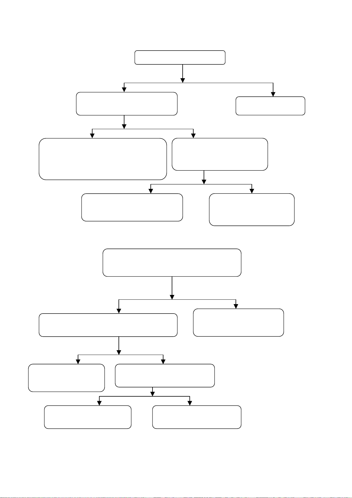
1.No raster, no picture and no sound:
Check if power indication is light?
yes no
normal
Short circuit the pin 8 (PS-ON) of
P2 to the ground, then check the
supply power.
JI
U24
abnormal
Normal abnormal
Note: Power supply for PDP i s pr ovided with over current and over voltage protection functions.
If there is over current or over voltage, this protection will function and no output.
Short circuit in
a power line
Check the supply
power D3.3V
abnormal
abnormal normal
Pull out P2 check
power
Power board
problem
No raster, no picture and no sound
Check U2 an
U4
Check 5V-STBY
Pull out P2 check 5V-STB
Short circuit U24
and other circui
of side.
abnormal normal
Power board
problem
23
Page 26
2.With sound but no picture:
b
yes no
no yes
Check if the white
alance of the factory
menu is normal?
normal
abnormal
Check all signal for
Normal abnormal
this circuit
Normal abnormal
Note:
Setting for the self check of the screen:
For 42”HD screen (S42AX-XB01):Push down 2 and 4, push up 3 of SW2001on the logic board;
For 50”HD screen (S50HW-XD02):Push down 1 and 4, push up 2, 3, 5, 6 of SW2001on the logic
board;
Please make sure resume it to the original status when the check is over.
Check if no image for all
other channels
check program
yes no
Reset the EEPROM
With sound but no picture
Display LOGO?
Check if the P4
is signal wave?
Check input signal of U31
and power supply
U31
damaged
Check U12 and the
circuit of output part
Unfix P4 and P2, short circuit the PIN8
of the P2 to END, testing signal itseft of
the logic board set the on, then check if
display white of the panel.
Screen damaged
24
Page 27
3.With picture but no sound.
d
r
k
v
p
t
p
y
y
With picture but no soun
If there is output from XA01of sound power amplification board
No
Yes
Check if input signal in pin 2 of sound
power amplification
Sound box damaged
yes no
Sound power amp. or other peripheral circuit have
problem. Check power supply, if SHUTDOWN pin
control is normal and if output short circuited or othe
problems that cause protection to work.
Measure if the sound input of the
present channel corresponding to
no
yes
MSP3440 or other peripheral
circuit have problem
Check different levels of circuit
following input audio signal
4.A certain channel is abnormal
1) AV/YCRCB no picture
Check if pin 72(S-VIDEO), pin73(VIDEO),
pin75/pin5(YCRCB) of U29 has signal input
yes no
Check if pin27, pin31-34, pin37-40 of U29 has loc
signal output and ITU-R 656 is normal?
There is problem from A
socket to U29 channel
no
es
U29 or other peripheral
circuit have problem
Check PR3~PR9 resister to see if
U13 out
ut is normal
no
es
U13 or other peripheral circui
have problem
U12 or other peripheral circuit have
roblem
25
Page 28
r
y
y
y
2) No picture in YPrPb
Check if pin48 and pin49 of U30 have input signal.
es
no
Check U30 and other
peripheral circuit
Check PR36-RP41 and RP141 resiste
to see the U30 output is normal?
no
Check D4 socket to U30
signal.
es
Check PR3-RP9 resister to see the U13
output is normal?
Check U13 and other
peripheral circuit
no
es
Check U12 and other
peripheral circuit
26
Page 29
k
r
r
y
y
y
3) TV no picture
.
Check if pin27, pin31-34, pin37-40 of U29 has loc
signal output and ITU-R 656 is normal?
Check U29 and othe
peripheral circuit
Check if PIN74 of U29 have input signal?
es no
es no
Check PR3~PR9 resiste
to see if U13 output is
normal?
Check U13 and
other peripheral
circuit
esno
Check U12 and
other peripheral
Check power supply
of TUNA01 and other
peripheral circuit
27
Page 30
)
y
y
y
yesy
y
y
4) VGA No Picture
Check U12 and other
Check the input H/V synch. signal of
pin8 and pin10 of U17
es no
Check the input
peripheral circuit
es
check U17 and other
peripheral circuit
H/V synch. signal
of pin3 and pin5
of U17
check interface
circuit
Display input signal?
es
no
no
no
If the mode of VGA (lower right corner
of screen OSD
Check the input signal of PIN(A13, A17,
A21) of U12
es no
check interface
circuit
Reset EEPROM
identifiable
Check white balance of
factor
no
menu
es
Check U12
5.Abnormal picture:
Peculiar color, which may be caused by the following phenomena:
A certain differential wire pair of LVDS(RX0+/-, RX1+/-, RX2+/-, RX3+/-)of P4 is abnormal, which
may lead to lack of color ( it’s not a complete loss of color);
Failure with resistor rows RP28~RP33, w hi c h may lead to loss of correspond ing color from the gray
degree corresponding to the picture of all channels and OSD.
Failure with resistor rows RP36~RP41, w hi c h may lead to loss of correspond ing color from the gray
degree corresponding to the picture of channels D4.
Failure with resistor rows RP3~RP8, which may lead to loss of corresponding color from the gray
degree corresponding to the picture of channel D4, TV, AV and Y CRCB.
Abnormal picture vertically or horiz ont ally (bar l ike): Abnormal in complete line extend ing a ll t he way
from up downward on the screen of stand definition TV set; abnormal vertically on half screen of high
definition TV set. They may be caused by the damage of the address BUFFER module that directly
corresponds to its position, or may be caused by the damage of the connection wire that directly
corresponds to the position of the screen. The horizontal bar like abnormality is also related to the Y
driving circuit that corr esponds directly to its p osition . To judge these phenomena, It’s poss ible to chec k it
by setting the screen to the status of self check as explained above
No brightness in the square block area: Normally it’s caused by the damage of the address
28
Page 31

BUFFER module that directly corresponds to its position, or may be caused by the damage of the
(
(F)
(G)
connection wire that directly corresponds to the position of the screen. To judge these phenomena, It’s
possible to check it by setting the screen to the stat e of self check as explained above.
Diagnosis for panel and service of TV
As shown in the figure below, PDP screen can be divided into power supply board, X driving board, Y
driving board, logic board, logic BUFFER board (E, F, G), Y BUFFER board (up and down), COF etc.:
Y BUFFER(up)
Y driver board
Y BUFFER(down)
Logic
BUFFER
E)
Logic
BUFFER
Power supply board
Logic board
X driver board
Logic
BUFFER
* Power supply board: to supply power for the screen, other funct ion al modu l es on the screen, our ow n
main board, and video processing board.
* X driving board: t o produce and provide driving signal for X electrode accor ding to the time sequence
signal sent from logic board.
* Y driving boar d: to produce and provide driving signal for Y electrode according to the time sequence
signal sent from logic board.
*Logic board: to process the image signa l sent fro m the main bo ard, to pro d uce addres sin g s ignal and
to provide driving signal for X and Y driving boards.
*Logic BUFFER board (E, F): To convert the data signal and control signal sent from the logic board
into the signals required by COF
*Y BUFFER board (Upper, Lower): To transmit the scanning signal from the Y driving board to the
screen, which is divided into upper and lower parts.
*COF: to convert the signal sent from the logic BUFFER board into the address signal used by the
screen.
Troubl e diagnosis:
1.The screen is not bright:
a. Check to see if the power supply plug from the power filter board to the power supply board is well
inserted into the socket. If not, plug it in.
COF (7 blocks)
29
Page 32

b. Check if the fuse on the power supply board is blown up. If yes, replace it for a good one.
SW200
c. Remove our main board and the video processing board, ground the pin 4 POWER_ON/OFF of
socket CN802 of the power supply board,
Weld point
and then push the slide switch SW2001 on the logic board to the interna l mo des (1, 3 up and 2, 4 down)
from external modes (1, 2, 4 up and 3down)
1
Switch the power on and see if the screen is lit. If the screen can give a normal and completely white
field signal, then the problem lies in our main board or video processing board, which will be dealt with
separately.
d. If the screen is not lit, then first replace the power supply board to see if the problem is solved.
e. If the problem remains after the power supply board is replaced, then the problem lies in the screen.
Replace the entire screen for treatment.
2.There appears on the screen a line or several unlit lines.
30
Page 33

Check if the socket between Y driving board and Y BUFFER is plugged well. If not, plug it well. If yes
then replace Y BUFFER (upper, lower) in respect to the upper, lower part of the dark line on the screen.
3.There appear on the screen one or several horizontal lines that are much brighter than the remaining
horizontal lines at the edge:
Check if the socket between Y driving board and Y BUFFER is plugged well. If not, plug it well. If yes
then replace Y BUFFER (upper, lower) in respect to the upper, lower part of the dark line on the screen.
4.There appear on the screen one vertical unlit line or a vertical entirely unlit block
a. If it’s one vertical unlit line, then COF has problem.
b. If it’s a vertical entirely unlit block, then first check if the connection socket between COF and logic
BUFFER has problem. If not, check if the connection sockets between the logic BUFFER and the logic
board is normal. If yes, replace the logic BUFFER. Finally, if the problem still remains when the
replacement is over, then replace the logic board.
5.There appears on the screen a mono color signal and one or several vertical bright lines of other
colors:
a. If it’s a vertical bright line of other colors, then the problem lies with COF or the screen.
b. If it’s an entire vertical block of other colors, t hen first check to see if the connection so c ket betwee n
31
Page 34

COF and logic BUFFER has problem. If no problem, check if the connection sockets between the logic
BUFFER and the logic board is normal. If it’s normal, then replace the logic BUFF ER. I f the probl em still
remains after the replacement, then replace the logic board. Finally if the problem is still there, then the
problem lies with COF.
6.There appear on the screen abnormal bright spots or blocks that are different from what’s described
above:
a. Check if the connection socket between COF and logic BUFFER board has been well plugged.
b. Replace the logic BUFFER board. If it’s not solved then replace logic board. If the problem still
remains, then it’s the problem with COF.
32
Page 35

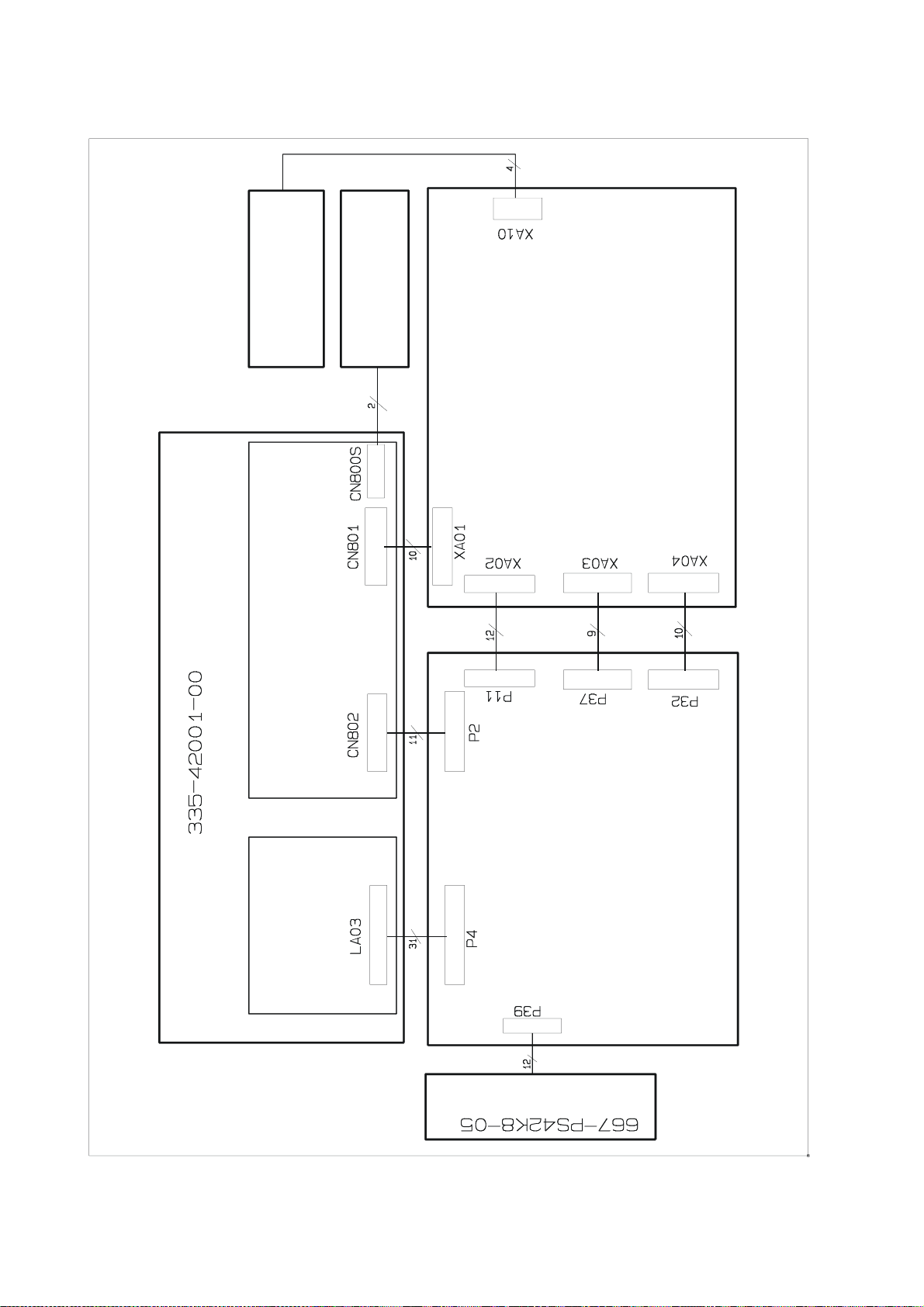
Printed circuit boards
33
Page 36

34
33
Page 37

35
Page 38

36
Page 39

Page 40

Page 41

Page 42

Page 43

Page 44

Page 45

Page 46

Page 47

Page 48

Page 49

Page 50

Page 51

Page 52

Page 53

Page 54

Page 55

EXPLODED VIEW
21
19
18
17
16
15
14
13
12
11
10
24
9
8
7
6
25
29
30
31
32
33
5
4
3
2
1
Page 56

PS-42K9
PART LIST OF EXPLODED VIEW
NO. DESCRIPTION PART#
1 SOUND BOX COVER 808-10722-AF0
2 LEFT COVER 808-10717-AF0
3 SOCKET 364-44206-00
4 REAR PANEL 804-2K445-AF0
5 REAR CABINET 780-I08RH-AFCA
6 CPU BOARD ASSY 667-PSIK8U-56A
7 MAIN BOARD FRAME 863-6B168U000
8 DISPLAY SCREEN 335-42009-00
9 PRESS BOARD 803-30204-00
10 FILTER GLASS 740-10111-00
11 SOUND BOX FIXED BOARD 804-20337-AF0
12 SOUND BOX REAR CABINET 780-30134-AF0
13 SPEAKER 384-41508-50
14 SOUND BOX FRONT CABINET 780-30133-120
15 SOUND BOX FRONT COVER 808-10721-AR0
16 BUTTON 877-60593-0T0
17 FRONT CABINT 780-I09L2JAR2A
18 BUTTON BOARD ASSY 667-PS42K8-05
19 LED COLUMN 700-60226-00A
21 POWER BUTTON 877-60593-0T0
22 SOUND BOX STAND COLUMN
24 CONVERSION BRACKET 870-10168-00
25 AV PROCESSING BOARD ASSY 667-PSIK8U-40A
26
27
28
29 POWER SOCKET 364-23212-00
30 RIGHT COVER 808-10718-AF0
31 MIDDLE COVER 808-1A719-AF0
32 HOLDER ASSY 615-10457-05
33 LINE CLASP 742-30078-020
Page 57

PART LIST
PART# DESCRIPTION LOCA.NO.
100-PS42K90-18 PS-42K9D
100-PS42K90-04 PS-42K9 02
335-42009-00 DISPLAY SCREEN S42SD-YD07 !
364-23212-00 POWER SOCKET DNF201-G-10A
364-41207-00 ANTENNA SOCKET HR-F
364-44206-00 SOCKET WP4-7
485-10144-00 POWER CORD LAP-31+LAS-13 !
488-10012-00 BATTERY 7#( made in china
602-PS42K9-03 SCHEMATIC DIAGRAM
604-PS42K97-00 OWNER'S MANUAL(DIGISTAR)
615-10459-00 TRANSOM ASS'Y
644-10184-05 IMITATEUL1015 18# 100mm YELLOW /GREEN
655-41201-283 (4-PINS) LEAD WITH HOUSING
665-D0002-421 VIDEO LINE BLUE GREEN RED
665-D0002-422 VIDEO LINE YELLOW WHITE RED
665-D0002-438 SOUND LINE 2M
665-D0002-615 LVDS LINE 31-PINS 210mm
700-60226-00A LED COLUMN
740-10111-00 FILTER GLASS 42"P2
741-10001-02 WIRE FIXED BLADE
742-30032-00 TIE
742-30038-00 TIE
742-30038-00 TIE
770-15151-71 IMITATEUL1672 22# 150mm BROWN
770-15151-76 IMITATEUL1672 22# 150mm BLUE
780-I08RH-AFCA BACK CABINET ( GREY 05,SILK-SCREEN )
780-I09L2JAR2A FRONT CABINET (ABS V0 BLACK ,SILK-SCREEN )
803-30204-00 LEFT PRESS BOARD
803-30205-00 RIGHT PRESS BOARD
803-30206-00 TOP PRESS BOARD ( LEFT )
803-30207-00 TOP PRESS BOARD ( RIGHT )
803-30208-00B BOTTOM PRESS BOARD ( LEFT )
803-30209-00B BOTTOM PRESS BOARD ( RIGHT )
804-20337-AF0 SOUND BOX FIXER( GREY 05)
804-2K445-AF0 BLACK PLATE ( GREY 05)
808-10717-AF0 LEFT COVER BOARD ( GREY 05)
808-10718-AF0 RIGHT COVER BOARD ( GREY 05)
808-10720-AF0 MIDDLE COVER BOARD ( GREY 05)
808-1A719-AF0 MIDDLE COVER BOARD ( GREY 05)
808-70245-00 INSULATING CUSHION(230X200)
808-70245-00 INSULATING CUSHION(230X200)
808-70280-00 EVA GLUE ( SOFT550X4.5X4.5)
808-70326-00 EVA GLUE (942X4.5X4.5 SOFT)
808-80222-01 ELECTRIC GASKET (8X2X1035) ALUMINIUM FOIL
808-80222-01 ELECTRIC GASKET (8X2X1035) ALUMINIUM FOIL
808-80223-01 ELECTRIC GASKET (8X2X344) ALUMINIUM FOIL
Page 58

808-80223-01 ELECTRIC GASKET (8X2X344) ALUMINIUM FOIL
808-80224-01 ELECTRIC GASKET (8X2X74) ALUMINIUM FOIL
808-80224-01 ELECTRIC GASKET (8X2X74) ALUMINIUM FOIL
808-80225-01 ELECTRIC GASKET (8X2X160) ALUMINIUM FOIL
808-80225-01 ELECTRIC GASKET (8X2X160) ALUMINIUM FOIL
808-80228-01 ELECTRIC GASKET (8X2X685) ALUMINIUM FOIL
808-80241-01 ELECTRIC GASKET (8X4.5X100) ALUMINIUM FOIL
808-80241-01 ELECTRIC GASKET (8X4.5X100) ALUMINIUM FOIL
808-80248-01
808-80248-01
ELECTRIC GASKET (8X2X974) ALUMINIUM FOIL
ELECTRIC GASKET (8X2X974) ALUMINIUM FOIL
808-80249-01 ELECTRIC GASKET (8X2X549) ALUMINIUM FOIL
808-80249-01 ELECTRIC GASKET (8X2X549) ALUMINIUM FOIL
808-80257-01 ELECTRIC GASKET (14X18X60) ALUMINIUM FOIL
808-80269-01 ELECTRIC GASKET (12X12X40) ALUMINIUM FOIL
851-23010-31 SCREW SJ2824 ST3X10FT-D.Zn
851-23010-31 SCREW SJ2824 ST3X10FT-D.Zn
851-23010-31 SCREW SJ2824 ST3X10FT-D.Zn
851-23010-31 SCREW SJ2824 ST3X10FT-D.Zn
851-23016-14 SCREW SJ2824 ST3X16C-Y
851-23016-14 SCREW SJ2824 ST3X16C-Y
851-53008-31 SCREW SJ2825 ST3X8FT D.Zn
851-53008-31 SCREW SJ2825 ST3X8FT D.Zn
851-54016-14 SCREW SJ2825 ST4X16C-D.Zn
851-54016-14 SCREW SJ2825 ST4X16C-D.Zn
851-54016-14 SCREW SJ2825 ST4X16C-D.Zn
851-54016-14 SCREW SJ2825 ST4X16C-D.Zn
851-54016-14 SCREW SJ2825 ST4X16C-D.Zn
851-54016-14 SCREW SJ2825 ST4X16C-D.Zn
851-54016-14 SCREW SJ2825 ST4X16C-D.Zn
852-13018-81 SCREW P(+)M3*18-DZn
852-13018-81 SCREW P(+)M3*18-DZn
852-13018-81 SCREW P(+)M3*18-DZn
852-15018-84 SCREW M5X18 GB818-76-Y
852-15018-84 SCREW M5X18 GB818-76-Y
852-15018-84 SCREW M5X18 GB818-76-Y
852-18010-84 SCREW P(+)M8X10-Y
852-18010-84 SCREW P(+)M8X10-Y
852-23008-81 SCREW SJ2829 M3X8-D.Zn
852-23008-81 SCREW SJ2829 M3X8-D.Zn
852-24006-81 SCREW SJ2829 M4X6-D.Zn
852-43010-84 SCREW F(+) M3X10-Y
852-43010-84 SCREW F(+) M3X10-Y
852-54008-84 SCREW SJ2830 M4X8-Y
852-54008-84 SCREW SJ2830 M4X8-Y
852-54008-84 SCREW SJ2830 M4X8-Y
852-54008-84 SCREW SJ2830 M4X8-Y
852-54018-84 SCREW SJ2830 M4X18-Y
852-54018-84 SCREW SJ2830 M4X18-Y
852-84014-81 COMPOSE SCREW SJ2835 M4X14-DZn
Page 59

852-84014-81 COMPOSE SCREW SJ2835 M4X14-DZn
852-93008-81 COMPOSE SCREW SJ2836 M3X8-D.Zn
852-93008-81 COMPOSE SCREW SJ2836 M3X8-D.Zn
852-94008-81 COMPOSE SCREW SJ2836 M4X8-D.Zn
852-94008-81 COMPOSE SCREW SJ2836 M4X8-D.Zn
855-A0054-00 SCREW M5X76
855-A0054-00 SCREW M5X76
862-20039-00 CARTON CLIPS
863-81356-00 HOLDER CUSHION BOARD EPE
863-81357-00 POLY FOAM ( LEFT TOP EPE)
863-81358-00 POLY FOAM ( RIGHT TOP EPE)
863-81359-00 POLY FOAM ( LEFT BOTTOM EPE)
863-81360-00 POLY FOAM ( RIGHT BOTTOM EPE)
868-20037-02 FIBRE WASHER φ8Xφ3.2X0.8RED
868-20109-00 WASHER
870-10168-00 TRANS-CONNECTING BRACKET
870-10351-00 BRACKET (TOP LEFT )
870-10352-00 BRACKET (TOP RIGHT )
870-10353-00 BRACKET (BOTTOM LEFT )
870-10354-00 BRACKET (BOTTOM RIGHT )
877-60593-0T0 BUTTON ( PLATE SILVERY WHITE )
881-60085 BLANK WARNING LABEL
881-61884-00 CSA WARNING LABEL
881-62884-132 BACK PLATE (PS-42K9 D,DIGISTAR)
881-63057-00 WARNING LABEL
881-63071-00 GROUNDING LABEL
881-63329-00 LABEL (FPE2000,AUDIOVOX)
881-63840-00 POWER SYMBOL LABEL
881-64045-00 TRANSPORTATION LABEL (PS42K9,DIGISTAR)
881-80778-00 OPERATION CARD (Digistar, PS42K9)
881-80788-00 REGISTER CARD (DIGISTAR)
881-80793-00
EXTENDED CARD (DIGISTAR,33以TOP )
881-80811-00 ACKNOWLEDGEMENT CARD ((DIGISTAR)
886-31417-02 ACCESSORY PACKING BOX ( ENGLISH )
886-31565-00 CARTON BOX BOTTOM COVER
886-31864-490W CARTON BOX (PS-42K9D,DIGISTAR)
886-31866-00 CUSHION
887-20198-00 PALSTIC BAG 90X280X0.04
887-21035-00 PALSTIC BAG 110X270X0.04
887-21135-02 CLASPER PALSTIC BAG 230X330X0.1
887-21207-P0 PE/PEARL COTTONPALSTIC BAG 1500X1000
887-21211-00 SEALING PALSTIC BAG (50X50X0.06)
301-UP42K9-44RB RC-U44R-BREMOTE CONTROL UNIT (DIGISTAR)
535-PS42D8-0P WALL MOUNT ASS'Y
605-PS42K97-00 WALL MOUNT GUIDE
615-10328-AF0 WALL MOUNT BRACKET ASS'Y ( GREY 05)
803-10168-00B WALL MOUNT CONNECT PIECE
Page 60

808-10631-AF0 COVER BOARD ( GREY 05)
852-34045-84 *SCREW B(+) M4X45-Y
852-88030-84 COMPOSE SCREW M8X30
855-A0045-00
木SCREW GB99-86 4X30
855-B0016-00 EXPANDING BOLT M8X72
886-31415-14 WALL MOUNT CARTON BOX ( ENGLISH42" )
887-21165-00 SEALING PALSTIC BAG 80×210×0.06
887-21167-00 WALL MOUNT ACCESSORY PACKING BAG
887-21197-00 PALSTIC BAG (580X740)
615-10457-05 PANEL HOLDER ASS'Y (DZ-0242)
340-00001-003 DIODE 1N4148 D316
340-00001-003 DIODE 1N4148 D209
340-00001-003 DIODE 1N4148 D213
340-00001-003 DIODE 1N4148 D214
340-00001-003 DIODE 1N4148 D215
340-00001-003 DIODE 1N4148 D216
340-00001-003 DIODE 1N4148 D321
340-00001-003 DIODE 1N4148 D322
340-00001-003 DIODE 1N4148 D325
340-00001-003 DIODE 1N4148 D604
340-00001-003 DIODE 1N4148 D603
340-00001-003 DIODE 1N4148 D605
340-00001-003 DIODE 1N4148 D511
340-00001-003 DIODE 1N4148 D508
340-00001-003 DIODE 1N4148 D503
340-00001-003 DIODE 1N4148 D509
340-00001-003 DIODE 1N4148 D507
340-00001-003 DIODE 1N4148 D504
340-00001-003 DIODE 1N4148 D524
340-00001-003 DIODE 1N4148 D530
340-00001-003 DIODE 1N4148 D531
340-00001-003 DIODE 1N4148 D532
340-00001-003 DIODE 1N4148 D309
340-00010-003 DIODE S5295G D320
340-00010-003 DIODE S5295G D302
340-00079-003 DIODE FR103 D523
340-00079-003 DIODE FR103 D510
340-00086-003 DIODE TVR-1B D305
340-00288-003 DIODE TFR155 D301
340-00288-003 DIODE TFR155 D310
340-00291-003 DIODE TEU2YX D319
340-50200-003 ZENER DIODE HZ2B1 D326
340-50270-003 *ZENER DIODE HZ3A2 D323
340-50270-003 *ZENER DIODE HZ3A2 D324
340-50470-003 ZENER DIODE HZ5B1 D313
340-50470-003 ZENER DIODE HZ5B1 D201
340-50500-003 ZENER DIODE HZ5C1 D202
340-50610-003 ZENER DIODE HZ6C2 D519
Page 61

340-50790-003 ZENER DIODE HZ9A1 D522
340-50810-003 ZENER DIODE HZ9A2 D525
340-50910-003 ZENER DIODE HZ9C1 D308
467-1C318-H03 CARBON RESISTOR 1/6W-18K-J R323
340-51260-003 ZENER DIODE HZ12B1 D527
340-51560-003 *ZENER DIODE HZ16-1 D505
340-51850-003 ZENER DIODE HZ18-3 D311
343-10130-604 TRANSISTOR 2SA1013-0 V502
343-10150-104 TRANSISTOR 2SA1015Y Pr2.5 V305
343-10150-104 TRANSISTOR 2SA1015Y Pr2.5 V304
343-10150-104 TRANSISTOR 2SA1015Y Pr2.5 V605
343-10150-104 TRANSISTOR 2SA1015Y Pr2.5 V106
343-10150-104 TRANSISTOR 2SA1015Y Pr2.5 V507
343-10150-104 TRANSISTOR 2SA1015Y Pr2.5 V203
343-12040-004 TRANSISTOR RN1204 V103
343-12040-004 TRANSISTOR RN1204 V102
343-12040-004 TRANSISTOR RN1204 V518
343-18150-104 TRANSISTOR 2SC1815-Y V505
343-18150-104 TRANSISTOR 2SC1815-Y V513
343-18150-104 TRANSISTOR 2SC1815-Y V107
343-18150-104 TRANSISTOR 2SC1815-Y V108
343-18150-104 TRANSISTOR 2SC1815-Y V109
343-18150-104 TRANSISTOR 2SC1815-Y V604
343-18150-104 TRANSISTOR 2SC1815-Y V310
343-18150-104 TRANSISTOR 2SC1815-Y V311
343-18150-104 TRANSISTOR 2SC1815-Y V312
343-18150-104 TRANSISTOR 2SC1815-Y V601
343-18150-104 TRANSISTOR 2SC1815-Y V602
343-18150-104 TRANSISTOR 2SC1815-Y V603
343-18150-104 TRANSISTOR 2SC1815-Y V104
343-18150-104 TRANSISTOR 2SC1815-Y V105
343-18150-104 TRANSISTOR 2SC1815-Y V516
343-18150-104 TRANSISTOR 2SC1815-Y V517
343-18150-604 TRANSISTOR 2SC 1815-0 V514
343-24820-004 *TRANSISTOR 2SC2482 V501
343-27170-004 TRANSISTOR 2SC2717 V101
464-6D622-M02 ELECTROLYTIC CAPACITOR CD110-16V-22uF-M C125
340-00288-003 DIODE TFR155 D515
459-2002C-102 CERAMIC CAPACITOR CC45-CH1H020CYR C118
459-2015H-102 CERAMIC CAPACITOR CC45-CH1H150JYR C212
459-2082H-102 CERAMIC CAPACITOR CC1-08-63V-82pF-J C129
459-2110H-102 CERAMIC CAPACITOR CC45-CH1H101JYR C127
459-2110H-102 CERAMIC CAPACITOR CC45-CH1H101JYR C128
459-2210K-002 CERAMIC CAPACITOR CK45-B1H102KYR C529
459-2310R-002 CERAMIC CAPACITOR CK45-F1H103ZYR C543
459-2310R-002 CERAMIC CAPACITOR CK45-F1H103ZYR C240
459-2310R-002 CERAMIC CAPACITOR CK45-F1H103ZYR C546
459-2310R-002 CERAMIC CAPACITOR CK45-F1H103ZYR C120
459-2310R-002 CERAMIC CAPACITOR CK45-F1H103ZYR C122
Page 62

459-2310R-002 CERAMIC CAPACITOR CK45-F1H103ZYR C123
459-2310R-002 CERAMIC CAPACITOR CK45-F1H103ZYR C126
459-2310R-002 CERAMIC CAPACITOR CK45-F1H103ZYR C130
459-2310R-002 CERAMIC CAPACITOR CK45-F1H103ZYR C131
459-2310R-002 CERAMIC CAPACITOR CK45-F1H103ZYR C363
459-2310R-002 CERAMIC CAPACITOR CK45-F1H103ZYR C116
459-2310R-002 CERAMIC CAPACITOR CK45-F1H103ZYR C117
459-2310R-002 CERAMIC CAPACITOR CK45-F1H103ZYR C561
459-2310R-002 CERAMIC CAPACITOR CK45-F1H103ZYR C564
459-2310R-002 CERAMIC CAPACITOR CK45-F1H103ZYR C534
459-2310R-002 CERAMIC CAPACITOR CK45-F1H103ZYR C110
459-2310R-002 CERAMIC CAPACITOR CK45-F1H103ZYR C108
459-2310R-002 CERAMIC CAPACITOR CK45-F1H103ZYR C109
459-2310R-002 CERAMIC CAPACITOR CK45-F1H103ZYR C682
459-2310R-002 CERAMIC CAPACITOR CK45-F1H103ZYR C684
459-2410R-002 CERAMIC CAPACITOR DD308-63F104Z50 C205
459-2410R-002 CERAMIC CAPACITOR DD308-63F104Z50 C210
459-2410R-002 CERAMIC CAPACITOR DD308-63F104Z50 C216
459-2410R-002 CERAMIC CAPACITOR DD308-63F104Z50 C231
459-2410R-002 CERAMIC CAPACITOR DD308-63F104Z50 C232
459-2410R-002 CERAMIC CAPACITOR DD308-63F104Z50 C235
459-2410R-002 CERAMIC CAPACITOR DD308-63F104Z50 C243
459-2410R-002 CERAMIC CAPACITOR DD308-63F104Z50 C244
459-2410R-002 CERAMIC CAPACITOR DD308-63F104Z50 C541
459-2410R-002 CERAMIC CAPACITOR DD308-63F104Z50 C563
459-2410R-002 CERAMIC CAPACITOR DD308-63F104Z50 C567
459-2410R-002 CERAMIC CAPACITOR DD308-63F104Z50 C566
459-2410R-002 CERAMIC CAPACITOR DD308-63F104Z50 C247
459-2410R-002 CERAMIC CAPACITOR DD308-63F104Z50 C568
459-2410R-002 CERAMIC CAPACITOR DD308-63F104Z50 C612
459-2410R-002 CERAMIC CAPACITOR DD308-63F104Z50 C114
459-2410R-002 CERAMIC CAPACITOR DD308-63F104Z50 C315
459-2410R-002 CERAMIC CAPACITOR DD308-63F104Z50 C323
459-2410R-002 CERAMIC CAPACITOR DD308-63F104Z50 C687
459-2410R-002 CERAMIC CAPACITOR DD308-63F104Z50 C106
459-2410R-002 CERAMIC CAPACITOR DD308-63F104Z50 C540
459-2410R-002 CERAMIC CAPACITOR DD308-63F104Z50 C102
459-5122K-002 CERAMIC CAPACITOR RQC05B221K-6H46UA C339
459-5139K-002 CERAMIC CAPACITOR CK45-B2H391KYR C311
459-5139K-002 CERAMIC CAPACITOR CK45-B2H391KYR C312
459-5139K-002 CERAMIC CAPACITOR CK45-B2H391KYR C309
459-5139K-002 CERAMIC CAPACITOR CK45-B2H391KYR C335
459-5147K-002 CERAMIC CAPACITOR RQC05B471K-H46CA C524
459-5147K-002 CERAMIC CAPACITOR RQC05B471K-H46CA C532
459-5147K-002 CERAMIC CAPACITOR RQC05B471K-H46CA C531
459-5182K-002 CERAMIC CAPACITOR DD06-999B812K500 C334
459-5210K-002 CERAMIC CAPACITOR CK45-B2H102KYR C547
462-B0310-H02 POLYESTER CAPACITOR CL21X-50V-0.01uF-J C522
462-B0310-H02 POLYESTER CAPACITOR CL21X-50V-0.01uF-J C121
Page 63

462-B0310-H02 POLYESTER CAPACITOR CL21X-50V-0.01uF-J C250
462-B0310-H02 POLYESTER CAPACITOR CL21X-50V-0.01uF-J C251
462-B0410-H02 POLYESTER CAPACITOR CL21X-50V-0.1uF-J C237
462-B0410-H02 POLYESTER CAPACITOR CL21X-50V-0.1uF-J C236
462-B0410-H02 POLYESTER CAPACITOR CL21X-50V-0.1uF-J C692
462-B0410-H02 POLYESTER CAPACITOR CL21X-50V-0.1uF-J C693
462-B0410-H02 POLYESTER CAPACITOR CL21X-50V-0.1uF-J C219
462-B0410-H02 POLYESTER CAPACITOR CL21X-50V-0.1uF-J C220
462-B0410-H02 POLYESTER CAPACITOR CL21X-50V-0.1uF-J C223
462-B0410-H02 POLYESTER CAPACITOR CL21X-50V-0.1uF-J C104
462-B0422-H02 POLYESTER CAPACITOR CL21X-50V-0.22uF-J C601
462-B0422-H02 POLYESTER CAPACITOR CL21X-50V-0.22uF-J C115
462-B0422-H02 POLYESTER CAPACITOR CL21X-50V-0.22uF-J C301
462-00210-H02 POLYESTER CAPACITOR CL11-100V-1000PF-J C308
462-00210-H02 POLYESTER CAPACITOR CL11-100V-1000PF-J C514
462-00210-H02 POLYESTER CAPACITOR CL11-100V-1000PF-J C521
462-00222-H02 POLYESTER CAPACITOR CL11-100V-2200PF-J C318
462-00256-H02 POLYESTER CAPACITOR CL11-100V-5600PF-J C321
462-00282-H02 POLYESTER CAPACITOR CL11-100V-8200pF-J C621
462-00282-H02 POLYESTER CAPACITOR CL11-100V-8200pF-J C625
462-00310-H02 POLYESTER CAPACITOR CL11-100V-0.01uF-J C111
462-00310-H02 POLYESTER CAPACITOR CL11-100V-0.01uF-J C328
462-00356-H02 POLYESTER CAPACITOR CL11-100V-0.056uF-J C238
462-90422-H02 POLYESTER CAPACITOR 50V-0.22uF-J C305
464-6C747-M02 ELECTROLYTIC CAPACITOR CD110-10V-470uF-M C234
464-6D547-M02 ELECTROLYTIC CAPACITOR CD110-16V-4.7uF-M C613
464-6D547-M02 ELECTROLYTIC CAPACITOR CD110-16V-4.7uF-M C614
464-6D547-M02 ELECTROLYTIC CAPACITOR CD110-16V-4.7uF-M C617
464-6D547-M02 ELECTROLYTIC CAPACITOR CD110-16V-4.7uF-M C622
464-6D547-M02 ELECTROLYTIC CAPACITOR CD110-16V-4.7uF-M C697
464-6D547-M02 ELECTROLYTIC CAPACITOR CD110-16V-4.7uF-M C626
464-6D547-M02 ELECTROLYTIC CAPACITOR CD110-16V-4.7uF-M C101
464-6D610-M02 ELECTROLYTIC CAPACITOR CD110-16V-10uF-M C336
464-6D610-M02 ELECTROLYTIC CAPACITOR CD110-16V-10uF-M C112
464-6D610-M02 ELECTROLYTIC CAPACITOR CD110-16V-10uF-M C361
464-6D610-M02 ELECTROLYTIC CAPACITOR CD110-16V-10uF-M C362
464-6D610-M02 ELECTROLYTIC CAPACITOR CD110-16V-10uF-M C364
464-6D610-M02 ELECTROLYTIC CAPACITOR CD110-16V-10uF-M C609
464-6D610-M02 ELECTROLYTIC CAPACITOR CD110-16V-10uF-M C683
464-6D610-M02 ELECTROLYTIC CAPACITOR CD110-16V-10uF-M C608
464-6D610-M02 ELECTROLYTIC CAPACITOR CD110-16V-10uF-M C685
464-6D610-M02 ELECTROLYTIC CAPACITOR CD110-16V-10uF-M C688
464-6D610-M02 ELECTROLYTIC CAPACITOR CD110-16V-10uF-M C252
471-2056K-A03 PEAKING COIL SP0203-56uH-K L106
464-6D647-M02 ELECTROLYTIC CAPACITOR CD110-16V-47uF-M C119
464-6D647-M02 ELECTROLYTIC CAPACITOR CD110-16V-47uF-M C203
464-6D647-M02 ELECTROLYTIC CAPACITOR CD110-16V-47uF-M C209
464-6D647-M02 ELECTROLYTIC CAPACITOR CD110-16V-47uF-M C215
464-6D647-M02 ELECTROLYTIC CAPACITOR CD110-16V-47uF-M C230
Page 64

464-6D647-M02 ELECTROLYTIC CAPACITOR CD110-16V-47uF-M C233
464-6D647-M02 ELECTROLYTIC CAPACITOR CD110-16V-47uF-M C242
464-6D647-M02 ELECTROLYTIC CAPACITOR CD110-16V-47uF-M C245
464-6D647-M02 ELECTROLYTIC CAPACITOR CD110-16V-47uF-M C246
998 JUMPER WIRE J307
998 JUMPER WIRE J308
464-6D710-M02 ELECTROLYTIC CAPACITOR CD110-16V-100uF-M C549
464-6D710-M02 ELECTROLYTIC CAPACITOR CD110-16V-100uF-M C103
464-6D710-M02 ELECTROLYTIC CAPACITOR CD110-16V-100uF-M C689
464-6D710-M02 ELECTROLYTIC CAPACITOR CD110-16V-100uF-M C206
464-6D710-M02 ELECTROLYTIC CAPACITOR CD110-16V-100uF-M C211
464-6D722-M02 ELECTROLYTIC CAPACITOR CD110-16V-220uF-M C611
464-6D747-M02 ELECTROLYTIC CAPACITOR CD110-16V-470uF-M C610
464-6D747-M02 ELECTROLYTIC CAPACITOR CD110-16V-470uF-M C538
464-6D747-M02 ELECTROLYTIC CAPACITOR CD110-16V-470uF-M C565
464-6D747-M02 ELECTROLYTIC CAPACITOR CD110-16V-470uF-M C558
464-6E710-M02 ELECTROLYTIC CAPACITOR CD110-25V-100uF-M C686
464-6E747-M02 ELECTROLYTIC CAPACITOR CD110-25V-470uF-M C544
464-6E747-M02 ELECTROLYTIC CAPACITOR CD110-25V-470uF-M C545
464-60447-M02 ELECTROLYTIC CAPACITOR CD110-50V-0.47uF-M C690
464-60447-M02 ELECTROLYTIC CAPACITOR CD110-50V-0.47uF-M C124
464-60447-M02 ELECTROLYTIC CAPACITOR CD110-50V-0.47uF-M C207
464-60447-M02 ELECTROLYTIC CAPACITOR CD110-50V-0.47uF-M C213
464-60510-M02 ELECTROLYTIC CAPACITOR CD110-50V-1uF-M C604
464-60510-M02 ELECTROLYTIC CAPACITOR CD110-50V-1uF-M C605
464-60510-M02 ELECTROLYTIC CAPACITOR CD110-50V-1uF-M C606
464-60510-M02 ELECTROLYTIC CAPACITOR CD110-50V-1uF-M C607
464-60510-M02 ELECTROLYTIC CAPACITOR CD110-50V-1uF-M C627
464-60510-M02 ELECTROLYTIC CAPACITOR CD110-50V-1uF-M C602
464-60510-M02 ELECTROLYTIC CAPACITOR CD110-50V-1uF-M C603
464-60510-M02 ELECTROLYTIC CAPACITOR CD110-50V-1uF-M C218
464-60510-M02 ELECTROLYTIC CAPACITOR CD110-50V-1uF-M C217
464-60510-M02 ELECTROLYTIC CAPACITOR CD110-50V-1uF-M C221
464-60510-M02 ELECTROLYTIC CAPACITOR CD110-50V-1uF-M C222
464-60510-M02 ELECTROLYTIC CAPACITOR CD110-50V-1uF-M C227
464-60547-M02 ELECTROLYTIC CAPACITOR CD110-50V-4.7uF-M C340
464-60547-M02 ELECTROLYTIC CAPACITOR CD110-50V-4.7uF-M C360
464-60547-M02 ELECTROLYTIC CAPACITOR CD110-50V-4.7uF-M C330
464-60610-M02 ELECTROLYTIC CAPACITOR CD110-50V-10uF-M C325
464-60610-M02 ELECTROLYTIC CAPACITOR CD110-50V-10uF-M C552
464-60610-M02 ELECTROLYTIC CAPACITOR CD110-50V-10uF-M C239
464-60622-M02 ELECTROLYTIC CAPACITOR CD110-50V-22uF-M C338
464-60647-M02 ELECTROLYTIC CAPACITOR CD110-50V-47uF-M C105
464-60710-M02 ELECTROLYTIC CAPACITOR CD110-50V-100uF-M C559
464-62510-M02 ELECTROLYTIC CAPACITOR CD288-160V-1uF-M C337
464-62610-M02 ELECTROLYTIC CAPACITOR CD288-160V-10uF-M C355
464-62610-M02 ELECTROLYTIC CAPACITOR CD288-160V-10uF-M C356
467-1C010-H03 CARBON RESISTOR 1/6W-10Ω-J R329
467-1C010-H03 CARBON RESISTOR 1/6W-10Ω-J R201
Page 65

467-1C027-H03 CARBON RESISTOR 1/6W-27Ω-J R321
467-1C027-H03 CARBON RESISTOR 1/6W-27Ω-J R107
467-1C047-H03 CARBON RESISTOR 1/6W-47Ω-J R150
467-1C056-H03 CARBON RESISTOR 1/6W-56Ω-J R131
467-1C075-H03 CARBON RESISTOR 1/6W-75Ω-J R608
467-1C075-H03 CARBON RESISTOR 1/6W-75Ω-J R652
467-1C075-H03 CARBON RESISTOR 1/6W-75Ω-J R617
467-1C075-H03 CARBON RESISTOR 1/6W-75Ω-J R660
467-1C075-H03 CARBON RESISTOR 1/6W-75Ω-J R661
467-1C075-H03 CARBON RESISTOR 1/6W-75Ω-J R649
467-1C075-H03 CARBON RESISTOR 1/6W-75Ω-J R650
467-1C075-H03 CARBON RESISTOR 1/6W-75Ω-J R651
467-1C110-H03 CARBON RESISTOR 1/6W-100Ω-J R153
467-1C110-H03 CARBON RESISTOR 1/6W-100Ω-J R154
467-1C110-H03 CARBON RESISTOR 1/6W-100Ω-J R117
467-1C110-H03 CARBON RESISTOR 1/6W-100Ω-J R212
467-1C110-H03 CARBON RESISTOR 1/6W-100Ω-J R219
467-1C110-H03 CARBON RESISTOR 1/6W-100Ω-J R220
467-1C110-H03 CARBON RESISTOR 1/6W-100Ω-J R224
467-1C110-H03 CARBON RESISTOR 1/6W-100Ω-J R225
467-1C110-H03 CARBON RESISTOR 1/6W-100Ω-J R226
467-1C110-H03 CARBON RESISTOR 1/6W-100Ω-J R227
467-1C110-H03 CARBON RESISTOR 1/6W-100Ω-J R229
467-1C110-H03 CARBON RESISTOR 1/6W-100Ω-J R230
467-1C110-H03 CARBON RESISTOR 1/6W-100Ω-J R210
467-1C110-H03 CARBON RESISTOR 1/6W-100Ω-J R206
467-1C110-H03 CARBON RESISTOR 1/6W-100Ω-J R103
467-1C110-H03 CARBON RESISTOR 1/6W-100Ω-J R208
467-1C110-H03 CARBON RESISTOR 1/6W-100Ω-J R102
467-1C110-H03 CARBON RESISTOR 1/6W-100Ω-J R101
467-1C110-H03 CARBON RESISTOR 1/6W-100Ω-J R104
467-1C115-H03 CARBON RESISTOR 1/6W-150Ω-J R108
467-1C118-H03 CARBON RESISTOR 1/6W-180Ω-J R221
467-1C118-H03 CARBON RESISTOR 1/6W-180Ω
-J R222
467-1C118-H03 CARBON RESISTOR 1/6W-180Ω-J R223
467-1C120-H03 CARBON RESISTOR 1/6W-200Ω-J R133
467-1C122-H03 CARBON RESISTOR 1/6W-220Ω-J R326
467-1C122-H03 CARBON RESISTOR 1/6W-220Ω-J R603
467-1C122-H03 CARBON RESISTOR 1/6W-220Ω-J R530
467-1C133-H03 CARBON RESISTOR 1/6W-330Ω-J R135
467-1C133-H03 CARBON RESISTOR 1/6W-330Ω-J R140
467-1C133-H03 CARBON RESISTOR 1/6W-330Ω-J R144
467-1C133-H03 CARBON RESISTOR 1/6W-330Ω-J R143
467-1C133-H03 CARBON RESISTOR 1/6W-330Ω-J R142
467-1C133-H03 CARBON RESISTOR 1/6W-330Ω-J R141
467-1C133-H03 CARBON RESISTOR 1/6W-330Ω-J R116
467-1C133-H03 CARBON RESISTOR 1/6W-330Ω-J R138
467-1C133-H03 CARBON RESISTOR 1/6W-330Ω-J R139
467-1C139-H03 CARBON RESISTOR 1/6W-390Ω-J R148
Page 66

467-1C156-H03 CARBON RESISTOR 1/6W-560Ω-J R689
467-1C156-H03 CARBON RESISTOR 1/6W-560Ω-J R521
467-1C168-H03 CARBON RESISTOR 1/6W-680Ω-J R136
467-1C168-H03 CARBON RESISTOR 1/6W-680Ω-J R507
467-1C222-H03 CARBON RESISTOR 1/6W-2.2K-J R346
467-1C210-H03 CARBON RESISTOR 1/6W-1K-J R132
467-1C210-H03 CARBON RESISTOR 1/6W-1K-J R145
467-1C210-H03 CARBON RESISTOR 1/6W-1K-J R149
467-1C210-H03 CARBON RESISTOR 1/6W-1K-J R152
467-1C210-H03 CARBON RESISTOR 1/6W-1K-J R371
467-1C210-H03 CARBON RESISTOR 1/6W-1K-J R378
467-1C210-H03 CARBON RESISTOR 1/6W-1K-J R375
467-1C210-H03 CARBON RESISTOR 1/6W-1K-J R213
467-1C210-H03 CARBON RESISTOR 1/6W-1K-J R518
467-1C210-H03 CARBON RESISTOR 1/6W-1K-J R517
467-1C210-H03 CARBON RESISTOR 1/6W-1K-J R333
467-1C210-H03 CARBON RESISTOR 1/6W-1K-J R205
467-1C210-H03 CARBON RESISTOR 1/6W-1K-J R235
467-1C210-H03 CARBON RESISTOR 1/6W-1K-J R106
467-1C222-H03 CARBON RESISTOR 1/6W-2.2K-J R347
467-1C222-H03 CARBON RESISTOR 1/6W-2.2K-J R247
467-1C222-H03 CARBON RESISTOR 1/6W-2.2K-J R248
467-1C222-H03 CARBON RESISTOR 1/6W-2.2K-J R249
467-1C222-H03 CARBON RESISTOR 1/6W-2.2K-J R328
467-1C222-H03 CARBON RESISTOR 1/6W-2.2K-J R348
467-1C222-H03 CARBON RESISTOR 1/6W-2.2K-J R513
467-1C222-H03 CARBON RESISTOR 1/6W-2.2K-J R125
467-1C224-H03 CARBON RESISTOR 1/6W-2.4K-J R119
467-1C227-H03 CARBON RESISTOR 1/6W-2.7K-J R312
467-1C227-H03 CARBON RESISTOR 1/6W-2.7K-J R130
467-1C227-H03 CARBON RESISTOR 1/6W-2.7K-J R151
467-1C227-H03 CARBON RESISTOR 1/6W-2.7K-J R244
467-1C227-H03 CARBON RESISTOR 1/6W-2.7K-J R112
467-1C233-H03 CARBON RESISTOR 1/6W-3.3K-J R129
467-1C233-H03 CARBON RESISTOR 1/6W-3.3K-J R540
467-1C239-H03 CARBON RESISTOR 1/6W-3.9K-J R315
467-1C239-H03 CARBON RESISTOR 1/6W-3.9K-J R320
467-1C247-H03 CARBON RESISTOR 1/6W-4.7K-J R341
467-1C247-H03 CARBON RESISTOR 1/6W-4.7K-J R352
467-1C247-H03 CARBON RESISTOR 1/6W-4.7K-J R682
467-1C247-H03 CARBON RESISTOR 1/6W-4.7K-J R370
467-1C247-H03 CARBON RESISTOR 1/6W-4.7K-J R538
467-1C247-H03 CARBON RESISTOR 1/6W-4.7K-J R137
467-1C247-H03 CARBON RESISTOR 1/6W-4.7K-J R690
467-1C247-H03 CARBON RESISTOR 1/6W-4.7K-J R510
467-1C256-H03 CARBON RESISTOR 1/6W-5.6K-J R105
467-1C268-H03 CARBON RESISTOR 1/6W-6.8K-J R543
467-1C268-H03 CARBON RESISTOR 1/6W-6.8K-J R550
467-1C268-H03 CARBON RESISTOR 1/6W-6.8K-J R231
Page 67

467-1C268-H03 CARBON RESISTOR 1/6W-6.8K-J R232
467-1C268-H03 CARBON RESISTOR 1/6W-6.8K-J R113
467-1C275-H03 CARBON RESISTOR 1/6W-7.5K-J R118
467-1C282-H03 CARBON RESISTOR 1/6W-8.2K-J R610
467-1C282-H03 CARBON RESISTOR 1/6W-8.2K-J R623
467-1C282-H03 CARBON RESISTOR 1/6W-8.2K-J R209
467-1C282-H03 CARBON RESISTOR 1/6W-8.2K-J R218
467-1C310-H03 CARBON RESISTOR 1/6W-10K-J R314
467-1C310-H03 CARBON RESISTOR 1/6W-10K-J R318
467-1C310-H03 CARBON RESISTOR 1/6W-10K-J R123
467-1C310-H03 CARBON RESISTOR 1/6W-10K-J R618
467-1C310-H03 CARBON RESISTOR 1/6W-10K-J R372
467-1C310-H03 CARBON RESISTOR 1/6W-10K-J R373
467-1C310-H03 CARBON RESISTOR 1/6W-10K-J R376
467-1C310-H03 CARBON RESISTOR 1/6W-10K-J R377
467-1C310-H03 CARBON RESISTOR 1/6W-10K-J R683
467-1C310-H03 CARBON RESISTOR 1/6W-10K-J R680
467-1C310-H03 CARBON RESISTOR 1/6W-10K-J R681
467-1C310-H03 CARBON RESISTOR 1/6W-10K-J R115
467-1C310-H03 CARBON RESISTOR 1/6W-10K-J R109
467-1C310-H03 CARBON RESISTOR 1/6W-10K-J R110
467-1C310-H03 CARBON RESISTOR 1/6W-10K-J R114
467-1C310-H03 CARBON RESISTOR 1/6W-10K-J R506
467-1C310-H03 CARBON RESISTOR 1/6W-10K-J R508
467-1C310-H03 CARBON RESISTOR 1/6W-10K-J R214
467-1C310-H03 CARBON RESISTOR 1/6W-10K-J R215
467-1C310-H03 CARBON RESISTOR 1/6W-10K-J R688
467-1C310-H03 CARBON RESISTOR 1/6W-10K-J R686
467-1C310-H03 CARBON RESISTOR 1/6W-10K-J R684
467-1C310-H03 CARBON RESISTOR 1/6W-10K-J R687
467-1C310-H03 CARBON RESISTOR 1/6W-10K-J R243
467-1C310-H03 CARBON RESISTOR 1/6W-10K-J R128
467-1C310-H03 CARBON RESISTOR 1/6W-10K-J R111
467-1C310-H03 CARBON RESISTOR 1/6W-10K-J R691
467-1C310-H03 CARBON RESISTOR 1/6W-10K-J R121
467-1C312-H03 CARBON RESISTOR 1/6W-12K-J R216
467-1C268-H03 CARBON RESISTOR 1/6W-6.8K-J R343
467-1C318-H03 CARBON RESISTOR 1/6W-18K-J R127
467-1C320-H03 CARBON RESISTOR 1/6W-20K-J R126
467-1C320-H03 CARBON RESISTOR 1/6W-20K-J R544
467-1C320-H03 CARBON RESISTOR 1/6W-20K-J R549
467-1C322-H03 CARBON RESISTOR 1/6W-22K-J R601
467-1C322-H03 CARBON RESISTOR 1/6W-22K-J R533
467-1C322-H03 CARBON RESISTOR 1/6W-22K-J R239
467-1C322-H03 CARBON RESISTOR 1/6W-22K-J R240
467-1C322-H03 CARBON RESISTOR 1/6W-22K-J R242
467-1C330-H03 CARBON RESISTOR 1/6W-30K-J R327
467-1C333-H03 CARBON RESISTOR 1/6W-33K-J R124
467-1C333-H03 CARBON RESISTOR 1/6W-33K-J R534
Page 68

467-1C333-H03 CARBON RESISTOR 1/6W-33K-J R237
467-1C339-H03 CARBON RESISTOR 1/6W-39K-J R122
467-1C347-H03 CARBON RESISTOR 1/6W-47K-J R616
467-1C347-H03 CARBON RESISTOR 1/6W-47K-J R624
467-1C347-H03 CARBON RESISTOR 1/6W-47K-J R602
467-1C347-H03 CARBON RESISTOR 1/6W-47K-J R204
467-1C351-H03 CARBON RESISTOR 1/6W-51K-J R120
467-1C324-H03 CARBON RESISTOR 1/6W-24K-J R340
467-1C410-H03 CARBON RESISTOR 1/6W-100K-J R612
467-1C410-H03 CARBON RESISTOR 1/6W-100K-J R614
467-1C410-H03 CARBON RESISTOR 1/6W-100K-J R615
467-1C410-H03 CARBON RESISTOR 1/6W-100K-J R620
467-1C410-H03 CARBON RESISTOR 1/6W-100K-J R621
467-1C410-H03 CARBON RESISTOR 1/6W-100K-J R622
467-1C410-H03 CARBON RESISTOR 1/6W-100K-J R374
467-1C410-H03 CARBON RESISTOR 1/6W-100K-J R613
467-1C410-H03 CARBON RESISTOR 1/6W-100K-J R609
467-1C410-H03 CARBON RESISTOR 1/6W-100K-J R246
467-1C412-H03 CARBON RESISTOR 1/6W-120K-J R241
467-1C433-H03 CARBON RESISTOR 1/6W-330K-J R217
467-1C439-H03 CARBON RESISTOR 1/6W-390K-J R134
467-1DA22-H03 CARBON RESISTOR RT14-1/4W-2.2Ω-J R693
467-1DA22-H03 CARBON RESISTOR RT14-1/4W-2.2Ω-J R694
467-1D112-H03 CARBON RESISTOR RT14-1/4W-120Ω-J R556
467-1D156-H03 CARBON RESISTOR RT14-1/4W-560Ω-J R233
467-1D227-H03 CARBON RESISTOR RT14-1/4W-2.7K-J R339
467-2D175-G03 METAL RESISTOR 1/4W-750Ω-G R525
467-2D210-G03 METAL RESISTOR 1/4W-1K-G R301
467-2D224-G03 METAL RESISTOR 1/4W-2.4K-G R306
467-2D247-G03 METAL RESISTOR 1/4W-4.7K-G R527
467-2D291-G03 METAL RESISTOR 1/4W-9.1K-G R548
467-2D310-F03 METAL RESISTOR 1/4W-10K-F R555
467-1C247-H03 CARBON RESISTOR 1/6W-4.7K-J R536
467-2D318-H03 METAL RESISTOR 1/4W-18K-J R554
467-2D324-G03 METAL RESISTOR 1/4W-24K-G R545
471-2047K-003 PEAKING COIL SPT0305-470K-5 L201
471-2056K-003 PEAKING COIL SPT0305-560K-5 L103
471-2056K-003 PEAKING COIL SPT0305-560K-5 L604
471-2056K-003 PEAKING COIL SPT0305-560K-5 L605
471-2056K-003 PEAKING COIL SPT0305-560K-5 L602
471-2056K-003 PEAKING COIL SPT0305-560K-5 L603
471-2068K-003 PEAKING COIL SPT0305-680K-5 L203
471-2068K-003 PEAKING COIL SPT0305-680K-5 L608
471-2110K-003 PEAKING COIL SPT0305-101K-5 L609
471-2110K-003 PEAKING COIL SPT0305-101K-5 L610
782-TN2985-010C MAIN PCB
895-6020025-50 RIVET GB876-86-2X2.5-COPPER M1
895-6020025-50 RIVET GB876-86-2X2.5-COPPER M2
895-6020025-50 RIVET GB876-86-2X2.5-COPPER M3
Page 69

895-6020025-50 RIVET GB876-86-2X2.5-COPPER M4
895-6020025-50 RIVET GB876-86-2X2.5-COPPER M5
895-6020025-50 RIVET GB876-86-2X2.5-COPPER M6
895-6020025-50 RIVET GB876-86-2X2.5-COPPER M7
895-6020025-50 RIVET GB876-86-2X2.5-COPPER M8
895-6020025-50 RIVET GB876-86-2X2.5-COPPER M9
895-6020025-50 RIVET GB876-86-2X2.5-COPPER M10
895-6020025-50 RIVET GB876-86-2X2.5-COPPER M15
895-6020025-50 RIVET GB876-86-2X2.5-COPPER M16
895-6020025-50 RIVET GB876-86-2X2.5-COPPER M17
895-6020025-50 RIVET GB876-86-2X2.5-COPPER M18
895-6020025-50 RIVET GB876-86-2X2.5-COPPER M21
895-6020025-50 RIVET GB876-86-2X2.5-COPPER M22
895-6020025-50 RIVET GB876-86-2X2.5-COPPER M23
895-6020025-50 RIVET GB876-86-2X2.5-COPPER M24
895-6020025-50 RIVET GB876-86-2X2.5-COPPER M25
895-6020025-50 RIVET GB876-86-2X2.5-COPPER M26
895-6020025-50 RIVET GB876-86-2X2.5-COPPER M27
895-6020025-50 RIVET GB876-86-2X2.5-COPPER M28
895-6020025-50 RIVET GB876-86-2X2.5-COPPER M29
895-6020025-50 RIVET GB876-86-2X2.5-COPPER M30
895-6020025-50 RIVET GB876-86-2X2.5-COPPER M31
895-6020025-50 RIVET GB876-86-2X2.5-COPPER M32
895-6020025-50 RIVET GB876-86-2X2.5-COPPER M35
895-6020025-50 RIVET GB876-86-2X2.5-COPPER M36
895-6020025-50 RIVET GB876-86-2X2.5-COPPER M37
895-6020025-50 RIVET GB876-86-2X2.5-COPPER M38
895-6020025-50 RIVET GB876-86-2X2.5-COPPER M39
895-6020025-50 RIVET GB876-86-2X2.5-COPPER M40
895-6020025-50 RIVET GB876-86-2X2.5-COPPER M41
895-6020025-50 RIVET GB876-86-2X2.5-COPPER M42
895-6020025-50 RIVET GB876-86-2X2.5-COPPER M43
895-6020025-50 RIVET GB876-86-2X2.5-COPPER M44
895-6020025-50 RIVET GB876-86-2X2.5-COPPER M45
895-6020025-50 RIVET GB876-86-2X2.5-COPPER M46
895-6020025-50 RIVET GB876-86-2X2.5-COPPER M47
895-6020025-50 RIVET GB876-86-2X2.5-COPPER M48
895-6020025-50 RIVET GB876-86-2X2.5-COPPER M49
895-6020025-50 RIVET GB876-86-2X2.5-COPPER M50
895-6020025-50 RIVET GB876-86-2X2.5-COPPER M51
895-6020025-50 RIVET GB876-86-2X2.5-COPPER M52
895-6020025-50 RIVET GB876-86-2X2.5-COPPER M53
895-6020025-50 RIVET GB876-86-2X2.5-COPPER M54
895-6020025-50 RIVET GB876-86-2X2.5-COPPER M55
895-6020025-50 RIVET GB876-86-2X2.5-COPPER M56
895-6020025-50 RIVET GB876-86-2X2.5-COPPER M59
895-6020025-50 RIVET GB876-86-2X2.5-COPPER M60
895-6020025-50 RIVET GB876-86-2X2.5-COPPER M61
895-6020025-50 RIVET GB876-86-2X2.5-COPPER M62
Page 70

895-6020025-50 RIVET GB876-86-2X2.5-COPPER M67
895-6020025-50 RIVET GB876-86-2X2.5-COPPER M68
895-6020025-50 RIVET GB876-86-2X2.5-COPPER M69
895-6020025-50 RIVET GB876-86-2X2.5-COPPER M70
895-6020025-50 RIVET GB876-86-2X2.5-COPPER M71
895-6020025-50 RIVET GB876-86-2X2.5-COPPER M72
895-6020025-50 RIVET GB876-86-2X2.5-COPPER M73
895-6020025-50 RIVET GB876-86-2X2.5-COPPER M74
895-6020025-50 RIVET GB876-86-2X2.5-COPPER M75
895-6020025-50 RIVET GB876-86-2X2.5-COPPER M76
895-6020025-50 RIVET GB876-86-2X2.5-COPPER M77
895-6020025-50 RIVET GB876-86-2X2.5-COPPER M78
895-6025030-50 RIVET GB876-86-2.5X3 COPPER M19
895-6025030-50 RIVET GB876-86-2.5X3 COPPER M20
464-62610-M02 ELECTROLYTIC CAPACITOR CD288-160V-10uF-M C527
343-04220-104 TRANSISTOR BF422 V508
343-12250-004 TRANSISTOR HXL1225 V309
998 JUMPER WIRE J100
998 JUMPER WIRE J101
998 JUMPER WIRE J102
998 JUMPER WIRE J103
998 JUMPER WIRE J104
998 JUMPER WIRE J105
998 JUMPER WIRE J106
998 JUMPER WIRE J107
998 JUMPER WIRE J108
998 JUMPER WIRE J109
998 JUMPER WIRE J110
998 JUMPER WIRE J111
998 JUMPER WIRE J112
998 JUMPER WIRE J113
998 JUMPER WIRE J114
998 JUMPER WIRE J115
998 JUMPER WIRE J116
998 JUMPER WIRE J117
998 JUMPER WIRE J118
998 JUMPER WIRE J119
998 JUMPER WIRE J120
998 JUMPER WIRE J121
998 JUMPER WIRE J122
998 JUMPER WIRE J123
998 JUMPER WIRE J124
998 JUMPER WIRE J125
998 JUMPER WIRE J126
998 JUMPER WIRE J127
998 JUMPER WIRE J128
998 JUMPER WIRE J129
998 JUMPER WIRE J130
998 JUMPER WIRE J132
Page 71

998 JUMPER WIRE J133
998 JUMPER WIRE J135
998 JUMPER WIRE J136
998 JUMPER WIRE J137
998 JUMPER WIRE J138
998 JUMPER WIRE J139
998 JUMPER WIRE J140
998 JUMPER WIRE J141
998 JUMPER WIRE J142
998 JUMPER WIRE J143
998 JUMPER WIRE J144
998 JUMPER WIRE J145
998 JUMPER WIRE J146
998 JUMPER WIRE J147
998 JUMPER WIRE J148
998 JUMPER WIRE J150
998 JUMPER WIRE J151
998 JUMPER WIRE J152
998 JUMPER WIRE J153
998 JUMPER WIRE J154
998 JUMPER WIRE J155
998 JUMPER WIRE J156
998 JUMPER WIRE J157
998 JUMPER WIRE J158
998 JUMPER WIRE J160
998 JUMPER WIRE J161
998 JUMPER WIRE J162
998 JUMPER WIRE J163
998 JUMPER WIRE J164
998 JUMPER WIRE J165
998 JUMPER WIRE J167
998 JUMPER WIRE J168
998 JUMPER WIRE J169
998 JUMPER WIRE J170
998 JUMPER WIRE J171
998 JUMPER WIRE J172
998 JUMPER WIRE J173
998 JUMPER WIRE J174
998 JUMPER WIRE J175
998 JUMPER WIRE J176
998 JUMPER WIRE J177
998 JUMPER WIRE J178
998 JUMPER WIRE J179
998 JUMPER WIRE J180
998 JUMPER WIRE J181
998 JUMPER WIRE J182
998 JUMPER WIRE J183
998 JUMPER WIRE J184
998 JUMPER WIRE J186
Page 72

998 JUMPER WIRE J188
998 JUMPER WIRE J189
998 JUMPER WIRE J190
998 JUMPER WIRE J191
998 JUMPER WIRE J192
998 JUMPER WIRE J193
998 JUMPER WIRE J194
998 JUMPER WIRE J195
998 JUMPER WIRE J196
998 JUMPER WIRE J197
998 JUMPER WIRE J198
998 JUMPER WIRE J199
998 JUMPER WIRE J200
998 JUMPER WIRE J201
998 JUMPER WIRE J202
998 JUMPER WIRE J203
998 JUMPER WIRE J204
998 JUMPER WIRE J205
998 JUMPER WIRE J206
998 JUMPER WIRE J207
998 JUMPER WIRE J208
998 JUMPER WIRE J209
998 JUMPER WIRE J210
998 JUMPER WIRE J211
998 JUMPER WIRE J212
998 JUMPER WIRE J213
998 JUMPER WIRE J214
998 JUMPER WIRE J215
998 JUMPER WIRE J216
998 JUMPER WIRE J217
998 JUMPER WIRE J219
998 JUMPER WIRE J220
998 JUMPER WIRE J221
998 JUMPER WIRE J222
998 JUMPER WIRE J223
998 JUMPER WIRE J224
998 JUMPER WIRE J225
998 JUMPER WIRE J226
998 JUMPER WIRE J227
998 JUMPER WIRE J228
998 JUMPER WIRE J229
998 JUMPER WIRE J230
998 JUMPER WIRE J231
998 JUMPER WIRE J232
998 JUMPER WIRE J233
998 JUMPER WIRE J234
998 JUMPER WIRE J235
998 JUMPER WIRE J236
998 JUMPER WIRE J237
Page 73

998 JUMPER WIRE J238
998 JUMPER WIRE J239
998 JUMPER WIRE J241
998 JUMPER WIRE J242
998 JUMPER WIRE J243
998 JUMPER WIRE J244
998 JUMPER WIRE J246
998 JUMPER WIRE J247
998 JUMPER WIRE J248
998 JUMPER WIRE J249
998 JUMPER WIRE J250
998 JUMPER WIRE J251
998 JUMPER WIRE J252
998 JUMPER WIRE J253
998 JUMPER WIRE J254
998 JUMPER WIRE J255
998 JUMPER WIRE J256
998 JUMPER WIRE J257
340-50470-003 ZENER DIODE HZ5B1 D520
343-10150-104 TRANSISTOR 2SA1015Y Pr2.5 V202
467-1C156-H03 CARBON RESISTOR 1/6W-560Ω-J R250
467-1C115-H03 CARBON RESISTOR 1/6W-150Ω-J R251
467-1C010-H03 CARBON RESISTOR 1/6W-10Ω-J R252
343-18150-104 TRANSISTOR 2SC1815-Y V506
467-1C256-H03 CARBON RESISTOR 1/6W-5.6K-J R313
467-1C312-H03 CARBON RESISTOR 1/6W-12K-J R342
467-1C424-H03 CARBON RESISTOR 1/6W-240K-J R325
467-1C322-H03 CARBON RESISTOR 1/6W-22K-J R203
340-00283-003 DIODE TRU3YX D517
340-00283-003 DIODE TRU3YX D518
467-1C210-H03 CARBON RESISTOR 1/6W-1K-J J218
467-1C133-H03 CARBON RESISTOR 1/6W-330Ω-J R537
459-2133K-902 CERAMIC CAPACITOR RBU07SL331K-H46CA C226
462-00315-H02 POLYESTER CAPACITOR CL11-100V-0.015uF-J C616
462-00315-H02 POLYESTER CAPACITOR CL11-100V-0.015uF-J C208
462-00315-H02 POLYESTER CAPACITOR CL11-100V-0.015uF-J C214
467-1C222-H03 CARBON RESISTOR 1/6W-2.2K-J R322
467-2D224-G03 METAL RESISTOR 1/4W-2.4K-G R526
467-2D324-G03 METAL RESISTOR 1/4W-24K-G R522
459-2310R-002 CERAMIC CAPACITOR CK45-F1H103ZYR C248
464-6D610-M02 ELECTROLYTIC CAPACITOR CD110-16V-10uF-M C228
467-1C415-H03 CARBON RESISTOR 1/6W-150K-J R228
340-50790-003 ZENER DIODE HZ9A1 D204
340-50790-003 ZENER DIODE HZ9A1 D205
340-50790-003 ZENER DIODE HZ9A1 D203
340-50790-003 ZENER DIODE HZ9A1 D206
340-50790-003 ZENER DIODE HZ9A1 D207
340-50790-003 ZENER DIODE HZ9A1 D208
340-50790-003 ZENER DIODE HZ9A1 D212
Page 74

742-30078-020 TIE ( MOLD BLACK )
808-10724-AR0 HOLDER FACE CABINET ( BLACK )
820-20041-00 HOLDER BALANCE BOARD
851-53008-31 SCREW SJ2825 ST3X8FT D.Zn
851-53008-31 SCREW SJ2825 ST3X8FT D.Zn
851-54010-31 SCREW ST2825 ST4X10FT-D.Zn
851-54010-31 SCREW ST2825 ST4X10FT-D.Zn
852-34014-82 SCREW B(+) M4X14-D.Ni
852-34014-82 SCREW B(+) M4X14-D.Ni
868-2A448-00 HOLDER CUSHION
870-40199-AR0 HOLDER STAND COLUMN ( BLACK )
887-21192-P0 PE/PEARL COTTONPALSTIC BAG 630X550
615-20388-05 SOUND BOX ASS'Y
364-42201-00 SOCKET WP2-9C
384-22008-W0 SPEAKER ST20-Q01
384-41508-50
SPEAKER ST813-06 外磁
464-30522-M0 ELECTROLYTIC CAPACITOR CD11W-50V-2.2uF-M
770-25112-72 RV105 12X0.15 250mm RED
770-25112-76 RV105 12X0.15 250mm BLUE
780-30133-120 SOUND BOX FRONT CABINET ( MOLD GREY G05)
780-30134-AF0 SOUND BOX BACK CABINET ( GREY 05)
808-10721-AR0 SOUND BOX FRONT COVER ( BLACK )
808-10722-AF0 SOUND BOX COVER BOARD ( GREY 05)
808-70256-00 EVA GLUE ( 300X3.5X1)
808-70259-00 EVA GLUE (25X15X2)
822-10192-00 BUSH
851-23012-14 SCREW SJ2824 ST3X12C-Y
851-23012-14 SCREW SJ2824 ST3X12C-Y
851-23012-14 SCREW SJ2824 ST3X12C-Y
851-23012-14 SCREW SJ2824 ST3X12C-Y
851-23012-14 SCREW SJ2824 ST3X12C-Y
851-23012-14 SCREW SJ2824 ST3X12C-Y
851-24012-11 SCREW SJ2824 ST4X12C-D.Zn
851-24012-11 SCREW SJ2824 ST4X12C-D.Zn
851-24012-11 SCREW SJ2824 ST4X12C-D.Zn
851-24012-11 SCREW SJ2824 ST4X12C-D.Zn
851-53008-31 SCREW SJ2825 ST3X8FT D.Zn
851-53008-31 SCREW SJ2825 ST3X8FT D.Zn
864-90044-00 SOUND ABSORBENT
868-20707-00 SEALING PIECE ( EVA 740X5X1.5)
868-20707-00 SEALING PIECE ( EVA 740X5X1.5)
868-20709-00 SEALING PIECE ( EVA 150X2.8X1)
868-20709-00 SEALING PIECE ( EVA 150X2.8X1)
868-20720-00 SEALING PIECE ( 400X2.8X2.8)
870-30030-120 SPEAKER BRACKET ( MOLD GREY G05)
887-21193-00 PALSTIC BAG (180X800X0.06)
667-PSIK8U-40A AUDIO/ VIDEO BOARD ASS'Y
Page 75

667-PSIK8U-40A\
\667-PSIK8U-40\
IO / VIDEO PROCESSING BOARD ASS'Y (MANUAL INSERTION )
IO / VIDEO PROCESSING BOARD ASS'Y (MANUAL INSERTION )
329-61805-00 CRYSTAL HC-49U 18.432MHZ GA01
340-00001-00 DIODE 1N4148 DA08
340-00287-00 DIODE 1N5822 DA13
352-21420-00 IC TLE2142 CP (D) NA05
352-78090-40 IC TA78M09P (D) NA02
364-11212-00 EARPHONE JACK ST-112 XA09
364-34101-00 4-PINS CONNECTORS TJC3-04A XA10
364-91202-00 S-VIDEO TERMINAL CKX5-2K-2 XA06
364-93219-00 AV JACK AV3-14WKD XA05
364-93219-00 AV JACK AV3-14WKD XA07
364-93219-00 AV JACK AV3-14WKD XA08
462-B0510-H0 POLYESTER CAPACITOR CL21X-50V-1uF-J CA124
462-B0510-H0 POLYESTER CAPACITOR CL21X-50V-1uF-J CA125
462-B0510-H0 POLYESTER CAPACITOR CL21X-50V-1uF-J CA126
462-B0510-H0 POLYESTER CAPACITOR CL21X-50V-1uF-J CA127
464-6C810-M02 ELECTROLYTIC CAPACITOR CD110-10V-1000uF-M CA117
464-6E747-M02 ELECTROLYTIC CAPACITOR CD110-25V-470uF-M CA01
471-1056H-00 PEAKING COIL EL0606SKI-560J LA07
471-1056H-00 PEAKING COIL EL0606SKI-560J LA08
477-40230-00 FIXED COIL LH470-1 LA14
590-40716-00 TUNER JS-6AM/134 ! TUNA01
615-10460-00 SHIELD FRAME ASS'Y
655-71201-89 (7-PINS) LEAD WITH HOUSING XA11
655-94302-09 (9-PINS) LEAD WITH HOUSING XA03
655-B4302-08 ( 12-PINS ) LEAD WITH HOUSING XA02
655-T1101-06 (10-PINS) LEAD WITH HOUSING XA01
655-TE302-07 ( 10-PINS ) LEAD WITH HOUSING XA04
665-N0260-00 *COAXIAL CABLE CSYV-2B-260
666-12301-00 FERRITE BEAD TY23X13.5X6
666-13001-00 FERRITE BEAD TY30X20X10
666-13001-00 FERRITE BEAD TY30X20X10
742-30005-09 LINE TIE
808-70314-00 INSULATOR
851-53010-31 SCREW SJ2825 ST3X10FT-D.Zn
851-53010-31 SCREW SJ2825 ST3X10FT-D.Zn
851-53010-31 SCREW SJ2825 ST3X10FT-D.Zn
859-11345-00 SHIELD COVER
863-6B168U000 MAIN BOARD FRAME (ABS V0)
868-20037-00 FIBRE WASHER φ8Xφ3.2X0.5
667-PSIK8U-40A*
*667-PSIK8U-40*
998 JUMPER WIRE D102
998 JUMPER WIRE J100
998 JUMPER WIRE J101
998 JUMPER WIRE J102
998 JUMPER WIRE J103
AUDIO / VIDEO PROCESSING BOARD ASS'Y SMD AUTOMATIC INSERTION
AUDIO / VIDEO PROCESSING BOARD ASS'Y SMD AUTOMATIC INSERTION
Page 76

998 JUMPER WIRE J104
998 JUMPER WIRE J105
998 JUMPER WIRE J106
998 JUMPER WIRE J107
998 JUMPER WIRE J108
998 JUMPER WIRE J109
998 JUMPER WIRE J110
998 JUMPER WIRE J111
998 JUMPER WIRE J112
998 JUMPER WIRE J113
998 JUMPER WIRE J114
998 JUMPER WIRE J115
998 JUMPER WIRE J116
998 JUMPER WIRE J117
998 JUMPER WIRE J118
998 JUMPER WIRE J119
998 JUMPER WIRE J120
998 JUMPER WIRE J121
998 JUMPER WIRE J122
998 JUMPER WIRE J123
998 JUMPER WIRE J125
998 JUMPER WIRE J126
998 JUMPER WIRE J127
998 JUMPER WIRE J128
998 JUMPER WIRE J129
998 JUMPER WIRE J130
998 JUMPER WIRE J132
998 JUMPER WIRE J133
998 JUMPER WIRE J135
998 JUMPER WIRE J136
998 JUMPER WIRE J137
998 JUMPER WIRE J138
998 JUMPER WIRE J139
998 JUMPER WIRE J140
998 JUMPER WIRE J141
998 JUMPER WIRE J143
998 JUMPER WIRE J145
998 JUMPER WIRE J146
998 JUMPER WIRE J147
998 JUMPER WIRE J148
998 JUMPER WIRE J150
998 JUMPER WIRE J151
998 JUMPER WIRE J152
998 JUMPER WIRE J153
998 JUMPER WIRE J154
998 JUMPER WIRE J155
998 JUMPER WIRE J156
998 JUMPER WIRE J158
998 JUMPER WIRE J160
Page 77

998 JUMPER WIRE J161
998 JUMPER WIRE J162
998 JUMPER WIRE J163
998 JUMPER WIRE J165
998 JUMPER WIRE J167
998 JUMPER WIRE J168
998 JUMPER WIRE J169
998 JUMPER WIRE J170
998 JUMPER WIRE J171
998 JUMPER WIRE J172
998 JUMPER WIRE J173
998 JUMPER WIRE J174
998 JUMPER WIRE J175
998 JUMPER WIRE J176
998 JUMPER WIRE J178
998 JUMPER WIRE J179
998 JUMPER WIRE J180
998 JUMPER WIRE J181
998 JUMPER WIRE J182
998 JUMPER WIRE J183
998 JUMPER WIRE J184
998 JUMPER WIRE J186
998 JUMPER WIRE J188
998 JUMPER WIRE J189
998 JUMPER WIRE J190
998 JUMPER WIRE J191
998 JUMPER WIRE J192
998 JUMPER WIRE J193
998 JUMPER WIRE J194
998 JUMPER WIRE J195
998 JUMPER WIRE J196
998 JUMPER WIRE J197
998 JUMPER WIRE J198
998 JUMPER WIRE J199
998 JUMPER WIRE J200
998 JUMPER WIRE J201
998 JUMPER WIRE J202
998 JUMPER WIRE J203
998 JUMPER WIRE J204
998 JUMPER WIRE J205
998 JUMPER WIRE J206
998 JUMPER WIRE J207
998 JUMPER WIRE J209
998 JUMPER WIRE J210
998 JUMPER WIRE J211
998 JUMPER WIRE J212
998 JUMPER WIRE J213
998 JUMPER WIRE J214
998 JUMPER WIRE J215
Page 78

998 JUMPER WIRE J216
998 JUMPER WIRE J217
998 JUMPER WIRE J219
998 JUMPER WIRE J220
998 JUMPER WIRE J221
998 JUMPER WIRE J222
998 JUMPER WIRE J223
998 JUMPER WIRE J224
998 JUMPER WIRE J225
998 JUMPER WIRE J226
998 JUMPER WIRE J227
998 JUMPER WIRE J228
998 JUMPER WIRE J229
998 JUMPER WIRE J230
998 JUMPER WIRE J231
998 JUMPER WIRE J232
998 JUMPER WIRE J233
998 JUMPER WIRE J234
998 JUMPER WIRE J235
998 JUMPER WIRE J236
998 JUMPER WIRE J237
998 JUMPER WIRE J238
998 JUMPER WIRE J241
998 JUMPER WIRE J242
998 JUMPER WIRE J243
998 JUMPER WIRE J244
998 JUMPER WIRE J245
998 JUMPER WIRE J246
998 JUMPER WIRE J247
998 JUMPER WIRE J249
998 JUMPER WIRE J250
998 JUMPER WIRE J251
998 JUMPER WIRE J252
998 JUMPER WIRE J253
998 JUMPER WIRE J254
998 JUMPER WIRE J255
998 JUMPER WIRE J256
998 JUMPER WIRE J257
998 JUMPER WIRE J258
998 JUMPER WIRE J259
998 JUMPER WIRE J260
998 JUMPER WIRE J261
998 JUMPER WIRE J262
998 JUMPER WIRE J263
998 JUMPER WIRE J264
998 JUMPER WIRE J307
998 JUMPER WIRE J308
340-00001-003 DIODE 1N4148 D209
340-00001-003 DIODE 1N4148 D213
Page 79

340-00001-003 DIODE 1N4148 D214
340-00001-003 DIODE 1N4148 D215
340-00001-003 DIODE 1N4148 D216
340-00001-003 DIODE 1N4148 D309
340-00001-003 DIODE 1N4148 D316
340-00001-003 DIODE 1N4148 D321
340-00001-003 DIODE 1N4148 D322
340-00001-003 DIODE 1N4148 D325
340-00001-003 DIODE 1N4148 D503
340-00001-003 DIODE 1N4148 D504
340-00001-003 DIODE 1N4148 D507
340-00001-003 DIODE 1N4148 D508
340-00001-003 DIODE 1N4148 D509
340-00001-003 DIODE 1N4148 D511
340-00001-003 DIODE 1N4148 D524
340-00001-003 DIODE 1N4148 D530
340-00001-003 DIODE 1N4148 D531
340-00001-003 DIODE 1N4148 D532
340-00001-003 DIODE 1N4148 D603
340-00001-003 DIODE 1N4148 D604
340-00001-003 DIODE 1N4148 D605
340-00001-0S SMD DIODE LL4148 DA01
340-00001-0S SMD DIODE LL4148 DA05
340-00010-003 DIODE S5295G D302
340-00010-003 DIODE S5295G D320
340-00079-003 DIODE FR103 D510
340-00079-003 DIODE FR103 D523
340-00086-003 DIODE TVR-1B D305
340-00283-003 DIODE TRU3YX D517
340-00283-003 DIODE TRU3YX D518
340-00288-003 DIODE TFR155 D301
340-00288-003 DIODE TFR155 D310
340-00288-003 DIODE TFR155 D515
340-00289-00 SMD DIODE BAV99LT1 DA02
340-00289-00 SMD DIODE BAV99LT1 DA03
340-00289-00 SMD DIODE BAV99LT1 DA04
340-00291-003 DIODE TEU2YX D319
340-00362-00 SMD DIODE MBRST130LT3 DA09
340-00362-00 SMD DIODE MBRST130LT3 DA10
340-00362-00 SMD DIODE MBRST130LT3 DA11
340-00362-00 SMD DIODE MBRST130LT3 DA12
340-50200-003 ZENER DIODE HZ2B1 D326
340-50270-003 *ZENER DIODE HZ3A2 D323
340-50270-003 *ZENER DIODE HZ3A2 D324
340-50470-003 ZENER DIODE HZ5B1 D201
340-50470-003 ZENER DIODE HZ5B1 D313
340-50470-003 ZENER DIODE HZ5B1 D520
340-50500-003 ZENER DIODE HZ5C1 D202
340-50610-003 ZENER DIODE HZ6C2 D519
Page 80

340-50790-003 ZENER DIODE HZ9A1 D203
340-50790-003 ZENER DIODE HZ9A1 D204
340-50790-003 ZENER DIODE HZ9A1 D205
340-50790-003 ZENER DIODE HZ9A1 D206
340-50790-003 ZENER DIODE HZ9A1 D207
340-50790-003 ZENER DIODE HZ9A1 D208
340-50790-003 ZENER DIODE HZ9A1 D212
340-50790-003 ZENER DIODE HZ9A1 D522
340-50810-003 ZENER DIODE HZ9A2 D525
340-50910-003 ZENER DIODE HZ9C1 D308
340-51260-003 ZENER DIODE HZ12B1 D527
340-51560-003 *ZENER DIODE HZ16-1 D505
340-51850-003 ZENER DIODE HZ18-3 D311
342-08470-90 SMD TRANSISTOR BC847AW V1
342-08470-90 SMD TRANSISTOR BC847AW V2
342-08470-90 SMD TRANSISTOR BC847AW V3
342-08470-90 SMD TRANSISTOR BC847AW VA01
342-08470-90 SMD TRANSISTOR BC847AW VA02
342-08470-90 SMD TRANSISTOR BC847AW VA03
342-08470-90 SMD TRANSISTOR BC847AW VA04
342-08470-90 SMD TRANSISTOR BC847AW VA05
342-08470-90 SMD TRANSISTOR BC847AW VA07
342-08570-90 SMD TRANSISTOR BC857 AW VA06
343-04220-104 TRANSISTOR BF422 V508
343-10130-604 TRANSISTOR 2SA1013-0 V502
343-10150-104 TRANSISTOR 2SA1015Y Pr2.5 V106
343-10150-104 TRANSISTOR 2SA1015Y Pr2.5 V202
343-10150-104 TRANSISTOR 2SA1015Y Pr2.5 V203
343-10150-104 TRANSISTOR 2SA1015Y Pr2.5 V304
343-10150-104 TRANSISTOR 2SA1015Y Pr2.5 V305
343-10150-104 TRANSISTOR 2SA1015Y Pr2.5 V507
343-10150-104 TRANSISTOR 2SA1015Y Pr2.5 V605
343-12040-004 TRANSISTOR RN1204 V518
343-12250-004 TRANSISTOR HXL1225 V309
343-18150-104 TRANSISTOR 2SC1815-Y V310
343-18150-104 TRANSISTOR 2SC1815-Y V311
343-18150-104 TRANSISTOR 2SC1815-Y V312
343-18150-104 TRANSISTOR 2SC1815-Y V505
343-18150-104 TRANSISTOR 2SC1815-Y V506
343-18150-104 TRANSISTOR 2SC1815-Y V513
343-18150-104 TRANSISTOR 2SC1815-Y V516
343-18150-104 TRANSISTOR 2SC1815-Y V517
343-18150-104 TRANSISTOR 2SC1815-Y V601
343-18150-104 TRANSISTOR 2SC1815-Y V602
343-18150-104 TRANSISTOR 2SC1815-Y V603
343-18150-104 TRANSISTOR 2SC1815-Y V604
343-18150-604 TRANSISTOR 2SC 1815-0 V514
343-24820-004 *TRANSISTOR 2SC2482 V501
343-27170-004 TRANSISTOR 2SC2717 V101
Page 81

353-15010-50 SMD ICAP1501-50K5 NA01
353-30010-10 SMD IC TPA3001D1PWP (D) NA07
353-30010-10 SMD IC TPA3001D1PWP (D) NA08
353-34200-10 SMD ICMSP3420G-B8-V3 NA04
353-40520-80 SMD IC HEF4052BT (M) NA03
353-62494-20 *SMD ICM62494FP (M) NA06
353-86229-10 *SMD ICZ8622912SSC (M) NA09
455-12022-H0 SMD RESISTOR FTR0603220JR RA108
455-12022-H0 SMD RESISTOR FTR0603220JR RA95
455-12051-H0 SMD RESISTOR FTR0603510JR RA84
455-12051-H0 SMD RESISTOR FTR0603510JR RA85
455-12051-H0 SMD RESISTOR FTR0603510JR RA86
455-12051-H0 SMD RESISTOR FTR0603510JR RA87
455-12075-H0 SMD RESISTOR FTR0603750JR RA02
455-12075-H0 SMD RESISTOR FTR0603750JR RA18
455-12075-H0 SMD RESISTOR FTR0603750JR RA19
455-12075-H0 SMD RESISTOR FTR0603750JR RA34
455-12075-H0 SMD RESISTOR FTR0603750JR RA58
455-12075-H0 SMD RESISTOR FTR0603750JR RA63
455-12110-H0 SMD RESISTOR FTR0603101JR RA09
455-12110-H0 SMD RESISTOR FTR0603101JR RA103
455-12110-H0 SMD RESISTOR FTR0603101JR RA104
455-12110-H0 SMD RESISTOR FTR0603101JR RA13
455-12110-H0 SMD RESISTOR FTR0603101JR RA17
455-12110-H0 SMD RESISTOR FTR0603101JR RA20
455-12110-H0 SMD RESISTOR FTR0603101JR RA21
455-12110-H0 SMD RESISTOR FTR0603101JR RA24
455-12110-H0 SMD RESISTOR FTR0603101JR RA36
455-12110-H0 SMD RESISTOR FTR0603101JR RA38
455-12110-H0 SMD RESISTOR FTR0603101JR RA42
455-12110-H0 SMD RESISTOR FTR0603101JR RA45
455-12110-H0 SMD RESISTOR FTR0603101JR RA46
455-12110-H0 SMD RESISTOR FTR0603101JR RA50
455-12110-H0 SMD RESISTOR FTR0603101JR RA52
455-12110-H0 SMD RESISTOR FTR0603101JR RA61
455-12110-H0 SMD RESISTOR FTR0603101JR RA62
455-12110-H0 SMD RESISTOR FTR0603101JR RA94
455-12143-H0 SMD RESISTOR FTR0603431JR RA109
455-12147-H0 SMD RESISTOR FTR0603471JR R7
455-12147-H0 SMD RESISTOR FTR0603471JR R8
455-12147-H0 SMD RESISTOR FTR0603471JR R9
455-12147-H0 SMD RESISTOR FTR0603471JR RA55
455-12147-H0 SMD RESISTOR FTR0603471JR RA77
455-12147-H0 SMD RESISTOR FTR0603471JR RA79
455-12147-H0 SMD RESISTOR FTR0603471JR RA96
455-12156-H0 SMD RESISTOR FTR0603561JR RA110
455-12156-H0 SMD RESISTOR FTR0603561JR RA89
455-12175-H0 SMD RESISTOR FTR0603751JR RA93
455-12210-H0 SMD RESISTOR FTR0603102JR RA31
Page 82

455-12210-H0 SMD RESISTOR FTR0603102JR RA35
455-12210-H0 SMD RESISTOR FTR0603102JR RA64
455-12210-H0 SMD RESISTOR FTR0603102JR RA65
455-12210-H0 SMD RESISTOR FTR0603102JR RA75
455-12210-H0 SMD RESISTOR FTR0603102JR RA83
455-12215-H0 SMD RESISTOR FTR0603152JR RA54
455-12220-H0 SMD RESISTOR FTR0603202JR RA51
455-12230-H0 SMD RESISTOR FTR0603302JR RA56
455-12233-H0 SMD RESISTOR FTR0603332JR RA70
455-12233-H0 SMD RESISTOR FTR0603332JR RA71
455-12233-H0 SMD RESISTOR FTR0603332JR RA74
455-12233-H0 SMD RESISTOR FTR0603332JR RA82
455-12239-H0 SMD RESISTOR FTR0603392JR RA53
455-12247-H0 SMD RESISTOR FTR0603472JR RA68
455-12247-H0 SMD RESISTOR FTR0603472JR RA69
455-12247-H0 SMD RESISTOR FTR0603472JR RA88
455-12247-H0 SMD RESISTOR FTR0603472JR RA90
455-12247-H0 SMD RESISTOR FTR0603472JR RA91
455-12247-H0 SMD RESISTOR FTR0603472JR RA92
455-12268-H0 SMD RESISTOR FTR0603682JR R1
455-12268-H0 SMD RESISTOR FTR0603682JR R2
455-12268-H0 SMD RESISTOR FTR0603682JR R3
455-12268-H0 SMD RESISTOR FTR0603682JR RA101
455-12268-H0 SMD RESISTOR FTR0603682JR RA29
455-12268-H0 SMD RESISTOR FTR0603682JR RA32
455-12268-H0 SMD RESISTOR FTR0603682JR RA59
455-12310-H0 SMD RESISTOR FTR0603103JR R4
455-12310-H0 SMD RESISTOR FTR0603103JR R5
455-12310-H0 SMD RESISTOR FTR0603103JR R6
455-12310-H0 SMD RESISTOR FTR0603103JR RA05
455-12310-H0 SMD RESISTOR FTR0603103JR RA06
455-12310-H0 SMD RESISTOR FTR0603103JR RA07
455-12310-H0 SMD RESISTOR FTR0603103JR RA08
455-12310-H0 SMD RESISTOR FTR0603103JR RA102
455-12310-H0 SMD RESISTOR FTR0603103JR RA105
455-12310-H0 SMD RESISTOR FTR0603103JR RA106
455-12310-H0 SMD RESISTOR FTR0603103JR RA11
455-12310-H0 SMD RESISTOR FTR0603103JR RA12
455-12310-H0 SMD RESISTOR FTR0603103JR RA14
455-12310-H0 SMD RESISTOR FTR0603103JR RA15
455-12310-H0 SMD RESISTOR FTR0603103JR RA16
455-12310-H0 SMD RESISTOR FTR0603103JR RA30
455-12310-H0 SMD RESISTOR FTR0603103JR RA33
455-12310-H0 SMD RESISTOR FTR0603103JR RA40
455-12310-H0 SMD RESISTOR FTR0603103JR RA41
455-12310-H0 SMD RESISTOR FTR0603103JR RA43
455-12310-H0 SMD RESISTOR FTR0603103JR RA44
455-12310-H0 SMD RESISTOR FTR0603103JR RA47
455-12310-H0 SMD RESISTOR FTR0603103JR RA48
Page 83

455-12310-H0 SMD RESISTOR FTR0603103JR RA60
455-12310-H0 SMD RESISTOR FTR0603103JR RA66
455-12310-H0 SMD RESISTOR FTR0603103JR RA67
455-12322-H0 SMD RESISTOR FTR0603223JR RA107
455-12410-H0 SMD RESISTOR FTR0603104JR RA04
455-12410-H0 SMD RESISTOR FTR0603104JR RA10
455-12410-H0 SMD RESISTOR FTR0603104JR RA25
455-12410-H0 SMD RESISTOR FTR0603104JR RA28
455-12410-H0 SMD RESISTOR FTR0603104JR RA37
455-12410-H0 SMD RESISTOR FTR0603104JR RA39
455-12412-H0 SMD RESISTOR FTR0603124JR RA76
455-12412-H0 SMD RESISTOR FTR0603124JR RA78
455-22110-H0 SMD RESISTOR RC11-1/8W-100-J RA49
456-2368K-B1 *SMD CAPACITOR 06032R683K250BA CA131
456-2410M-C1 SMD CAPACITOR 06032E104M250BA CA04
456-2410M-C1 SMD CAPACITOR 06032E104M250BA CA05
456-2410M-C1 SMD CAPACITOR 06032E104M250BA CA100
456-2410M-C1 SMD CAPACITOR 06032E104M250BA CA105
456-2410M-C1 SMD CAPACITOR 06032E104M250BA CA106
456-2410M-C1 SMD CAPACITOR 06032E104M250BA CA111
456-2410M-C1 SMD CAPACITOR 06032E104M250BA CA114
456-2410M-C1 SMD CAPACITOR 06032E104M250BA CA120
456-2410M-C1 SMD CAPACITOR 06032E104M250BA CA122
456-2410M-C1 SMD CAPACITOR 06032E104M250BA CA123
456-2410M-C1 SMD CAPACITOR 06032E104M250BA CA128
456-2410M-C1 SMD CAPACITOR 06032E104M250BA CA129
456-2410M-C1 SMD CAPACITOR 06032E104M250BA CA130
456-2410M-C1 SMD CAPACITOR 06032E104M250BA CA135
456-2410M-C1 SMD CAPACITOR 06032E104M250BA CA16
456-2410M-C1 SMD CAPACITOR 06032E104M250BA CA17
456-2410M-C1 SMD CAPACITOR 06032E104M250BA CA25
456-2410M-C1 SMD CAPACITOR 06032E104M250BA CA26
456-2410M-C1 SMD CAPACITOR 06032E104M250BA CA27
456-2410M-C1 SMD CAPACITOR 06032E104M250BA CA29
456-2410M-C1 SMD CAPACITOR 06032E104M250BA CA41
456-2410M-C1 SMD CAPACITOR 06032E104M250BA CA47
456-2410M-C1 SMD CAPACITOR 06032E104M250BA CA48
456-2410M-C1 SMD CAPACITOR 06032E104M250BA CA55
456-2410M-C1 SMD CAPACITOR 06032E104M250BA CA69
456-2410M-C1 SMD CAPACITOR 06032E104M250BA CA75
456-2410M-C1 SMD CAPACITOR 06032E104M250BA CA79
456-2410M-C1 SMD CAPACITOR 06032E104M250BA CA85
456-2410M-C1 SMD CAPACITOR 06032E104M250BA CA86
456-2410M-C1 SMD CAPACITOR 06032E104M250BA CA91
456-2410M-C1 SMD CAPACITOR 06032E104M250BA CA93
456-2410M-C1 SMD CAPACITOR 06032E104M250BA CA99
456-2422M-C1 SMD CAPACITOR 06032E224M250BA CA109
456-2422M-C1 SMD CAPACITOR 06032E224M250BA CA110
456-2422M-C1 SMD CAPACITOR 06032E224M250BA CA119
Page 84

456-2422M-C1 SMD CAPACITOR 06032E224M250BA CA121
456-2447R-C1 SMD CAPACITOR 06032E474Z250BA CA31
456-2447R-C1 SMD CAPACITOR 06032E474Z250BA CA32
456-2447R-C1 SMD CAPACITOR 06032E474Z250BA CA34
456-2447R-C1 SMD CAPACITOR 06032E474Z250BA CA36
456-2447R-C1 SMD CAPACITOR 06032E474Z250BA CA39
456-2447R-C1 SMD CAPACITOR 06032E474Z250BA CA40
456-2447R-C1 SMD CAPACITOR 06032E474Z250BA CA42
456-2447R-C1 SMD CAPACITOR 06032E474Z250BA CA43
456-2482R-C1 SMD CAPACITOR 06032E824Z250BA CA80
456-2510R-C2 *SMD CAPACITOR 08052E105Z250BA CA107
456-2510R-C2 *SMD CAPACITOR 08052E105Z250BA CA108
456-2510R-C2 *SMD CAPACITOR 08052E105Z250BA CA92
456-2510R-C2 *SMD CAPACITOR 08052E105Z250BA CA94
456-2510R-C2 *SMD CAPACITOR 08052E105Z250BA CA95
456-2510R-C2 *SMD CAPACITOR 08052E105Z250BA CA97
456-3018H-11 SMD CAPACITOR 0603CG180J500BA CA14
456-3018H-11 SMD CAPACITOR 0603CG180J500BA CA15
456-3051H-11 SMD CAPACITOR 0603CG510J500BA CA11
456-3051H-11 SMD CAPACITOR 0603CG510J500BA CA12
456-3051H-11 SMD CAPACITOR 0603CG510J500BA CA13
456-3122H-11 SMD CAPACITOR 0603CG221J500BA CA103
456-3122H-11 SMD CAPACITOR 0603CG221J500BA CA104
456-3122H-11 SMD CAPACITOR 0603CG221J500BA CA37
456-3147H-11 SMD CAPACITOR 0603CG471J500BA CA23
456-3147H-11 SMD CAPACITOR 0603CG471J500BA CA35
456-3147H-11 SMD CAPACITOR 0603CG471J500BA CA60
456-3147H-11 SMD CAPACITOR 0603CG471J500BA CA78
456-3147H-11 SMD CAPACITOR 0603CG471J500BA CA82
456-3156H-11 SMD CAPACITOR C1608CH1H561JT CA132
456-3210H-11 SMD CAPACITOR 0603CG102J500BA CA50
456-3210H-11 SMD CAPACITOR 0603CG102J500BA CA56
456-3210H-11 SMD CAPACITOR 0603CG102J500BA CA64
456-3210H-11 SMD CAPACITOR 0603CG102J500BA CA68
456-3215H-11 SMD CAPACITOR 0603CG152J500BA CA20
456-3215H-11 SMD CAPACITOR 0603CG152J500BA CA33
456-3215H-11 SMD CAPACITOR 0603CG152J500BA CA59
456-3247H-11 SMD CAPACITOR 0603CG472J500BA CA73
456-3282K-B1 SMD CAPACITOR 06032R822K500BA CA133
456-3310K-B1 SMD CAPACITOR 06032R103K500BA CA71
456-3310K-B1 SMD CAPACITOR 06032R103K500BA CA76
456-3310K-B1 SMD CAPACITOR 06032R103K500BA CA81
456-3310K-B1 SMD CAPACITOR 06032R103K500BA CA88
456-3310K-B1 SMD CAPACITOR 06032R103K500BA CA90
456-3318K-B1 SMD CAPACITOR 06032R183K500BA CA70
459-2002C-102 CERAMIC CAPACITOR CC45-CH1H020CYR C118
459-2015H-102 CERAMIC CAPACITOR CC45-CH1H150JYR C212
459-2082H-102 CERAMIC CAPACITOR CC1-08-63V-82pF-J C129
459-2110H-102 CERAMIC CAPACITOR CC45-CH1H101JYR C127
Page 85

459-2110H-102 CERAMIC CAPACITOR CC45-CH1H101JYR C128
459-2133K-902 CERAMIC CAPACITOR RBU07SL331K-H46CA C226
459-2210K-002 CERAMIC CAPACITOR CK45-B1H102KYR C529
459-2310R-002 CERAMIC CAPACITOR CK45-F1H103ZYR C108
459-2310R-002 CERAMIC CAPACITOR CK45-F1H103ZYR C109
459-2310R-002 CERAMIC CAPACITOR CK45-F1H103ZYR C110
459-2310R-002 CERAMIC CAPACITOR CK45-F1H103ZYR C116
459-2310R-002 CERAMIC CAPACITOR CK45-F1H103ZYR C117
459-2310R-002 CERAMIC CAPACITOR CK45-F1H103ZYR C120
459-2310R-002 CERAMIC CAPACITOR CK45-F1H103ZYR C122
459-2310R-002 CERAMIC CAPACITOR CK45-F1H103ZYR C123
459-2310R-002 CERAMIC CAPACITOR CK45-F1H103ZYR C126
459-2310R-002 CERAMIC CAPACITOR CK45-F1H103ZYR C130
459-2310R-002 CERAMIC CAPACITOR CK45-F1H103ZYR C131
459-2310R-002 CERAMIC CAPACITOR CK45-F1H103ZYR C240
459-2310R-002 CERAMIC CAPACITOR CK45-F1H103ZYR C248
459-2310R-002 CERAMIC CAPACITOR CK45-F1H103ZYR C363
459-2310R-002 CERAMIC CAPACITOR CK45-F1H103ZYR C534
459-2310R-002 CERAMIC CAPACITOR CK45-F1H103ZYR C535
459-2310R-002 CERAMIC CAPACITOR CK45-F1H103ZYR C543
459-2310R-002 CERAMIC CAPACITOR CK45-F1H103ZYR C546
459-2310R-002 CERAMIC CAPACITOR CK45-F1H103ZYR C561
459-2310R-002 CERAMIC CAPACITOR CK45-F1H103ZYR C564
459-2310R-002 CERAMIC CAPACITOR CK45-F1H103ZYR C682
459-2310R-002 CERAMIC CAPACITOR CK45-F1H103ZYR C684
459-2410R-002 CERAMIC CAPACITOR DD308-63F104Z50 C102
459-2410R-002 CERAMIC CAPACITOR DD308-63F104Z50 C106
459-2410R-002 CERAMIC CAPACITOR DD308-63F104Z50 C205
459-2410R-002 CERAMIC CAPACITOR DD308-63F104Z50 C210
459-2410R-002 CERAMIC CAPACITOR DD308-63F104Z50 C216
459-2410R-002 CERAMIC CAPACITOR DD308-63F104Z50 C231
459-2410R-002 CERAMIC CAPACITOR DD308-63F104Z50 C232
459-2410R-002 CERAMIC CAPACITOR DD308-63F104Z50 C235
459-2410R-002 CERAMIC CAPACITOR DD308-63F104Z50 C243
459-2410R-002 CERAMIC CAPACITOR DD308-63F104Z50 C244
459-2410R-002 CERAMIC CAPACITOR DD308-63F104Z50 C247
459-2410R-002 CERAMIC CAPACITOR DD308-63F104Z50 C315
459-2410R-002 CERAMIC CAPACITOR DD308-63F104Z50 C323
459-2410R-002 CERAMIC CAPACITOR DD308-63F104Z50 C540
459-2410R-002 CERAMIC CAPACITOR DD308-63F104Z50 C541
459-2410R-002 CERAMIC CAPACITOR DD308-63F104Z50 C563
459-2410R-002 CERAMIC CAPACITOR DD308-63F104Z50 C566
459-2410R-002 CERAMIC CAPACITOR DD308-63F104Z50 C567
459-2410R-002 CERAMIC CAPACITOR DD308-63F104Z50 C568
459-2410R-002 CERAMIC CAPACITOR DD308-63F104Z50 C612
459-2410R-002 CERAMIC CAPACITOR DD308-63F104Z50 C687
459-5122K-002 CERAMIC CAPACITOR RQC05B221K-6H46UA C339
459-5139K-002 CERAMIC CAPACITOR CK45-B2H391KYR C309
459-5139K-002 CERAMIC CAPACITOR CK45-B2H391KYR C311
Page 86

459-5139K-002 CERAMIC CAPACITOR CK45-B2H391KYR C312
459-5139K-002 CERAMIC CAPACITOR CK45-B2H391KYR C335
459-5147K-002 CERAMIC CAPACITOR RQC05B471K-H46CA C524
459-5147K-002 CERAMIC CAPACITOR RQC05B471K-H46CA C531
459-5147K-002 CERAMIC CAPACITOR RQC05B471K-H46CA C532
459-5147K-002 CERAMIC CAPACITOR RQC05B471K-H46CA C533
459-5182K-002 CERAMIC CAPACITOR DD06-999B812K500 C334
459-5210K-002 CERAMIC CAPACITOR CK45-B2H102KYR C547
462-00210-H02 POLYESTER CAPACITOR CL11-100V-1000PF-J C308
462-00210-H02 POLYESTER CAPACITOR CL11-100V-1000PF-J C514
462-00210-H02 POLYESTER CAPACITOR CL11-100V-1000PF-J C521
462-00222-H02 POLYESTER CAPACITOR CL11-100V-2200PF-J C318
462-00256-H02 POLYESTER CAPACITOR CL11-100V-5600PF-J C321
462-00282-H02 POLYESTER CAPACITOR CL11-100V-8200pF-J C621
462-00282-H02 POLYESTER CAPACITOR CL11-100V-8200pF-J C625
462-00310-H02 POLYESTER CAPACITOR CL11-100V-0.01uF-J C328
462-00315-H02 POLYESTER CAPACITOR CL11-100V-0.015uF-J C208
462-00315-H02 POLYESTER CAPACITOR CL11-100V-0.015uF-J C214
462-00315-H02 POLYESTER CAPACITOR CL11-100V-0.015uF-J C616
462-00356-H02 POLYESTER CAPACITOR CL11-100V-0.056uF-J C238
462-90422-H02 POLYESTER CAPACITOR 50V-0.22uF-J C305
462-B0310-H02 POLYESTER CAPACITOR CL21X-50V-0.01uF-J C121
462-B0310-H02 POLYESTER CAPACITOR CL21X-50V-0.01uF-J C250
462-B0310-H02 POLYESTER CAPACITOR CL21X-50V-0.01uF-J C251
462-B0310-H02 POLYESTER CAPACITOR CL21X-50V-0.01uF-J C522
462-B0410-H02 POLYESTER CAPACITOR CL21X-50V-0.1uF-J C104
462-B0410-H02 POLYESTER CAPACITOR CL21X-50V-0.1uF-J C219
462-B0410-H02 POLYESTER CAPACITOR CL21X-50V-0.1uF-J C220
462-B0410-H02 POLYESTER CAPACITOR CL21X-50V-0.1uF-J C223
462-B0410-H02 POLYESTER CAPACITOR CL21X-50V-0.1uF-J C229
462-B0410-H02 POLYESTER CAPACITOR CL21X-50V-0.1uF-J C236
462-B0410-H02 POLYESTER CAPACITOR CL21X-50V-0.1uF-J C237
462-B0410-H02 POLYESTER CAPACITOR CL21X-50V-0.1uF-J C692
462-B0410-H02 POLYESTER CAPACITOR CL21X-50V-0.1uF-J C693
462-B0422-H02 POLYESTER CAPACITOR CL21X-50V-0.22uF-J C115
462-B0422-H02 POLYESTER CAPACITOR CL21X-50V-0.22uF-J C301
462-B0422-H02 POLYESTER CAPACITOR CL21X-50V-0.22uF-J C601
464-30510-M02 ELECTROLYTIC CAPACITOR CD11W-50V-1uF-M CA96
464-30510-M02 ELECTROLYTIC CAPACITOR CD11W-50V-1uF-M CA98
464-60422-M02 ELECTROLYTIC CAPACITOR CD110-50V-0.22uF-M CA77
464-60447-M02 ELECTROLYTIC CAPACITOR CD110-50V-0.47uF-M C124
464-60447-M02 ELECTROLYTIC CAPACITOR CD110-50V-0.47uF-M C207
464-60447-M02 ELECTROLYTIC CAPACITOR CD110-50V-0.47uF-M C213
464-60447-M02 ELECTROLYTIC CAPACITOR CD110-50V-0.47uF-M C690
464-60510-M02 ELECTROLYTIC CAPACITOR CD110-50V-1uF-M C217
464-60510-M02 ELECTROLYTIC CAPACITOR CD110-50V-1uF-M C218
464-60510-M02 ELECTROLYTIC CAPACITOR CD110-50V-1uF-M C221
464-60510-M02 ELECTROLYTIC CAPACITOR CD110-50V-1uF-M C222
464-60510-M02 ELECTROLYTIC CAPACITOR CD110-50V-1uF-M C227
Page 87

464-60510-M02 ELECTROLYTIC CAPACITOR CD110-50V-1uF-M C602
464-60510-M02 ELECTROLYTIC CAPACITOR CD110-50V-1uF-M C603
464-60510-M02 ELECTROLYTIC CAPACITOR CD110-50V-1uF-M C604
464-60510-M02 ELECTROLYTIC CAPACITOR CD110-50V-1uF-M C605
464-60510-M02 ELECTROLYTIC CAPACITOR CD110-50V-1uF-M C606
464-60510-M02 ELECTROLYTIC CAPACITOR CD110-50V-1uF-M C607
464-60510-M02 ELECTROLYTIC CAPACITOR CD110-50V-1uF-M C627
464-60510-M02 ELECTROLYTIC CAPACITOR CD110-50V-1uF-M CA51
464-60510-M02 ELECTROLYTIC CAPACITOR CD110-50V-1uF-M CA52
464-60533-M02 ELECTROLYTIC CAPACITOR CD110-50V-3.3uF-M CA46
464-60547-M02 ELECTROLYTIC CAPACITOR CD110-50V-4.7uF-M C330
464-60547-M02 ELECTROLYTIC CAPACITOR CD110-50V-4.7uF-M C340
464-60547-M02 ELECTROLYTIC CAPACITOR CD110-50V-4.7uF-M C360
464-60610-M02 ELECTROLYTIC CAPACITOR CD110-50V-10uF-M C239
464-60610-M02 ELECTROLYTIC CAPACITOR CD110-50V-10uF-M C325
464-60610-M02 ELECTROLYTIC CAPACITOR CD110-50V-10uF-M C552
464-60622-M02 ELECTROLYTIC CAPACITOR CD110-50V-22uF-M C338
464-60647-M02 ELECTROLYTIC CAPACITOR CD110-50V-47uF-M C105
464-60710-M02 ELECTROLYTIC CAPACITOR CD110-50V-100uF-M C559
464-62510-M02 ELECTROLYTIC CAPACITOR CD288-160V-1uF-M C337
464-62610-M02 ELECTROLYTIC CAPACITOR CD288-160V-10uF-M C355
464-62610-M02 ELECTROLYTIC CAPACITOR CD288-160V-10uF-M C356
464-62610-M02 ELECTROLYTIC CAPACITOR CD288-160V-10uF-M C527
464-6C710-M02 ELECTROLYTIC CAPACITOR CD110-10V-100uF-M CA45
464-6C722-M02 ELECTROLYTIC CAPACITOR CD110-10V-220uF-M CA118
464-6C747-M02 ELECTROLYTIC CAPACITOR CD110-10V-470uF-M C234
464-6D522-M02 ELECTROLYTIC CAPACITOR CD110-16V-2.2uF-M CA101
464-6D522-M02 ELECTROLYTIC CAPACITOR CD110-16V-2.2uF-M CA102
464-6D522-M02 ELECTROLYTIC CAPACITOR CD110-16V-2.2uF-M CA65
464-6D522-M02 ELECTROLYTIC CAPACITOR CD110-16V-2.2uF-M CA67
464-6D522-M02 ELECTROLYTIC CAPACITOR CD110-16V-2.2uF-M CA74
464-6D522-M02 ELECTROLYTIC CAPACITOR CD110-16V-2.2uF-M CA84
464-6D547-M02 ELECTROLYTIC CAPACITOR CD110-16V-4.7uF-M C101
464-6D547-M02 ELECTROLYTIC CAPACITOR CD110-16V-4.7uF-M C613
464-6D547-M02 ELECTROLYTIC CAPACITOR CD110-16V-4.7uF-M C614
464-6D547-M02 ELECTROLYTIC CAPACITOR CD110-16V-4.7uF-M C617
464-6D547-M02 ELECTROLYTIC CAPACITOR CD110-16V-4.7uF-M C622
464-6D547-M02 ELECTROLYTIC CAPACITOR CD110-16V-4.7uF-M C626
464-6D547-M02 ELECTROLYTIC CAPACITOR CD110-16V-4.7uF-M C697
464-6D610-M02 ELECTROLYTIC CAPACITOR CD110-16V-10uF-M C112
464-6D610-M02 ELECTROLYTIC CAPACITOR CD110-16V-10uF-M C228
464-6D610-M02 ELECTROLYTIC CAPACITOR CD110-16V-10uF-M C252
464-6D610-M02 ELECTROLYTIC CAPACITOR CD110-16V-10uF-M C336
464-6D610-M02 ELECTROLYTIC CAPACITOR CD110-16V-10uF-M C361
464-6D610-M02 ELECTROLYTIC CAPACITOR CD110-16V-10uF-M C362
464-6D610-M02 ELECTROLYTIC CAPACITOR CD110-16V-10uF-M C364
464-6D610-M02 ELECTROLYTIC CAPACITOR CD110-16V-10uF-M C608
464-6D610-M02 ELECTROLYTIC CAPACITOR CD110-16V-10uF-M C609
464-6D610-M02 ELECTROLYTIC CAPACITOR CD110-16V-10uF-M C683
Page 88

464-6D610-M02 ELECTROLYTIC CAPACITOR CD110-16V-10uF-M C685
464-6D610-M02 ELECTROLYTIC CAPACITOR CD110-16V-10uF-M C688
464-6D610-M02 ELECTROLYTIC CAPACITOR CD110-16V-10uF-M CA06
464-6D610-M02 ELECTROLYTIC CAPACITOR CD110-16V-10uF-M CA07
464-6D610-M02 ELECTROLYTIC CAPACITOR CD110-16V-10uF-M CA08
464-6D610-M02 ELECTROLYTIC CAPACITOR CD110-16V-10uF-M CA09
464-6D610-M02 ELECTROLYTIC CAPACITOR CD110-16V-10uF-M CA24
464-6D610-M02 ELECTROLYTIC CAPACITOR CD110-16V-10uF-M CA28
464-6D610-M02 ELECTROLYTIC CAPACITOR CD110-16V-10uF-M CA38
464-6D610-M02 ELECTROLYTIC CAPACITOR CD110-16V-10uF-M CA44
464-6D610-M02 ELECTROLYTIC CAPACITOR CD110-16V-10uF-M CA49
464-6D610-M02 ELECTROLYTIC CAPACITOR CD110-16V-10uF-M CA53
464-6D610-M02 ELECTROLYTIC CAPACITOR CD110-16V-10uF-M CA61
464-6D610-M02 ELECTROLYTIC CAPACITOR CD110-16V-10uF-M CA62
464-6D610-M02 ELECTROLYTIC CAPACITOR CD110-16V-10uF-M CA66
464-6D610-M02 ELECTROLYTIC CAPACITOR CD110-16V-10uF-M CA89
464-6D622-M02 ELECTROLYTIC CAPACITOR CD110-16V-22uF-M C125
464-6D622-M02 ELECTROLYTIC CAPACITOR CD110-16V-22uF-M CA19
464-6D622-M02 ELECTROLYTIC CAPACITOR CD110-16V-22uF-M CA30
464-6D622-M02 ELECTROLYTIC CAPACITOR CD110-16V-22uF-M CA58
464-6D633-M02 ELECTROLYTIC CAPACITOR CD110-16V-33uF-M CA136
464-6D647-M02 ELECTROLYTIC CAPACITOR CD110-16V-47uF-M C1
464-6D647-M02 ELECTROLYTIC CAPACITOR CD110-16V-47uF-M C2
464-6D647-M02 ELECTROLYTIC CAPACITOR CD110-16V-47uF-M C203
464-6D647-M02 ELECTROLYTIC CAPACITOR CD110-16V-47uF-M C209
464-6D647-M02 ELECTROLYTIC CAPACITOR CD110-16V-47uF-M C215
464-6D647-M02 ELECTROLYTIC CAPACITOR CD110-16V-47uF-M C230
464-6D647-M02 ELECTROLYTIC CAPACITOR CD110-16V-47uF-M C233
464-6D647-M02 ELECTROLYTIC CAPACITOR CD110-16V-47uF-M C242
464-6D647-M02 ELECTROLYTIC CAPACITOR CD110-16V-47uF-M C245
464-6D647-M02 ELECTROLYTIC CAPACITOR CD110-16V-47uF-M C246
464-6D647-M02 ELECTROLYTIC CAPACITOR CD110-16V-47uF-M C3
464-6D647-M02 ELECTROLYTIC CAPACITOR CD110-16V-47uF-M CA10
464-6D647-M02 ELECTROLYTIC CAPACITOR CD110-16V-47uF-M CA134
464-6D647-M02 ELECTROLYTIC CAPACITOR CD110-16V-47uF-M CA21
464-6D647-M02 ELECTROLYTIC CAPACITOR CD110-16V-47uF-M CA22
464-6D647-M02 ELECTROLYTIC CAPACITOR CD110-16V-47uF-M CA57
464-6D647-M02 ELECTROLYTIC CAPACITOR CD110-16V-47uF-M CA63
464-6D647-M02 ELECTROLYTIC CAPACITOR CD110-16V-47uF-M CA87
464-6D710-M02 ELECTROLYTIC CAPACITOR CD110-16V-100uF-M C103
464-6D710-M02 ELECTROLYTIC CAPACITOR CD110-16V-100uF-M C206
464-6D710-M02 ELECTROLYTIC CAPACITOR CD110-16V-100uF-M C211
464-6D710-M02 ELECTROLYTIC CAPACITOR CD110-16V-100uF-M C549
464-6D710-M02 ELECTROLYTIC CAPACITOR CD110-16V-100uF-M C689
464-6D722-M02 ELECTROLYTIC CAPACITOR CD110-16V-220uF-M C611
464-6D722-M02 ELECTROLYTIC CAPACITOR CD110-16V-220uF-M CA137
464-6D722-M02 ELECTROLYTIC CAPACITOR CD110-16V-220uF-M CA54
464-6D722-M02 ELECTROLYTIC CAPACITOR CD110-16V-220uF-M CA72
464-6D722-M02 ELECTROLYTIC CAPACITOR CD110-16V-220uF-M CA83
Page 89

464-6D747-M02 ELECTROLYTIC CAPACITOR CD110-16V-470uF-M C538
464-6D747-M02 ELECTROLYTIC CAPACITOR CD110-16V-470uF-M C558
464-6D747-M02 ELECTROLYTIC CAPACITOR CD110-16V-470uF-M C565
464-6D747-M02 ELECTROLYTIC CAPACITOR CD110-16V-470uF-M C610
464-6D747-M02 ELECTROLYTIC CAPACITOR CD110-16V-470uF-M CA18
464-6E710-M02 ELECTROLYTIC CAPACITOR CD110-25V-100uF-M C686
464-6E710-M02 ELECTROLYTIC CAPACITOR CD110-25V-100uF-M CA112
464-6E710-M02 ELECTROLYTIC CAPACITOR CD110-25V-100uF-M CA115
464-6E747-M02 ELECTROLYTIC CAPACITOR CD110-25V-470uF-M C544
464-6E747-M02 ELECTROLYTIC CAPACITOR CD110-25V-470uF-M C545
464-6E747-M02 ELECTROLYTIC CAPACITOR CD110-25V-470uF-M CA02
464-6E747-M02 ELECTROLYTIC CAPACITOR CD110-25V-470uF-M CA113
464-6E747-M02 ELECTROLYTIC CAPACITOR CD110-25V-470uF-M CA116
467-1C010-H03 CARBON RESISTOR 1/6W-10Ω-J R201
467-1C010-H03 CARBON RESISTOR 1/6W-10Ω-J R252
467-1C010-H03 CARBON RESISTOR 1/6W-10Ω-J R329
467-1C027-H03 CARBON RESISTOR 1/6W-27Ω-J R107
467-1C027-H03 CARBON RESISTOR 1/6W-27Ω-J R321
467-1C047-H03 CARBON RESISTOR 1/6W-47Ω-J R150
467-1C056-H03 CARBON RESISTOR 1/6W-56Ω-J R131
467-1C075-H03 CARBON RESISTOR 1/6W-75Ω-J R606
467-1C075-H03 CARBON RESISTOR 1/6W-75Ω-J R607
467-1C075-H03 CARBON RESISTOR 1/6W-75Ω-J R608
467-1C075-H03 CARBON RESISTOR 1/6W-75Ω-J R617
467-1C075-H03 CARBON RESISTOR 1/6W-75Ω-J R649
467-1C075-H03 CARBON RESISTOR 1/6W-75Ω-J R650
467-1C075-H03 CARBON RESISTOR 1/6W-75Ω-J R651
467-1C075-H03 CARBON RESISTOR 1/6W-75Ω-J R652
467-1C075-H03 CARBON RESISTOR 1/6W-75Ω-J R660
467-1C075-H03 CARBON RESISTOR 1/6W-75Ω-J R661
467-1C110-H03 CARBON RESISTOR 1/6W-100Ω-J R101
467-1C110-H03 CARBON RESISTOR 1/6W-100Ω-J R102
467-1C110-H03 CARBON RESISTOR 1/6W-100Ω-J R103
467-1C110-H03 CARBON RESISTOR 1/6W-100Ω-J R104
467-1C110-H03 CARBON RESISTOR 1/6W-100Ω-J R153
467-1C110-H03 CARBON RESISTOR 1/6W-100Ω-J R154
467-1C110-H03 CARBON RESISTOR 1/6W-100Ω-J R206
467-1C110-H03 CARBON RESISTOR 1/6W-100Ω-J R208
467-1C110-H03 CARBON RESISTOR 1/6W-100Ω-J R210
467-1C110-H03 CARBON RESISTOR 1/6W-100Ω-J R212
467-1C110-H03 CARBON RESISTOR 1/6W-100Ω-J R219
467-1C110-H03 CARBON RESISTOR 1/6W-100Ω-J R220
467-1C110-H03 CARBON RESISTOR 1/6W-100Ω-J R224
467-1C110-H03 CARBON RESISTOR 1/6W-100Ω-J R225
467-1C110-H03 CARBON RESISTOR 1/6W-100Ω-J R226
467-1C110-H03 CARBON RESISTOR 1/6W-100Ω
-J R227
467-1C110-H03 CARBON RESISTOR 1/6W-100Ω-J R229
467-1C110-H03 CARBON RESISTOR 1/6W-100Ω-J R230
467-1C115-H03 CARBON RESISTOR 1/6W-150Ω-J R108
Page 90

467-1C115-H03 CARBON RESISTOR 1/6W-150Ω-J R251
467-1C118-H03 CARBON RESISTOR 1/6W-180Ω-J R221
467-1C118-H03 CARBON RESISTOR 1/6W-180Ω-J R222
467-1C118-H03 CARBON RESISTOR 1/6W-180Ω-J R223
467-1C120-H03 CARBON RESISTOR 1/6W-200Ω-J R133
467-1C122-H03 CARBON RESISTOR 1/6W-220Ω-J R326
467-1C122-H03 CARBON RESISTOR 1/6W-220Ω-J R530
467-1C122-H03 CARBON RESISTOR 1/6W-220Ω-J R603
467-1C133-H03 CARBON RESISTOR 1/6W-330Ω-J R138
467-1C133-H03 CARBON RESISTOR 1/6W-330Ω-J R537
467-1C139-H03 CARBON RESISTOR 1/6W-390Ω-J R148
467-1C156-H03 CARBON RESISTOR 1/6W-560Ω-J R250
467-1C156-H03 CARBON RESISTOR 1/6W-560Ω-J R521
467-1C156-H03 CARBON RESISTOR 1/6W-560Ω-J R689
467-1C168-H03 CARBON RESISTOR 1/6W-680Ω-J R136
467-1C168-H03 CARBON RESISTOR 1/6W-680Ω-J R507
467-1C210-H03 CARBON RESISTOR 1/6W-1K-J J218
467-1C210-H03 CARBON RESISTOR 1/6W-1K-J R106
467-1C210-H03 CARBON RESISTOR 1/6W-1K-J R205
467-1C210-H03 CARBON RESISTOR 1/6W-1K-J R213
467-1C210-H03 CARBON RESISTOR 1/6W-1K-J R235
467-1C210-H03 CARBON RESISTOR 1/6W-1K-J R333
467-1C210-H03 CARBON RESISTOR 1/6W-1K-J R371
467-1C210-H03 CARBON RESISTOR 1/6W-1K-J R375
467-1C210-H03 CARBON RESISTOR 1/6W-1K-J R378
467-1C210-H03 CARBON RESISTOR 1/6W-1K-J R517
467-1C210-H03 CARBON RESISTOR 1/6W-1K-J R518
467-1C222-H03 CARBON RESISTOR 1/6W-2.2K-J R125
467-1C222-H03 CARBON RESISTOR 1/6W-2.2K-J R247
467-1C222-H03 CARBON RESISTOR 1/6W-2.2K-J R248
467-1C222-H03 CARBON RESISTOR 1/6W-2.2K-J R249
467-1C222-H03 CARBON RESISTOR 1/6W-2.2K-J R322
467-1C222-H03 CARBON RESISTOR 1/6W-2.2K-J R328
467-1C222-H03 CARBON RESISTOR 1/6W-2.2K-J R346
467-1C222-H03 CARBON RESISTOR 1/6W-2.2K-J R347
467-1C222-H03 CARBON RESISTOR 1/6W-2.2K-J R348
467-1C222-H03 CARBON RESISTOR 1/6W-2.2K-J R513
467-1C224-H03 CARBON RESISTOR 1/6W-2.4K-J R119
467-1C227-H03 CARBON RESISTOR 1/6W-2.7K-J R130
467-1C227-H03 CARBON RESISTOR 1/6W-2.7K-J R312
467-1C233-H03 CARBON RESISTOR 1/6W-3.3K-J R129
467-1C233-H03 CARBON RESISTOR 1/6W-3.3K-J R540
467-1C239-H03 CARBON RESISTOR 1/6W-3.9K-J R315
467-1C239-H03 CARBON RESISTOR 1/6W-3.9K-J R320
467-1C247-H03 CARBON RESISTOR 1/6W-4.7K-J R341
467-1C247-H03 CARBON RESISTOR 1/6W-4.7K-J R352
467-1C247-H03 CARBON RESISTOR 1/6W-4.7K-J R370
467-1C247-H03 CARBON RESISTOR 1/6W-4.7K-J R510
467-1C247-H03 CARBON RESISTOR 1/6W-4.7K-J R536
Page 91

467-1C247-H03 CARBON RESISTOR 1/6W-4.7K-J R538
467-1C247-H03 CARBON RESISTOR 1/6W-4.7K-J R682
467-1C247-H03 CARBON RESISTOR 1/6W-4.7K-J R690
467-1C256-H03 CARBON RESISTOR 1/6W-5.6K-J R105
467-1C256-H03 CARBON RESISTOR 1/6W-5.6K-J R313
467-1C268-H03 CARBON RESISTOR 1/6W-6.8K-J R231
467-1C268-H03 CARBON RESISTOR 1/6W-6.8K-J R232
467-1C268-H03 CARBON RESISTOR 1/6W-6.8K-J R343
467-1C268-H03 CARBON RESISTOR 1/6W-6.8K-J R543
467-1C268-H03 CARBON RESISTOR 1/6W-6.8K-J R550
467-1C282-H03 CARBON RESISTOR 1/6W-8.2K-J R209
467-1C282-H03 CARBON RESISTOR 1/6W-8.2K-J R218
467-1C282-H03 CARBON RESISTOR 1/6W-8.2K-J R610
467-1C282-H03 CARBON RESISTOR 1/6W-8.2K-J R623
467-1C310-H03 CARBON RESISTOR 1/6W-10K-J R121
467-1C310-H03 CARBON RESISTOR 1/6W-10K-J R123
467-1C310-H03 CARBON RESISTOR 1/6W-10K-J R214
467-1C310-H03 CARBON RESISTOR 1/6W-10K-J R215
467-1C310-H03 CARBON RESISTOR 1/6W-10K-J R314
467-1C310-H03 CARBON RESISTOR 1/6W-10K-J R318
467-1C310-H03 CARBON RESISTOR 1/6W-10K-J R372
467-1C310-H03 CARBON RESISTOR 1/6W-10K-J R373
467-1C310-H03 CARBON RESISTOR 1/6W-10K-J R376
467-1C310-H03 CARBON RESISTOR 1/6W-10K-J R377
467-1C310-H03 CARBON RESISTOR 1/6W-10K-J R506
467-1C310-H03 CARBON RESISTOR 1/6W-10K-J R508
467-1C310-H03 CARBON RESISTOR 1/6W-10K-J R618
467-1C310-H03 CARBON RESISTOR 1/6W-10K-J R680
467-1C310-H03 CARBON RESISTOR 1/6W-10K-J R681
467-1C310-H03 CARBON RESISTOR 1/6W-10K-J R683
467-1C310-H03 CARBON RESISTOR 1/6W-10K-J R684
467-1C310-H03 CARBON RESISTOR 1/6W-10K-J R686
467-1C310-H03 CARBON RESISTOR 1/6W-10K-J R687
467-1C310-H03 CARBON RESISTOR 1/6W-10K-J R688
467-1C310-H03 CARBON RESISTOR 1/6W-10K-J R691
467-1C312-H03 CARBON RESISTOR 1/6W-12K-J R216
467-1C312-H03 CARBON RESISTOR 1/6W-12K-J R342
467-1C318-H03 CARBON RESISTOR 1/6W-18K-J R127
467-1C318-H03 CARBON RESISTOR 1/6W-18K-J R323
467-1C320-H03 CARBON RESISTOR 1/6W-20K-J R126
467-1C320-H03 CARBON RESISTOR 1/6W-20K-J R544
467-1C320-H03 CARBON RESISTOR 1/6W-20K-J R549
467-1C322-H03 CARBON RESISTOR 1/6W-22K-J R203
467-1C322-H03 CARBON RESISTOR 1/6W-22K-J R239
467-1C322-H03 CARBON RESISTOR 1/6W-22K-J R240
467-1C322-H03 CARBON RESISTOR 1/6W-22K-J R242
467-1C322-H03 CARBON RESISTOR 1/6W-22K-J R533
467-1C322-H03 CARBON RESISTOR 1/6W-22K-J R601
467-1C324-H03 CARBON RESISTOR 1/6W-24K-J R340
Page 92

467-1C330-H03 CARBON RESISTOR 1/6W-30K-J R327
467-1C333-H03 CARBON RESISTOR 1/6W-33K-J R124
467-1C333-H03 CARBON RESISTOR 1/6W-33K-J R237
467-1C333-H03 CARBON RESISTOR 1/6W-33K-J R534
467-1C339-H03 CARBON RESISTOR 1/6W-39K-J R122
467-1C347-H03 CARBON RESISTOR 1/6W-47K-J R204
467-1C347-H03 CARBON RESISTOR 1/6W-47K-J R602
467-1C347-H03 CARBON RESISTOR 1/6W-47K-J R616
467-1C347-H03 CARBON RESISTOR 1/6W-47K-J R624
467-1C351-H03 CARBON RESISTOR 1/6W-51K-J R120
467-1C410-H03 CARBON RESISTOR 1/6W-100K-J R246
467-1C410-H03 CARBON RESISTOR 1/6W-100K-J R374
467-1C410-H03 CARBON RESISTOR 1/6W-100K-J R609
467-1C410-H03 CARBON RESISTOR 1/6W-100K-J R612
467-1C410-H03 CARBON RESISTOR 1/6W-100K-J R613
467-1C410-H03 CARBON RESISTOR 1/6W-100K-J R614
467-1C410-H03 CARBON RESISTOR 1/6W-100K-J R615
467-1C410-H03 CARBON RESISTOR 1/6W-100K-J R620
467-1C410-H03 CARBON RESISTOR 1/6W-100K-J R621
467-1C410-H03 CARBON RESISTOR 1/6W-100K-J R622
467-1C412-H03 CARBON RESISTOR 1/6W-120K-J R241
467-1C415-H03 CARBON RESISTOR 1/6W-150K-J R228
467-1C424-H03 CARBON RESISTOR 1/6W-240K-J R325
467-1C433-H03 CARBON RESISTOR 1/6W-330K-J R217
467-1C439-H03 CARBON RESISTOR 1/6W-390K-J R134
467-1D112-H03 CARBON RESISTOR RT14-1/4W-120Ω-J R556
467-1D156-H03 CARBON RESISTOR RT14-1/4W-560Ω-J R233
467-1D227-H03 CARBON RESISTOR RT14-1/4W-2.7K-J R339
467-1DA22-H03 CARBON RESISTOR RT14-1/4W-2.2Ω-J R693
467-1DA22-H03 CARBON RESISTOR RT14-1/4W-2.2Ω-J R694
467-2D175-G03 METAL RESISTOR 1/4W-750Ω-G R525
467-2D210-G03 METAL RESISTOR 1/4W-1K-G R301
467-2D224-G03 METAL RESISTOR 1/4W-2.4K-G R306
467-2D224-G03 METAL RESISTOR 1/4W-2.4K-G R526
467-2D247-G03 METAL RESISTOR 1/4W-4.7K-G R527
467-2D291-G03 METAL RESISTOR 1/4W-9.1K-G R548
467-2D310-F03 METAL RESISTOR 1/4W-10K-F R555
467-2D318-H03 METAL RESISTOR 1/4W-18K-J R554
467-2D324-G03 METAL RESISTOR 1/4W-24K-G R522
467-2D324-G03 METAL RESISTOR 1/4W-24K-G R545
471-2047K-003 PEAKING COIL SPT0305-470K-5 L201
471-2056K-003 PEAKING COIL SPT0305-560K-5 L103
471-2056K-003 PEAKING COIL SPT0305-560K-5 L602
471-2056K-003 PEAKING COIL SPT0305-560K-5 L603
471-2056K-003 PEAKING COIL SPT0305-560K-5 L604
471-2056K-003 PEAKING COIL SPT0305-560K-5 L605
471-2056K-A03 PEAKING COIL SP0203-56uH-K L106
471-2068K-003 PEAKING COIL SPT0305-680K-5 L203
471-2068K-003 PEAKING COIL SPT0305-680K-5 L608
Page 93

471-2110K-003 PEAKING COIL SPT0305-101K-5 L609
471-2110K-003 PEAKING COIL SPT0305-101K-5 L610
477-40211-00 SMD FIXED INDUCTANCE SLF12575T-330M3R2 LA10
477-40211-00 SMD FIXED INDUCTANCE SLF12575T-330M3R2 LA11
477-40211-00 SMD FIXED INDUCTANCE SLF12575T-330M3R2 LA12
477-40211-00 SMD FIXED INDUCTANCE SLF12575T-330M3R2 LA13
477-90003-00 SMD FILTER LFA20-2A1E103M ZA02
477-90003-00 SMD FILTER LFA20-2A1E103M ZA03
477-90003-00 SMD FILTER LFA20-2A1E103M ZA06
477-90003-00 SMD FILTER LFA20-2A1E103M ZA07
477-90003-00 SMD FILTER LFA20-2A1E103M ZA09
477-90003-00 SMD FILTER LFA20-2A1E103M ZA10
477-90003-00 SMD FILTER LFA20-2A1E103M ZA11
477-90003-00 SMD FILTER LFA20-2A1E103M ZA12
477-90004-00 SMD FILTER LFA20-2A1E104M ZA01
477-90004-00 SMD FILTER LFA20-2A1E104M ZA04
477-90004-00 SMD FILTER LFA20-2A1E104M ZA05
477-90004-00 SMD FILTER LFA20-2A1E104M ZA08
666-12008-00 SMD FERRITE BEAD STBH2012-501PT LA01
666-12008-00 SMD FERRITE BEAD STBH2012-501PT LA02
666-12008-00 SMD FERRITE BEAD STBH2012-501PT LA03
666-12008-00 SMD FERRITE BEAD STBH2012-501PT LA06
666-12008-00 SMD FERRITE BEAD STBH2012-501PT LA09
666-12008-00 SMD FERRITE BEAD STBH2012-501PT LA15
666-12008-00 SMD FERRITE BEAD STBH2012-501PT LA16
666-13207-00 SMD FERRITE BEAD STPB3216-380PT LA04
666-13207-00 SMD FERRITE BEAD STPB3216-380PT LA05
667-TNE85-01* MAIN PCB ASS'Y (AUTOMATIC INSERTION )
782-PSIK8U-4000 VIDEO PROCESSING CIRCUIT PCB
782-TN2785-0100 MAIN PCB
895-6020025-50 RIVET GB876-86-2X2.5-COPPER M1
895-6020025-50 RIVET GB876-86-2X2.5-COPPER M10
895-6020025-50 RIVET GB876-86-2X2.5-COPPER M15
895-6020025-50 RIVET GB876-86-2X2.5-COPPER M16
895-6020025-50 RIVET GB876-86-2X2.5-COPPER M17
895-6020025-50 RIVET GB876-86-2X2.5-COPPER M18
895-6020025-50 RIVET GB876-86-2X2.5-COPPER M2
895-6020025-50 RIVET GB876-86-2X2.5-COPPER M21
895-6020025-50 RIVET GB876-86-2X2.5-COPPER M22
895-6020025-50 RIVET GB876-86-2X2.5-COPPER M23
895-6020025-50 RIVET GB876-86-2X2.5-COPPER M24
895-6020025-50 RIVET GB876-86-2X2.5-COPPER M25
895-6020025-50 RIVET GB876-86-2X2.5-COPPER M26
895-6020025-50 RIVET GB876-86-2X2.5-COPPER M27
895-6020025-50 RIVET GB876-86-2X2.5-COPPER M28
895-6020025-50 RIVET GB876-86-2X2.5-COPPER M29
895-6020025-50 RIVET GB876-86-2X2.5-COPPER M3
895-6020025-50 RIVET GB876-86-2X2.5-COPPER M30
895-6020025-50 RIVET GB876-86-2X2.5-COPPER M31
Page 94

895-6020025-50 RIVET GB876-86-2X2.5-COPPER M32
895-6020025-50 RIVET GB876-86-2X2.5-COPPER M35
895-6020025-50 RIVET GB876-86-2X2.5-COPPER M36
895-6020025-50 RIVET GB876-86-2X2.5-COPPER M37
895-6020025-50 RIVET GB876-86-2X2.5-COPPER M38
895-6020025-50 RIVET GB876-86-2X2.5-COPPER M39
895-6020025-50 RIVET GB876-86-2X2.5-COPPER M4
895-6020025-50 RIVET GB876-86-2X2.5-COPPER M40
895-6020025-50 RIVET GB876-86-2X2.5-COPPER M41
895-6020025-50 RIVET GB876-86-2X2.5-COPPER M42
895-6020025-50 RIVET GB876-86-2X2.5-COPPER M43
895-6020025-50 RIVET GB876-86-2X2.5-COPPER M44
895-6020025-50 RIVET GB876-86-2X2.5-COPPER M45
895-6020025-50 RIVET GB876-86-2X2.5-COPPER M46
895-6020025-50 RIVET GB876-86-2X2.5-COPPER M47
895-6020025-50 RIVET GB876-86-2X2.5-COPPER M48
895-6020025-50 RIVET GB876-86-2X2.5-COPPER M49
895-6020025-50 RIVET GB876-86-2X2.5-COPPER M5
895-6020025-50 RIVET GB876-86-2X2.5-COPPER M50
895-6020025-50 RIVET GB876-86-2X2.5-COPPER M51
895-6020025-50 RIVET GB876-86-2X2.5-COPPER M52
895-6020025-50 RIVET GB876-86-2X2.5-COPPER M53
895-6020025-50 RIVET GB876-86-2X2.5-COPPER M54
895-6020025-50 RIVET GB876-86-2X2.5-COPPER M55
895-6020025-50 RIVET GB876-86-2X2.5-COPPER M56
895-6020025-50 RIVET GB876-86-2X2.5-COPPER M59
895-6020025-50 RIVET GB876-86-2X2.5-COPPER M6
895-6020025-50 RIVET GB876-86-2X2.5-COPPER M60
895-6020025-50 RIVET GB876-86-2X2.5-COPPER M61
895-6020025-50 RIVET GB876-86-2X2.5-COPPER M62
895-6020025-50 RIVET GB876-86-2X2.5-COPPER M67
895-6020025-50 RIVET GB876-86-2X2.5-COPPER M68
895-6020025-50 RIVET GB876-86-2X2.5-COPPER M69
895-6020025-50 RIVET GB876-86-2X2.5-COPPER M7
895-6020025-50 RIVET GB876-86-2X2.5-COPPER M70
895-6020025-50 RIVET GB876-86-2X2.5-COPPER M71
895-6020025-50 RIVET GB876-86-2X2.5-COPPER M72
895-6020025-50 RIVET GB876-86-2X2.5-COPPER M73
895-6020025-50 RIVET GB876-86-2X2.5-COPPER M74
895-6020025-50 RIVET GB876-86-2X2.5-COPPER M75
895-6020025-50 RIVET GB876-86-2X2.5-COPPER M76
895-6020025-50 RIVET GB876-86-2X2.5-COPPER M77
895-6020025-50 RIVET GB876-86-2X2.5-COPPER M78
895-6020025-50 RIVET GB876-86-2X2.5-COPPER M8
895-6020025-50 RIVET GB876-86-2X2.5-COPPER M9
895-6025030-50 RIVET GB876-86-2.5X3 COPPER M19
895-6025030-50 RIVET GB876-86-2.5X3 COPPER M20
Page 95

667-PSIK8U-56A CPU BOARD ASS'Y
667-PSIK8U-56A\ CPU BOARD ASS'Y (MANUAL INSERTION )
\667-PSIK8U-56\ CPU BOARD ASS'Y (MANUAL INSERTION )
\655-C1101-05 ( 11-PINS ) LEAD WITH HOUSING
329-61304-00 CRYSTAL HC-49S 13.5MHz X2
329-61402-00 CRYSTAL HC-49/US 14.31818MHZ X1
329-62001-00 CRYSTAL CAST5 20.25MHZ X3
352-49002-70 IC AT49F002NT-70PC U4
364-03205-00 IC SOCKET 32T6
364-11212-00 EARPHONE JACK ST-112 P35
364-11212-00 EARPHONE JACK ST-112 X5
364-34101-00 4-PINS CONNECTORS TJC3-04A P51
364-371AY-00 7-PINS CONNECTORS TJC10-7A X4
364-39101-00 9-PINS CONNECTORS TJC3-09A P37
364-3B101-00 102-PINS CONNECTORS TJC3-12A P39
364-3B1AY-00 12-PINS CONNECTORS TJC10-12A P11
364-3D101-00 10-PINS CONNECTORS TJC3-10A P32
364-49217-00 DVI SOCKET DVI34-24+5SFW P7
364-91227-00 VGA SOCKET SCREW P5
364-92216-00 AV JACK AV205-1 P24
364-92216-00 AV JACK AV205-1 P25
364-93220-00 AV JACK AV3-14WD P9
464-6C747-M0 ELECTROLYTIC CAPACITOR CD110-10V-470uF-M C207
464-6C747-M0 ELECTROLYTIC CAPACITOR CD110-10V-470uF-M C420
464-6D547-M0 ELECTROLYTIC CAPACITOR CD110-16V-4.7uF-M C31
464-6D547-M0 ELECTROLYTIC CAPACITOR CD110-16V-4.7uF-M C403
464-6D547-M0 ELECTROLYTIC CAPACITOR CD110-16V-4.7uF-M C404
464-6D610-M0 ELECTROLYTIC CAPACITOR CD110-16V-10uF-M C223
464-6D610-M0 ELECTROLYTIC CAPACITOR CD110-16V-10uF-M C260
464-6D610-M0 ELECTROLYTIC CAPACITOR CD110-16V-10uF-M C261
464-6D610-M0 ELECTROLYTIC CAPACITOR CD110-16V-10uF-M C28
464-6D610-M0 ELECTROLYTIC CAPACITOR CD110-16V-10uF-M C301
464-6D610-M0 ELECTROLYTIC CAPACITOR CD110-16V-10uF-M C406
464-6D610-M0 ELECTROLYTIC CAPACITOR CD110-16V-10uF-M C407
464-6D610-M0 ELECTROLYTIC CAPACITOR CD110-16V-10uF-M C408
464-6D610-M0 ELECTROLYTIC CAPACITOR CD110-16V-10uF-M C409
464-6D610-M0 ELECTROLYTIC CAPACITOR CD110-16V-10uF-M C493
464-6D610-M0 ELECTROLYTIC CAPACITOR CD110-16V-10uF-M C70
464-6D610-M0 ELECTROLYTIC CAPACITOR CD110-16V-10uF-M C71
464-6D622-M0 ELECTROLYTIC CAPACITOR CD110-16V-22uF-M C232
464-6D622-M0 ELECTROLYTIC CAPACITOR CD110-16V-22uF-M C233
464-6D622-M0 ELECTROLYTIC CAPACITOR CD110-16V-22uF-M C234
464-6D622-M0 ELECTROLYTIC CAPACITOR CD110-16V-22uF-M C248
464-6D622-M0 ELECTROLYTIC CAPACITOR CD110-16V-22uF-M C302
464-6D622-M0 ELECTROLYTIC CAPACITOR CD110-16V-22uF-M C424
464-6D622-M0 ELECTROLYTIC CAPACITOR CD110-16V-22uF-M C425
464-6D622-M0 ELECTROLYTIC CAPACITOR CD110-16V-22uF-M C426
464-6D622-M0 ELECTROLYTIC CAPACITOR CD110-16V-22uF-M C427
464-6D647-M0 ELECTROLYTIC CAPACITOR CD110-16V-47uF-M C113
Page 96

464-6D647-M0 ELECTROLYTIC CAPACITOR CD110-16V-47uF-M C114
464-6D647-M0 ELECTROLYTIC CAPACITOR CD110-16V-47uF-M C116
464-6D647-M0 ELECTROLYTIC CAPACITOR CD110-16V-47uF-M C12
464-6D647-M0 ELECTROLYTIC CAPACITOR CD110-16V-47uF-M C167
464-6D647-M0 ELECTROLYTIC CAPACITOR CD110-16V-47uF-M C168
464-6D647-M0 ELECTROLYTIC CAPACITOR CD110-16V-47uF-M C213
464-6D647-M0 ELECTROLYTIC CAPACITOR CD110-16V-47uF-M C214
464-6D647-M0 ELECTROLYTIC CAPACITOR CD110-16V-47uF-M C220
464-6D647-M0 ELECTROLYTIC CAPACITOR CD110-16V-47uF-M C335
464-6D647-M0 ELECTROLYTIC CAPACITOR CD110-16V-47uF-M C392
464-6D647-M0 ELECTROLYTIC CAPACITOR CD110-16V-47uF-M C495
464-6D647-M0 ELECTROLYTIC CAPACITOR CD110-16V-47uF-M C496
464-6D647-M0 ELECTROLYTIC CAPACITOR CD110-16V-47uF-M C497
464-6D647-M0 ELECTROLYTIC CAPACITOR CD110-16V-47uF-M C498
464-6D647-M0 ELECTROLYTIC CAPACITOR CD110-16V-47uF-M C60
464-6D647-M0 ELECTROLYTIC CAPACITOR CD110-16V-47uF-M C73
464-6D647-M0 ELECTROLYTIC CAPACITOR CD110-16V-47uF-M C95
464-6D710-M0 ELECTROLYTIC CAPACITOR CD110-16V-100uF-M C105
464-6D710-M0 ELECTROLYTIC CAPACITOR CD110-16V-100uF-M C210
464-6D710-M0 ELECTROLYTIC CAPACITOR CD110-16V-100uF-M C212
464-6D710-M0 ELECTROLYTIC CAPACITOR CD110-16V-100uF-M C217
464-6D710-M0 ELECTROLYTIC CAPACITOR CD110-16V-100uF-M C378
464-6D710-M0 ELECTROLYTIC CAPACITOR CD110-16V-100uF-M C415
464-6D710-M0 ELECTROLYTIC CAPACITOR CD110-16V-100uF-M C428
464-6D810-M0 ELECTROLYTIC CAPACITOR CD110-16V-1000uF-M C412
464-6D810-M0 ELECTROLYTIC CAPACITOR CD110-16V-1000uF-M C413
464-6D810-M0 ELECTROLYTIC CAPACITOR CD110-16V-1000uF-M C414
471-1056H-00 PEAKING COIL EL0606SKI-560J FB34
471-1056H-00 PEAKING COIL EL0606SKI-560J FB35
471-1056H-00 PEAKING COIL EL0606SKI-560J FB36
655-C1101-06 ( 11-PINS ) LEAD WITH HOUSING P2
855-A0053 HEXAGONAL SCREW M3X7
855-A0053 HEXAGONAL SCREW M3X7
855-A0053 HEXAGONAL SCREW M3X7
868-20037-00 FIBRE WASHER φ8Xφ3.2X0.5
667-PSIK8U-56A* CPU BOARD ASS'Y (SMD )
*667-PSIK8U-56* CPU BOARD ASS'Y (SMD )
329-61405-00 SMD CRYSTAL VCO 14.318M SS0-570 X01
340-00001-0S SMD DIODE LL4148 D17
340-00001-0S SMD DIODE LL4148 D19
340-00289-00 SMD DIODE BAV99LT1 D14
340-00289-00 SMD DIODE BAV99LT1 D15
340-00289-00 SMD DIODE BAV99LT1 D16
340-00289-00 SMD DIODE BAV99LT1 D2
340-00289-00 SMD DIODE BAV99LT1 D3
340-00289-00 SMD DIODE BAV99LT1 D4
340-00289-00 SMD DIODE BAV99LT1 D5
340-00289-00 SMD DIODE BAV99LT1 D6
Page 97

340-00289-00 SMD DIODE BAV99LT1 D7
340-00289-00 SMD DIODE BAV99LT1 D8
340-00289-00 SMD DIODE BAV99LT1 D9
340-00372-00 SMD DIODE MMBD1204 D10
340-00372-00 SMD DIODE MMBD1204 D11
342-01380-00 *SMD TRANSISTOR BSS138LT1 Q10
342-01380-00 *SMD TRANSISTOR BSS138LT1 Q11
342-01380-00 *SMD TRANSISTOR BSS138LT1 Q2
342-01380-00 *SMD TRANSISTOR BSS138LT1 Q3
342-01440-10 SMD TRANSISTOR DTC144EKA Q1
342-01440-10 SMD TRANSISTOR DTC144EKA Q15
342-08470-90 SMD TRANSISTOR BC847AW V1
342-08470-90 SMD TRANSISTOR BC847AW V2
342-08470-90 SMD TRANSISTOR BC847AW V3
342-08470-90 SMD TRANSISTOR BC847AW V4
342-08570-90 SMD TRANSISTOR BC857 AW Q13
342-39040-00 SMD TRANSISTOR MMBT3904 Q4
342-39040-00 SMD TRANSISTOR MMBT3904 Q5
353-00120-40 SMD IC ATTINY12L-4SC U24
353-01390-10 *SMD IC SN74AHC139PW U5
353-02320-30 SMD ICMT48LC2M32B2TG-6 U14
353-02320-30 SMD ICMT48LC2M32B2TG-6 U19
353-02320-30 SMD ICMT48LC2M32B2TG-6 U20
353-03730-20 SMD IC SN74AHC373PWP (D) U1
353-03740-10 SMD IC SN74AHC374PWP (D) U9
353-03850-20 *SMD IC DS90C385AMT (M) U31
353-05010-00 SMD ICTFP501 PZP U15
353-08120-10 SMD IC IMP812JEUS-T (M) U8
353-0JAG0-00 SMD ICJAG-ASM (D) U12
353-11170-D0 SMD IC LM1117 MPX-1.8 (M) U37
353-23100-00 SMD ICFLI2310BD U13
353-24080-90 SMD IC M24C08-WMN6 U11
353-24160-60 *SMD IC 24LC16BSN U3
353-24210-50 SMD IC 24LC21A/SN U10
353-24210-50 SMD IC 24LC21A/SN U16
353-28300-00 SMD ICAS2830AT-3.3 (D) U28
353-32300-80 SMD IC VPC3230D (D) U29
353-39610-20 SMD IC LP3961EMP-2.5 (M) U25
353-39610-20 SMD IC LP3961EMP-2.5 (M) U26
353-74140-30 SMD IC SN74AHC14PWP (D) U17
353-74140-30 SMD IC SN74AHC14PWP (D) U7
353-74320-40 SMD IC SN74AHC32PWP (D) U6
353-80251-10 SMD ICTSC80251G2D-16CB (D) U2
353-98830-10 SMD IC MST9883B (D) U30
353-99330-00 SMD IC SI9933ADY (O) U27
364-T3103-00 SMD 31-PINS CONNECTORS FI-WE31P-HF P4
455-10022-H9 SMD RESISTOR NCA4R220JR RP1
455-10022-H9 SMD RESISTOR NCA4R220JR RP10
455-10022-H9 SMD RESISTOR NCA4R220JR RP11
Page 98

455-10022-H9 SMD RESISTOR NCA4R220JR RP12
455-10022-H9 SMD RESISTOR NCA4R220JR RP13
455-10022-H9 SMD RESISTOR NCA4R220JR RP14
455-10022-H9 SMD RESISTOR NCA4R220JR RP141
455-10022-H9 SMD RESISTOR NCA4R220JR RP15
455-10022-H9 SMD RESISTOR NCA4R220JR RP16
455-10022-H9 SMD RESISTOR NCA4R220JR RP17
455-10022-H9 SMD RESISTOR NCA4R220JR RP18
455-10022-H9 SMD RESISTOR NCA4R220JR RP19
455-10022-H9 SMD RESISTOR NCA4R220JR RP2
455-10022-H9 SMD RESISTOR NCA4R220JR RP20
455-10022-H9 SMD RESISTOR NCA4R220JR RP21
455-10022-H9 SMD RESISTOR NCA4R220JR RP28
455-10022-H9 SMD RESISTOR NCA4R220JR RP29
455-10022-H9 SMD RESISTOR NCA4R220JR RP3
455-10022-H9 SMD RESISTOR NCA4R220JR RP30
455-10022-H9 SMD RESISTOR NCA4R220JR RP31
455-10022-H9 SMD RESISTOR NCA4R220JR RP32
455-10022-H9 SMD RESISTOR NCA4R220JR RP33
455-10022-H9 SMD RESISTOR NCA4R220JR RP36
455-10022-H9 SMD RESISTOR NCA4R220JR RP37
455-10022-H9 SMD RESISTOR NCA4R220JR RP38
455-10022-H9 SMD RESISTOR NCA4R220JR RP39
455-10022-H9 SMD RESISTOR NCA4R220JR RP4
455-10022-H9 SMD RESISTOR NCA4R220JR RP40
455-10022-H9 SMD RESISTOR NCA4R220JR RP41
455-10022-H9 SMD RESISTOR NCA4R220JR RP5
455-10022-H9 SMD RESISTOR NCA4R220JR RP6
455-10022-H9 SMD RESISTOR NCA4R220JR RP7
455-10022-H9 SMD RESISTOR NCA4R220JR RP8
455-10022-H9 SMD RESISTOR NCA4R220JR RP9
455-10110-H9 SMD RESISTOR NCA4R101JR RP34
455-10310-H9 SMD RESISTOR NCA4R103JR RP42
455-10310-H9 SMD RESISTOR NCA4R103JR RP43
455-12000-H0 SMD RESISTOR FTR0603000XR R122
455-12000-H0 SMD RESISTOR FTR0603000XR R123
455-12000-H0 SMD RESISTOR FTR0603000XR R124
455-12000-H0 SMD RESISTOR FTR0603000XR R194
455-12000-H0 SMD RESISTOR FTR0603000XR R197
455-12000-H0 SMD RESISTOR FTR0603000XR R204
455-12000-H0 SMD RESISTOR FTR0603000XR R21
455-12000-H0 SMD RESISTOR FTR0603000XR R22
455-12000-H0 SMD RESISTOR FTR0603000XR R23
455-12000-H0 SMD RESISTOR FTR0603000XR R311
455-12000-H0 SMD RESISTOR FTR0603000XR R312
455-12000-H0 SMD RESISTOR FTR0603000XR R89
455-12000-H0 SMD RESISTOR FTR0603000XR R91
455-12000-H0 SMD RESISTOR FTR0603000XR R92
455-12012-H0 SMD RESISTOR FTR0603120JR R4
Page 99

455-12012-H0 SMD RESISTOR FTR0603120JR R44
455-12012-H0 SMD RESISTOR FTR0603120JR R45
455-12012-H0 SMD RESISTOR FTR0603120JR R46
455-12012-H0 SMD RESISTOR FTR0603120JR R47
455-12012-H0 SMD RESISTOR FTR0603120JR R48
455-12012-H0 SMD RESISTOR FTR0603120JR R5
455-12012-H0 SMD RESISTOR FTR0603120JR R85
455-12012-H0 SMD RESISTOR FTR0603120JR R95
455-12012-H0 SMD RESISTOR FTR0603120JR R96
455-12012-H0 SMD RESISTOR FTR0603120JR R97
455-12022-H0 SMD RESISTOR FTR0603220JR R101
455-12022-H0 SMD RESISTOR FTR0603220JR R106
455-12022-H0 SMD RESISTOR FTR0603220JR R107
455-12022-H0 SMD RESISTOR FTR0603220JR R109
455-12022-H0 SMD RESISTOR FTR0603220JR R114
455-12022-H0 SMD RESISTOR FTR0603220JR R115
455-12022-H0 SMD RESISTOR FTR0603220JR R116
455-12022-H0 SMD RESISTOR FTR0603220JR R117
455-12022-H0 SMD RESISTOR FTR0603220JR R118
455-12022-H0 SMD RESISTOR FTR0603220JR R125
455-12022-H0 SMD RESISTOR FTR0603220JR R165
455-12022-H0 SMD RESISTOR FTR0603220JR R27
455-12022-H0 SMD RESISTOR FTR0603220JR R39
455-12022-H0 SMD RESISTOR FTR0603220JR R43
455-12022-H0 SMD RESISTOR FTR0603220JR R58
455-12022-H0 SMD RESISTOR FTR0603220JR R6
455-12022-H0 SMD RESISTOR FTR0603220JR R62
455-12022-H0 SMD RESISTOR FTR0603220JR R64
455-12022-H0 SMD RESISTOR FTR0603220JR R68
455-12047-H0 SMD RESISTOR FTR0603470JR R63
455-12075-H0 SMD RESISTOR FTR0603750JR R13
455-12075-H0 SMD RESISTOR FTR0603750JR R16
455-12075-H0 SMD RESISTOR FTR0603750JR R19
455-12075-H0 SMD RESISTOR FTR0603750JR R282
455-12075-H0 SMD RESISTOR FTR0603750JR R283
455-12075-H0 SMD RESISTOR FTR0603750JR R284
455-12075-H0 SMD RESISTOR FTR0603750JR R306
455-12075-H0 SMD RESISTOR FTR0603750JR R307
455-12075-H0 SMD RESISTOR FTR0603750JR R308
455-12075-H0 SMD RESISTOR FTR0603750JR R319
455-12075-H0 SMD RESISTOR FTR0603750JR R54
455-12075-H0 SMD RESISTOR FTR0603750JR R55
455-12075-H0 SMD RESISTOR FTR0603750JR R56
455-12110-H0 SMD RESISTOR FTR0603101JR R102
455-12110-H0 SMD RESISTOR FTR0603101JR R104
455-12110-H0 SMD RESISTOR FTR0603101JR R111
455-12110-H0 SMD RESISTOR FTR0603101JR R119
455-12110-H0 SMD RESISTOR FTR0603101JR R12
455-12110-H0 SMD RESISTOR FTR0603101JR R14
Page 100

455-12110-H0 SMD RESISTOR FTR0603101JR R144
455-12110-H0 SMD RESISTOR FTR0603101JR R146
455-12110-H0 SMD RESISTOR FTR0603101JR R15
455-12110-H0 SMD RESISTOR FTR0603101JR R150
455-12110-H0 SMD RESISTOR FTR0603101JR R151
455-12110-H0 SMD RESISTOR FTR0603101JR R152
455-12110-H0 SMD RESISTOR FTR0603101JR R17
455-12110-H0 SMD RESISTOR FTR0603101JR R171
455-12110-H0 SMD RESISTOR FTR0603101JR R175
455-12110-H0 SMD RESISTOR FTR0603101JR R176
455-12110-H0 SMD RESISTOR FTR0603101JR R177
455-12110-H0 SMD RESISTOR FTR0603101JR R18
455-12110-H0 SMD RESISTOR FTR0603101JR R198
455-12110-H0 SMD RESISTOR FTR0603101JR R199
455-12110-H0 SMD RESISTOR FTR0603101JR R20
455-12110-H0 SMD RESISTOR FTR0603101JR R272
455-12110-H0 SMD RESISTOR FTR0603101JR R273
455-12110-H0 SMD RESISTOR FTR0603101JR R274
455-12110-H0 SMD RESISTOR FTR0603101JR R275
455-12110-H0 SMD RESISTOR FTR0603101JR R300
455-12110-H0 SMD RESISTOR FTR0603101JR R330
455-12110-H0 SMD RESISTOR FTR0603101JR R331
455-12110-H0 SMD RESISTOR FTR0603101JR R36
455-12110-H0 SMD RESISTOR FTR0603101JR R37
455-12110-H0 SMD RESISTOR FTR0603101JR R38
455-12110-H0 SMD RESISTOR FTR0603101JR R40
455-12110-H0 SMD RESISTOR FTR0603101JR R42
455-12110-H0 SMD RESISTOR FTR0603101JR R65
455-12110-H0 SMD RESISTOR FTR0603101JR R66
455-12110-H0 SMD RESISTOR FTR0603101JR R67
455-12110-H0 SMD RESISTOR FTR0603101JR R69
455-12110-H0 SMD RESISTOR FTR0603101JR R93
455-12110-H0 SMD RESISTOR FTR0603101JR R98
455-12115-H0 SMD RESISTOR FTR0603151JR R207
455-12118-H0 SMD RESISTOR FTR0603181JR R49
455-12147-H0 SMD RESISTOR FTR0603471JR R338
455-12147-H0 SMD RESISTOR FTR0603471JR R339
455-12147-H0 SMD RESISTOR FTR0603471JR R340
455-12156-H0 SMD RESISTOR FTR0603561JR R24
455-12210-H0 SMD RESISTOR FTR0603102JR R105
455-12210-H0 SMD RESISTOR FTR0603102JR R11
455-12210-H0 SMD RESISTOR FTR0603102JR R3
455-12210-H0 SMD RESISTOR FTR0603102JR R303
455-12210-H0 SMD RESISTOR FTR0603102JR R304
455-12210-H0 SMD RESISTOR FTR0603102JR R305
455-12210-H0 SMD RESISTOR FTR0603102JR R325
455-12210-H0 SMD RESISTOR FTR0603102JR R326
455-12210-H0 SMD RESISTOR FTR0603102JR R41
455-12210-H0 SMD RESISTOR FTR0603102JR R74
 Loading...