

Page 1
PDP TELEVISION
PH-50T18
Page 2

CONTENTS
Safety Precautions………………………………………………………………………..…
Alignment instructions. ………………………………….…………………………….…
Method of software upgrading …………………………………………….……………………
Block diagram ……………………………..…..…..…..…..…..…….………….………….
Working principle analysis of the unit……………………..……………………….…………
Diagnose and service of panel……………………………………………………………..……
Wiring diagram……………………………………………………………………………..…
Assembly list………..…..…..…..…..…..…..…..…..…..…..…..…..…..…..…..…..…..….
Trouble shooting guide ………………………………………………………..……………...
Schematic diagram …………………………………………………………………….…..
1
4
7
8
9
18
21
22
23
28
Page 3

Note: This maintenance manual is intended only for the reference of the maintenance people.
Please pay attention to the following points before carrying out the maintenance work.
Safety Precautions
Please read the “Points for attention for the Maintenance & Repair of PDP” and “Criterion for
Identifying the Defects on Screen” as below, before inspecting and adjusting the TV set.
1. “Points for attention for the Maintenance & Repair of PDP”
To avoid possible danger, damage or jeopardy to health and to prevent PDP screen from new
damage, the maintenance people must read the following carefully. If they ignore the following
warnings, there will be deathful risks:
1.1 Screens vary from one model to another and therefore not interchangeable. Be sure to use the
same type of screen in the replacement.
1.2 The operation voltage is approximately 350V for PDP module (including screen, driving circuit,
logic circuit and power module). If you want to conduct maintenance work on PDP module when the
set is in normal operation or just after the power is off, you must take proper measures to avoid
electric shock and never have direct contact or touch with the circuitry of the working module or
metal parts. That’s because within a short time relatively high voltage still remains on the capacitor
of the driving part even after the power is off. Make sure to begin relevant maintenance operation at
least one minute after the power is off.
1.3 Don’t apply on the module any power supply that is higher than the specification. If the power
supply used deviates from the value given in the specification, there might be a possibility of leading
to fire or damage to the module.
1.4 Never have operation or mounting work under unsuitable environment such as areas in the
vicinity of water – bathroom, laundry, water chute of kitchen – sources of fire, heat-radiation parts or
direct exposure to sunlight. Otherwise there will be kickbacks.
1.5 In case foreign substances such as water, liquid, metal slices or others fall into the module
carelessly power must be cut off immediately. Keep the module as it is and do not move anything on
the module. Otherwise it might be possible to contact the high voltage or cause shock short circuit
so that it may lead to fire or electric shock.
1.6 If there is smoke, abnormal smell or sound from the module, please cut the power off
immediately. Likewise in case the screen doesn’t work when the power is on or during the operation,
please also cut off the power at once. No more operation in this case.
1.7 Do not remove or plug its connection wire when the module is in operation or right after the
power is off. That’s because there remains a relatively high voltage on the capacitor of the driving
circuit. If there is a need to remove or plug in the connection wire, please wait at least one minute
after the power is off.
1.8 Considering the module has a glass faceplate, please avoid extrusion by external force lest it
should cause glass breakage that may get people injured. Two people are needed in cooperation to
move this module lest contingency takes place.
1.9 The complete TV set is designed on the basis of full consideration of thermal dissipation by
convection, with the round hole on the top for heat emission. To avoid overheat, please do not have
any covering on the hole during normal operation and never put it in the place where the space is
narrow and in bad ventilation.
1.10 There is quite a number of circuits in PDP that are integrated ones. Please be on guard against
1
Page 4
static electricity. During maintenance operation be sure to cover yourself with anti-static bag and
before operation make sure to have it sufficiently grounded.
1.11 There are a big number of connection wires distributed around the screen. Please take care
not to touch or scuff them during maintenance or removing the screen, because once they are
damaged the screen will fail to work and it’s not possible to repair it.
1.12 Connector for the circuit board of the screen part is relatively fine and delicate. Please take
care in the replacement operation lest it should get damaged.
1.13 Special care must be taken during transportation and handling because strenuous vibration
could lead to screen glass breakage or damage on the driving circuitry. Be sure to use a strong
outer case to pack it up before transportation or handling.
1.14 Please put it for storage in an environment in which the conditions are under control so as to
prevent the temperature and humidity from exceeding the scope stipulated in the specification. For
prolonged storage please cover it with anti-moisture bag and have them piled and stored in one
place. The environmental conditions are tabulated as below:
Temperature Scope for operation 0~50centigrade
Scope for storage -15~60centigrade
Humidity Scope for operation 20%~80%
Scope for storage 20%~80%
1.15 If a fixed picture is displayed for a long time, difference in its brightness and color may occur
compared with movable pictures. But it doesn’t show any problem and the reason is that there is
reduced density of fluorescent powder in the former. On the other hand, even if changes take place
in the picture, it can keep its brightness for a period of time (several minutes). It’s a feature inherent
with plasma and it’s not abnormal. However please try as much as possible to avoid showing a still
picture of high brightness for a long time during operation.
1.16 As a digitalized display devise, this module is provided with error diffusion technology and the
gray scale and false enhancement of contour can be displayed by reusing of sub-field. As
compared with cathode ray tube, it can be found in the moving picture that at the brim of the face of
a person there are some wrong colors.
1.17 During the display of graph (indicating the gradual change in brightness horizontally or
vertically) resulting from gray scale test it can be found that the brightness for the two adjacent
levels is uneven. This is caused by the reuse of sub-field, the display of load rectification and the
electrolysis.
1.18 The screen front plate is of glass. Please make sure that the screen has been put in place
during erection. If it is not in place before the erection begins it may lead to screen crack or
breakage.
1.19 Make sure the screw used in the mounting of the screen is of the original specs lest it should
cause damage to the screen due to mismatch. Special care should be taken not to use too long or
too big screw.
1.20 Care must be taken to guard against dust during assembling or dismantling, especially to
avoid dirt from falling in between the screen and the glass lest it should harm the receiving and
viewing effect.
1.21 There is piece of insulator stuck on the rear chassis corresponding to the power supply board.
It is used to isolate the cool part from the hot part. Please take care to keep it intact lest it should
2
Page 5

become a potential safety trouble.
1.22 In addition to plasma screen, the glass is a part of high value. It has such functions as
anti-radiation, adjustment of color temperature etc. Please handle it carefully.
3
Page 6
Alignment instructions
1 Alignment equipment
PM5518 (video signal generator)
K-7253 (VGA signal generator)
CA100 (white balancer)
VG-849
2 Alignment flow-chart
The alignment flow-chart is shown as fig-1
Check MEGA8, DDC and FLASH
To produce digital board and HF board
Check the digital board and HF board
Connect with central signal source, then check each function of TV such as
analog control etc., check the output of headphone and speaker
Input AV/S, HDMI and HD signal, then check each function of all the terminals
Input VGA signal (one format), check if the display is normal under PC
condition, check each function such as analog control etc., check horizontal
/vertical center etc.
Check the accessories and pack them in box
Fig-1 adjustment flow-chart
3 Unit adjustments
3.1 HF board adjustment
Adjust the Potentiometer VR9002 on the power board, measure the test point TP1 (12VAMP) on
the HF board to be 14 V±0.05 V.
3.2 Digital board adjustment
3.2.1 Connect digital board, button board and HF board, turn on the unit, check if display normal.
3.2.2 Enter factory menu mode (service mode)
Press the MENU button, press the number button: 1 → 9 → 7 → 9, enter factory menu, then use
VOL+/- select item value and CH+/- change it. Press the MENU button exit the factory menu.
All testing
Preset ex-factory
4
Page 7

3.2.3 VGA channel adjustment
3.2.3.1 VGA channel mode preset
Input VGA signal of K-7253, select 640*480/75Hz/85Hz, 1024*768/70Hz/75Hz/80/Hz/85Hz,
800*600/75Hz/85Hz, 1280*1024/60Hz/75Hz and 1600*1200/60Hz respectively, press “AUTO” to do
the auto adjustment until the screen is filled with picture.
3.2.3.2 ADC adjustment of VGA channel
Input the signal of 16 grades of grey density to VG-849 TIME921, PATTERN889, enter factory
menu, select ADC auto correction.
3.2.3.3 White balance adjustment of VGA channel
a. Input K-7253 8 level gray-scale signal of TIME303 (640*480/60Hz/) and PATTERN4718, enter
white balance adjustment menu; adjust the third and seventh levels using white balancer.
b. Select 9300k of “mode”, fixed offset_R to 128, adjust offset_G and offset_B, let the color
coordinate of the third level be 285 and 290 and its brightness be 4.5-5nit. Fixed gain_B to 128,
Adjust gain_R and gain_G, let the color coordinate of seventh level be 285 and 290. Adjust offset_G
and offset_B and gain_R and gain_G repeatedly until the value of the two levels gray-scale to 285
and 290.
c. Select 12000k of “mode”, fixed offset_R to 128, adjust offset_G and offset_B, let the color
coordinate of the third level be 270 and 283 and its brightness be 4.5-5nit. Fixed gain_B to 128,
Adjust gain_R and gain_G, let the color coordinate of seventh level be 270 and 283. Adjust offset_G
and offset_B and gain_R and gain_G repeatedly until the value of the two levels gray-scale to 270
and 283.
Note: after white balance adjustment, adjust 3.2.3.2 item, ADC auto correction again.
3.2.4 AV/TV channel adjustment
3.2.4.1 sub-brightness and sub-contrast adjustment
Input the AV color bar signal (PM5518 COLOUR BAR 100%) to VIDEO terminal, adjust the
sub-brightness and sub-contrast items of the factory menu, exit the factory menu and observe the
effect, repeat the adjustment until it become best.
3.2.4.2 white balance adjustment of AV/TV channel
a. Input AV signal (PM5518, 8 level gray-scale signal), enter white balance adjustment menu; adjust
the third and seventh levels using white balancer.
b. Select 9300k of “mode”, fixed offset_R to 128, adjust offset_G and offset_B, let the color
coordinate of the third level be 285 and 290 and its brightness be 4.5-5nit. Fixed gain_B to 128,
Adjust gain_R and gain_G, let the color coordinate of seventh level be 285 and 290. Adjust offset_G
and offset_B and gain_R and gain_G repeatedly until the value of the two levels gray-scale to 285
and 290.
c. Select 12000k of “mode”, fixed offset_R to 128, adjust offset_G and offset_B, let the color
coordinate of the third level be 270 and 283 and its brightness be 4.5-5nit. Fixed gain_B to 128,
Adjust gain_R and gain_G, let the color coordinate of seventh level be 270 and 283. Adjust offset_G
and offset_B and gain_R and gain_G repeatedly until the value of the two levels gray-scale to 270
and 283.
3.2.5 White balance adjustment of YPbPr channel
a. ADC adjustment of YPbPr channel: input the VG-849 TIME976 and PATTEN984 SMPTE Color
Bar signal, enter factory menu, ADC auto correction.
b. Connect YPbPr signal of K-7253 signal to YPbPr terminal, Input 8 level gray-scale of TIME380
(480i) PATTERN471 signal, enter white balance adjustment menu; Select 9300k of “mode”, fixed
5
Page 8

offset_R to 128, adjust offset_G and offset_B, let the color coordinate of the third level be 285 and
290 and its brightness be 4.5-5nit. Fixed gain_B to 128, Adjust gain_R and gain_G, let the color
coordinate of seventh level be 285 and 290. Adjust offset_G and offset_B and gain_R and gain_G
repeatedly until the value of the two levels gray-scale to 285 and 290.
c. Select 12000k of “mode”, fixed offset_R to 128, adjust offset_G and offset_B, let the color
coordinate of the third level be 270 and 283 and its brightness be 4.5-5nit. Fixed gain_B to 128,
Adjust gain_R and gain_G, let the color coordinate of seventh level be 270 and 283. Adjust offset_G
and offset_B and gain_R and gain_G repeatedly until the value of the two levels gray-scale to 270
and 283.
d. Input 8 level gray-scale signal of TIME392 (480p), TIME394 (720p) and TIME396 (1080i) mode,
repeatedly it until the second color coordinate to 285 and 290 and brightness to 2.3nit.
3.2.6 white balance adjustment of HDMI channel
Input VG-849 (1080i) and 720p HDMI signal, Select 9300k of “mode”, fixed offset_R to 128, adjust
offset_G and offset_B, let the color coordinate of the third level be 285 and 290 and its brightness
be 4.5-5nit. Fixed gain_B to 128, Adjust gain_R and gain_G, let the color coordinate of seventh level
be 285 and 290. Adjust offset_G and offset_B and gain_R and gain_G repeatedly until the value of
the two levels gray-scale to 285 and 290.
Select 12000k of “mode”, fixed offset_R to 128, adjust offset_G and offset_B, let the color
coordinate of the third level be 270 and 283 and its brightness be 4.5-5nit. Fixed gain_B to 128,
Adjust gain_R and gain_G, let the color coordinate of seventh level be 270 and 283. Adjust offset_G
and offset_B and gain_R and gain_G repeatedly until the value of the two levels gray-scale to 270
and 283.
3.3 Performance check
3.3.1 TV function
Enter searching menu → auto search, connect RF-TV terminal with central signal source and check
if there are channels be skipped
3.3.2 AV/S, YPbPr and HDMI terminals
Input AV/S, HD and HDMI signal, check if it is normal.
3.3.3 VGA terminal
Connect to VGA terminal, input VGA format signal of 640 X 480@60 Hz, check if the display is
normal. If the picture still interference, please auto adjustment the picture until it is normal.
3.3.4 DVI terminal
Insert DVI terminal, input signal of 640 X 480@60 Hz signal and check if the display is normal.
3.3.5 Check sound channel
Check the speaker and headphone of each channel.
3.3.6 presetting before ex-factory
Item Setting Item Setting Item Setting
Picture mode Sport OSD language English BALANCE +00
Sound mode NEWS VGA color
temperature
Warm Turn on
mode
Off
SCREEN Fill all
6
Page 9
Method of software upgrading
Steps of software upgrading are as follows:
1. Select a serial connection wire and a VGA connection wire and then connect them by means of a
patch panel;
2. Use a serial wire to connect the PC to the patch panel and set TV set to off state;
Open the software upgrade file holder and double click FlashUpgrader (window 2000/XP/NT)
The following interfaces will show up after running the program:
Based on the computer features, set up the serial port (COM Port). Select corresponding serial port
(if it’s unable to FLASH WRITE, change to another port). Baud is selected to be 115200. Then
select Reset Target After Download. Click FLASH pushbutton, it’s ready to run. For other settings,
please refer to the Fig. Above (already defaulted by the system, normally no need to change).
Switch on TV set the FLASH write program begins to run;
After FLASH write is over, push button “cancel” will become flash. Then shut the main power supply
and it’s OK just switch it on again.
Note: Do not shut the power off or turn the TV set on during the FLASH write. Otherwise it may lead
to no way for flash to rewrite.
7
Page 10
Block diagram
N
I2C
HDMI audio
PC audio
HD1 audio
AV1 Video
AV2 Video
AV1 Audio
S-Video
YPbPr1/YcbCr1
YPbPr2/YcbCr2
PC
HDMI
M51797
Audio
AV Switch
AV2 Audio HD2 Audio
Video
R2S15900
Audio switch and
control
SDRAM
PW2300
ADC+Decord
AD9398
HDMI
I2C
I2C
I2C
24bit RGB
24bit RGB
MP7720 x 2 Class D
JW1109
I2C
Flash MX29LV800
I2C
PW118
MCU and scaler
DDR SDRAM(128M)
EM6A9320
LVDS
Speaker
Earphone
PDP SCREEN
ATMEGA8L
power control
I2C
8
Page 11

Working principle analysis of the unit
1. TV board part
The audio signal from AV1, AV2, YpbPr2 send directly to AV switch (M52797), output the audio
signal of the selected channel and separate to two ways; one way after amplifying 6 db is AU OUT;
another way send to audio and sound processor IC N907 R2A15900. In R2S15900, such signal
and audio signal of VGA, HDMI, YPbYr1 are selected by MCU, and output the signal by volume and
treble-bass control into D type power amplifier to amplify, finally output to sound box and represent
the sound. When insert the earphone, the jack of the earphone with the switch send the left/right
track of the output of R2S15990 to the earphone power amplifier N908 NJW1109, after amplifying,
when use the earphone output to the earphone jack to listen (the earphone can select by the
customer’s request).
The sound power amplifier MPS7720 is the high effective D type of power amplifier of the single
track. The output power can reach 20W without radiating fin, provided with the protective function of
overcurrent and overheat, when the direct-to-ground input is shorting, it can protect automatically
and stop outputting. If it has been not shorting, it can resume normal circumstance. Therefore,
when plug and play the audio cable (do not suggest such operation), if the set have no sound
because of incautious shorting, it will get right as long as you restart it.
2.The picture part
The video signal of AV1 and AV2 send to AV switch M52797 (N903), and switch to gain two group of
video output. One group output of video signal sends to the AV-OUT terminal with its sound output
and treat them as the AV OUT output. Another group output of video signal V2 OUT send to
PW2300 and make the video decoding, then the video signal of S-VIDEO, YpbPr1, YpbPr2, VGA
send to PW2300 (N700) synchronously. All of these video signals shall be sent to this chip to make
the video decoding or the AD conversion, and then output the 24bit digital RGB signal and the
related sync signal. PW2300 (N700) complete mostly the function of 3D comb filter, the channel
switch, 5 line Y/C separation, the colour decoding, and so on. 24 bit digital RGB signal and the
related sync signal are outputted by PW2300 (N700) and are inputted to the next step chip PW118
(N602). The HDMI signal is inputted to AD9398 (N208) to make the decoding, at the same time 24
bit digital signal and the related sync signal are outputted and sent to PW118 (N602) to make the
processing. PW118 is the new high-powered image manipulation chip of Pixelworks. The 24 bit
digital RGB signal and the related sync signal outputted by AD9398 and PW2300 shall be inputted
to this chip to make the image manipulation. In addition to the function of interlaced to line-by-line,
this chip further include the function of image enhancement, etc.. PW118 can make the format
switch for the different format inputted signal (under the customer’s request select SCALER
function), and accord with the format request of the screen, and output the low-voltage difference
signal of digital RGB LVDS, and then send to the screen and drive the screen. PW118 is the main
CPU as well, the procedure store in external flash MX29LV800 N404. The software update of
RS-232 is that update the stored content of the N404 by PW118.
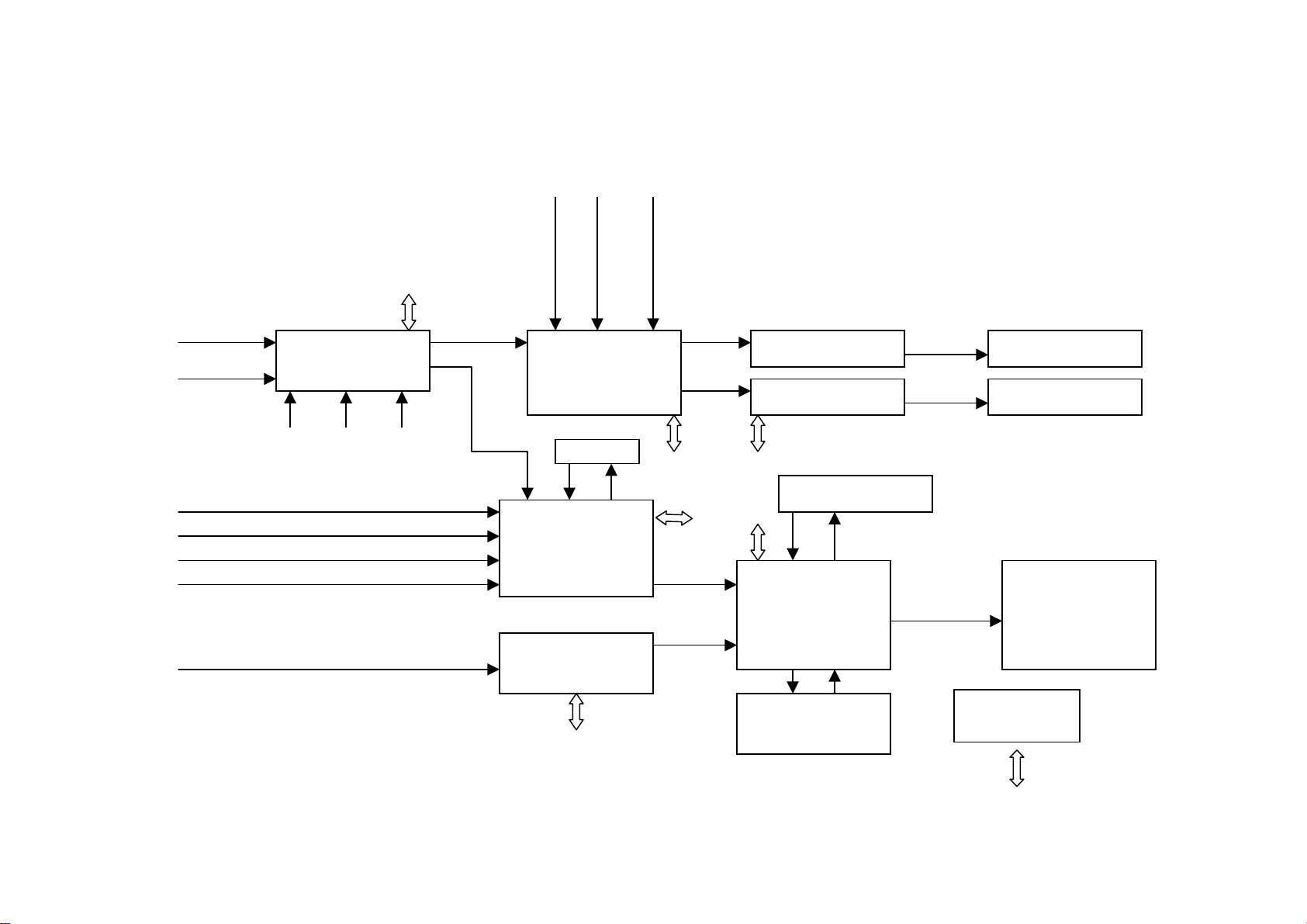
3. IC function, the internal block diagram, the pin introduction
3.1 PW2300
PW2300 is a piece of the front-end video-processing chip that integrates a high-powered,
multi-system video decoder with a high speech ADC module. All of the input video signal (except for
HDMI signal) are inputted to this chip to the AD switch and video decoding, 24 bit digital RGB signal
9
Page 12
and the related sync signal are outputted to N602 PW118 to make the processing. PW2300
complete mainly the functions of 3D comb filter, the channel switch, 5-line Y/C separation, the color
decoding and so on. It connect external SDRAM chip N703 HY57V161610E treated as the internal
memory to assist the operation of PW2300.
PW2300 internal block diagram:
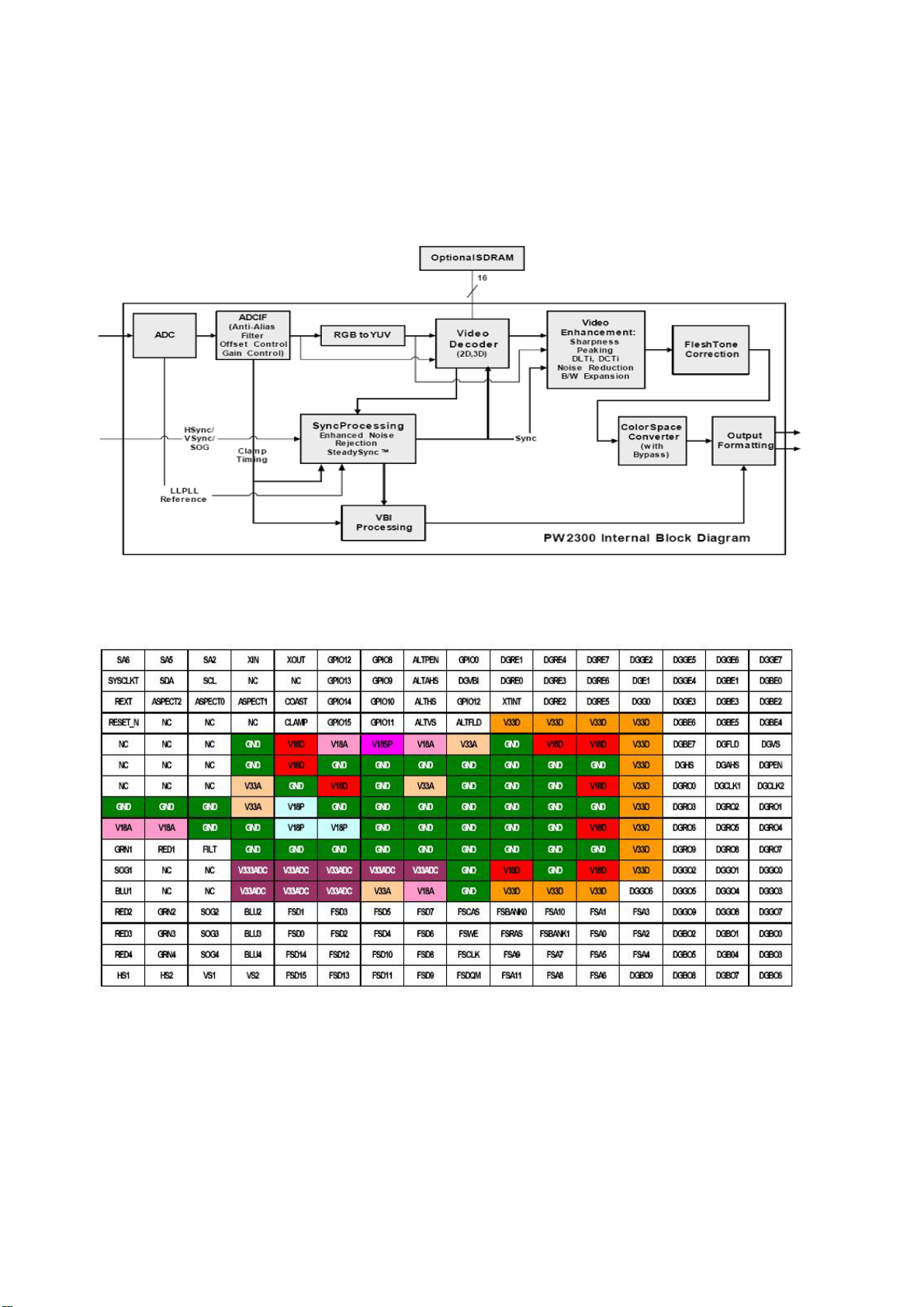
PW2300 the arrangement diagram of the pins:
10
Page 13

PW2300 instruction of the pin:
Pin Name Function Pin Name Function
A4 XIN Resonator input N4 B_1 AV1 blue input
A5 XOUT Resonator output P1 R_2 AV2 red input
B2 SDA I2C bus data P2 B_2 AV2 green input
B3 SCL I2C bus clock R3 CVBS_SOG1 T multiple green sync output
of video signal
K2 VGA-R1 VGA red R4 C_1 S-VHS color signal input
K1 VGA-G1 VGA green B9 GVBI Vertical blanking interval
M1 VGA-B1 VGA blue E16 G_VS Vertical sync output
T1 VGA_H VGA CH1 horizontal
sync
T3 VGA_V VGA CH1 vertical sync F15 G_AHS Crude horizontal sync
N1 R_1 AV1 red input G15 G_DLK Clock output
N1 G_1 AV1 green input B10-B12
P3 SOG_2 AV2 green sync input C13,
P4 G_2 AV2 blue input B15-B16
F14 G_HS Horizontal sync output
GRE (0-7) Red data output
A10-A12
C11-C12
GGE (0-7) Green data output
C14
B13,
B14
A13-A16
C15-C16
E14
GBE (0-7)
Blue data output
3.2 AD9398
The chip of high-definition multimedia interface, AD9398 HDMI (High-D efinition Multimedia
Interface) this interface is the digital interface standard that bring up rapidly. The use of this
interface is the transmission of electronic video signal of standard definition and high definition, and
this interface provide the content protect technology. AD9398 also support HDCP (High bandwidth
Digital Content Protection). AD9398 include a HDMI 1.0 interface module and a HDCP module. The
inputted HDMI signal will be sent to the interface of this chip to make the decoding, simultaneity
24-bit digital RGB signal and the related sync signals are outputted to N602 PW118 to make the
processing. Moreover, HDCP module makes the communication by DDCSDA, DDCSCL and HDMI
signal sources to make the video signal decoding. The chip connect a external memory N207
24LC168SN that store the secret key of decoding required by HDCP, and make the communication
by the pin MCL, MDA of AD9893.
11
Page 14

AD9880 (AD9398) internal block diagram:
AD9880 (AD9398) instruction of the pin:
Pin Name Function Pin Name Function
2-9 GGE(0-7) Switch output 44 RXC+ DVI digital video input
12-19 GBE(0-7) Switch output 49 DDC_CLK HDCP (serial data clock)
92-99 GRE(0-7) Switch output 50 DDC_DATA HDCP (serial data I/O)
20, 21 MCLK Control clock output 51 MCL HDCP control series data
clock
22 I2S_SCK Audio series clock output 52 MDA HDCP control series data
I/O
23 I2S_WS Bus clock data output 82 SCL-1 Series data clock
27 I2S_SD Bus audio data output 83 SDA_1 Series data I/O
34 RX0- DVI digital video input 84 G_FIEL0 Parity field output
35 RX0+ DVI digital video input 85 G_VS Vertical data sync output
37 RX1- DVI digital video input 86 G_VHS Green sync output
12
Page 15

The arrangement diagram of the pins:
3.3 PW118
PW118 is the new high-powered image manipulation chip of Pixelworks. The 24 bit digital RGB
signal and the related sync signal outputted by AD9398 and PW2300 shall be inputted to this chip to
make the image manipulation, and are outputted LVDS signal to drive the screen directly. In
addition to the function of interlaced to line-by-line, this chip further include the function of image
enhancement, etc. This chip is the main CPU of this set. It take charge of all control except for the
power supply control, including the control of each chip operation in the main board (eg. the image
manipulation, the channel switch, the image display, etc.), the control of the button, remote device
and sound, etc., and the assistant CPU N401 ATMEGA8L control mainly the power supply,
including the stand-by and the control button of remote device to turn on the set, etc. The menu
interface also generate by PW118. The external memory of PW118 N402 AT24LC32A stores the
related data. The Flash chip N404 MX29LV800 store the related procedure, the chip DDRSDRAM
(N501 K4D553238F-JC) assists the operation of PW118 as the external memory.
13
Page 16

PW118 internal block diagram:
The arrangement diagram of the pins:
3.4 M52797
M52797 is a AV switch chip controlled by IIC. This chip include 4 group of video input and 4 group of
audio input, 2 video output and 1 audio output.
14
Page 17

M52797 Internal block diagram:
The arrangement diagram of the pins:
15
Page 18

M52797 instruction of the pin:
Pin Function Pin Function
3 YPbPr2_L audio input 20 Video output to PW2300
5 YPbPr2_R audio input 22 Right track audio output
6 AV1_L audio input 23 Video output to AVOUT interface
7 AV1 audio input 24 Left track audio output
8 AV1_R audio input 25 TV_R audio input
9 AV2_L audio input 26 TV video input
10 AV2 audio input 27 TV_L audio input
11 AV2_R audio input
3.5 R2S15900
R2S15900 is a audio processing chip that take charge of audio switch, sound processing and
volume adjustment, controlled by IIC bus.
Internal block diagram:
16
Page 19

R2S15900 instruction of the pin:
Pin Function Pin Function
2, 27 Left and right track of M52797 5, 24 Left and right track of YPbPr1
3, 26 Left and right track of HDMI 11, 19 Left and right track of audio output
4, 25 Left and right track of VGA
3.6 LA72700 (STEREO/SAP DECODER):
PIN description:
Pin No. Name Description Pin No. Name Description
5 PISIF Audio IF input 25 R OUT Right channel audio output
11 SDA I2C bus 26 LOUT Left channel audio output
12 SCL I2C clock 31 VCC 9V
17
Page 20

Diagnose and service of panel
1. Block function of panel
The power supply board, Logic board, X drive board, Y drives board, Logic BUFFER (E, F and G)
and Y BUFFER (upper and lower) of the PDP panel.
Y BUFFER (upper)
Y BUFFER (lower)
Logic BUFFER (E)
Logic BUFFER(F) Logic BUFFER(G)
Power supply board
X drive board Y drive board
Logic board
COF(7 piece)
* Power supply board: to supply power for the screen, other functional modules on the screen, our
own main board, and video frequency processing board.
* X driving board: to produce and provide driving signal for X electrode according to the time
sequence signal sent from logic board.
* Y driving board: to produce and provide driving signal for Y electrode according to the time
sequence signal sent from logic board.
*Logic board: to process the image signal sent from the main board, to produce addressing signal
and to provide driving signal for X and Y driving boards.
*Logic BUFFER board: To convert the data signal and control signal sent from the logic board into
the signals required by COF.
*Y BUFFER board: to transmit the scanning signal from the Y driving board to the screen, which is
divided into upper and lower parts.
*COF: to convert the signal sent from the logic BUFFER board into the address signal used by the
screen.
2.Trouble diagnosis:
2.1 The screen is not bright:
a. Check if the power supply plug from the power filters board to the power supply board is well
inserted into the socket. If not, plug it in.
b. Check if the fuse on the power supply board is blown up. If yes, replace it for a good one.
c. Remove our main board and the video frequency processing board, ground the pin 4
18
Page 21

POWER_ON/OFF of socket CN802 of the power supply board;
SW200
Solder point
and then push the slide switch SW2001 on the logic board to the internal modes (1, 3 up and 2, 4
down) from external modes (1, 2, 4 up and 3down).
1
Switch the power on and see if the screen is lit. If the screen can give a normal and completely
white field signal, then the problem lies in our main board or video frequency processing board,
which will be dealt with separately.
d. If the screen is not lit, then first replace the power supply board to see if the problem is solved.
e. If the problem remains after the power supply board is replaced, then the problem lies in the
screen, replace the entire screen for treatment.
2.2 There appears on the screen a line or several unlit lines.
Check if the socket between Y driving board and Y BUFFER is plugged well. If not, plug it well. If
19
Page 22

yes then replace Y BUFFER (upper, lower) in respect to the upper, lower part of the dark line on the
screen.
2.3 There appear on the screen one or several horizontal lines that are much brighter than the
remaining horizontal lines at the edge:
Check if the socket between Y driving board and Y BUFFER is plugged well. If not, plug it well. If
yes then replace Y BUFFER (upper, lower) in respect to the upper, lower part of the dark line on the
screen.
4.There appear on the screen one vertical unlit line or a vertical entirely unlit block
a. If it’s one vertical unlit line, then COF has problem.
b. If it’s a vertical entirely unlit block, then first check if the connection socket between COF and
logic BUFFER has problem. If not, check if the connection sockets between the logic BUFFER and
the logic board is normal. If yes, replace the logic BUFFER. Finally, if the problem still remains when
the replacement is over, then replace the logic board.
5.There appears on the screen a mono color signal and one or several vertical bright lines of other
colors:
a. If it’s a vertical bright line of other colors, then the problem lies with COF or the screen.
b. If it’s an entire vertical block of other colors, then first check to see if the connection socket
between COF and logic BUFFER has problem. If no problem, check if the connection socket
between the logic BUFFER and the logic board is normal. If it’s normal, then replace the logic
BUFFER. If the problem still remains after the replacement, then replace the logic board. Finally if
the problem is still there, then the problem lies with COF.
6.There appear on the screen abnormal bright spots or blocks that are different from what’s
described above:
a. Check if the connection socket between COF and logic BUFFER board has been well plugged.
b. Replace the logic BUFFER board. If it’s not solved then replace logic board. If the problem still
remains, then it’s the problem with COF.
20
Page 23

Wiring Diagram
Logic board
LA03
31 7 11 10 4
`
X600 X400 X405
Panel
Power supply filter board
2
Power supply board
CN9004 CN9003 CN8001
Speaker assembly
X909 X908
button board
Data processing board
RS-232 HDMI VGA
YPbPr/YCbCr1 YPbPr/YCbCr2
21
X301 X300 X302
X904 X903 X906
HF board
6 12 9
AV out
S-Vide o in
AV1 in AV2 in
earphone
RF
Page 24

Assembly list
Parts No. (203-PH50T180-03) Description
SPH50T180-03A10 Software PW118
SPS42T60-01B10 Software MEGA8
SPS42T60-01C10 Software HDMI EDID
SPS42T60-01D10 Software VGA EDID
301-IL37T25-04 RC-I04 remote control
535-DZ2850-01 Panel stand assembly (DZ-2850)
535-PH50D8-05 Mounting assembly
615-20513-AW0 Speaker assembly
667-PSIT6-55A High frequency board
667-PH50T18-69 Digital processing board
667-PH50T18-51 Supply power filter board
667-PH50T18-05 Buttons board
667-PH50T18-14 Indicator light assembly
335-50003-00 Display screen (PDP50X3-4004)
22
Page 25

Trouble shooting guide
b
b
f
p
y
p
f
N
N
N
N
1.No raster, no picture, no sound
No raster, no picture, no sound.
Measure the level of 8th pin of X405:
when use V4 screen, it should be low
level; when use V7 screen, it should
be high level.
ormal Abnormal
Check the level
of power suppl
in of each IC.
Check power supply
D3.3V, D5V
Abnormal
Check N401
NOTICE: The PDP power supply have the protection function of overcurrent, overvoltage
and so on, if certain route power supply appear overcurrent and overvoltage, the power
supply should appear the protection to arise no-output.
Check if the power supply indicator light is on.
yes
ormal
Check if the
union joint o
602 and LVDS
line is loose.
no
Cut off the connection
etween power supply
oard and data board, and
test 5V-STBY
Abnormal
Check N401
and keyboard.
Check 5V-STBY
ormal
The problem o
ower supplies
board.
23
Page 26

2.With sound but no picture:
p
N
d
t
f
p
t
NoN
N
N
N
Check if all other channel
has no
and periphery
circuit
icture.
o
602 PW118
Turn to check 4
of program
With sound but no picture.
Display logo?
Ye s
Check if the G401 an
Ye s
ormal
N602 damaged.
G7000 have the signal
wave.
Abnormal
Check the input signal of N602
and
ower supply.
ormal
Check N700
and the circui
of output.
Unfix X405 and X406, shor
circuit the PIN8 of X405 to GND,
set switch of the logic board as
self-testing signal, then check i
display the white screen.
ormal Abnormal
The screen damaged.
Abnormal
Set self-testing of the screen:
a. 42” SD screen: Push down 2 and 4 and push up 3 of SW2001 on the logic board;
b. 50” HD screen: Push down 1 and 4 and push up 2, 3, 5, and 6 of SW2001 on the logic board;
c. Please make sure resume it to the original status when the check is over.
24
Page 27

3.With picture but no sound:
r
p
d
p
p
f
N
N
N
t
p
N
p
N
N
N
If the sound power board X908 is output.
Check if the second pin of soun
ower amplifier input the signal.
The sound power amplifier or peripheral
circuit has problem. Check power supply,
if the control of SHUTDOWN pin is
normal; if output short-circuited or othe
roblems that cause protection to work.
4. A certain channel is abnormal
4.1 No picture on AV
Check N602 and
eriphery circuit
Check if TV channel is
normal.
Ye s
o Yes
The sound damaged.
oYe s
Measure if the sound
input of current channel
of N907 is normal.
oYe s
Check N907 or
eripheral circuits.
Check different levels o
circuit following input audio
signal channel.
Measure if the AV inpu
in of N700 have the
signal input.
oYe s
Check N903 M52797
and periphery
o
Check if N700
output is normal.
Ye s
o
700 is damaged
25
Page 28

4.2 YPrPb or YCrCb no picture
p
n
d
p
No N
f
N
N
d
p
N
N
N
Check if the YPRYPB input pi
of N700 have signal.
Check N700 an
4.3 TV no picture
700 damaged
Check if AV channel
is normal.
ormal Abnormal
o Yes
Check if YPRPB1 / YCRCB1 and YPRPB2
/YCRCB2 channels is no
Ye s
Ye s
eriphery circuit
Check if the input signal o
700 is normal.
ormal
Check if N700 has
output.
o
icture.
check interface
circuit.
Abnormal
Check N602 an
Check N903
M52797 and the
tuner.
eriphery circuit
26
Page 29

4.4 VGA no picture
p
d
p
t
N
N
Check the horizontal and vertical sync
signal of HS1 and VS1 input of N700.
ormal
Check N700 an
eriphery circuit
Check if the input YPRPB
signal is normal.
o Ye s
Check N700 and
eriphery circuit
Abnormal
The matter of inpu
interface circuit, N211
and periphery circuit
4.5 HDMI no picture
If no picture, check firstly if the set of external device is normal, after eliminating the device problem
still no picture, check X200, N208 and periphery circuit.
4.5.1 Abnormal of the picture:
a. A certain differential wire pair of LVDS (RX0+/-, RX1+/-, RX2+/-, RX3+/-) of X600 is abnormal,
which may lead to lack of color (it’s not a complete loss of color).
b. Failure with resistor rows R606~R610, which may lead to loss of corresponding color from the
gray degree corresponding to the picture of all channels.
c. Failure with resistor rows R708~R713, which may lead to loss of corresponding color from the
gray degree corresponding to the picture of VGA/YPRPB/AV/TV channels.
d. Failure with resistor rows R258~R263, which may lead to loss of corresponding color from the
gray degree corresponding to the picture of HDMI channel.
4.5.2 Abnormal picture vertically or horizontally (bar like): Abnormal in complete line extending all
the way from up downward on the screen of stand definition TV set; abnormal vertically on half
screen of high definition TV set. They may be caused by the damage of the address BUFFER
module that directly corresponds to its position, or may be caused by the damage of the connection
wire that directly corresponds to the position of the screen. The horizontal bar like abnormality is
also related to the Y driving circuit that corresponds directly to its position. To judge these
phenomena, It’s possible to check it by setting the screen to the status of self check as explained
above
4.5.3 No brightness in the square block area: Normally it’s caused by the damage of the address
BUFFER module that directly corresponds to its position, or may be caused by the damage of the
connection wire that directly corresponds to the position of the screen. To judge these phenomena,
it’s possible to check it by setting the screen to the state of self-check as explained above.
27
Page 30

Digital board
Page 31

Digital board
Page 32

Digital board
Page 33

Digital board
Page 34

Digital board
Page 35

Digital board
Page 36

Digital board
Page 37

Digital board
Page 38

High frequency
board
Page 39

Key board
Page 40

603-PH50T180-03
Ver.1.0
 Loading...