

Page 1

PDP TELEVISION
PH-42R6
Canada
Page 2

CONTENTS
Safety precautions………………………………………………………………………..…
Alignment instructions …………………………….…….……………………………….…
Working principle analysis of the unit……………………………….………….………….
Block diagram…………………………………..………………………………….…………
IC block diagram………………………………………………………………………..……
Wiring diagram ……………………………………………………………..……………...
Troubleshooting………………………………………………………………………..……
Schematic diagram …………………………………………………………………………
APPENDIX-A: Main assembly list
APPENDIX-B: Exploded view
1
3
6
7
8
17
18
24
Page 3

Note: This maintenance manual is intended only for the reference of the maintenance people.
Please pay attention to the following points before carrying out the maintenance work.
Safety precautions
Please read the “Points for attention for the Maintenance & Repair of PDP” and “Criterion for
Identifying the Defects on Screen” as below, before inspecting and adjusting the TV set.
1. “Points for attention for the Maintenance & Repair of PDP”
To avoid possible danger, damage or jeopardy to health and to prevent PDP screen from new
damage, the maintenance people must read the following carefully. If they ignore the following
warnings, there will be deathful risks:
1.1 Screens vary from one model to another and therefore not interchangeable. Be sure to use the
same type of screen in the replacement.
1.2 The operation voltage is approximately 350V for PDP module (including screen, driving circuit,
logic circuit and power module). If you want to conduct maintenance work on PDP module when the
set is in normal operation or just after the power is off, you must take proper measures to avoid
electric shock and never have direct contact or touch with the circuitry of the working module or
metal parts. That’s because within a short time relatively high voltage still remains on the capacitor
of the driving part even after the power is off. Make sure to begin relevant maintenance operation at
least one minute after the power is off.
1.3 Don’t apply on the module any power supply that is higher than the specification. If the power
supply used deviates from the value given in the specification, there might be a possibility of leading
to fire or damage to the module.
1.4 Never have operation or mounting work under unsuitable environment such as areas in the
vicinity of water – bathroom, laundry, water chute of kitchen – sources of fire, heat-radiation parts or
direct exposure to sunlight. Otherwise there will be kickbacks.
1.5 In case foreign substances such as water, liquid, metal slices or others fall into the module
carelessly power must be cut off immediately. Keep the module as it is and do not move anything on
the module. Otherwise it might be possible to contact the high voltage or cause shock short circuit
so that it may lead to fire or electric shock.
1.6 If there is smoke, abnormal smell or sound from the module, please cut the power off
immediately. Likewise in case the screen doesn’t work when the power is on or during the operation,
please also cut off the power at once. No more operation in this case.
1.7 Do not remove or plug its connection wire when the module is in operation or right after the
power is off. That’s because there remains a relatively high voltage on the capacitor of the driving
circuit. If there is a need to remove or plug in the connection wire, please wait at least one minute
after the power is off.
1.8 Considering the module has a glass faceplate, please avoid extrusion by external force lest it
should cause glass breakage that may get people injured. Two people are needed in cooperation to
move this module lest contingency takes place.
1.9 The complete TV set is designed on the basis of full consideration of thermal dissipation by
convection, with the round hole on the top for heat emission. To avoid overheat, please do not have
any covering on the hole during normal operation and never put it in the place where the space is
narrow and in bad ventilation.
1.10 There is quite a number of circuits in PDP that are integrated ones. Please be on guard against
1
Page 4
static electricity. During maintenance operation be sure to cover yourself with anti-static bag and
before operation make sure to have it sufficiently grounded.
1.11 There are a big number of connection wires distributed around the screen. Please take care
not to touch or scuff them during maintenance or removing the screen, because once they are
damaged the screen will fail to work and it’s not possible to repair it.
1.12 Connector for the circuit board of the screen part is relatively fine and delicate. Please take
care in the replacement operation lest it should get damaged.
1.13 Special care must be taken during transportation and handling because strenuous vibration
could lead to screen glass breakage or damage on the driving circuitry. Be sure to use a strong
outer case to pack it up before transportation or handling.
1.14 Please put it for storage in an environment in which the conditions are under control so as to
prevent the temperature and humidity from exceeding the scope stipulated in the specification. For
prolonged storage please cover it with anti-moisture bag and have them piled and stored in one
place. The environmental conditions are tabulated as below:
Temperature Scope for operation 0~50centigrade
Scope for storage -15~60centigrade
Humidity Scope for operation 20%~80%
Scope for storage 20%~80%
1.15 If a fixed picture is displayed for a long time, difference in its brightness and color may occur
compared with movable pictures. But it doesn’t show any problem and the reason is that there is
reduced density of fluorescent powder in the former. On the other hand, even if changes take place
in the picture, it can keep its brightness for a period of time (several minutes). It’s a feature inherent
with plasma and it’s not abnormal. However please try as much as possible to avoid showing a still
picture of high brightness for a long time during operation.
1.16 As a digitalized display devise, this module is provided with error diffusion technology and the
gray scale and false enhancement of contour can be displayed by reusing of sub-field. As compared
with cathode ray tube, it can be found in the moving picture that at the brim of the face of a person
there are some wrong colors.
1.17 During the display of graph (indicating the gradual change in brightness horizontally or
vertically) resulting from gray scale test it can be found that the brightness for the two adjacent
levels is uneven. This is caused by the reuse of sub-field, the display of load rectification and the
electrolysis.
1.18 The screen front plate is of glass. Please make sure that the screen has been put in place
during erection. If it is not in place before the erection begins it may lead to screen crack or
breakage.
1.19 Make sure the screw used in the mounting of the screen is of the original specs lest it should
cause damage to the screen due to mismatch. Special care should be taken not to use too long or
too big screw.
1.20 Care must be taken to guard against dust during assembling or dismantling, especially to avoid
dirt from falling in between the screen and the glass lest it should harm the receiving and viewing
effect.
1.21 There is piece of insulator stuck on the rear chassis corresponding to the power supply board.
It is used to isolate the cool part from the hot part. Please take care to keep it intact lest it should
2
Page 5
become a potential safety trouble.
1.22 In addition to plasma screen, the glass is a part of high value. It has such functions as
anti-radiation, adjustment of color temperature etc. Please handle it carefully.
Alignment instructions
1. Test equipment
VG-848 (Signal generator)
CA100 (White balancer)
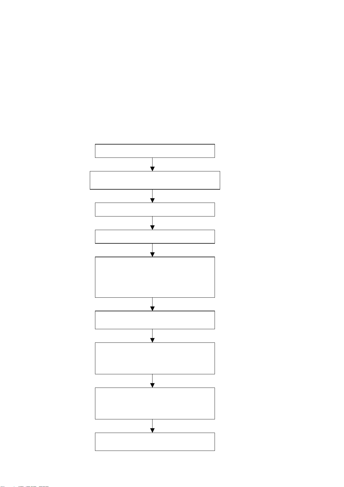
2. The alignment flow chart (see below figure)
Production of CPU board and analog board on the line.
Check DDC, HDCP KEY and FLASH
Check CPU board and analog board
Combined test for general assembly
Connect to central signal source; check if various
TV functions (station skipping, modulate quantity
control etc), check if the output of earphone and
speaker are normal.
Input AV/S signal and HDTV signal; check various
functions under AV/S terminal
Input VGA signal and check if display is normal in
the state of PC and various functions (analog
quantity control, line/field center etc.)
Input HDMI signal and check if display is normal in
the state of HDMI and various functions (sound
and analog quantity control).
Preset ex-factory
3
Page 6
Check accessories and then packing
Fig-1 adjustment flow-chart
3. The unit adjustment
Connect all the boards according the wiring diagram, turn on the power and check if the display is
normal.
3.1 The method of entering factory menu
Enter factory menu method: press the INPUT→ 2→ 5→8→0 buttons one by one on the remote
control to factory menu. Press the MENU button to select item. Press the DISPLAY button to exit the
factory menu.
3.2 EEPROM initialization and back light adjustment
Enter the firs page of factory menu, adjust item OPTION-1 to 9, OPTION-2 to 5, select the
EEPROM initial after, press the VOL+ button, then display the DOING, still the DOING disappear
and turn off the unit.
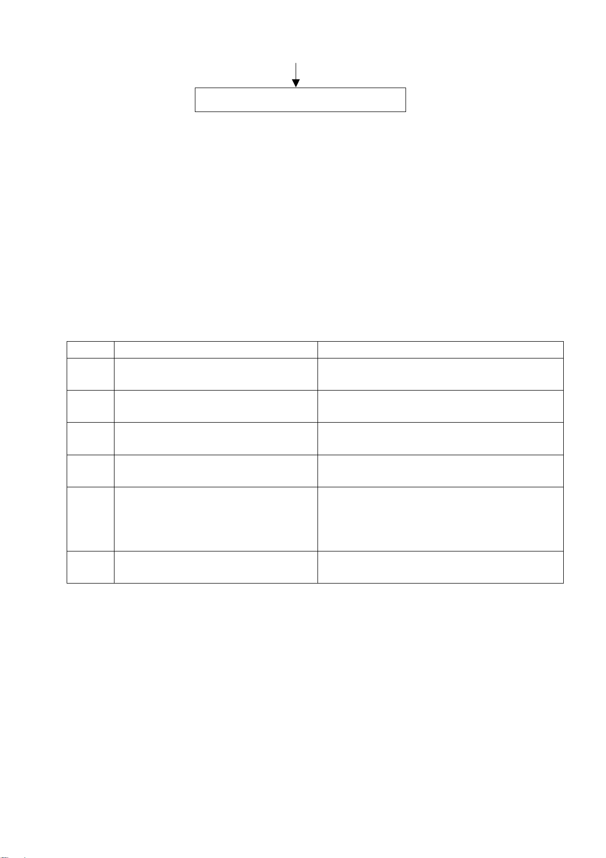
Note: option-1 and option-2 function as follows:
Option-1 Option-2
Bit6 0: normal TV mode
1: hotel TV mode
Bit5 0: TV/AV multi-system
1: TV/AV NTSC system
Bit4 0:fast search station
1:slow search station
Bit3 0: no memory function after power off for 10s
1: memory function after power off for 10s
Bit2,1 00: STANDBY
01: turn on
10: memory function of turn on
Bit0 0: without LOGO
1: With LOGO
3.3 HDMI channel adjustment
Input the VG-848 TIME854(800X600/60Hz) and PATTERN920 8-LEVEL gray signal, enter the
factory menu2(white balance adjustment menu), adjust the second step and the seventh step.
Adjust R-OFFSET, G-OFFSET and B-OFFSET item, still the second step color coordinate to (285,
293). Adjust R-GAIN, G-GAIN and B-GAIN item, still the seventh step color coordinate to (285, 293).
Repeat adjustment R-OFFSET, G-OFFSET and B-OFFSET item and R-GAIN, G-GAIN and B-GAIN
item, still two step gray to (285, 293).
Note: R-OFFSET, G-OFFSET and B-OFFSET values must be an item value to 128 at least; R-GAIN,
G-GAIN and B-GAIN values must be an item value to 255 at least.
3.4 VGA channel adjustment
3.4.1 mode pre-set
Input the VGA signal of VG-848 (PATTERN 980:1 dot ON/OFF), select the TIME877 (720x400/70Hz)
0:close HDMI hot-plug function
1:open HDMI hot-plug function
0:only have the first two pages of factory menu
1:all pages of factory menu
0:have GAMMA correction
1:no GAMMA correction
0:no signal noise wave of TV
1:no signal blue screen of TV
00:complexion correction (OFF)
01: complexion correction (WEAK)
10: complexion correction (MIDDLE)
11: complexion correction (STRONG)
0: Video and Graphic channel white balance no share
1: Video and Graphic channel white balance share
4
Page 7

signal, press auto-adjust button to all screen or adjust PC settings menu to auto correction.
Separate auto adjust for TIME885 (640x480/60Hz) and TIME854 (800x600/60Hz).
3.4.2 VGA channel auto color adjustment
Input the VG-848 TIME854(800x600/60Hz) and PATTERN920(GRAY 8 STEP(H)), enter the factory
menu1, select the AUTO COLOR after, press the VOL+ button to select AUTO COLOR.
3.5 HDTV channel adjustment
Input the VG-848 TIME972(1080i/60Hz) and PATTERN976(64 GRAY & Color), enter the factory
menu1, select the AUTO COLOR after, press the VOL+ button to select AUTO COLOR.
4. Performance check
4.1 TV function
Input center source signal to RF-TV terminal, check if the channel is leak for auto searching.
4.2 AV/S and HDTV terminal
Input AV/S and HDTV signal, check if the signal is normal.
4.3 VGA terminal
Input 640 x 480 @60Hz VGA format signal, check if the signal is normal.
4.4 HDMI terminal
Separate input HDMI and DVI signal; check the picture and sound is normal, check if the HDCP
function is normal.
4.5 check the sound channel
Check the speaker and headphone of each channel.
4.6 ex-factory setting
Enter the first page of factory menu, select the factory out after, press the VOL+ button to display
“doing”, then “doing” disappear while it can auto ex-factory setting.
5
Page 8

Working principle analysis of the unit
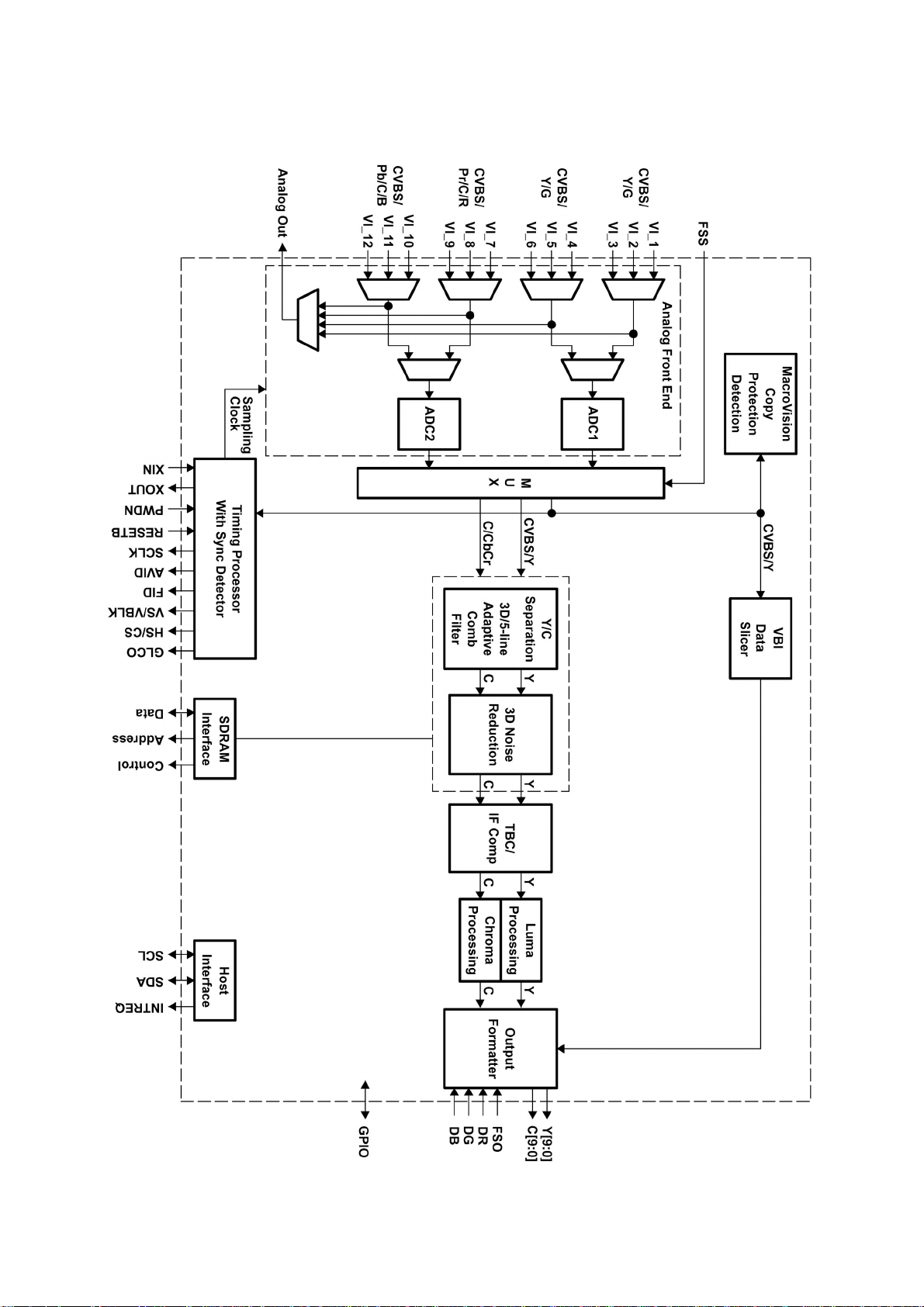
The RF1 via integrative tuner TUNER1 after, the FBAS VIDEO1 and SIF1 is generated. Video
signal of VIDEO1, AV1/S, AV2 sent to N7(TVP5160) as the main picture signal. The signal via N7
switch selection after, one way is AV OUT; another way sent 8-bit ITU-R656 format signal to N10
(FLI2310) non-interlaced processing, then sent 24bit YUV signal to main processing control chip
N15 (GM1501/1601).
The RF2 via integrative tuner TUNER2 after, the FBAS VIDEO2 and SIF2 is generated. Video
signal of VIDEO2,AV1/S,AV2 sent N8 (TVP5147) to decode as sub-picture signal. The signal via N8
decode after, it sent 8-bit ITU-R656 format signal to main processing control chip N15
(GM1501/1601).
Two ways YPBPR signal via HDTV switch N39(PI5V330) selection after, it sent to RGB switch
device N4(PI5V330) switch selection with RGB signal from VGA interface, then it sent to
GM1501/1601.
The HDMI via receiver N34(MST3383MB) processing after, it output RGB signal of 24bit to
GM1501/1601.
They sent to GM1501/1601 picture processing, therein YPBPB or RGB to A/D conversion after, it
and other three signal are switched selection and digital display processing, it include OSD,
GAMMA correction, brightness and contrast processing, then LVDS conversion to PDP panel
display.
The SIF1 of tuner1, SIF2 of tuner2 and audio signal of AV1/S, AV2 separate sent to audio processor
NA3(MSP3420).
The HDMI via chip N34(MST3383MB) decode to digital audio, after N26(CS4334) D/A conversion, it
audio and the audio signal of VGA/DVI sent to N44(HEF4052) switch selection, then sent to
MSP3420.
The audio of two YPBPR and VGA via switch conversion N42(HEF4052) to MSP3420 too.
The stereo of the SIF1 and SIF2 with other four ways audio switch conversion selection to volume
control and audio processing. One way output right/left channel audio of main-picture, the signal
sent SRS processing NA5 (M62494) to SRS sound stereo processing. It via sound amplifier
NA6(MP7722) to speaker; one way output right/left channel audio of sub-picture, it sent to earphone,
another way is AV OUT R/L output.
The work of whole unit is controlled by MCU, which includes GM1501/1601.
6
Page 9
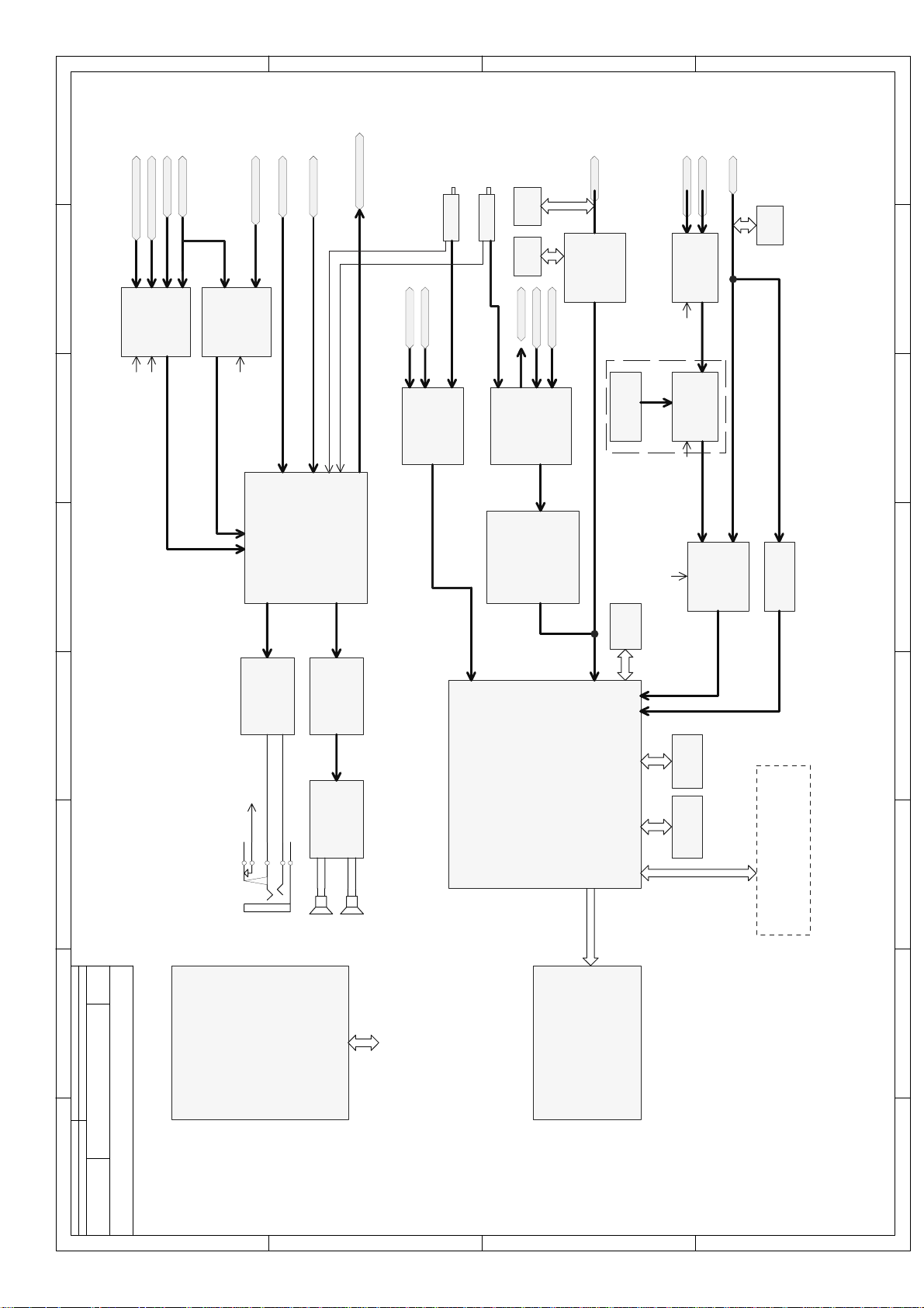
A
Block diagarm
B
C
D
1 2 3 4 5 6 78
L/R_VGA
L/R_YPbPr1
L/R_YPbPr2
N42
YUV_SW
TC4052
YUV/USB
L/R_USB
Audio Switch
N44
TC4052
L/R_HDMI
L/R_AV1
L/R_AV2
Audio Switch
VGA/HDMI_SW
SIF
ANA_IN1
SC2_L/R
SC1_L/R
ANA_IN2
Audio Processor
MSP3420G
SC3_L/R
SC4_L/R
SC2_OUT
NA3
DACM_L/R
AUDIO OUT
HDMI
EDID
24C02
Tuner 1
Tuner 2
HDCP KEY
24C04
AV IN 1
AV IN 1
AV IN 2
AV IN 2
V OUT
MST3383
N34
HDMI RX
N39
YPbPr 2
CBT3257C
VGA
YPbPr 1
EDID
24C02
HDTV Switch
YUV_SW
OPTION
Media Player
N7
N10
TVP5160
FLI2310
Video Decoder
Deinterlacer
(USB)
Video Decoder
TVP5147
N8
SC1_OUT
CBT3257C
YUV/USB
YUV/VGA
HDTV Switch
Y Pb/Cb Pr/Cr
CBT3257C
RGB Switch
R G B
Hs Vs
SN74AHC14
N4
TDA7053AT
Head Phone
AMP
HP_SW
NA7
M62494FP
NA5SRS
Audio AMP
MP7722
NA5
NA6
N15
GM1601/GM1501
EEPROM
LCD TV Controller
Y Pb/Cb Pr/Cr
R G B
Hs Vs
Frash/ROM
Power_ON,IR,KeyA,KeyB,Led1,Led2
Mute,HP_SW,VGA_CAB,DVI_CAB
YUV/VGA,YUV_SW,YUV/USB
Frame Buffer
DDR
Title
SizeA3Date: 19-May-2006
File: G:\ \..\PH42R6BLOCK.Sch
Number
邱杰的文件 Drawn By:
PH42R6 BLOCK DIAGRAM
Power Supply
Power_ON,+5V_STB,VCC,VBL
PANEL
7654321
Sheet of
Revision
Ver 1.0
yyc
A
B
C
D
8
7
Page 10

IC block diagram
1.MSP3420
The MSP 34x0G family of single-chip Multistandard Sound Processors covers the sound
processing of all analog TV-Standards worldwide, as well as the NICAM digital sound standards.
The full TV sound processing, starting with analog sound IF signal-in, down to processed analog
AF-out, is performed on a single chip. Figure 1–1 shows a simplified functional block diagram of the
MSP 34x0G.
This new generation of TV sound processing ICs now includes versions for processing the
multichannel television sound (MTS) signal conforming to the standard recommended by the
Broadcast Television Systems Committee (BTSC). The DBX noise reduction, or alternatively,
Micronas Noise Reduction (MNR) is performed alignment free.
Other processed standards are the Japanese FM-FM multiplex standard (EIA-J) and the FM Stereo
Radio standard.
Current ICs have to perform adjustment procedures in order to achieve good stereo separation for
BTSC and EIA-J. The MSP 34x0G has optimum stereo performance without any adjustments.
All MSP 34xxG versions are pin compatible to the MSP 34xxD. Only minor modifications are
necessary to adapt a MSP34xxD controlling software to the MSP 34xxG. The MSP 34x0G further
simplifies controlling software. Standard selection requires a single I2C transmission only.
The MSP 34x0G has built-in automatic functions: The IC is able to detect the actual sound standard
automatically (Automatic Standard Detection). Furthermore, pilot levels and identification signals
can be evaluated internally with subsequent switching between mono/ stereo/bilingual; no I2C
interaction is necessary (Automatic Sound Selection).
The MSP 34x0G can handle very high FM deviations even in conjunction with NICAM processing.
This is especially important for the introduction of NICAM in China.
The ICs are produced in submicron CMOS technology. The MSP 34x0G is available in the following
packages: PLCC68 (not intended for new design), PSDIP64, PSDIP52, PQFP80, and PLQFP64.
8
Page 11
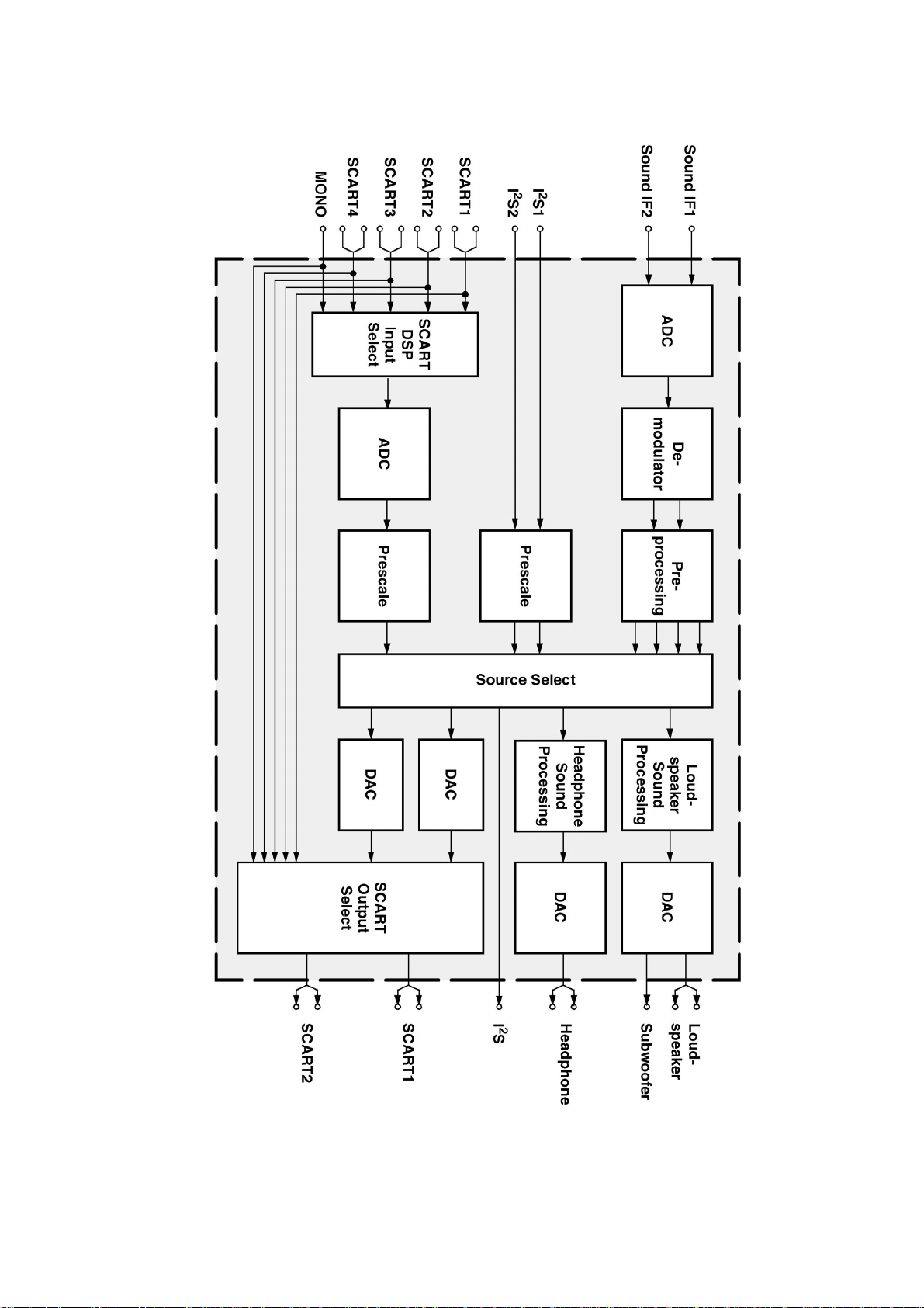
Fig. 1–1: Simplified functional block diagram of the MSP 34x0G
9
Page 12

2. TVP5160
The TVP5160 device is a high quality; digital video decoder that digitizes and decodes all popular
baseband analog video formats into digital component video. The TVP5160 decoder supports the
A/D conversion of component YPbPr and RGB (SCART) signals, as well as the A/D conversion and
decoding of NTSC, PAL, and SECAM composite and S-Video into component YCbCr. Additionally,
component progressive signals can be digitized. The chip includes two 11-bit, 60-MSPS, A/D
converters (ADCs). Prior to each ADC, each analog channel contains an analog circuit, which
clamps the input to a reference voltage and applies a programmable gain and offset. A total of 12
video input terminals can be configured to a combination of YPbPr, RGB, CVBS,and S-Video video
inputs.
Progressive component signals are sampled at 2x clock frequency (54 MHz) and are then
decimated to the 1x rate. In SCART mode the component inputs and the CVBS inputs are sampled
at 54 MHz alternately, then decimated to the 1x rate. Composite or S-Video signals are sampled at
4x the ITU-R BT.601 clock frequency (54 MHz), line-locked for correct pixel alignment, and are then
decimated to the 1x rate. CVBS decoding utilizes advanced 3D Y/C filtering and 2-dimensional
complementary 5-line adaptive comb filtering for both the luma and chroma data paths to reduce
both cross-luma and cross-chroma artifacts. 3D Y/C color separation may be used on both PAL and
NTSC video signals. A chroma trap filter is also available. On CVBS and Y/C inputs, the user can
control video characteristics such as hue, contrast, brightness, and saturation via an I2C host port
interface. Furthermore, luma peaking with programmable gain is included, as well as a patented
color transient improvement (CTI) circuit. Attenuation at higher frequencies or asymmetrical color
subcarrier sidebands are compensated using the IF compensation block. Frame adaptive noise
reduction may be applied to reduce temporal noise on CVBS, S-Video, or component inputs.
3D noise reduction and 3D Y/C separation may be used at the same time or independently.
The TVP5160 decoder utilizes Texas Instruments’ patented technology for locking to weak, noisy,
or unstable signals and can auto-detect between broadcast quality and VCR-style (nonstandard)
video sources.
The TVP5160 decoder generates synchronization, blanking, field, active video window, horizontal
and vertical syncs, clock, genlock (for downstream video encoder synchronization), host CPU
interrupt and programmable logic I/O signals, in addition to digital video outputs.
The TVP5160 decoder includes methods for advanced vertical blanking interval (VBI) data retrieval.
The VBI data processor (VDP) slices and performs error checking on teletext, closed caption, and
other VBI data. A built-in FIFO stores up to 11 lines of teletext data, and, with proper host port
synchronization, full-screen teletext retrieval is possible. The TVP5160 decoder can pass through
the output formatter 2x sampled raw Luma data for host-based VBI processing.
Digital RGB overlay can be synchronously switched with any video input, with all signals being
oversampled at 4x the pixel rate.
10
Page 13
INTERNAL BLOCK DIAGRAM:
11
Page 14

3. MP7722
The MP7722 is a stereo 20W Class D Audio Amplifier. It utilizes a single ended output structure
capable of delivering 2x20W into 4Ω speakers. MPS Class D Audio Amplifiers exhibit the high
fidelity of a Class A/B amplifier at efficiencies greater than 90%. The circuit is based on the MPS’
proprietary variable frequency topology that delivers low distortion, fast response time and operates
on a single power supply.
TYPICAL APPLICATION
:
12
Page 15

4. MST3383MB
The MST3383MB integrates the HDMI compliant receiver for enabling advanced digital display
devices such as digital TVs, plasma displays, LCD TVs and projectors to receive and display.
Compliant with the HDMI 1.0 specification, the MST3383MB enables consumer electronic devices
to receive uncompressed, high quality, digital audio and video HD content over a single, low-cost
HDMI cable. The MST3383MB is available in a 128-pin PQFP package.
FUNCTIONAL DESCRIPTION
DVI/HDMI Interface
The MST3383MB integrates an HDMI compliant receiver and enables a high quality and secure
delivery of digital video and audio. The HDMI link input supports up to 170 MHz pixel rate. With the
HDMI input and signal detection, the MST3383MB provides a high-performance solution for up to
1080p for video and 1600x1200 (UXGA) for monitor applications. The MST3383MB’s HDMI
receiver is fully backward compatible to DVI 1.0 and HDCP 1.0.
MCU Interface
The MST3383MB provides 2-wire serial bus for interfacing with an MCU. It detects active inputs for
both on-line and off-line operations. During on-line operation, the MST3383MB also provides
polarity and period count information of active input’s DE signals. The MCU can easily adjust the
input mode and switch to active input properly.
Color Space Conversion
The MST3383MB supports all general color space conversions such as RGB to YUV or RGB to
YCbCr using parameters programmable by 2-wire serial bus.
Digital Video Output Formatting
The MST3383MB can output digital data in the following configurations:
. 24-bit 4:4:4 YCbCr/RGB output formats
. 16-bit 4:2:2 YCbCr output formats (ITU.601)
. 8-bit 4:2:2 YCbCr output formats (ITU.656)
. Channel swap
. MSB/LSB swap
Audio Stream S/PDIF port output is supported to enable PCM, Dolby Digital, DTS with sample rates
of 32~48 kHz and a sample size of 16~24 bits.
Audio Serial bus is supported to enable 2-channel PCM audio with sample rates of 32~192 kHz and
a sample size of 16~24 bits.
13
Page 16

5.GM1601/GM1501
The gm1601H is a dual channel graphics and video processing IC for Liquid Crystal Display (LCD)
monitors and televisions incorporating Picture in Picture, up to WUXGA output resolutions. The
gm1601H provides all key IC functions required for image capture, processing and display timing
control. On-chip functions include a high-speed triple-ADC and PLL, Ultra-Reliable DVI® receiver,
high quality zoom and shrink scaling engines, Motion Adaptive De-Interlacing (MADI), Low Angle
Diagonal Interpolation (LADI), an on-screen display (OSD) controller, a 100MHz on-chip X186
micro-controller (OCM), and a selectable double wide TTL or dual channel LVDS transmitter for
interface to displays. With all these functions integrated onto a single device, the gm1601H
eliminates the need for several system components, simplifying the design and reducing the cost of
high-end multimedia LCD monitors and televisions while maintaining a high degree of flexibility and
quality. The gm1601H is available in two silicon revisions – “BD” and “CF”. GM1601H-CF is a
backwards-compatible addition that incorporates some functional and quality improvements.
Applliicattiions
Multi-media LCD monitors up to WUXGA resolutions
LCD, PDP and Rear Projection TV at WXGA, UXGA, WUXGA and HD(720P & 1080P)
resolutions
GM1601H Systtem Desiign Examplle
Figure 2 below shows a typical high-resolution multi-media LCD monitor/TV system based on the
gm1601H. Designs based on the gm1601H have reduced system cost, simplified hardware and
firmware design and increased reliability because only a minimal number of components are
required in the system.
Figure 2. gm1601H System Design Example
14
Page 17

6. FLI2310
The FLI230x and FLI2310 are highly integrated digital video format converters for DTV and DVD
applications using patented deinterlacing and post processing algorithms from Faroudja
Laboratories, coupled with highly flexible scaling, a wide variety of aspect ratio conversions, and
other special video enhancing features to produce the highest quality image.
6.1 Inputs
Input all industry standard and non-standard video resolutions, including 480i (NTSC), 576i
(PAL/SECAM), 480p, 720p, 1080i, and VGA to XGA
Digital input, 8-bit Y/Cr/Cb (ITU-R BT656), 8-bit Y/Pr/Pb, 16-bit Y Cr/Cb (ITU-R BT601), 24-bit
RGB, YCrCb, YPrPb
Input pixel rate up to 75MHz maximum
6.2 Outputs
Output resolutions include 480p, 576i, 576p, 720p, 1080i, 1080p, and VGA to SXGA
Interlaced or Progressive output
In the FLI230x, the output can be either analog YUV/RGB (through the integrated 10-bit DAC),
or digital 24-bit RGB, YCrCb, YPrPb (4:4:4), or digital 16/20-bit Y Cr/Cb (4:2:2)
The FLI2301 can provide 525P/625P Macrovision compliant analog output
In the FLI2310, digital output of 24-bit RGB, YCrCb, YPrPb (4:4:4), or 16/20-bit Y Cr/Cb (4:2:2)
are available
Output pixel rate up to 150 MHz maximum
6.3 Formats
Input color manipulation matrix supports all color spaces: RGB, YPrPb, 4:4:4 YCrCb, 4:2:2
YCr/Cb, ITU-R BT656, ITU-R BT601
Output supports analog RGB, YPrPb, and YCrCb in the FLI230x; and digital RGB, YPrPb, 4:4:4
YCrCb and 4:2:2 YCr/Cb in FLI230x/FLI2310
6.4 Frame Rate Conversion
Tearless Frame Rate Conversion 50/60/72/75/100/120 Hz
6.5 Front End Processing
Motion Adaptive Noise Reduction – Improves picture quality for off-air material.
Cross Color Suppressor (CCS) - Removes cross color artifacts in composite video signals due
to poor Y/C separation in standard 2-D video decoders, eliminating the need for expensive 3-D
video decoders.
6.6 Deinterlacing
Per-pixel Motion Adaptive Deinterlacing
Patented FilmMode Processing - Used for proper de-interlacing of 3:2 and 2:2 pulldown
material.
Edit Correction - Film content is continuously monitored for any break in sequence caused by
“bad edits” and quickly compensates for the most effective reduction in artifacts.
DCDi™ - Video is analyzed on a single pixel granularity to detect presence or absence of
angled lines and edges, which are then processed to produce a smooth and natural looking
image without visible artifacts or “jaggies”.
6.7 Scaling
High Quality Fully Programmable Two Dimensional Scaler
Aspect Ratio Conversion for “Anamorphic” or “Panoramic” (non-linear)
Display 4:3 images on 16:9 displays and vice versa, including Letterbox to Fullscreen, Pillarbox,
15
Page 18

and Subtitle Display Modes
6.8 TrueLife™ Enhancer
Two dimensional, non-linear, luma and chroma video enhancer brings out details in the picture,
producing a more life-like image.
6.9 Memory
32-bit wide SDRAM (i.e. one 2M x 32-bit, or two 1M x 16-bit) controller, up to 166 MHz operation, for
external SDRAM
INTERNAL BLOCK DIAGRAM:
7. TVP5147
Functional Block Diagram
16
Page 19

A
B
Wiring diagram
1 2 3 4 56
TO KEYBOARD
C
D
TO PANEL
KEY BOARD
6 PIN
X6
6 PIN
X10
X7
12 PIN
X502X510
X29 X13 X28
12 PIN
X508
X509 X507 X504
POWER BOARD
11 PIN
LVDS
X15
8 PIN
10 PIN
AC IN
XA5
XA7
XA9
XA12 XA11
667-PS42R6-53667-PS42R6-56
File: C:\Documents and Settings\..\PH42R6.Sch Drawn By:
Number
Sheet of
Revision
TO SPEAKER
Title
SizeBDate: 18-May-2006
54321
6
A
B
C
D
17
Page 20

Troubleshooting charts
p
k
n
p
p
1. No raster, no picture and no sound:
Check if power indication is light?
yes no
normal
Turn on the power again and chec
the power supply
JI
EEPROM
abnormal
Normal abnormal
Check X29,
rewrite the
software
Check the supply
power D3.3V, 12V
abnormal
abnormal normal
Set the power to self turn-o
mode then check
Power board
roblem
No raster, no picture and no sound
Turn off the
ower and then
turn on
Rewrite the software
again and check
Check 5V-STBY
abnormal normal
Power board
roblem
18
Page 21

2. With sound but no picture:
d
yes no
no yes
Check if the white
balance of the factory
menu is normal?
normal
abnormal
Check each level
Normal abnormal
circuit following the
input signal channel
Normal abnormal
Check if no image for all
other channels
Refer to checking
program4
yes no
Reset the EEPROM
With sound but no picture
Display LOGO?
Check if the
X13 is signal
Check LVDS wire
Panel
damaged
Reconnect the LVDS
wire
If the panel lights or produce
high voltage when turn on the
TV
Power boar
damaged
19
Page 22

3. With picture but no sound.
n
r
t
d
V
p
N
N
p
p
N
y
y
With picture but no sound
If there is output from sound power amplification board
no
yes
check if input signal in sound power
amplification board
Sound box damaged
yes no
Sound power amp. or other peripheral circuit have
problem. Check power supply, if SHUTDOWN pi
control is normal and if output short circuited or othe
problems that cause protection to work.
Measure if the sound input of the
present channel is normal
no yes
MSP3420 or other peripheral
circuit have problem
Check different levels of circui
following input audio signal
4. A certain channel is abnormal
1) AV no picture
Check if X7 has signal input
yes no
Check if N7 has clock signal output an
ITU-R 656 is normal?
There is problem from A
socket to X7 channel
no
es
7 or other peripheral
circuit have problem
Check if N10 FLI2310
out
ut is normal
no
es
10 FLI2310 or other
eripheral circuit have
roblem
15 or other peripheral
circuit have problem
20
Page 23

2) No picture in YPRPB
N
t
N
t
N
t
N
y
y
y
t
N
r
p
p
t
N
r
p
N
r
p
t
y
y
y
Check ifN39 has input signal.
es
no
Check if the outpu
of N4 is normal?
no
4 or the peripheral circui
have problem.
Check if the input of N4 is
normal?
no
es
15 or the peripheral
circuit have problem.
es
39 has problem
4 or the peripheral circui
have problem
3) TV no picture
.
Check if N7 has clock signal outpu
and ITU-R 656 is normal?
7 and othe
eripheral circuit have
roblem.
10 FLI2310 and othe
eripheral circuit have
Check if X7 have input signal?
es no
Check TUNA01 of
supply power and
other peripheral circui
es no
Check if N10 FLI2310
output is normal?
esno
15 and othe
eripheral circui
21
Page 24

5. Abnormal picture :
Peculiar color, which may be caused by the following phenomena:
A certain differential wire pair of LVDS (RX0+/-,RX1+/-,RX2+/-,RX3+/-) of X13 is abnormal,
which may lead to lack of color (it’s not a complete loss of color);
Abnormal picture vertically or horizontally (bar like): Abnormal in complete line extending all the
way from up downward on the screen of stand definition TV set; abnormal vertically on half
screen of high definition TV set. They may be caused by the damage of the address BUFFER
module that directly corresponds to its position, or may be caused by the damage of the
connection wire that directly corresponds to the position of the screen. The horizontal bar like
abnormality is also related to the Y driving circuit that corresponds directly to its position. To
judge these phenomena, It’s possible to check it by setting the screen to the status of self
check as explained above
No brightness in the square block area: Normally it’s caused by the damage of the address
BUFFER module that directly corresponds to its position, or may be caused by the damage of
the connection wire that directly corresponds to the position of the screen. To judge these
phenomena, It’s possible to check it by setting the screen to the state of self check as
explained above.
Diagnosis for panel and service
1. The screen is not bright:
a. Check to see if the power supply plug from the power filter board to the power supply board is well
inserted into the socket. If not, plug it in.
b. Check if the fuse on the power supply board is blown up. If yes, replace it for a good one.
c. Remove our main board and the video processing board, unplug P4, P2, short circuit the pin 8 of P2 to
the ground, testing signal itself of the logic board set the on, switch the power on and see if the screen is
lit. If the screen can give a normal and completely white field signal, then the problem lies in our main
board or video processing board, which will be dealt with separately.
d. If the screen is not lit, then first replace the power supply board to see if the problem is solved.
e. If the problem remains after the power supply board is replaced, then the problem lies in the screen.
Replace the entire screen for treatment.
2. There appears on the screen a line or several unlit lines.
Check if the socket between Y driving board and Y BUFFER is plugged well. If not, plug it well. If yes
22
Page 25

then replace Y BUFFER (upper, lower) in respect to the upper, lower part of the dark line on the screen.
3. There appear on the screen one or several horizontal lines that are much brighter
than the remaining horizontal lines at the edge:
Check if the socket between Y driving board and Y BUFFER is plugged well. If not, plug it well. If yes
then replace Y BUFFER (upper, lower) in respect to the upper , lower part of the dark line on the screen.
4. There appear on the screen one vertical unlit line or a vertical entirely unlit block
a. If it’s one vertical unlit line, then COF has problem.
b. If it’s a vertical entirely unlit block, then first check if the connection socket between COF and logic
BUFFER has problem. If not, check if the connection socket between the logic BUFFER and the logic
board is normal. If yes, replace the logic BUFFER. Finally, if the problem still remains when the
replacement is over, then replace the logic board.
5. There appears on the screen a mono color signal and one or several vertical bright
lines of other colors:
a. If it’s a vertical bright line of other colors, then the problem lies with COF or the screen.
b. If it’s an entire vertical block of other colors, then first check to see if the connection socket
between COF and logic BUFFER has problem. If no problem, check if the connection
socket between the logic BUFFER and the logic board is normal. If it’s normal, then replace
the logic BUFFER. If the problem still remains after the replacement, then replace the logic
board. Finally if the problem is still there, then the problem lies with COF.
6. There appear on the screen abnormal bright spots or blocks that are different from
what’s described above:
a. Check if the connection socket between COF and logic BUFFER board has been well plugged.
b. Replace the logic BUFFER board. If it’s not solved then replace logic board. If the problem still
remains, then it’s the problem with COF.
23
Page 26

Power board
Page 27

Power board
power board
Page 28

XA5
1
2
3
4
5
6
XA3
CKX5-2K-2
C
GND-D
Y
XA2
AV3-14WKD
Y
W
R
XA1
AV3-14WKD
Y
W
R
XA4
AV3-14WKD
Y
W
R
GND-D
100n
100n
1
3456789
2
XA7
GND-D GND-D GND-D GND-D GND-D GND-D
TJC10-12A
AL
R_HD
L_HD
68uH
+5V_V
LA48
CA11
220u
16V
+5V_V
68uH
LA45
CA3
16V
220u
SCL
SDA
CA4
100n
CA1
LA43
2
1
BT
VCC3
BT
AGC
1
2
LA44
CA2
100n
16V
220u
GND-D
GND-D
GND-D
RA3
100
RA1
100
3
5
6
4
7
AS
SDA
SCL
VCC1
VCC15SDA
3
CA5
CA6
GND-D
AFC
TUNA1
TUNA2
AFC
AS
SCL
6
4
7
RA2
RA4
100
100
SCL
SDA
68uH
LA46
PACDN045YB6
34
2
100n
CA7
1
GND-D
LA1
STBL2012-501
LA2
STBL2012-501
LA3
STBL2012-501
JS-6AM/134-A2
JS-6AM/134
+5V_V
NA1
CA8
100n
RA5
100K
GND-D
RA6
100K
GND-D
RA7
100K
GND-D GND-D
TV1
CA12
100n
RA8
75
GND-D
11
12
13
14
SIF
VCC2
AUDIO
VIDEO
VIDEO
VCC2
SIF
AUDIO
11
12
13
14
75
RA12
CA13
100n
10n
CA15
CA14
220u
16V
LA47
68uH
+5V_V
STBL2012-501
STBL2012-501
STBL2012-501
470u
CA16
10u
16V
CA18
16V
CA17
10u
16V
5
6
GND-D
STBL2012-501
STBL2012-501
STBL2012-501
STBL2012-501
STBL2012-501
100n
CA19
GND-D
5
GND-D
6
NA2
PACDN045YB6
34
2
1
RA9
75
RA10
1K
1n
CA9
GND-D
RA11
1K
1n
CA10
LA12
LA11
LA10
LA7
LA9
LA5
LA6
LA8
+9V
BC847AW
BC847AW
VA1
RA13
VA2
RA14
GND-D
GND-D
GND-D
1n
CA20
GND-DGND-D
1n
CA21
GND-D GND-D
1n
CA22
GND-D GND-D
1n
CA23
GND-D GND-D
RA15
470
1K
GND-D
RA16
470
1K
GND-D
RA17
RA18
RA19
75
75
75
RA24
1K
100K
RA20
RA25
1K
RA21
100K
RA26
1K
100K
RA22
RA27
1K
RA23
100K
LOUT
LOUT
ROUT
ROUT
SIF1
TV_MONO
SIF2
SV_DET
Y/AV1
VOUT
L_HD
TV1
SIF1
SIF2
GND-D
SRS_STE
SRS_MONO
TV2
C
AV2
SRS_STE
SRS_MONO
L1
R1
MUTE
L2
R2
CA24
ALARAR
R_HD
+5V_A
10u
16V
TXD
1K
65
66
67
68
69
70
71
72
73
74
75
76
77
78
79
80
RA33
100
RA34
100
VCC
2
TXD
100
CA36
63NC64
NC
AVSUP
AVSUP
ANA_IN1+
ANA_IN-
ANA_IN2+
TESTEN
XTAL_IN
XTAL_OUT
TP
AUD_CL_OUT
NC
NC
D_CTR_I/O_1
D_CTR_I/O_0
ADR_SEL
STANDBYQ
1NC2
2K
RA35
CA32
GND-D
100n
RA36
3.9K
CA33
10n
RA37
100
RA38
100
CA38
100n
1
XA6
+5V_RS232
8
R2IN
RA32
R2OUT10T2IN11T1IN12R1OUT13R1IN14T1OUT15GND16Vcc
9
CA34
47p
CA35
47p
XA8
68uH
LA16
CA30
CA31
47u
1.5n
470p
16V
GND-D
RA28
100
CA27
51p
CA28
51p
RA29
100
CA29
GND-D
51p
CA25
18p
GND-D
GA1
CA26
18.432MHz
18p
+5V_A
GND-D
RA30
10K
LA17
68uH
SCL
SDA
RXD
GND
3
4
RXD
RA31
C
TV_MONO
CA47
470n
CA46
CA37
100n
59
60
61
AVSS62AVSS
SCART_5_R/MONO
I2C_CL3I2C_DA4I2S-CL5I2S_WS6I2S_DA_OUT7I2S_DA_IN18ADR_DA9ADR_WS10ADR_CL11DVSUP12DVSUP13DVSUP14DVSS15DVSS16DVSS17I2S_DA_IN218NC19NC
CA48
CA41
10u
16V
CA42
4.7n
CA43
220n
CA44
100n
GND-D
CA45
100n
GND-D
100n
CA40
100n
CA39
6V-7
T2OUT
RA39
12345
RXD
11
7906-9F
678
CA50
470n
58
VREFTOP
SCART_5_L
47u
16V
20
19
18
17
16
15
14
13
12
11
CA49
C1-4C2+5C2-
100
100
TXD
9
Y/AV1
R2
470n
57
SC1_IN_R
CA54
REF OUT
REF IN
L+R
BPF
HPF
LPF
PS
GND
SRS STEREO
SRS MONO
100n
2V+3
+5V_RS232
RA40
10
CA51
100n
CA53
1.5n
C1+
CA55
16V
22u
L2
56
AV2
470n
55
SC1_IN_L
NA5
M62494FP
CA52
100n
1
MAX3232CSE
CA56
ASG
SRS PR
SRS NR
SRS NL
NA4
R1
470n
54
SC2_IN_R
MSP3420
(ADDR:80H)
CA57
RIN
LIN
SRS A
ROUT
LOUT
Vcc
Mute
TV1
L1
470n
CA58
52
53
SC2_IN_L
NA3
470p
1
2
3
4
5
6
7
8
9
10
+5V_RS232
VOUT
AR
470n
CA60
51
ASG
CA59
101112
AL
CA61
50
SC3_IN_R
220p
CA67
470p
TV2
470n
49
ASG
SC3_IN_L
GND-D
CA66
18n
CA68
470p
CA64
100n
GND-D
DA1
LL4148
CA65
CA62
2.2u
R_HD
470n
48
2.2u
CA63
+5V
SC4_IN_R
50V
50V
L_HD
LL4148
DA2
CA70
470n
46NC47
SC4_IN_L
LA49
68uH
CA69
100u
16V
RA41
10K
RA43
RA78
0
820n
10K
20NC21
CA71
3K
RA42
35V
CA73
GND-D
+5V_A
50V
CA74
3.3u
AHVSS44AHVSS45AGNDC
RESETQ22NC23NC24DACA-R
RA45
100
RESET#
0
RA47
10n
CA72
RA44
1.5K
+9V
DA3
LL4148
VA4
BC857AW
10K
RA46
47u
VA3
BC847AW
GND-D
GND-D
100n
CA75
41NC42NC43
SC1_OUT_L
SC1_OUT_R
SC2_OUT_L
SC2_OUT_R
RA48
10K
253D-02
LA21
68uH
CAPL_M
AHVSUP
CAPL-A
VREF1
DACM_SUB
DACM_L
DACM_R
VREF2
DACA_L
RA50
100
GND-D
RA49
GND-D
LA50
SV_DET
+9V
LA56
68uH
2.2n
2.2n
GND-D
RA57
RA58
RA59
RESET#
MUTE
LOUT
ROUT
HP_L
HP_R
CA88
CA89
2.2n
CA90
CA91
1u
1u
+23V_AMP
16V
LA24
STPB3216-380PT
CA94
1n
GND-D
AMP_VCC1
LA52
STPB3216-380PT
10u
RA60
100K
CA92
100
HP_L
HP_R
10K
10K
47u
16V
CA78
CA79
CA77
1.5n
470p
GND-D
CA82
10u
16V
40
39
CA83
38
16V
37
10u
36
35
2.2n
2.2n
CA80
RA53
GND-D
100K
GND-D
CA81
RA56
CA86
2.2n
CA87
100
1u
CA84
34
33
32
NC
31
NC
30
29
NC
28
27
26
25
0
GND-D
1u
CA85
RA54
100K
GND-D
GND-D
10n
CA95
GND-D
AMP_VCC2
LA51
+23V_AMP
STPB3216-380PT
RA61
16V
GND-D
100K
10u
CA93
RA62
35V
CA76
470u
+5V_A
10K
RA55
RA52
10K
VA5
BC847AW
RA51
4.7K
GND-D
GND
8
SCL
CA96
1n
RA63
100K
CA98
4700p
GND-D
GND-D
100K
+9V
4700p
CA100
GND-D
CA97
5
6
7
GND-D
SDA
CA99
CA101
470u
100n
16V
1
NC1
2
REF1
3
IN1
4
AGND1
5
NC5
6
EN1
7
IN2
8
REF2
9
AGND2
10
EN2
10n
4
SV_DET
3.3K
NA6
MP7722
GND-D
RA64
MUTE
CA103
AMP_VCC1
SIGN1818
PGND1
PGND2
3
100n
CA102
CA104
1u
22p
RA65
82K
35V
SW1
VDD1
BS1
NC16
SW2
VDD2
BS2
NC11
AMP_VCC2
CA106
2
35V
470u
HP_SW
470u
20
19
18
17
16
15
14
13
12
11
CA107
1
CA105
RA66
82K
22p
HP_VOL
XA9
TJC10-08A
CA111
CA112
1u
CA109
LL4148
100n
100n
CA114
CA108
LL4148
DA4
100n
SK34A
DA5
1u
+5V_A
+5V_V
1
2
3
4
5
6
7
8
DA6
SK34A
+9V
GND-D
NC
VC1
NC
VI1
VP
VI2
SGND
VC2
DA7
RA67
GND-D
GND-D
CA121
470u
35V
TDA7053AT
RA68
20K
CA116
20K
16V
16V
CA110
1000u
35V
NA7
100n
CA119
100n
LA42
253D-02
CA117
1000u
LA35
253D-02
CA118
1000u
CA115
1000u
OUT1+
NC
PGND
OUT1-
OUT2-
NC
PGND
OUT2+
BZV55-B6V2
TA78M09P
OUT
35V
16
15
14
13
12
11
10
9
DA9
DA8
BZV55-B6V2
CA124
NA8
GND
CA122
100n
RA70
RA69
390p
GND
INPUT
+23V_AMP
GND-D
10
CA125
GND
10
390p
RA72
+5V
16V
100n
CA126
CA130
1000u
GND-D
+12V
100n
CA141
+23VSC
CA123
CA127
470u
100n
35V
STBL2012-501
STBL2012-501
RA74
10K
CA132
100n
CA133
100n
RA75
10K
STBL2012-501
LA54
DASL983BN-1003
SK34A
LA55
DASL983BN-1003
LA36
LA37
LA38
35V
470u
CA134
GND
SIGN1798
GND
CA128
16V
47u
CA129
16V
47u
10K
RA73
10K
SIGN1804
DA10
LA40
100n
CA131
GND-D
DA11
SK34A
782-PH42R7-5300
470n
470n
CA135
CA137
1000u
35V
CA136
CA138
1000u
35V
TJC3-10A
XA10
CKX3-3.5-1K
10
RA76
100n
CA139
100n
CA140
10
RA77
10
9
8
7
6
5
4
3
2
1
XA11
L
GND-D
R
XA12
GND
2005.06.22
Ver1.0
1
L
2
3
R
4
Analog board
Page 29

ABCDEFGHI
3,5
VBLU[7-0]
VBLU[7]
VBLU[0]
VBLU[1]
VBLU[2]
VBLU[3]
VBLU[4]
VBLU[5]
R214
VBLU[6]
10
81
84
NC8485NC85
NC2122NC22
21
N26
AOUTL
VA
AGND
AOUTR
56
R34
DATA[2]82DATA[1]83DATA[0]
NC2324NC2425NC25
23
10
R215
V_DDC
65
66
67
69
70
72
73
74
75
79
76
GND66
HSOUT71VSOUT
DATA[4]80DATA[3]
8
7
6
5
C264
22p
56
22p
C263
R35
GND74
VDDC75
DATA[7]77DATA[6]78DATA[5]
V_MPLL
G5
14.31818MHz
C300
C16 10n
C17
C18
C19 10n
C20
C21
C22 10n
VDDP73
FIELD/GPO
GND3132AVDD_MPLL33XOUT34XIN35HWRESET36A037SCL38SDA
31
100n
VDDP65
VDDC6768DATACK
SOGOUT/DE
+5V
L53
STBL3216-601
16V
C301
10uF
C3
47p
10n
10n
10n
10n
NC64
NC63
DATA[8]
DATA[9]
DATA[10]
DATA[11]
DATA[12]
DATA[13]
DATA[14]
DATA[15]
GND54
VDDP53
NC52
NC51
DATA[16]
DATA[17]
DATA[18]
DATA[19]
DATA[20]
DATA[21]
DATA[22]
DATA[23]
VDDP39
X22
1
2
3
4
MDA
MCL
INT
3V3SC
64
63
62
61
60
59
58
57
56
55
54
53
52
51
50
49
48
47
46
45
44
43
42
41
40
39
D9
MMBD1204
V_DDP
R223
10
R216
10
R217
10
R218
10
R219
10
R236 4.7K
R237 4.7K
FLS_DET
AVS
AHS
VGA_SCL
VGA_SDA
VGA_CAB
SOG
BLUE+
BLUE-
GREEN+
GREEN-
RED+
RED-
VGRN[7-0]
VGRN[0]
VGRN[1]
VGRN[2]
VGRN[3]
VGRN[4]
VGRN[5]
VGRN[6]
VGRN[7]
VRED[7-0]
VRED[0]
VRED[1]
VRED[2]
VRED[3]
VRED[4]
VRED[5]
VRED[6]
VRED[7]
100
R239
100
R238
R221
100
8
10K
100n
R235
C299
5
5,7
5,7
5
5
5
5
5
5
5
5
5
5
R222
7
6
R212
100
5
R213
100
0
HDCP KEY
MCLK
LRCK
SCLK
1
HDMI PORT
X2
HDMI
RX2+IN
1
2
RX2-IN
3
RX1+IN
4
5
RX1-IN
6
RX0+IN
8
RX0-IN
9
RXCK+IN
10
11
2
3
5
4
VGA PORT
HDR-F15S-3
5
15
12 13 14
11
12
13
14
15
16
17 7
18
19
HDMI(DVI)_CAB
HDMI_RST
5
X3
5
10
89
234
1
67
RXCK-IN
HDMI_5V
N31
PESD5V0L4UG
1
AO
2
A1
3
A2
4
GND
N27
PESD5V0L4UG
3
1
2
R240
2.2K
N1
24C02N-10SI27
VGA EDID
1
N29
PRTR5V0U4D
8
R3
7
6
5
R4
4
5
PESD5V0L4UG
R22
100K
HDMI(DVI)_CAB
10K
0
5
100
6
4
R5
100n
R11
10K
C2
+5V
1K
R245
R10
10K
R6
100
L1
BG2012B300T
BG2012B300T
BG2012B300T
+5V
10K
MMBD1204
R12
L2
L3
MMBD1204
D2
1
2
3
4
D1
A-RED
R7
75
1
2
3
AO
A1
A2
GND
A-GREEN
A-BULE
PRTR5V0U4D
N30
24C02N-10SI27
HDMI EDID
+5V
R8
75
R9
75
+5V
6
5
4
R14
100
R17
10K
R16
N2
Vcc
WP
SCL
SDA
10V
47uF
C7
C4
100n
10V
47uF
C8
C5
100n
10V
47uF
C9
C6
100n
10K
8
R18
10K
C15
0
R19
SN74AHC14PWR
1
1A
2
1Y
3
2A
4
2Y
5
3A
6
3Y
7
GND84Y
100n
N24
C10
7
6
5
10K
R189
10K
R190
10K
R191
10K
R192
10K
R193
10K
R194
100n
10
R251
RX2-
RX2+
RXCKRXCK+
RX0-
RX0+
RX1-
RX1+
R252
10
DDCSCL
R209
100
DDCSDA
R210
100
R15
100
+3.3V_DIG
14
C14
VCC
13
100n
6A
12
6Y
11
5A
10
5Y
9
4A
C11
100n
PI5V330
1
IN
2
S1A
3
S2A
4
DA
5
S1B
6
S2B
7
DB
8
GND
R2
330K
C1
47uF
L4
+5V+5V_MUX
68uH
C12
16V
16V
100uF
N4
16
VCC
15
/EN
14
S1D
13
S2D
12
DD
11
S1C
10
S2C
9
DC
100uF
V_DVI
V_AUPLL
103
GND103
104
GND104
105
GND105
106
AVDD_AUPLL
107
GND107
108
RX0RX0+
RX1RX1+
RX2RX2+
RXCKRXCK+
DDCSCL
DDCSDA
SDATA
SCLK
LRCK
MCLK
C13
+5V_MUX
390
R220
V_PLL
109
110
111
112
113
114
115
116
117
118
119
120
121
122
123
124
125
126
127
128
R20
75/1%
RX0N
RX0P
GND110
RX1N
RX1P
AVDD_DVI113
RX2N
RX2P
GND116
RXCKN
RXCKP
AVDD_DVI119
REXT
NC121
GND122
AVDD_PLL
DDCSCL
DDCSDA
AVDD_DVI126
GND127
NC128
R21
75/1%
1
2
3
5
4
V17
BC847AW
Vcc
WP
SCL
SDA
3
1
N28
2
4
3
5
2
SDATA
101
102
100
93
97
98
99
AUWS
MCKO
AUSCK
SPDIFO
AUMUTE
VDDP102
NC12NC23NC34AVDD_DVI45GND56NC67NC78NC89NC910NC1011NC1112NC1213NC1314NC1415NC1516NC1617NC1718NC1819NC1920NC2026NC2627NC2728NC2829AVDD_DVI2930GND30
1
R234
100
R24
10K
R25
750
R26
20
R27
20
R28
20
R23
75/1%
92
NC9394NC9495NC9596AUSD
91
VDDC92
90
GND91
86
87
88
89
GND87
GND89
VDDP88
VDDP90
N34
MST3383MB
1
SDATA
2
SCLK/DEM
3
LRCK
4
MCLK
R32
100K
VDDP86
56
CS4334
R33
VVS
VHS
VDE
VCLK
VGRN[7-0]
VRED[7-0]
3,5
Vcc
WP
SCL
SDA
3,5
3,5
3,5
3,5
5
24LC04
C268
10uF
N5
16V
3V3SC
10V
SW_SDA
SW_SCL
RESET_OUT
AO
A1
A2
GND
C267
10uF
16V
R36
10K
L47
STBL3216-601
L48
STBL3216-601
L49
STBL3216-601
L50
STBL3216-601
47uF
C295
C297
2,3
2,3
5
1
2
3
4
R37
10K
100n
C275
C270
100n
C283
C284
100n
100n
100n
R38
470
R39
470
C271
100n
C276
V_PLL
V_MPLL
AS1117-2V5
IN OUT
STBL3216-601
STBL3216-601
3.9n
C265
100n
C277
16V
16V
N32
100n
V_DVI
16V
C280
10uF
100n
100n
C294
C287
100n
47uF
C296
100n
C281
AL_HDMI
AR_HDMI
V_DDC
10uF
C289
V_DDP
16V
10uF
100n
C282
16V
10uF
C293
9
9
C290
100n
100n
C272
C273
C274
100n
100n
C278
C279
10uF
C291
10uF
C292
10V
100n
C298
L51
100n
100n
C285
C286
L52
C266
3.9n
C288
100n
V_AUPLL
16V
AL_HDMI
AR_HDMI
6
8
Pb
8
Y
8
Pr
Pb
Y
Pr
NOT TO BE POPULATED
版
R29
100
RGB/YPbPr_SEL
5
XOCECO
TITLE:
DWG NO.
Date:
XIAMEN OVERSEAS CHINESE
ELECTRONIC CO., LTD.
CPU
203-L37R70-01DL
Sheet to
1
REV.
A1.0
7
年
月
日
Page 30

ABCDEFGHI
C34
G2
33p
3V3SC
L10
1
2
3
4
5
6
12
11
10
9
8
7
6
5
4
3
2
1
TJC10-12A
X7
3,5
1,3
1,3
/RESET
SW_SDA
SW_SCL
VOUT
R50
75
7
STBL3216-601
C41
100n
C39
100n
L13
STBL3216-601
L14
STBL3216-601
MDEC_D3.3V
C42
100n
C25
100n
MDEC_A3.3V
C37
100n
+1.8VDEC
DECOUPLING FOR TVP5160 DECOUPLING FOR TVP5147
+5V
L65
STBL2012-221
10K
R281
220
R279
VOUT
VOUT
BC857AW
V26
22K
R282
MDEC_A1.8V
TV2
TV2
VOUT
C24
TV1
R49
75
R45
100n
AV2
100n
C302
C303 100n
100n
C304
75
R44
C305
100n
C306
100n
C23
75
100n
Y/AV1
100n
C307
C308
100n
100n
C309
C
C310
100n
C311
100n
R64
100
R63
100
R65
100
3V3SC
R56
2.7K
V1
BSS138LT1
V2
BSS138LT1
10V
100n
C312
C26
100n
C365
100n
R280
C364
47uF
MDEC_A3.3V
G
G
STBL3216-601
STBL3216-601
100uF
0
16V
S
D
S
D
MDEC_A3.3V
1
2
3
4
5
6
7
8
9
C54
100n
C49
100n
C50
100n
C32
33p
C33
33p
A33GND1
A33VDD2
VI_1
VI_2
VI_3
NC
VI_4
VI_5
VI_6
NC
A18VDD11
A18GND12
A18VDD13
A18GND14
A18GND15
A18VDD16
VI_7
VI_8
VI_9
NC20
VI_10
VI_11
VI_12
NC24
A33VDD25
A33GND26
A33GND27
NSUB
TMS
SCL
SDA
INTREQ
129
14.31818MHz
PP
MSTR_SDA
MSTR_SCL
MDEC_D3.3V
C60
C67
100n
100n
MDEC_A1.8V
C55
C61
100n
100n
MDEC_D1.8V
C62
C56
100n
100n
G1
R54
100K
121
122
123
124
125
126
127
128
XOUT
PLL18VDD
PLL18GND
A33VDD125
A33GND126
A33GND128
ANALOG_OUT
DVDD3334DGND3435PWDN36RESETB37IOVDD3738IOGND3839D040D141D242D343D444D545D6
33
5
5
L17
L18
C44
C46
100n
C47
100n
C48
100n
10
11
12
13
14
15
16
17
18
19
20
21
22
23
24
25
26
27
28
29
30
31
32
R58
2.7K
3V3SC
L9
STBL3216-601
C36
100n
PDEC_A3.3V PDEC_D3.3V
C57
120
XIN
118
119
FSS
AGND
+1.8VDEC
114
115
116
117
FID/GPIO
AVID/GPIO
HS/CS/GPIO
VS/VBLK/GPIO
C51
100n
R57
10K
113
C_1/GPIO
C_0/GPIO
112
DGND112
111
100n
110
DVDD111
C_2/GPIO
C63
100n
L15
STBL3216-601
L16
STBL3216-601
106
107
108
109
C_5/GPIO
C_4/GPIO
C_3/GPIO
C64
105
IOVDD105
IOGND106
N7
TVP5160
(BB/BA)
DVDD4754D1055D9
DGND4849D1550D1451D1352D1253D11
46D747
48
56D857
10V
100n
C52
100n
C53
100n
101
102
103
104
100
99
DGND100
C_9/GPIO/FSO
C_6/GPIO/RED
C_8/GPIO/BLUE
C_7/GPIO/GREEN
GLCO/GPIO/I2CA0
IOVDD5758IOGND5859DQM60CLK61A1162A963A864A7
L11
STBL3216-601
L12
STBL3216-601
C38
100uF
C58
C59
97
Y_198Y_0
DVDD99
IOGND93
IOVDD92
DGND86
DVDD85
DATACLK
GPIO/I2CA1
IOGND75
IOVDD74
DGND66
DVDD65
PDEC_A3.3V
C40
100n
100n
100n
Y_2
Y_3
Y_4
Y_5
Y_6
Y_7
Y_8
Y_9
A3
A2
A1
A0
A10
BA1
BA0
RAS#
CAS#
WE#
A4
A5
A6
PDEC_D3.3V
C43
C45
100n
100n
PDEC_A1.8V
C68
C65
100n
100n
PDEC_D1.8V
C66
C69
100n
100n
MDEC_D3.3V
96
95
94
93
92
91
90
89
88
87
86
85
R224
84
10K
83
82
81
R59
10K
80
79
78
77
76
75
74
73
72
71
70
69
68
67
66
65
3V3SC +1.8VDEC
AS1117-1V8
IN OUT
C71
10V
C70
47uF
100n
C
C
AV2
AV2
Y/AV1
Y/AV1
TV2
R76
22
R77
22
MDEC_D1.8V
22
R72
22
R73
R62
22
R225
22
R226
22
R227
22
R228
22
R229
22
R230
22
R231
22
TP19
1
1
TP21
TP18
R232
22
1
1
R233
22
TP20
N9
Y_PIP
3
3
PDEC_A1.8V
C31
C30
100n
100n
C27
100n
PDEC_A3.3V
C28
100n
C29
100n
C339
100n
75
R278
3
V_SDRAM2
3
K4S161622D-TI/E
1
VDD1
2
DQ0
3
DQ1
4
VSSQ4
5
DQ2
6
DQ3
7
VDDQ7
8
DQ4
9
DQ5
10
VSSQ10
11
DQ6
12
DQ7
13
VDDQ13
14
LDQM
15
WE
16
CAS
17
RAS
18
CS
19
BA
20
AP
21
A0
22
A1
23
A2
24
A3
25
VDD2526VSS26
1
2
3
4
5
6
7
8
9
10
11
12
13
14
15
16
17
18
19
20
N33
VI_1_B
VI_1_C
CH1_A33GND
CH1_ASSVDD
CH2_ASSVDD
CH2_A33GND
VI_2_A
VI_2_B
VI_2_C
CH2_A18GND
CH2_A18VDD
A18VDD_REF
A18GND_REF
NC14
NC15
VI_3_A
VI_3_B
VI_3_C
NC19
NC20
VSS50
DQ15
DQ14
VSSQ47
DQ13
DQ12
VDD44
DQ11
DQ10
VSS41
DQ9
DQ8
VDD38
NC37
DQMU
CLK
CKE
NC
A9
A8
A7
A6
A5
A4
10V
C72
47uF
+5V
L58
STBL2012-221
+5V
100n
C343
10K
R269
16V
V23
BC847AW
47uF
C342
470
22K
R275
R272
10K
R270
16V
V24
BC847AW
47uF
C341
470
22K
R276
R273
10K
R271
16V
V25
BC847AW
47uF
C340
470
22K
R277
R274
DEC_Y[0]
DEC_Y[1]
DEC_Y[2]
DEC_Y[3]
DEC_Y[4]
DEC_Y[5]
DEC_Y[6]
DEC_Y[7]
DEC_CLK
DECSDA[3]
DECSDA[2]
DECSDA[1]
DECSDA[0]
DECSDA[10]
DECSDBA0
DECSDRAS#
DECSDCAS#
DECSDWE#
DECSDA[4]
DECSDA[5]
DECSDA[6]
DECSDA[7]
DECSDA[8]
DECSDA[9]
DECSDCLK
DECSDDQM
DECSDD[8]
DECSDD[9]
DECSDD[10]
DECSDD[11]
DECSDD[12]
DECSDD[13]
DECSDD[14]
DECSDD[15]
DECSDD[7]
DECSDD[6]
DECSDD[5]
DECSDD[4]
DECSDD[3]
DECSDD[2]
DECSDD[1]
DECSDD[0]
L59
STBL2012-221
100n
C344
L60
STBL2012-221
100n
C345
TV2
DECSDD[0]
DECSDD[1]
DECSDD[2]
DECSDD[3]
DECSDD[4]
DECSDD[5]
DECSDD[6]
DECSDD[7]
DECSDDQM
DECSDWE#
DECSDCAS#
DECSDRAS#
DECSDBA0
DECSDA[10]
DECSDA[0]
DECSDA[1]
DECSDA[2]
DECSDA[3]
+5V
+5V
+5V
DEC_VS
DEC_HS
TP2
DEC_Y[7-0]
DEC_CLK
14.31818MHz
R55
100K
C35
33p
77
PLL_A18VDD
ALL_A18GND
CH4_A18GND
CH4_A18VDD
24
SVS
73
76
75
74
XTAL2
XTAL1
VS/VBLK
SCL
NSUB
TMS
28
25
26
27
PDEC_A1.8V
78
79
80
VI_1_A
CH1_A18VDD
CH1_A18GND
NC21
NC22
VI_4_A
21
22
23
50
49
48
47
46
45
44
43
42
41
40
39
38
37
36
35
34
33
32
31
30
29
28
27
SHS
HS/CS
SDA
72
71
FID
N8
TVP5147PFP
(B9/B8)
INTREQ
29
30
70
C_0
C_1
DGND
DVDD
31
DECSDD[15]
DECSDD[14]
DECSDD[13]
DECSDD[12]
DECSDD[11]
DECSDD[10]
DECSDD[9]
DECSDD[8]
DECSDDQM
DECSDCLK
DECSDA[9]
DECSDA[8]
DECSDA[7]
DECSDA[6]
DECSDA[5]
DECSDA[4]
R60
10K
69
68
67
66
65
C_2
C_3
DGND68
DVDD67
PWDN
RESETB
FSS
AVID
33
34
35
32
36
R61
10K
61
62
64
63
C_4
C_5
IOVDD61
IOGND62
C_6/RED
C_7/GREEN
C_8/BLUE
C_9/FSO
DGND56
DVDD55
IOGND49
IOVDD48
DGND42
DVDD41
IOVDD38
IOGND39
DATACLK
GLCL/I2CA
38
39
40
37
C317
C318
C319
100n
VOUT
100n
100n
L66
STBL2012-501
+12V
C353
100uF
16V
GND-D GND-D
C366
VOUT
10uF
PDEC_D1.8V
PDEC_D3.3V
60
59
58
57
56
55
54
Y_0
53
Y_1
52
Y_2
51
Y_3
50
Y_4
49
48
47
Y_5
46
Y_6
45
Y_7
44
Y_8
43
Y_9
42
41
C315
C316
100n
100n
R286
1K
R283
10K
R285
1K
R284
V27
10K
BC857AW
C314
100n
C367
1u
R287
560K
R67
R68
R69 100
10V
47uF
C313
R288
560
C368
1.5n
版
XOCECO
TITLE:
DWG NO.
22
R74
SV[0]
SV[1]
SV[2]
SV[3]
22
R75
SV[4]
SV[5]
SV[6]
SV[7]
R66
22
100
100
L54
STPB3216-380PT
C370
100n
GND-D
15K
R290
V28
BC857AW
C369
560p
12K
R289
R291
560K
CPU
203-L37R70-01DL
SVCLK
SW_SDA
SW_SCL
/RESET
3V3SC
+5V+12V
+5V
C371
100n
C372
1.5n
10K
R292
GND-D
XIAMEN OVERSEAS CHINESE
ELECTRONIC CO., LTD.
Date:
SVS
5
SHS
5
TP1
SV[7-0]
SVCLK
SW_SDA
SW_SCL
/RESET
R293
10K
R294
HS_COUNTER
100
HS_COUNTER
V29
BC847AW
Video Decoders
REV.
A1.0
Sheet to
2
5
5
1,3
1,3
3,5
5
月
日
年
7
Page 31

2
DEC_Y[7-0]
2
SW_SCL
SW_SDA
2
2,5
/RESET
BUF3.3V
BUFFER_OE
FLIRO[4]
FLIRO[5]
FLIRO[6]
FLIRO[7]
FLIGO[0]
FLIGO[1]
FLIGO[2]
FLIGO[3]
FLIGO[4]
FLIGO[5]
FLIGO[6]
FLIGO[7]
173
DAC_GOUT
172
DAC_AVSSB
C112
100n
C113
22uF
10V
170
171
DAC_BOUT
DAC_AVDDB(3.3)
DAC1.8V
169
DAC_VSS
167
168
DAC_PVSS
DAC_VDD(1.8)
165
166
AVSS_PLL_FE
AVDD_PLL_FE(1.8)
R85
180
C114
100n
162
163
164
AVSS_PLL_BE2
AVSS_PLL_SDI
AVDD_PLL_SDI(1.8)
159
160
161
AVSS_PLL_BE1
AVDD_PLL_BE1(1.8)
AVDD_PLL_BE2(1.8)
SDRAM ADDR3
SDRAM ADDR2
SDRAM ADDR1
100
101
102
RDACOUT
GDACOUT
PLL1.8V
157
158
PLL_PVSS
PLL_PVDD(1.8)
G/Y/Y_OUT_7
G/Y/Y_OUT_6
G/Y/Y_OUT_5
G/Y/Y_OUT_4
G/Y/Y_OUT_3
G/Y/Y_OUT_2
G/Y/Y_OUT_1
G/Y/Y_OUT_0
VDD8(3.3)
R/Y/Pr_OUT_7
R/Y/Pr_OUT_6
R/Y/Pr_OUT_5
R/Y/Pr_OUT_4
R/Y/Pr_OUT_3
R/Y/Pr_OUT_2
VDDcore7(1.8)
R/Y/Pr_OUT_1
R/Y/Pr_OUT_0
B/U/b_OUT_7
B/U/b_OUT_6
B/U/b_OUT_5
B/U/b_OUT_4
B/U/b_OUT_3
B/U/b_OUT_2
VDD7(3.3)
B/U/b_OUT_1
B/U/b_OUT_0
VDDcore6(1.8)
TEST OUT1
TEST OUT0
SDRAM CLKIN
VDD6(3.3)
SDRAM CLKOUT
SDRAM DQM
SDRAM CSN
SDRAM BA0
SDRAM BA1
SDRAM CASN
SDRAM RASN
SDRAM ADDR0
SDRAM WEN
103
104
BDACOUT
75/1%
VSScore
CLKOUT
VSScore
CTLOUT4
CTLOUT3
CTLOUT2
CTLOUT1
CTLOUT0
R94
VSSio
VSSio
TEST3
VSSio
R93
R91
75/1%
75/1%
3.3VS23
R92
10K
2300OE#
156
OE
155
154
153
152
151
150
149
148
147
146
145
144
143
142
141
140
139
1.8VS23
138
137
136
135
134
133
132
131
130
129
128
127
126
125
124
123
122
121
120
119
118
117
116
115
114
113
112
111
110
109
108
107
106
105
SDCKO
FLIRO[3]
FLIRO[2]
FLIRO[1]
FLIRO[0]
FLIBO[7]
FLIBO[6]
FLIBO[5]
FLIBO[4]
FLIBO[3]
FLIBO[2]
FLIBO[1]
FLIRREF
FLIHS
FLIBO[0]
FLICLK
FLIVS
R95
100
23SDCLKI
23SDDQM
23SDCS#
23SDBA0
23SDBA1
23SDCAS#
23SDRAS#
23SDWE#
23SDA[10-0]
23SDD[31-0]
C106
184
DAC_AVSS
100n
10V
22uF
182
183
DAC_VREFIN
DAC_AVDD(3.3)
SDRAM D2580VDDcore4(1.8)
79
C107
181
DAC_VREFOUT
DACRST#
174
175
176
177
178
179
180
DAC_ROUT
DAC_COMP
DAC_REST
VSScore82SDRAM D2683SDRAM D2784SDRAM D2885SDRAM D2986SDRAM D3087SDRAM D3188VDD5(3.3)89VSSio90TEST IN91SDRAM ADDR1092SDRAM ADDR993SDRAM ADDR894SDRAM ADDR795SDRAM ADDR696VDDcore5(1.8)97VSScore98SDRAM ADDR599SDRAM ADDR4
81
DAC_AVSSR
DAC_AVDDR(3.3)
DAC_AVSSG
DAC_AVDDG(3.3)
G3
13.5MHz
R84
470K
192
XTAL OUT
VDD9(3.3)
C98
33p
DAC3.3V
187
188
189
190
191
TEST0
TEST1
TEST2
XTAL IN
DAC_PVDD(3.3)
FLI2310
185
186
DAC_GR_AVSS
DAC_GR_AVDD(3.3)
N10
I2C ADDRESS=0XD2
SDRAM D2277SDRAM D2378SDRAM D24
76
C90
33p
3.3VS23
193
194
195
196
197
198
199
200
201
202
203
204
205
206
207
208
VSSio
D1_IN_0
VSScore
D1_IN_1
D1_IN_2
D1_IN_3
D1_IN_4
D1_IN_5
D1_IN_6
D1_IN_7
VS_PORT2
HS_PORT2
2
DEC_HS
2
DEC_VS
2
DEC_CLK
DEC_Y[0]
DEC_Y[1]
DEC_Y[2]
DEC_Y[3]
DEC_Y[4]
DEC_Y[5]
DEC_Y[6]
DEC_Y[7]
TP3
3V3SC
SW_SCL
SW_SDA
/RESET
23SDD[0]
23SDD[1]
23SDD[2]
R78
100
R82
10K
R79
100
R80
100
R81
100
R83
22
1
HSYNC1_PORT1
2
VSYNC1_PORT1
3
FIELD ID1 PORT1
4
IN_CLK1_PORT1
5
HSYNC2_PORT1
6
VSYNC2_PORT1
7
FIELD ID2_PORT1
8
VDD1(3.3)
9
VSSio
10
IN_CLK2_PORT1
11
B/Cb/D1_0
12
B/Cb/D1_1
13
B/Cb/D1_2
14
B/Cb/D1_3
15
B/Cb/D1_4
16
VDDcore1(1.8)
17
VSScore
18
B/Cb/D1_5
19
B/Cb/D1_6
20
B/Cb/D1_7
21
R/Cr/CbCr_0
22
R/Cr/CbCr_1
23
R/Cr/CbCr_2
24
R/Cr/CbCr_3
25
R/Cr/CbCr_4
26
R/Cr/CbCr_5
27
R/Cr/CbCr_6
28
R/Cr/CbCr_7
29
G/Y/Y_0
30
VDD2(3.3)
31
VSSio
32
G/Y/Y_1
33
G/Y/Y_2
34
G/Y/Y_3
35
G/Y/Y_4
36
VDDcore2(1.8)
37
VSScore
38
G/Y/Y_5
39
G/Y/Y_6
40
G/Y/Y_7
41
IN_SEL
42
TEST
43
DEV_ADDR1
44
DEV_ADDR0
45
SCLK
46
SDATA
47
REST_N
48
VDD3(3.3)
49
VSSio
50
SDRAM D0
51
SDRAM D1
52
SDRAM D2
FID_PORT2
SDRAM D657SDRAM D758SDRAM D859SDRAM D960SDRAM D1061SDRAM D1162VDD4(3.3)63VSSio64SDRAM D1265SDRAM D1366SDRAM D1467SDRAM D1568VDDcore3(1.8)69VSScore70SDRAM D1671SDRAM D1772SDRAM D1873SDRAM D1974SDRAM D2075SDRAM D21
SDRAM D455SDRAM D5
SDRAM D3
56
54
53
VDDcore(1.8)
IN_CLK_PORT2
BUFFER_OE
N35
74LV16244MTD
48
OE2
47
Io
46
I1
45
GND45
44
I2
43
I3
42
Vcc42
41
I4
40
I5
39
GND39
38
I6
37
I7
36
I8
35
I9
34
GND34
33
I10
32
I11
31
Vcc31
30
I12
29
I13
28
GND28
27
I14
26
I15
25
OE3
74LV16244MTD
48
OE2
47
Io
46
I1
45
GND45
44
I2
43
I3
42
Vcc42
41
I4
40
I5
39
GND39
38
I6
37
I7
36
I8
35
I9
34
GND34
33
I10
32
I11
31
Vcc31
30
I12
29
I13
28
GND28
27
I14
26
I15
25
OE3
N36
OE1
Oo
O1
GND4
O2
O3
Vcc7
O4
O5
GND10
O6
O7
O8
O9
GND15
O10
O11
Vcc18
O12
O13
GND21
O14
O15
OE4
OE1
Oo
O1
GND4
O2
O3
Vcc7
O4
O5
GND10
O6
O7
O8
O9
GND15
O10
O11
Vcc18
O12
O13
GND21
O14
O15
OE4
23SDCLKI
23SDCLKI
23SDDQM
23SDCS#
23SDBA0
23SDBA1
23SDCAS#
23SDRAS#
23SDWE#
23SDA[10-0]
23SDD[31-0]
1
2
3
4
5
6
7
8
9
10
11
12
13
14
15
16
17
18
19
20
21
22
23
24
1
2
3
4
5
6
7
8
9
10
11
12
13
14
15
16
17
18
19
20
21
22
23
24
4
4
4
4
4
4
4
4
4
4
4
SHREF
100n
C332
VRED[4]
VRED[5]
VRED[7-0]
VRED[6]
VRED[7]
VGRN[0]
VGRN[1]
VGRN[2]
VGRN[3]
VGRN[4]
VGRN[5]
VGRN[6]
VGRN[7]
100n
C331
VHS
VVS
VCLK
VBLU[0]
VBLU[1]
VBLU[2]
VBLU[3]
VBLU[4]
VBLU[5]
VBLU[6]
VBLU[7]
VGRN[7-0]
VHS
VVS
SHREF
VCLK
VGRN[7-0]
1,5
1,5
1,5
5
1,5
VBLU[7-0]
VBLU[7-0]
1,5
VRED[0]
VRED[1]
VRED[2]
VRED[3]
VRED[7-0]
1,5
+1.8V_SW
3V3SC
3V3SC
STPB3216-380PT
STPB3216-380PT
STBL3216-601
3V3SC
3V3SC
10V
L19
L20
L21
DAC1.8V
10V
PLL1.8V
10V
L55
STBL3216-601
2
2
2
DEC_Y[7-0]
2
47uF
C73
100n
C74
100n
C75
100n
22uF
22uF
C323
DEC_CLK
DEC_VS
DEC_HS
C82
C108
C109
100n
C86
100n
C76
100n
C77
100n
C78
100n
L22
STBL3216-601
C110
100n
L23
STBL3216-601
C111
100n
100n
C324
C325
DEC_Y[7-0]
N11
AS1117-1V8
IN OUT
C79
100n
C80
100n
C81
100n
100n
C326
+1.8V_SW
100n
C83
100n
C84
100n
C85
100n
100n
C327
DEC_CLK
DEC_VS
DEC_HS
DEC_Y[0]
DEC_Y[1]
DEC_Y[2]
DEC_Y[3]
DEC_Y[4]
DEC_Y[5]
DEC_Y[6]
DEC_Y[7]
+1.8V_SW
10V
47uF
C101
C87
100n
100n
C88
100n
100n
C89
100n
100n
C99
C91
C94
100n
100n
C92
C95
C97
100n
100n
DAC3.3V
C96
C93
10V
22uF
100n
C100
I 3.3VS23<=225mA
I 1.8VS23<=550mA
DECOUPLING FOR FLI2310
BUF3.3V
10V
100n
C330
FLICLK
FLIVS
FLIHS
FLIBO[0]
FLIBO[1]
FLIBO[2]
FLIBO[3]
FLIBO[4]
FLIBO[5]
FLIBO[6]
FLIBO[7]
22uF
C322
100n
100n
C328
C329
0
R90
0
R88
R89
0
100n
C103
100n
1.8VS23
C102
3.3VS23
10V
10V
22uF
C105
22uF
C104
23SDD[3]
23SDD[4]
23SDD[5]
23SDD[6]
23SDD[7]
23SDD[8]
23SDD[9]
23SDD[10]
23SDD[11]
23SDD[12]
23SDD[13]
23SDD[14]
23SDD[15]
23SDD[16]
23SDD[17]
23SDD[18]
23SDD[19]
23SDD[20]
23SDD[21]
23SDD[22]
23SDD[23]
23SDD[24]
23SDD[25]
23SDD[26]
23SDD[27]
23SDD[28]
23SDD[29]
23SDD[30]
23SDD[31]
23SDA[10]
23SDA[9]
23SDA[8]
23SDA[7]
23SDA[6]
23SDA[5]
23SDA[4]
23SDA[3]
23SDA[2]
23SDA[1]
23SDA[0]
XOCECO
TITLE:
CPU
DWG NO.
203-L37R70-01DL
REV.
1.0
XIAMEN OVERSEAS CHINESE
ELECTRONIC CO., LTD.
DEINTERLACER
Sheet 3 of 7
Page 32

5
FSDATA[0-31]
FSADDR[0-11]
5
5
5
5
5
5
5
5
5
5
FSBKSEL0
FSBKSEL1
FSCLKFSCLK+
FSCKE
/FSRAS
/FSCAS
/FSWE
FSDQS
5
+2.5V_DDR
C115
FSDQM[0-3]
10V
22uF
FSADDR[0-11]
10V
C116
22uF
FSDATA[0-31]
FSBKSEL0
FSBKSEL1
FSCLKFSCLK+
FSCKE
/FSRAS
/FSCAS
/FSWE
FSDQS
FSDQM[0-3]
C117
100n
100n
C118
FSADDR[0]
FSADDR[1]
FSADDR[2]
FSADDR[3]
FSADDR[4]
FSADDR[5]
FSADDR[6]
FSADDR[7]
FSADDR[8]
FSADDR[9]
FSADDR[10]
FSADDR[11]
100n
C119
FSDQM[0]
FSDQM[1]
FSDQM[2]
FSDQM[3]
100n
100n
100n
C120
C121
+2.5V_DDR FSVREF
2
VDDQ8VDDQ
31
A0
32
A1
33
A2
34
A3
47
A4
48
A5
49
A6
50
A7
51
A8/AP
45
A9
36
A10
37
A11
29
BA0
30
BA1
54
CLK
55
CLK
53
CKE
28
CS
27
RAS
26
CAS
25
WE
94
DQS
23
DM0
56
DM1
24
DM2
57
DM3
38
NC
39
NC
40
NC
41
NC
42
NC
43
NC
44
NC
87
NC
88
NC
89
NC
90
NC
91
NC
93
NC
VSSQ
5
100n
C122
C123
14
22
59
79
86
67
73
VDDQ
VDDQ
VDDQ
VDDQ
VDDQ
VDDQ
VDDQ
N12
MT46V2M32LG
VSSQ
VSSQ
VSSQ
VSSQ
VSSQ
VSSQ
VSSQ
VSSQ
99
19
11
82
62
76
92
70
L24
49
46
55
VDDQ49
VSSQ46
52
VDDQ55
VSSQ52
75
78
VDDQ75
VSSQ78
3V3SC
81
84
VDDQ81
VSSQ84
DQ10
DQ11
DQ12
DQ13
DQ14
DQ15
DQ16
DQ17
DQ18
DQ19
DQ20
DQ21
DQ22
DQ23
DQ24
DQ25
DQ26
DQ27
DQ28
DQ29
DQ30
DQ31
2
DQ0
4
DQ1
5
DQ2
7
DQ3
8
DQ4
10
DQ5
11
DQ6
13
DQ7
74
DQ8
76
DQ9
77
79
80
82
83
85
31
33
34
36
37
39
40
42
45
47
48
50
51
53
54
56
23SDD[0]
23SDD[1]
23SDD[2]
23SDD[3]
23SDD[4]
23SDD[5]
23SDD[6]
23SDD[7]
23SDD[8]
23SDD[9]
23SDD[10]
23SDD[11]
23SDD[12]
23SDD[13]
23SDD[14]
23SDD[15]
23SDD[16]
23SDD[17]
23SDD[18]
23SDD[19]
23SDD[20]
23SDD[21]
23SDD[22]
23SDD[23]
23SDD[24]
23SDD[25]
23SDD[26]
23SDD[27]
23SDD[28]
23SDD[29]
23SDD[30]
23SDD[31]
3.3VSDRAM1
1
29
43
15
VDD1
VDD29
VDD43
23SDA[10-0]
100n
100n
100n
100n
100n
100n
C125
C126
C127
C124
58
65
95
96
35
VDD
VDD
VDD15VDD
VDDQ
VREF
DQ0
DQ1
DQ2
DQ3
DQ4
DQ5
DQ6
DQ7
DQ8
DQ9
DQ10
DQ11
DQ12
DQ13
DQ14
DQ15
DQ16
DQ17
DQ18
DQ19
DQ20
DQ21
DQ22
DQ23
DQ24
DQ25
DQ26
DQ27
DQ28
DQ29
DQ30
DQ31
MCL
VSS
VSS
VSS
VSS
66
85
52
16
46
C129
C128
100n
97
98
100
1
3
4
6
7
60
61
63
64
68
69
71
72
9
10
12
13
17
18
20
21
74
75
77
78
80
81
83
84
C130
FSDATA[0]
FSDATA[1]
FSDATA[2]
FSDATA[3]
FSDATA[4]
FSDATA[5]
FSDATA[6]
FSDATA[7]
FSDATA[8]
FSDATA[9]
FSDATA[10]
FSDATA[11]
FSDATA[12]
FSDATA[13]
FSDATA[14]
FSDATA[15]
FSDATA[16]
FSDATA[17]
FSDATA[18]
FSDATA[19]
FSDATA[20]
FSDATA[21]
FSDATA[22]
FSDATA[23]
FSDATA[24]
FSDATA[25]
FSDATA[26]
FSDATA[27]
FSDATA[28]
FSDATA[29]
FSDATA[30]
FSDATA[31]
C131
100n
3
3
23SDDQM
3
23SDBA0
3
23SDBA1
3
23SDWE#
3
23SDCAS#
3
23SDRAS#
3
23SDCS#
3
23SDCLKI
3
23SDCLKI
23SDA[10-0]
23SDDQM
23SDBA0
23SDBA1
23SDWE#
23SDCAS#
23SDRAS#
23SDCS#
23SDCLKI
23SDA[0]
23SDA[1]
23SDA[2]
23SDA[3]
23SDA[4]
23SDA[5]
23SDA[6]
23SDA[7]
23SDA[8]
23SDA[9]
23SDA[10]
3.3VSDRAM1
R106
25
A0
26
A1
27
A2
60
A3
61
A4
62
A5
63
A6
64
A7
65
A8
66
A9
24
A10
14
NC14
21
NC21
30
NC30
57
NC57
69
NC69
70
NC70
73
NC73
16
DQM0
71
DQM1
28
DQM2
59
DQM3
22
BA0
23
BA1
17
WE
18
CAS
19
RAS
20
CS
68
CLK
67
CKE
1K
VDD15
N13
MT48LC2M32B2TG
VSS44
VSS58
VSS86
VSS72
44
58
86
72
STPB3216-380PT
10V
47uF
C144
3
35
41
9
41
VDDQ3
VDDQ9
VDDQ35
VSSQ6
VSSQ32
VSSQ12
6
VSSQ38
32
12
38
+2.5V_DDR
R103
10K
R104
10K
FSVREF
FSVREF
FSCLK+
FSCLK-
Place this parallel termination close to
corresponding memory IC pins
FSCLK+
FSCLK-
R105
137
3
23SDD[31-0]
3.3VSDRAM1
100n
C132
3.3VSDRAM1
100n
C133
23SDD[31-0]
100n
C134
100n
C135
C136
C137
100n
100n
C138
C139
100n
100n
C140
100n
C141
100n
C142
100n
C143
100n
XOCECO
TITLE:
CPU
DWG NO.
203-L37R70-01DL
REV.
1.0
XIAMEN OVERSEAS CHINESE
ELECTRONIC CO., LTD.
Frame Memory
Sheet 4 of 7
Page 33

10V
10V
47uF
47uF
C145
10V
10V
47uF
47uF
C146
10V
22uF
C147
C148
100n
100n
Route (VIN1/ADC_IN1, ADC1_RETURN) and (VIN/ADC_IN2,
ADC2_RETURN) as differential tracks close to each
other and ground the return track of each pair very
close to the gm1601 D12 ball and ground pin
optional Filter Caps in between a pair on LBADC
differential tracks close to Malibu chip
POWER_KEY
R247
2.2K
X10
TJC10-06A
6
5
4
3
2
1
+5VSTB
X11
1
2
3
4
GPROBE
+5STB
X12
1
2
3
4
+3.3V_DIG
X13
1
2
3
4
FSVREF
100n
100n
C157
C149
10V
C150
47uF
100n
C158
10V
C151
47uF
100n
C159
10V
C152
47uF
100n
C160
10V
C153
47uF
100n
C161
C154
C155
C156
ADC1_RETURN
ADC_IN2
ADC2_RETURN
+5VSTB
BC847AW
100n
C166
100n
C167
100n
C168
100n
C169
C162
100n
C163
100n
C164
100n
+1.8V_DVI
C165
100n
7
V3
IR_IN
100n
C174
100n
C175
100n
C176
+3.3V_LVDSA
100n
C177
+3.3V_LVDSB
100n
C178
100n
C171
100n
100n
100n
R107
2.2K
SCL_OUT
SDA_OUT
MSTR_SCL
MSTR_SDA
+1.8V_ADC
+3.3V_ADC
C170
C172
C173
C182
C183
C184
BC847AW
+3.3V_DIG
C190
100n
100n
100n
100n
+3.3V_LVDS
C196
100n
100n
100n
10V
2
2
100n
C179
C180
C181
V4
1
Vcc
GND
X15
TJC10-08A
C189
100n
47uF
C188
R108
2.2K
CON-02-2.54
122
RESET
N14
LM809
2
8
7
6
5
4
3
2
1
100n
C185
100n
C186
C187
100n
100n
R246
0
X14
HS_COUNTER
100n
C195
+3.3V_DIG
100n
C194
X23
1
2
3
C200
IR_IN
SDET
AMUTE
HP_VOL
HP_SW
C191
100n
C192
100n
C193
100n
C202
100n
C203
100n
R109
R110
+3.3V_PLL
+5VSTB
10K
R244
+1.8V_CORE
C220
C204
100n
+3.3V_I/O_BGA
C206
C215
100n
L25
STPB3216-380PT
2K
R113
10K
R114
G
D
V6
BSS138LT1
R124
100
+5V
R268
4.7K
+5V
R267
4.7K
AMUTE
V21
+3.3V_SW
10K
R241
C208
100n
C209
C210
100n
+3.3V_PLL
C224
22p
R125
3.3K
10K
10K
POWER_RET
S
OCMADDR[0-19]
6
R266
1K
RESET_OUT
R265
1K
IR_IN
MUTE
/USB_POW
100n
C213
100n
100n
14.31818MHz
1,3
1,3
1,3
R117
R118
+3.3V_DIG
10K
R126
1,5
R116
10K
C218
1u
C212
1
1
1
DVIRX0+IN
1
DVIRX0-IN
1
DVIRX1+IN
1
DVIRX1-IN
1
DVIRX2+IN
1
DVIRX2-IN
1
DVIRXC+IN
1
DVIRXC-IN
C214
+3.3V_PLL
G4
VRED[7-0]
VGRN[7-0]
VBLU[7-0]
HDMI
SV[7-0]
2
10K
R121
5
TP6
TP7
TP8
TP9
MUTE
7
POWER_OFF
1
RGB/YPbPr_SEL
HD/USB_SEL
8,9
1
8,9
6
100n
100n
DVI_SCL
DVI_SDA
5
FLS_DET
C217
C197
100n
100n
C205
C198
100n
100n
C199
100n
100n
+3.3V_DVI
C211
C207
100n
100n
+3.3V
10K
10K
POWER_KEY
R112
100
+5VSTB
10K
R122
C219
100p
V22
BC847AW
SCL_OUT
SDA_OUT
BC847AW
SDET
2
100n
C201
LL4148
D8
D10
LL4148
R250
0
C216
100n
DVI
C227
22p
1,3
1,3
1,3
1
7
5
ADC_IN3
ADC_IN2
POWER_KEY
3
2
2
2
SVCLK
MSTR_SCL
2
MSTR_SDA
2
6
/OCM_WE
6
/OCM_RE
6
/ROM_CS
5
MUTE
YUV_SW
PWM3
OCMDATA[0-7]
100n
+2.5V_DDR
C221
+3.3V_DVI
1
BLUE-
1
BLUE+
1
GREEN-
1
GREEN+
RED-
1
RED+
1
1
SOG
1
VGA_SCL
1
VGA_SDA
1
1
VCLK
TP5
VVS
VHS
VDE
PWM0
PWM3
SHREF
TP4
SVS
SHS
5
C222
100n
C223
100n
AHS
AVS
ACS_RESET_HO
VRED[0]
VRED[1]
VRED[2]
VRED[3]
VRED[4]
VRED[5]
VRED[6]
VRED[7]
VGRN[0]
VGRN[1]
VGRN[2]
VGRN[3]
VGRN[4]
VGRN[5]
VGRN[6]
VGRN[7]
VBLU[0]
VBLU[1]
VBLU[2]
VBLU[3]
VBLU[4]
VBLU[5]
VBLU[6]
VBLU[7]
RXD
MSTR_SCL
MSTR_SDA
OCMADDR[19]
OCMADDR[18]
OCMADDR[17]
OCMADDR[16]
OCMADDR[15]
OCMADDR[14]
OCMADDR[13]
OCMADDR[12]
OCMADDR[11]
OCMADDR[10]
OCMADDR[9]
OCMADDR[8]
OCMADDR[7]
OCMADDR[6]
OCMADDR[5]
OCMADDR[4]
OCMADDR[3]
OCMADDR[2]
OCMADDR[1]
OCMADDR[0]
POWER_OFF
RGB/YPbPr_SEL
FLS_DET
OCMDATA[7]
OCMDATA[6]
OCMDATA[5]
OCMDATA[4]
OCMDATA[3]
OCMDATA[1]
OCMDATA[0]
R127
240
R128
10K
XTAL
TCLK
VDE
SV[0]
SV[1]
SV[2]
SV[3]
SV[4]
SV[5]
SV[6]
SV[7]
SHREF
SVS
SHS
SVCLK
POWER_RET
/OCM_WE
/OCM_RE
/ROM_CS
C225
C226
100n
N4
N3
A8
B8
A9
B9
A10
B10
A6
B6
D5
C5
B11
B1
B2
C1
C2
D1
D2
C3
A1
N2
N1
L4
L3
R4
G4
G3
F1
K3
K2
C19
B19
A19
D18
C18
B18
A18
C17
A23
C22
B22
A22
D21
C21
B21
A21
B25
A25
D24
C24
B24
A24
C23
B23
A20
B20
C20
D19
D20
B17
C26
C25
D26
D25
A12
B12
C12
D12
C16
B16
A16
D15
C15
B15
A15
D14
A17
A14
B14
C14
D16
M1
M2
K1
M4
M3
P4
P3
R3
R2
R1
L1
L2
P2
P1
T4
T3
T2
T1
U4
U3
U2
U1
V4
V3
V2
V1
W3
W2
W1
Y3
Y2
Y1
AA3
AA2
AA1
AB3
AB2
AB1
AC3
AC2
AC1
AD1
AE1
AF1
AD2
AE2
AF2
AD3
AE3
AF3
AD4
100n
DVI_SCL
DVI_SCL
DVI_SDA
DVI_SDA
RX0+
RX0+
RX0-
RX0RX1+
RX1+
RX1-RX1RX2+
RX2+
RX2-
RX2RXC+
RXC+
RXC-
RXCNO_CONNECTD5
NO_CONNECTD5
NO_CONNECTC5NO_CONNECTC5
REXT
REXT
BLUE-
BLUEBLUE+
BLUE+
GREEN-GREENGREEN+GREEN+
RED-
REDRED+
RED+
SOGSOG
NO_CONNECTA1
NO_CONNECTA1
VGA_SCL
VGA_SCL
VGA_SDA
VGA_SDA
ANSYNC
ANSYNC
ABSYNC
ABSYNC
EXTCLK
EXTCLK
XTAL
XTAL
TCLK
TCLK
NO_CONNECTF1
NO_CONNECTF1
NO_CONNECTK3
NO_CONNECTK3
ACS_RSET_HD
ACS_RSET_HD
VRED0
VRED0
VRED1VRED1
VRED2
VRED2
VRED3
VRED3
VRED4
VRED4
VRED5VRED5
VRED6
VRED6
VRED7
VRED7
VGRN0
VGRN0
VGRN1
VGRN1
VGRN2VGRN2
VGRN3
VGRN3
VGRN4
VGRN4
VGRN5
VGRN5
VGRN6VGRN6
VGRN7
VGRN7
VBLU0VBLU0
VBLU1
VBLU1
VBLU2
VBLU2
VBLU3
VBLU3
VBLU4VBLU4
VBLU5
VBLU5
VBLU6
VBLU6
VBLU7VBLU7
VCLK
VCLK
VODDVODD
VVS
VVS
VHS_CSYNC
VHS_CSYNC
VDV
VDV
VCLAMPVCLAMP
PWM0
PWM0
PWM1
PWM1
PWM2
PWM2
OCM_TIMER1
OCM_TIMER1
LBADC_IN3
LBADC_IN3
LBADC_IN2
LBADC_IN2
LBADC_IN1
LBADC_IN1
LBADC_RETURN
LBADC_RETURN
SVDATA0
SVDATA0
SVDATA1SVDATA1
SVDATA2
SVDATA2
SVDATA3
SVDATA3
SVDATA4
SVDATA4
SVDATA5SVDATA5
SVDATA6
SVDATA6
SVDATA7
SVDATA7
SVDV
SVDV
SVODD
SVODD
SVVSYNC
SVVSYNC
SVHSYNC
SVHSYNC
SVCLK
SVCLK
OCM_UDO
OCM_UDO
OCM_UDI
OCM_UDI
RESET
RESET
IR1
IR1
IR0
IR0
MSTR_SCL
MSTR_SCL
MSTR_SDA
MSTR_SDA
OCM_WE
OCM_WE
OCM_RE
OCM_RE
ROM_CS
ROM_CS
OCM_INT2
OCM_INT2
OCM_INT1
OCM_INT1
OCM_CS2
OCM_CS2
OCM_CS1
OCM_CS1
OCM_CS0
OCM_CS0
OCMADDR19
OCMADDR19
OCMADDR18
OCMADDR18
OCMADDR17
OCMADDR17
OCMADDR16
OCMADDR16
OCMADDR15
OCMADDR15
OCMADDR14
OCMADDR14
OCMADDR13
OCMADDR13
OCMADDR12
OCMADDR12
OCMADDR11
OCMADDR11
OCMADDR10
OCMADDR10
OCMADDR9
OCMADDR9
OCMADDR8
OCMADDR8
OCMADDR7
OCMADDR7
OCMADDR6
OCMADDR6
OCMADDR5
OCMADDR5
OCMADDR4
OCMADDR4
OCMADDR3
OCMADDR3
OCMADDR2
OCMADDR2
OCMADDR1
OCMADDR1
OCMADDR0
OCMADDR0
OCMDATA15
OCMDATA15
OCMDATA14
OCMDATA14
OCMDATA13
OCMDATA13
OCMDATA12
OCMDATA12
OCMDATA11
OCMDATA11
OCMDATA10
OCMDATA10
OCMDATA9
OCMDATA9
OCMDATA8
OCMDATA8
OCMDATA7
OCMDATA7
OCMDATA6
OCMDATA6
OCMDATA5
OCMDATA5
OCMDATA4
OCMDATA4
OCMDATA3
OCMDATA3
OCMDATA2
OCMDATA2
OCMDATA1
OCMDATA1
OCMDATA0
OCMDATA0
TXD
A13
+1.8V_CORE
D_GNDU14
D_GNDA13
L15
U14
K17
D_GNDL15
D_GNDM15
M15
P15
L16
U11
U17
CORE_1.8L16
CORE_1.8K17
CORE_1.8U11
CORE_1.8U17
D_GNDM11
D_GNDP15
D_GNDR15
D_GNDU15
M11
R15
U15
L11
T16
T17
K10
CORE_1.8L11
CORE_1.8T16
CORE_1.8T17
D_GNDN11
D_GNDP16
D_GNDR11
N11
P16
R11
N17
T11
K16
U16
CORE_1.8T11
CORE_1.8K16
CORE_1.8K10
CORE_1.8U16
D_GNDN10
D_GNDR10
D_GNDN17
D_GNDK12
N10
R10
K12
+3.3V_I/O_BGA
K23
K11
U10
CORE_1.8K11
CORE_1.8U10
D_GNDL12
D_GNDM13
L12
M12
M13
VDDA18_DLL
VDDA18_DLL
D_GNDM12
D_GNDN12
D_GNDP12
T12
N12
P12
D17
D23
IO_3.3D17
IO_3.3D17
D_GNDT12
U12
AC4
AC6
IO_3.3D23
IO_3.3AC4
IO_3.3AC6
D_GNDL13
D_GNDN13
D_GNDU12
L13
N13
AC8
AC10
IO_3.3AC8
D_GNDR13
R13
L10
D22
W4
AA4
IO_3.3D22
IO_3.3AA4
IO_3.3AC10
D_GNDT13
D_GNDL10
D_GNDT10
T13
T10
K14
+3.3V_LBADC
Y4
AB4
C13
IO_3.3W4
IO_3.3Y4
IO_3.3AB4
D_GNDL14
D_GNDN14
D_GNDK14
L14
N14
P14
+2.5V_DDR
LBACD-33
LBACD-33
D_GNDP14
D_GNDB13
B13
K25
H23
J23
M23
FS_2.5H23
FS_2.5J23
VSSA18_DLL
VSSA18_DLL
T14
L23
P23
FS_2.5M23
FS_2.5P23
D_GNDT14
D_GNDK15
N15
K15
T23
V23
FS_2.5L23
FS_2.5T23
D_GNDT15
D_GNDN15
T15
M16
FS_2.5V23
D_GNDM16
+3.3V_LVDSB
F23
E23
W23
Y23
AA23
AB23
R23
AC23
FS_2.5F23
FS_2.5E23
FS_2.5W23
FS_2.5Y23
FS_2.5R23
FS_2.5AA23
FS_2.5AB23
FS_2.5AC23
N15
gm1601
D_GNDM14
D_GNDN16
D_GNDP11
D_GNDP13
D_GNDR12
D_GNDR14
D_GNDR16
D_GNDK13
D_GNDU13
M14
N16
P11
P13
R12
R14
R16
K13
U13
+3.3V_LVDSA
AC12
AD12
AD13
LVDSB_3.3AC12
LVDSB_3.3AD12
LVDSB_3.3AD13
D_GNDM10
D_GNDR17
D_GNDP17
D_GNDM17
M10
R17
P17
M17
+3.3V_LVDS
AC21
AC22
AD20
LVDSA_3.3AC21
LVDSA_3.3AC22
LVDSA_3.3AD20
D_GNDP10
D_GNDL17
P10
L17
J24
AE17
VDDD33_LVDS
VDDD33_LVDS
LVDSB_GNDAC13
LVDSB_GNDAC14
LVDSB_GNDAC15
AC13
AC14
AC15
FSVREF
D6
W25
D8
FSVREFJ24
DVI_1.8D6
FSVREFW25
VSSA33A_LVDSAC19
VSSA33A_LVDSAC20
AC19
AC20
AD19
+3.3V_DVI
+1.8V_DVI
C11
C10
D10
DVI_1.8D8D9DVI_1.8D9
DVI_1.8D10
DVI_1.8C11
FSVREFVSSW24
FSVREFVSSK26
VSSD33_LVDS
VSSA33A_LVDSAD19
VSSD33_LVDS
W24
K26
AD17
C9
C8
C6
DVI_1.8C8
DVI_1.8C9
DVI_1.8C10
ADC_AGNDD4
ADC_DGNDB4
D4
E2
B4
+1.8V_ADC
A3
DVI_1.8C6
ADC_AGNDE1
ADC_AGNDE2
ADC_DGNDA5
A5
E1
C4
A4
A2
ADC_1.8A3
ADC_1.8A4
ADC_AGNDE4
ADC_AGNDC4
E4
A7
+3.3V_ADC
B3
D3
ADC_3.3A2
ADC_3.3B3
ADC_3.3D3
DVI_GNDA7
DVI_GNDC7DVI_GNDC7
DVI_GNDA7
DVI_GNDB7
DVI_GNDB7
C7
B7
E3
ADC_3.3E3
DVI_GNDD7
DVI_GNDA11
DVI_GNDD7
DVI_GNDA11
D7
A11
F4
VDDA33_RPLL
VDDA33_RPLL
DVI_GNDD11
DVI_GNDD11
DVI_GNDB5
DVI_GNDB5
B5
D11
F2
VDDA33_PLL
VDDA33_PLL
+3.3V_PLL
H3
J3
G1
H1
J1
VDDA33_FPLL
VDDA33_FPLL
VDDA33_SDDSH3
VDDA33_DDDSJ3
VDDA33_SDDSH1
VDDA33_DDDSJ1
GPIO_G08_B5/JTAG_RESET
GPIO_G08_B5/JTAG_RESET
GPIO_G08_B4/JTAG_TDO
GPIO_G08_B4/JTAG_TDO
GPIO_G08_B2/JTAG_TDI
GPIO_G08_B2/JTAG_TDI
GPIO_GO8_B1/JTAG_MODE
GPIO_GO8_B1/JTAG_MODE
GPIO_G08_B0/JTAG_CLK
GPIO_G08_B0/JTAG_CLK
LBADC_GND
LBADC_GND
VSSA33_FPLL
VSSA33_RPLL
VSSD33_PLL
VSSA33_SDDS
VSSA33_FPLL
VSSA33_RPLL
VSSD33_PLL
VSSA33_SDDS
H4
F3
G2
H2
D13
FSDATA0
FSDATA0
FSDATA1
FSDATA1
FSDATA2
FSDATA2
FSDATA3
FSDATA3
FSDATA4
FSDATA4
FSDATA5
FSDATA5
FSDATA6
FSDATA6
FSDATA7
FSDATA7
FSDATA8
FSDATA8
FSDATA9
FSDATA9
FSDATA10
FSDATA10
FSDATA11
FSDATA11
FSDATA12
FSDATA12
FSDATA13
FSDATA13
FSDATA14
FSDATA14
FSDATA15
FSDATA15
FSDATA16
FSDATA16
FSDATA17
FSDATA17
FSDATA18
FSDATA18
FSDATA19
FSDATA19
FSDATA20
FSDATA20
FSDATA21
FSDATA21
FSDATA22
FSDATA22
FSDATA23
FSDATA23
FSDATA24
FSDATA24
FSDATA25
FSDATA25
FSDATA26
FSDATA26
FSDATA27
FSDATA27
FSDATA28
FSDATA28
FSDATA29
FSDATA29
FSDATA30
FSDATA30
FSDATA31
FSDATA31
FSADDR0
FSADDR0
FSADDR1
FSADDR1
FSADDR2
FSADDR2
FSADDR3
FSADDR3
FSADDR4
FSADDR4
FSADDR5
FSADDR5
FSADDR6
FSADDR6
FSADDR7
FSADDR7
FSADDR8
FSADDR8
FSADDR9
FSADDR9
FSADDR10
FSADDR10
FSADDR11
FSADDR11
FSCLKp
FSCLKp
FSCLKn
FSCLKn
FSDQS
FSDQS
FSDQM0
FSDQM0
FSDQM1
FSDQM1
FSDQM2
FSDQM2
FSDQM3
FSDQM3
FSCAS
FSCAS
FSRAS
FSRAS
FSCKE
FSCKE
FSBKSEL0
FSBKSEL0
FSBKSEL1
FSBKSEL1
GPIO_G06_B0
GPIO_G06_B0
GPIO_G06_B1
GPIO_G06_B1
GPIO_G06_B2
GPIO_G06_B2
GPIO_G06_B3
GPIO_G06_B3
GPIO_G05_B0
GPIO_G05_B0
GPIO_G05_B3
GPIO_G05_B3
GPIO_G04_B0
GPIO_G04_B0
GPIO_G04_B1
GPIO_G04_B1
GPIO_G04_B2
GPIO_G04_B2
GPIO_G04_B3
GPIO_G04_B3
GPIO_G04_B4
GPIO_G04_B4
GPIO_G04_B5
GPIO_G04_B5
GPIO_G04_B6
GPIO_G04_B6
GPIO_G04_B7
GPIO_G04_B7
GPIO_G07_B0
GPIO_G07_B0
GPIO_G07_B1
GPIO_G07_B1
GPIO_G07_B2
GPIO_G07_B2
GPIO_G07_B3
GPIO_G07_B3
GPIO_G07_B4
GPIO_G07_B4
GPIO_G07_B5
GPIO_G07_B5
GPIO_G07_B6
GPIO_G07_B6
GPIO_G07_B7
GPIO_G07_B7
LVDS_SHIELD[0]
LVDS_SHIELD[0]
LVDS_SHIELD[1]
LVDS_SHIELD[1]
LVDS_SHIELD[2]
LVDS_SHIELD[2]
LVDS_SHIELD[3]
LVDS_SHIELD[3]
LVDS_SHIELD[4]
LVDS_SHIELD[4]
LVDS_SHIELD[5]
LVDS_SHIELD[5]
GPIO_14
GPIO_14
GPIO_15
GPIO_15
GPIO_16
GPIO_16
GPIO_G08_B3
GPIO_G08_B3
GPIO_G09_B5
GPIO_G09_B5
GPIO_G09_B4
GPIO_G09_B4
GPIO_G09_B3
GPIO_G09_B3
GPIO_G09_B2
GPIO_G09_B2
GPIO_G09_B1
GPIO_G09_B1
GPIO_G09_B0
GPIO_G09_B0
PBIASPBIAS
NO_CONNECTAC17
NO_CONNECTAC17
OEXTR
OEXTR
D_GNDAD15
D_GNDAD15
VSSD33-SDDS
VSSA33_DDDS
VSSD33_DDDS
VSSD33-SDDS
VSSA33_DDDS
VSSD33_DDDS
J4
J2
K4
FSDATA[0]
FSDATA[1]
FSDATA[2]
FSDATA[3]
FSDATA[4]
FSDATA[5]
FSDATA[6]
FSDATA[7]
FSDATA[8]
FSDATA[9]
FSDATA[10]
FSDATA[11]
FSDATA[12]
FSDATA[13]
FSDATA[14]
FSDATA[15]
FSDATA[16]
FSDATA[17]
FSDATA[18]
FSDATA[19]
FSDATA[20]
FSDATA[21]
FSDATA[22]
FSDATA[23]
FSDATA[24]
FSDATA[25]
FSDATA[26]
FSDATA[27]
FSDATA[28]
FSDATA[29]
FSDATA[30]
FSDATA[31]
2,3
FSDATA[0-31]
FSCKEU
/FSRASU
/FSCASU
FSDQMU1
/FSWEU
FSDQMU2
FSDQMU3
FSDQMU0
FSADDRU[9]
FSADDRU[4]
FSADDRU[5]
FSADDRU[6]
FSADDRU[7]
FSADDRU[8]
FSBKSELU1
FSBKSELU0
FSADDRU[0]
FSADDRU[1]
FSADDRU[2]
FSADDRU[3]
FSADDRU[10]
FSADDRU[11]
Place Serial termination resistors on all address
and control lines very close to gm1601 BGA
Unload trace impedance on this interface is 90 Ohm
loaded trace impedance with DRAM load is 65 Ohm
(for 2.5 inch total trace length)
FSDQM[1]
R152
22
FSDQM[2]
FSDQM[3]
FSDQM[0]
R153
22
R154
22
FSADDR[9]
FSADDR[4]
FSADDR[5]
FSADDR[6]
FSADDR[7]
FSADDR[8]
FSBKSEL1
FSBKSEL0
R155
22
R156
22
FSADDR[0]
FSADDR[1]
FSADDR[2]
FSADDR[3]
FSADDR[10]
FSADDR[11]
R157
22
FI-WE31P-HF
1
2
3
4
5
6
7
8
9
10
11
12
13
14
15
16
17
18
19
20
21
22
23
24
25
26
27
28
29
30
31
5
5
5
DISP_EN
MSTR_SDA
MSTR_SCL
+3.3V
TXA0-
TXA0+
TXA1-
TXA1+
TXA2-
TXA2+
TXAC-
TXAC+
TXA3-
TXA3+
R262
0
R261
0
R253
1K
R254
100
R255
100
PANEL CONNECTOR
XOCECO
TITLE:
CPU
DWG NO.
203-L37R70-01DL
REV.
1.0
FSDATA[0-31]
FSCKE
/FSRAS
/FSCAS
FSDQM[0-3]
4
/FSWE
FSBKSEL1
FSBKSEL0
FSADDR[0-11]
X18
GND
RA1-
RA1+
RB1-
RB1+
GND
RC1-
RC1+
RCLK1-
RCLK1+
RD1-
RD1+
GND
GND
RA2-
RA2+
RB2-
RB2+
GND
RC2-
RC2+
RCLK2-
RCLK2+
RD2-
RD2+
GND
DISPEN
SDATA
SCLK
SLE
GND
XIAMEN OVERSEAS CHINESE
ELECTRONIC CO., LTD.
GM1601
Sheet 5 of 7
4
4
4
4
4
4
4
4
FSDATAU[0-31]
FSDATAU[0]
FSDATAU[1]
FSDATAU[2]
FSDATAU[3]
FSDATAU[4]
FSDATAU[5]
FSDATAU[6]
E24
FSDATAU[0]
E25
FSDATAU[1]
E26
FSDATAU[2]
G26
FSDATAU[3]
G24
FSDATAU[4]
H26
FSDATAU[5]
H24
FSDATAU[6]
J25
FSDATAU[7]
T26
FSDATAU[8]
R25
FSDATAU[9]
P24
FSDATAU[10]
P26
FSDATAU[11]
N24
FSDATAU[12]
N26
FSDATAU[13]
M25
FSDATAU[14]
L24
FSDATAU[15]
L25
FSDATAU[16]
M26
FSDATAU[17]
M24
FSDATAU[18]
N25
FSDATAU[19]
N23
FSDATAU[20]
P25
FSDATAU[21]
R26
FSDATAU[22]
R24
FSDATAU[23]
K24
FSDATAU[24]
J26
FSDATAU[25]
H25
FSDATAU[26]
G23
FSDATAU[27]
G25
FSDATAU[28]
F24
FSDATAU[29]
F25
FSDATAU[30]
F26
FSDATAU[31]
AD25
FSADDRU[0]
AD26
FSADDRU[1]
AC24
FSADDRU[2]
AC25
FSADDRU[3]
AB26
FSADDRU[4]
AA24
FSADDRU[5]
AA25
FSADDRU[6]
AA26
FSADDRU[7]
Y24
FSADDRU[8]
AB25
FSADDRU[9]
AC26
FSADDRU[10]
AB24
FSADDRU[11]
U24
U23
L26
T25
U25
U26
T24
V26
FSWE
FSWE
V25
V24
W26
Y25
Y26
AC18
AD18
AE18
AF18
AE19
A3+
A3+
AF19
A3-
A3-
AE20
AC+
AC+
AF20
AC-
AC-
AD21
AD22
AE21
A2+
A2+
AF21
A2-
A2-
AE22
A1+
A1+
AF22
A1-
A1-
AE23
A0+
A0+
AF23
A0-
A0-
AD23
AD24
AE24
AF24
AF25
AF26
AE25
AE26
AE8
AF8
AC9
AD9
AE9
AF9
AD10
AE10
AF10
AC11
AD11
AE11
AF11
B3+
B3+
AF12
B3-
B3-
AE12
BC+
BC+
AF13
BC-
BC-
AE13
AD14
AF14
B2+
B2+
AE14
B2-
B2-
AF15
B1+
B1+
AE15
B1-
B1-
AF16
B0+
B0+
AE16
B0-
B0-
AC7
DCLK
DCLK
AF17
AD16
AD7
AD8
AF7
AE7
AF6
AE6
AD6
AF5
AE5
AD5
AC5
AF4
AE4
A26
PPWR
PPWR
B26
AC17
AC16
AD15
R129
33
FSDQMU0
FSDQMU1
FSDQMU2
FSDQMU3
/FSWEU
/FSCASU
/FSRASU
FSCKEU
FSBKSELU0
FSBKSELU1
TXA3+
TXA3TXAC+
TXAC-
TXA2+
TXA2TXA1+
TXA1TXA0+
TXA0-
TXB3+
TXB3TXBC+
TXBC-
TXB2+
TXB2TXB1+
TXB1TXB0+
TXB0-
22
R131
JTAG_TRST
JTAG_TDO
RESET_OUT
JTAG_TDI/SDA
JTAG_TMS
JTAG_TCK/SCL
SOFT_SDA
SOFT_SCL
ODSEL2
VGA/HDMI_SW
VGA_CAB
HDMI(DVI)_CAB
DISP_EN
PBIAS
R130
3.3K
FSCLK+
FSCLK-
FSDQS
BUFFER_OE
SDET
R133
2.7K
FSCLK+
FSCLK-
FSDQS
FSDQMU0
FSDQMU1
FSDQMU2
FSDQMU3
/FSWEU
/FSCASU
/FSRASU
FSCKEU
FSBKSELU0
FSBKSELU1
TXA3+
TXA3TXAC+
TXAC-
TXA2+
TXA2TXA1+
TXA1TXA0+
TXA0-
SOFT_SDA
SOFT_SCL
TXB3+
TXB3TXBC+
TXBC-
TXB2+
TXB2TXB1+
TXB1TXB0+
TXB0-
BUFFER_OE
HDMI_RST
SDET
USB_POW
RESET_OUT
SOFT_SDA
SOFT_SCL
ODSEL2
VGA_CAB
HDMI(DVI)_CAB
DISP_EN
7
7
PBIAS
+3.3V_DIG
R135
2.7K
MSTR_SCL
MSTR_SDA
4
4
4
R134
47K
1
VGA/HDMI_SW
1
1
XREF28
8
Vcc
7
WP
6
SCL
5
SDA
I2C ADDRESS: A2H AND A3H
FSDATAU[7]
FSDATAU[8]
FSDATAU[9]
FSDATAU[10]
FSDATAU[11]
FSDATAU[12]
FSDATAU[13]
FSDATAU[14]
FSDATAU[15]
FSDATAU[16]
FSDATAU[17]
FSDATAU[18]
FSDATAU[19]
FSDATAU[20]
FSDATAU[21]
FSDATAU[22]
FSDATAU[23]
FSDATAU[24]
FSDATAU[25]
FSDATAU[26]
FSDATAU[27]
FSDATAU[28]
FSDATAU[29]
FSDATAU[30]
FSDATAU[31]
FSCLK+,FSCLK- should be routed
like a differential pair
Place Series termination resistors on bidrectional
lines -DATA and DQS midway between gm1601 BGA and memory
Max trace length on this interface is 2.5 inches
Minimize trace length difference between DQS and dataand
among the data lines
HDMI
1
RESET_OUT
+3.3V
R136
R137
+5VSTB
47K
47K
+5VSTB
10K
R243
R242
2.2K
V18
BC847AW
+3.3V_I/O_BGA
R132
2.7K
TP10
TP11
TP12
TP13
9
+3.3V_DIG
100n
100n
C229
C228
N16
AT24LC32A/SN
A0
A1
A2
GND
R141
22
R142
22
R143
22
R144
22
R145
22
R146
22
R147
22
R148
22
FSADDRU[0-11]
+3.3V_DIG
R140
10K
R138
10K
D
S
D
S
1
2
3
4
/RESET
V9
BC847AW
+5VSTB
R139
47K
SDA_OUT
V7
BSS138LT1
G
+3.3V
SCL_OUT
V8
G
BSS138LT1
/USB_POW
100n
C230
C231
100n
Page 34

5
OCMADDR[0-19]
5
OCMDATA[0-7]
+3.3V_DIG
10V
C232
22uF
C233
100n
OCMDATA[0-7]
OCMADDR[0-19]
Socket for a X8 Flash (64/128/256/512K)
and PROMJETmemory Emulater
N17
MX29LV040-PLCC
OCMADDR[18]
OCMADDR[17]
OCMADDR[16]
OCMADDR[15]
OCMADDR[14]
OCMADDR[13]
OCMADDR[12]
OCMADDR[11]
OCMADDR[10]
OCMADDR[9]
OCMADDR[8]
OCMADDR[7]
OCMADDR[6]
OCMADDR[5]
OCMADDR[4]
OCMADDR[3]
OCMADDR[2]
OCMADDR[1]
OCMADDR[0-19]
OCMADDR[0]
1
A18
30
A17
2
A16
3
A15
29
A14
28
A13
4
A12
25
A11
23
A10
26
A9
27
A8
5
A7
6
A6
7
A5
8
A4
9
A3
10
A2
11
A1
12
A0
VCC
GND
Q7
Q6
Q5
Q4
Q3
Q2
Q1
Q0
CE
OE
WE
21
20
19
18
17
15
14
13
22
24
31
+3.3V_DIG
32
16
OCMDATA[7]
OCMDATA[6]
OCMDATA[5]
OCMDATA[4]
OCMDATA[3]
OCMDATA[2]
OCMDATA[1]
OCMDATA[0]
/ROM_CS
/OCM_RE
/OCM_WE
5
5
5
OCMADDR[10]
OCMADDR[11]
OCMADDR[9]
OCMADDR[8]
OCMADDR[13]
OCMADDR[14]
OCMADDR[12]
OCMADDR[15]
OCMADDR[16]
OCMADDR[18]
OCMADDR[17]
OCMADDR[19]
R161
10K
R162
10K
R159
10K
R160
10K
INT_OSC
8-BIT_FLASH
8-BIT_FLASH1
8-BIT_FLASH3
+3.3V_DIG
R163
10K
R164
10K
Custom1
Custom2
SerialInterfaceDebug1
SerialInterfaceDebug2
SerialInterfaceDebug3
BOOTSTRAO HEADER
OPEN=1
SHUNTED=0
R165
R166
R167
R168 0
R169
R170
10: LOW(Use TCLK)
11: LOW (set all display out to ’0’)
12: LOW
13: LOW (disable serial interface debug)
14: LOW
0
0
0
15: LOW
16: HIGH(use crystal)
17: LOW (8bit bus with OCM access external ROM
18: HIGH
0
0
19: LOW
XOCECO
TITLE:
DWG NO.
REV.
CPU
203-L37R70-01DL
1.0
XIAMEN OVERSEAS CHINESE
ELECTRONIC CO., LTD.
Memory I/F
Sheet 6 of 7
Page 35

+3.3V
L27
STBL3216-601
+3.3V +3.3V_LBADC +3.3V
L26
STBL3216-601
DL4001MSCT
C238
100n
+3.3V
10V
D4
AS1117-2V5
IN OUT
N19
+5VSTB
+5VSTB
10V
+5VSTB
10V
47uF
+5VSTB
47uF
C235
10V
N18
AS1117-3V3
IN OUT
C234
D3
DL4001MSCT
C237
100n
47uF
C236
+3.3V +3.3V_DVI
+3.3V
47uF
C239
10V
C240
47uF
100n
+2.5V_DDR
N20
AS1117-1V8
IN OUT
C242
10V
MSTR_SDA
5
5
MSTR_SCL
+3.3V
+1.8V
L28
STBL3216-601
+3.3V_LVDSA +3.3V +3.3V_LVDSB
L29
STBL3216-601
+3.3V_ADC
L30
STBL3216-601
+1.8V +1.8V_CORE
L31
STPB3216-380PT
10V
47uF
C244
+3.3V
D5
BAV99
47uF
C241
+1.8V
L32
STBL3216-601
L33
STBL3216-601
L34
STBL3216-601
+3.3V_PLL+3.3V_DIG
+1.8V_ADC
R374
100
R375
100
R377
47K
D
V30
S
BSS138LT1
D
V31
S
BSS138LT1
+3.3V
+3.3V
+1.8V
G
G
消
+5VSTB
R376
+3.3V
USB
STBL3216-601
STBL3216-601
STBL3216-601
47K
+3.3V_I/O_BGA
L35
L36
L37
POWER_SDA
POWER_SCL
+3.3V_LVDS
+1.8V_DVI
+5VSTB
C347
220u
10V
+12V
10V
3V3SC
C349
220u
10V
C260
220u
10V
5
POWER_RET
POWER_SCL
POWER_SDA
+5VSTB
100n
C346
C425
220uF
100n
C348
+5V
100n
C255
L68
253D-02
L92
C427
100n
253D-02
253D-02
X28
TJC3-11A
1
X29
TJC3-12A
2
3
4
5
6
7
8
9
10
11
X32
1
2
1
2
3
4
5
6
7
8
9
10
11
12
NC
5VSB
GND
NC
12VSC
GND
GND
3V3SC
3V3SC
GND
5VSC
TO USB BOARD
LED
VGA-V
VGA-H
INT
IR
WD_RESET
KEY
(1.1V)
GND
SCL_3V3
SDA_3V3
CEC
NC
16V
100n
C335
100n
C426
L69
100n
C334
L40
R372
0
BC847AW
C336
100n
+5VSTB
R259
V20
4.7K
16V
16V
R257
100
R256
100
470uF
470uF
470uF
16V
C421
C424
C423
R258
1K
470uF
C422
L70
253D-02
C350
100n
C351
220u
10V
L56
STBL3216-301
L57
STBL3216-301
X31
1
+5VSTB+5V
2
3
4
1
2
3
4
USB3112
X30
XOCECO
TITLE:
CPU
DWG NO.
203-L37R70-01DL
REV.
1.0
XIAMEN OVERSEAS CHINESE
ELECTRONIC CO., LTD.
Power
Sheet 7 of 7
Page 36

HDTV1HDTV2
X24
AV3-14WD
+5V_HDTV
G
Y2
75
R299
PB2
PR2
AV3-14WD
Y1
PB1
PR1
75
R300
3
1
4
5
75
R301
C338
2
100n
X25
3
C337
100n
PESD5V0L4UG
1
N41
PESD5V0L4UG
N38
R296
R297
R298
75
75
75
4
5
2
B
R
G
B
R
L89
BG2012B300T
L90
BG2012B300T
L91
BG2012B300T
L71
BG2012B300T
L72
BG2012B300T
L73
BG2012B300T
C379
10n
16V
47uF
C380
C381
10n
16V
47uF
C382
10n
C383
16V
47uF
C384
C373
10n
16V
47uF
C374
C375
10n
16V
47uF
C376
C377
10n
16V
47uF
C378
R313
R314
R315
R317
R319
R321
R323
10K
+5V_HDTV
10K
10K
R371
+5V_HDTV
10K
10K
R316
10K
+5V_HDTV
10K
R318
+5V_HDTV
10K
10K
R320
+5V_HDTV
10K
10K
R322
10K
100n
C394
N39
PI5V330
1
IN
2
S1A
3
S2A
4
DA
5
S1B
6
S2B
7
DB
8
GND
RGB/YPbPr_SEL
HD/USB_SEL
YUV_SW L: HDTV1; H: HDTV2
VCC
/EN
S1D
S2D
DD
S1C
S2C
DC
/EN
R328
100
+5V_HDTV
16
C395
15
14
13
12
11
10
9
IN
FUNCTION
DX
S1L
L
L
H OPEN
D=S1
S2 D=S2
H
X
Z
L: VGA; H: YPbPr
L: USB; H: YUV
100n
YUV_SW
L: HDTV1; H: HDTV2
+5V
L80
68uH
16V
47uF
C396
Pr
1
Pb
1
Y
1
Page 37

W
HDTV1HDTV2
R
W
R
JY-3541L-01-030
VGA AUDIO
X26
AV205-1
L
R
GND-D
N43
PESD5V0L5UY
34
C354
X27
AV205-1
L
R
L
R
G
X5
100n
GND-D
5
6
1234
C269
100n
5
6
1
2
STBL2012-501
STBL2012-501
PESD5V0L5UY
AL_VGA
1
AL_HDMI
AR_VGA
1
AR_HDMI
L82
STBL2012-501
L83
STBL2012-501
L84
STBL2012-501
L85
STBL2012-501
L7
L8
R40
100K
N6
GND-D
GND-D
GND-D
GND-D GND-D
R41
1n
100K
C321
16V
10uF
C402
+5V_VGASW
16V
10uF
C405
16V
10uF
+5V_VGASW
C403
16V
10uF
C404
R346
R347
GND-D
R350
R351
GND-D
1n
C398
GND-D
1n
C399
GND-D
1n
C400
GND-D
1n
C401
+5V_VGASW
10K
+5V_VGASW
10K
10K
10K
C320
R344
R345
GND-D
R348
GND-D
100K
100K
100K
100K
AL_VGA
1n
10K
10K
10K
R336
R337
R338
R339
R349
R340
R341
R342
R343
R42
R43
10K
L_HD2
L_HD1
R_HD1
L_HD2
R_HD2
AL_VGA
AR_VGA
12
14
15
11
1
5
2
4
6
N44
HEF4052BT
0X
1X
2X
3X
OY
1Y
2Y
3Y
INH
+5V_VGASW
16
HDMI VGA
VEE8VSS
7
L_HD1
AL_VGA
L_HD2
R_HD1
AR_VGA
R_HD2
GND-D
X-COM
Y-COM
+5V_HDSW
10K
R354
16V
10uF
10K
R355
C415
+5V_HDSW
GND-D
10K
+5V_HDSW
R358
R359
GND-D
+5V_HDSW
R362
R363
GND-D
+5V_HDSW
R370
100
C408
GND-D
10K
10K
10K
10K
+5V_HDSW
GND-D
10K
R366
10K
R367
GND-D
VGA/HDMI_SW
R356
R357
AL
AR
10K
R365
R364
AL
AR
10K
10K
9
9
+5V
VGA/HDMI_SW
5
16V
10uF
C414
16V
10uF
C413
16V
10uF
C411
16V
10uF
C410
16V
10uF
C409
L86
68uH
16V
10uF
100n
C406
A
B
C407
GND-D
13
3
10
9
100n
N42
HEF4052BT
12
14
15
11
1
5
2
4
6
RGB/YPbPR_SEL
HD/USB_SEL
YUV_SW
B
A
L 0XY 2XY
H
1XY 3XY
+5V_HDSW
16
0X
1X
2X
3X
OY
1Y
2Y
3Y
INH
VEE8VSS
7
YUV_SW
HL
100n
C417
X-COM
Y-COM
A
HD1 HD2
B
GND-D
HD1 HD2 USB VGA
H
HL
H
L
H
HL
L
L
HH
L: VGA; H: YPbPrRGB/YPbPr_SEL
L: USB; H: YUVHD/USB_SEL
L: HDTV1; H: HDTV2
L_HD
R_HD
HD/USB_SEL
YUV_SW
+5V
L_HD
R_HD
X6
TJC10-06A
9
9
HD/USB_SEL
YUV_SW
5
1,5
L87
68uH
16V
C418
10uF
13
GND-D
3
R368
100n
C419
100n
100
100
R369
C420
10
9
1
AR
9
AL
9
2
3
4
R_HD
9
L_HD
9
5
6
1K
1K
1K
1K
1K
1K
Page 38

APPENDIX-A: Main assembly
203-PH42R60-10
NAME NO. MAIN COMPONENT AND it’S NO.
Analog board 667-PS42R6-53 NA3
NA5
NA6
CPU board 667-PS42R6-56 N15
N10
N7
N8
N34
Keypad board 667-PS42R6-05
Power filter board 667-PH42T8-51
Power supply board 667-PH42D8-20
Remote control 301-D47R27-07A RC-D07-0A
Panel 335-42014-00 PDP42X3
MSP3420 (353-34200-10)
M62494FP (353-62494-20)
MP7722DF (353-77220-10)
GM1501 (353-15010-60)
FLI2310 (353-23100-10)
TVP5160 (353-51600-10)
TVP5147 (353-51470-10)
MST3383MB (353-33830-10)
Page 39

APPENDIX: Exploded view(PH-42X6)
Page 40

PART LIST OF EXPLODED VIEW
NO. PART NO. DESCRIPTION
1 808-10884-AW0 Speaker front cover (left)
2 808-20338-222 PMMA Decorative board
3 743-10206-AM0 front cover Decorate piece (upper)
4 700-60186-00A LED column
5 743-10207-AM1 front cover Decorate piece (bottom)
6 780-I06R0-7A1 Front cover
7 808-10889-AW0 Speaker front cover (right)
8 384-41504-50 Speaker
9 822-10192-00 bush
10 780-3A133-AF0 Speaker front cover
11 780-30134-AF0 Speaker back cover
12 804-20337-AF0 Speaker fixed board
13 740-10138-00 Filter glass
14 803-30207-00 upper Push board (right)
15 803-30206-00 upper Push board (left)
16 803-30204-00 leftPush board
17 Screen
18 870-3A121-00 ear frame (leftupper rightbottom)
19 870-10313-00 bracket (right)
20 870-3A122-00 ear frame (rightupper leftbottom)
21 870-10312-00 Trans-connecting bracket (left)
22 870-10312-00 bracket (left)
23 863-6C171U000B Main frame
24 digital processing board assy
25 615-10532-00 crossbeam assy
26 611-108RQ-AF1A Rear cabinet assy
27 804-2H445-AF0 Rear baffle
28 808-10880-AF0 Rear cabinet (left)
29 808-10881-AF0 Rear cabinet (right)
30 808-10882-AF0 Rear cabinet (middle)
31 870-40199-AW0 base column
32 743-10208-00 base Decorative board
33 808-10883-AC0 base cover
34 820-20059-00 base bob-weight board
Page 41

35 868-2A448-00 base underlay
36 High frequency board assy
37 870-10313-00 Trans-connecting bracket (right)
38 803-30208-00B bottom Push board (left)
39 803-30209-00B bottom Push board (right)
40 803-30205-00 rightPush board
41 877-60593-G0 button
42 Button board assy
43 360-30041-00 Power switch
44 870-10186-00 power bracket
45 877-60632-0G0 Power button
46 808-10722-AF0 Speaker box cover
47 742-30079-00 Line clasp
Page 42

603-PH42R60-10
Ver.1.0
 Loading...