

Page 1
PDP TELEVISION
PH-42FB7
America
Page 2

CONTENTS
Safety precautions………………………………………………………………………..…
Alignment instructions …………………………….…….…………………………………
Method of software upgrading……………….…….……………………………………….…….
Working principle analysis of the unit……………………………….………….………….
Block diagram…………………………………..………………………………….…………
IC block diagram………………………………………………………………………..……
Wiring diagram …………………………………………………………………………….
Diagnosis for plasma screen……………………………………………………….……..
Troubleshooting guide ………………………………………………………………..……
Schematic diagram…………………………………………………………………………
APPENDIX: Exploded View
1
6
11
17
18
19
28
29
32
44
Page 3

Note: This maintenance manual is intended only for the reference of the maintenance people.
Please pay attention to the following points before carrying out the maintenance work.
Safety Precautions
Please read the “Points for attention for the Maintenance & Repair of PDP” and “Criterion for
Identifying the Defects on Screen” as below, before inspecting and adjusting the TV set.
1. “Points for attention for the Maintenance & Repair of PDP”
To avoid possible danger, damage or jeopardy to health and to prevent PDP screen from new
damage, the maintenance people must read the following carefully. If they ignore the following
warnings, there will be deathful risks:
1.1 Screens vary from one model to another and therefore not interchangeable. Be sure to use the
same type of screen in the replacement.
1.2 The operation voltage is approximately 350V for PDP module (including screen, driving circuit,
logic circuit and power module). If you want to conduct maintenance work on PDP module when the
set is in normal operation or just after the power is off, you must take proper measures to avoid
electric shock and never have direct contact or touch with the circuitry of the working module or
metal parts. That’s because within a short time relatively high voltage still remains on the capacitor
of the driving part even after the power is off. Make sure to begin relevant maintenance operation at
least one minute after the power is off.
1.3 Don’t apply on the module any power supply that is higher than the specification. If the power
supply used deviates from the value given in the specification, there might be a possibility of leading
to fire or damage to the module.
1.4 Never have operation or mounting work under unsuitable environment such as areas in the
vicinity of water – bathroom, laundry, water chute of kitchen – sources of fire, heat-radiation parts or
direct exposure to sunlight. Otherwise there will be kickbacks.
1.5 In case foreign substances such as water, liquid, metal slices or others fall into the module
carelessly power must be cut off immediately. Keep the module as it is and do not move anything on
the module. Otherwise it might be possible to contact the high voltage or cause shock short circuit
so that it may lead to fire or electric shock.
1.6 If there is smoke, abnormal smell or sound from the module, please cut the power off
immediately. Likewise in case the screen doesn’t work when the power is on or during the operation,
please also cut off the power at once. No more operation in this case.
1.7 Do not remove or plug its connection wire when the module is in operation or right after the
power is off. That’s because there remains a relatively high voltage on the capacitor of the driving
circuit. If there is a need to remove or plug in the connection wire, please wait at least one minute
after the power is off.
1.8 Considering the module has a glass faceplate, please avoid extrusion by external force lest it
should cause glass breakage that may get people injured. Two people are needed in cooperation to
move this module lest contingency takes place.
1.9 The complete TV set is designed on the basis of full consideration of thermal dissipation by
convection, with the round hole on the top for heat emission. To avoid overheat, please do not have
any covering on the hole during normal operation and never put it in the place where the space is
narrow and in bad ventilation.
1.10 There is quite a number of circuits in PDP that are integrated ones. Please be on guard against
1
Page 4
static electricity. During maintenance operation be sure to cover yourself with anti-static bag and
before operation make sure to have it sufficiently grounded.
1.11 There are a big number of connection wires distributed around the screen. Please take care
not to touch or scuff them during maintenance or removing the screen, because once they are
damaged the screen will fail to work and it’s not possible to repair it.
1.12 Connector for the circuit board of the screen part is relatively fine and delicate. Please take
care in the replacement operation lest it should get damaged.
1.13 Special care must be taken during transportation and handling because strenuous vibration
could lead to screen glass breakage or damage on the driving circuitry. Be sure to use a strong
outer case to pack it up before transportation or handling.
1.14 Please put it for storage in an environment in which the conditions are under control so as to
prevent the temperature and humidity from exceeding the scope stipulated in the specification. For
prolonged storage please cover it with anti-moisture bag and have them piled and stored in one
place. The environmental conditions are tabulated as below:
Temperature Scope for operation 0~50centigrade
Scope for storage -15~60centigrade
Humidity Scope for operation 20%~80%
Scope for storage 20%~80%
1.15 If a fixed picture is displayed for a long time, difference in its brightness and color may occur
compared with movable pictures. But it doesn’t show any problem and the reason is that there is
reduced density of fluorescent powder in the former. On the other hand, even if changes take place
in the picture, it can keep its brightness for a period of time (several minutes). It’s a feature inherent
with plasma and it’s not abnormal. However please try as much as possible to avoid showing a still
picture of high brightness for a long time during operation.
1.16 As a digitalized display devise, this module is provided with error diffusion technology and the
gray scale and false enhancement of contour can be displayed by reusing of sub-field. As compared
with cathode ray tube, it can be found in the moving picture that at the brim of the face of a person
there are some wrong colors.
1.17 During the display of graph (indicating the gradual change in brightness horizontally or
vertically) resulting from gray scale test it can be found that the brightness for the two adjacent
levels is uneven. This is caused by the reuse of sub-field, the display of load rectification and the
electrolysis.
1.18 The screen front plate is of glass. Please make sure that the screen has been put in place
during erection. If it is not in place before the erection begins it may lead to screen crack or
breakage.
1.19 Make sure the screw used in the mounting of the screen is of the original specs lest it should
cause damage to the screen due to mismatch. Special care should be taken not to use too long or
too big screw.
1.20 Care must be taken to guard against dust during assembling or dismantling, especially to avoid
dirt from falling in between the screen and the glass lest it should harm the receiving and viewing
effect.
1.21 There is piece of insulator stuck on the rear chassis corresponding to the power supply board.
It is used to isolate the cool part from the hot part. Please take care to keep it intact lest it should
2
Page 5
become a potential safety trouble.
H
1.22 In addition to plasma screen, the glass is a part of high value. It has such functions as
anti-radiation, adjustment of color temperature etc. Please handle it carefully.
2. “Criterion for Identifying the Defects on Screen”
The PDP produced by our Company at present uses the following criterion for identifying the defective
points:
2.1 Model PS-42XX:
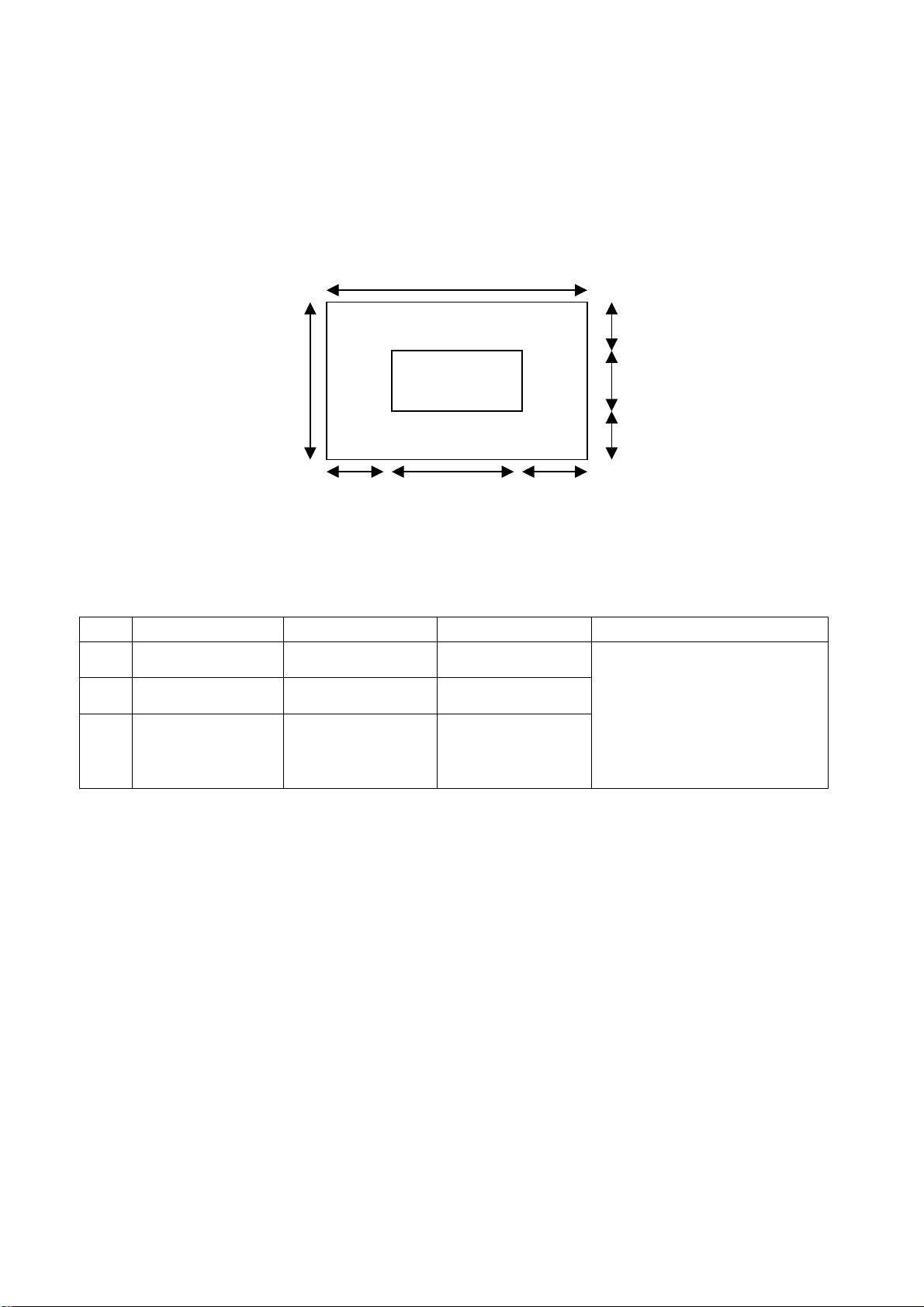
There may appear three kinds of defective points for this model as shown in Fig.1, i.e., bright spot
(remain bright); dark spot (non-illuminating); flickering spot (continuously flickering).
However they should not exceed the specification as in table 1. Otherwise the product shall be deemed
as sub-standard.
Zone B
W/4 W/2 W/4
Figure 1 Defective Points
Zone A
W
H/4
H/2
H/4
Table 1 Criterion for Three Kinds of Defective Points
Kind Area A Area B Remark
Dark spots No more than 2 No more than 8
Bright spot No more than 1 No more than 2
Total number of defective
points in A and B shall not
exceed 8. The distance
Flickering spot No more than 1 No more than 2
between two defective
points shall not be shorter
than 15mm.
2.2 Model PH-42XX:
3
Page 6
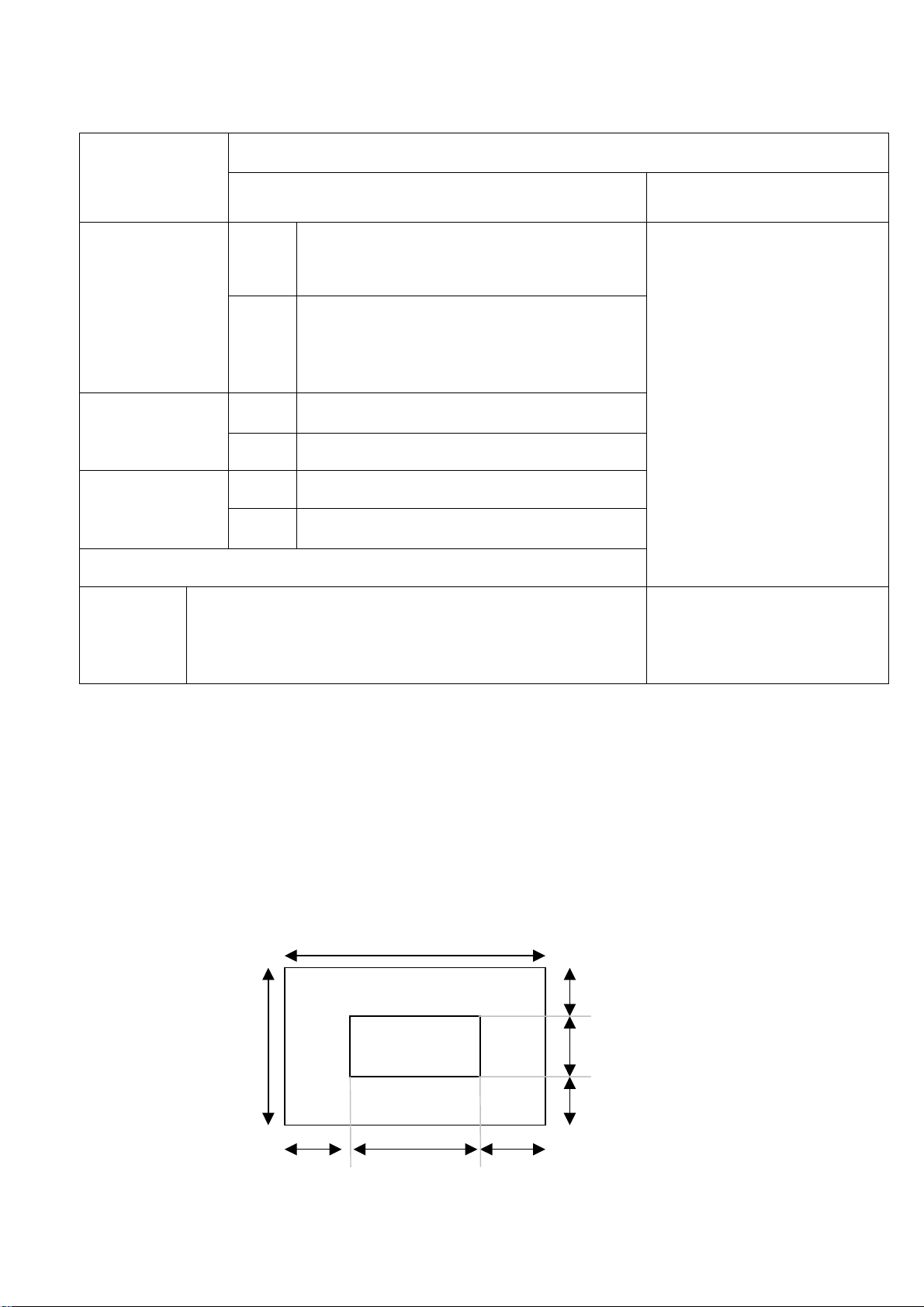
Table 2 Cell Defect Specifications
V
Defect
Number of Cell Defects (N)
►Total N≤4 [cells/full screen]
Non-Ignition
1)
Dot*
+Unstable Dot*2)
A-zone
B-zone
►N≤2 [cells/each R,G,B screen]
►N=0 [adjacency of 2-cells/full-white screen]
►Total N≤11 [cells/full screen]
►N≤5 [cells/each R,G,B screen]
►N≤5 [adjacency of 2-cells/full-white screen]
=0[adjacency of 3-cells/full-white screen]
Uncontrollable
3)
Dot*
Non-Extinguishing
4)
Dot*
A-zone ►N≤1 [cells/each R,G,B screen]
B-zone ►Total N≤3 [cells/ full screen]
A-zone ►N=0
B-zone ►N=0
►Total sum of all defects N≤17 [cells/full-white screen]
Specification
Distance between two defects
(D)
►A-Zone:≥100mm
►B-Zone: N≤2
(100mm circle/screen: 2points
allowed)
►A, B Zone overlap: N≤2
(100mm circle/screen: 2points
allowed)
►N≤6, for the stain of which longer-axis length is 5mm or
Stain*
5)
►N=0, for the stain of which longer-axis length is longer than
shorter.
►D≥50mm
5mm.
1) Non-Ignition Dot (Dark Defect) is defined as “A cell of which more than 50% area is not ignited”
2) Unstable Dot (Flickering) is defined as “A cell which repeats On and Off”
3) Uncontrollable Dot is defined as “A cell which is distinctly brighter or darker than other cells around it”
and/or “A cell of which color is distinctly different from that of other cells around it”
4) Non-Extinguishing Dot (brightness defect) is defined as “A cell of which more than 50% area is
always ON”
5) Stain is defined as “A blob due to local color contamination in white or simple color pattern”
●The decision distance is 3H away from the panel, intensity of illumination is between 100 Lux and 200
Lux.
H
V/4
A -Zone
(25% of display area)
B -Zone
(75% of display area)
V/2
V/4
H/4 H/2 H/4
4
Page 7
H
2.3 Model PH-50XX:
There may appear three kinds of defective points for this model as shown in Fig.3 i.e., bright spot
(remain bright); dark spot (non-illuminating); flickering spot (remain flickering).
However they should not exceed the specification as in table 3. Otherwise the product shall be deemed
as sub-standard.
Table 3 Criterion for Three Kinds of Defective Points
Zone B
Figure 2 Defective Points
Zone A
W
H/4
H/2
H/4
W/4 W/2W/4
Item Kind Area A Area B Remark
1 Dark spots No more than 4 No more than 10
2 Bright spot No more than 1 No more than 3
Total number of defective
points in A and B shall not
exceed 14. The distance
3 Flickering spots No more than 1 No more than 3
between two defective
points shall not be shorter
than 10mm.
5
Page 8
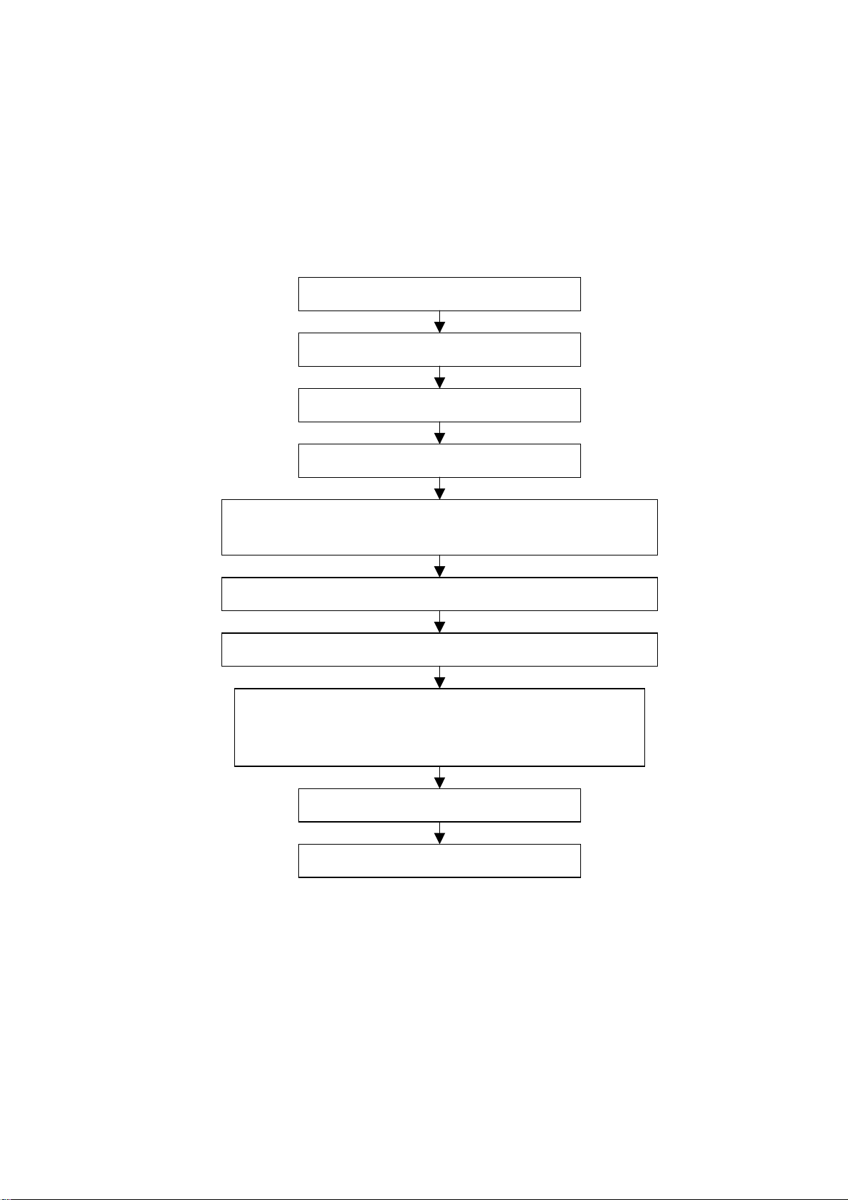
Alignment instructions
h
1. Test equipment
PM5515 (video signal generator)
VG-849 (YUV, VGA, HDMI signal generator)
CA100 (white balancer)
2. The alignment flow chart (see below figure)
Connect with central signal source, then check each function of TV such as
station missing, analog control etc., check the output of headphone and speaker
Input AV/SVIDEO signal, then check each function of all the terminals
Input HD signal (format), then check each function of the terminal
Input VGA, HDMI signal, check if the display is normal, check eac
function such as analog control etc., check horizontal /vertical center etc.
3. Description of adjustment
3.1 Unit adjustment
To produce digital board and analog board
Check the accessories and pack them in box
Check DDC and FLASH
All testing
Adjust white balance
Preset ex-factory
Fig-1 adjustment flow-chart
Connect the digital processing board, analog board, power board, power filter board and button
board according to the wiring diagram 203-PH42FB8-01JL. Connect with power and observe the
display.
Method for using factory menu: press ”INPUT” button, then press”2580” to enter level one factory
menu. Press ”CH+” and “CH-“ to select adjustment page, then press “OK” to access. Press “CH+”
6
Page 9

and “CH-“ to move cursor up and down, when the cursor stays on a certain adjustment item, press
“VOL-“ and “VOL+” to adjust. Press “MENU” exit to the level one factory menu; press “EXIT” to exit
from the factory menu at any situation.
Note: channel switch isn’t available at adjustment menu, only after return to level one factory menu,
you can switch channel.
3.2 adjustment of white balance
3.2.1 input 16 level gray-scale signal from VG849 to HDMI channel (TMIING: select a support
format of HDMI), enter white balance adjustment page of factory menu, select cool color
temperature of item, fixed WBGG_HDMI to 50H, adjust WBRG_HDMI, WBBG_HDMI, let the color
coordinate of third level on the right be (270,283) at 120nits; fixed WBBO_HDMI to 50H, adjust
WBRO_HDMI, WBGO_HDMI, let the color coordinate of third level on the left be (270,283) at 5nits.
The brightness of 120nits and 5nits may obtain by adjusting the contrast and brightness of menu.
3.2.2 input 16 level gray-scale signal from VG849 to AV channel (TMIING:968), enter white balance
adjustment page of factory menu, select cool color temperature of item, fixed WBGG_NTSC to 50H,
adjust WBRG_NTSC, WBBG_ NTSC, let the color coordinate of third level on the right be (270,283)
at 120nits; fixed WBBO_ NTSC to 50H, adjust WBRO_ NTSC, WBGO_ NTSC, let the color
coordinate of third level on the left be (270,283) at 5nits. The brightness of 120nits and 5nits may
obtain by adjusting the contrast and brightness of menu.
3.2.3 input 16 level gray-scale signal from VG849 to VGA channel (TMIING: select a support format
of VGA), enter white balance adjustment page of factory menu, select cool color temperature of
item, fixed WBGG_VGA to 128, adjust WBRG_ VGA, WBBG_VGA, let the color coordinate of third
level on the right be (270,283) at 120nits; fixed WBGO_VGA to 128, adjust WBRO_VGA,
WBBO_VGA, let the color coordinate of third level on the left be (270,283) at 5nits. The brightness
of 120nits and 5nits may obtain by adjusting the contrast and brightness of menu.
3.2.4 input 16 level gray-scale signal of 480I from VG849 to YPbPr channel, enter white balance
adjustment page of factory menu, select cool color temperature of item, fixed WBRG_YPbPr480I,
WBGG_YPbPr480I, WBBG_YPbPr480I to 128, and WBRO_YPbPr480I to 128, adjust
WBRO_YPbPr480I, WBBO_YPbPr480I, let the color coordinate of third level on the left be (270,283)
at 5nits. The brightness of 5nits may obtain by adjusting the contrast and brightness of menu.
Input format signals separately list on table 1, repeat the operation above until the white balance
pass muster.
Note: the white balance adjustment of VGA and YPBPR must be done at the situation that the white
balance adjustment of HDMI is accurate.
4 Performance check
4.1 TV function
Connect RF-TV terminal to the central signal source, enter the setup menu→ auto search, check if
there is station skipping, the output of earphone and speaker, the picture are normal.
4.2 AV/S-VIDEO terminal
Input AV/S signal, check if the picture and sound are normal.
4.3 YPbPr/YCbCr terminal
Input YUV signal (VG-849 signal generator), separate input YUV format signal of table 1 and check
if the picture and sound are normal.
Table 1 YUV signal format
No H-frequency (KHz) V-frequency (KHz) Signal
1 15.734 59.94 SDTV 480i
7
Page 10
2 31.469 59.94 HDTV 480p
3 44.955 59.94 HDTV 720p
4 33.716 59.94 HDTV 1080i
4.4 VGA terminal
Input VGA signal (VG-849 signal generator), separate input VGA format signal of table 2 and check
if the picture and sound are normal. If the image is deflection of the H-field, select manual correction
of Advanced Video Menu.
4.5 HDMI terminal
HDMI signal format receives the three high-definition signals: 480I, 480P, 720P/60Hz, 1080I/60Hz,
except for the table 2 signal. Check if the image (contain HDCP ON and OFF) and sound are
normal.
Table 2 VGA signal format
No Resolution H-frequency(kHz) V-frenquency(Hz)
1 720 X 400 31.469 70.086 28.322 IBM
2 640 X 480 31.469 59.94 25.175 IBM
3 640 X 480 37.861 72.809 31.5 VESA
4 640 X 480 37.5 75 31.5 VESA
5 640 X 480 43.269 85.008 36 VESA
6 800 X 600 35.156 56.25 36 VESA
7 800 X 600 37.879 60.317 40 VESA
8 800 X 600 48.077 72.188 50 VESA
9 800 X 600 46.875 75 49.5 VESA
10 800 X 600 53.674 85.061 56.25 VESA
11 1024 X 768 48.363 60.004 65 VESA
12 1024 X 768 56.476 70.069 75 VESA
13 1024 X 768 60.023 75.029 78.75 VESA
Point clock pulse
frenquency(MHz)
Remark
5 Ex-factory setting of user menu
1) Select TV channel, volume: 25
2) Video menu, Picture Mode: Nature, Aspect Ratio: Wide
3) Video menu, Advanced Video Menu:
Noise Reduction——Spatial: On
Noise Reduction——Speckle: Off
Noise Reduction——Temporal: On
Sharpness: 0
Tint: 50
Color Temperature: Cool
3D Y/C: On
4) Audio menu, Sound Mode: News, Balance: 31, Earphone Vo1:31
Digital Audio Output: AC-3, MTS: Mono
5) Setup menu, Tuning Band: Air
6)
8
Page 11
6) Feature menu, Sleep Timer: Off, Menu Language: English
Note: Except for Color Temperature of Cool, the Advanced Video Menu of YPbPr/YCbCr and VGA
channels sets according to the adjustment of factory.
Trouble shooting
Before servicing please check to find the possible causes of the troubles according to the table
below.
1.Antenna(signal):
Picture is out of focus or jumping Bad status in signal receiving
Poor signal
Check if there are failures with the electrical connector or
the antenna.
Check if the antenna is properly connected.
Fringe in picture Check if the antenna is correctly oriented.
Maybe there is electric wave reflected from hilltop or
building.
Picture is interfered by stripe
shaped bright spots
There appear streaks or light color
on the screen
2.TV set:
Symptoms Possible cause
Unable to switch the power on Check to see if the power plug has been inserted
No picture and sound Check to see if the power supply of liquid crystal TV has
Deterioration of color phase or
color tone
Screen position or size is not
proper
Possibly due to interference from automobile, train, high
voltage transmission line, neon lamp etc.
Maybe there is interference between antenna and power
supply line. Please try to separate them in a longer
distance.
Maybe the shielded-layer of signal wire is not connected
properly to the connector.
Check if interfered by other equipment and if interfered
possibly by the equipment like transmitting antenna, non
professional radio station and cellular phone.
properly into the socket.
been switched on. ( as can be indicated by the red LED
at the front of the TV set)
See if it’s receiving the signal that is transmitted from
other source than the station
Check if it’s connected to the wrong terminal or if the
input mode is correct.
Check if the signal cable connection between video
frequency source and the liquid crystal TV set is correct.
Check if all the picture setups have been corrected.
Check is the screen position and size is correctly set up.
9
Page 12
Symptoms Possible cause
Picture is twisted and deformed Check to see if the picture-frame ratio is properly set up.
Picture color changed or colorless Check the “Component” or “RGB” settings of the liquid
crystal TV set and make proper adjustment according to
the signal types.
Picture too bright and there is
distortion in the brightest area
Picture is whitish or too bright in
the darkest area of the picture
No picture or signal produced from
the displayer if “XXX in search”
appears.
There appears an indication “outside the receivable scope)
Remote control cannot work
properly
No picture and sound, but only
hash.
Blur picture Check if the antenna cable is correctly connected.
No sound Check if the “mute” audio frequency setting is selected.
When playing VHS picture search
tape, there are lines at the top or
bottom of the picture.
Check if the contrast setting is too high.
Possibly the output quality of DVD broadcaster is set too
high.
It maybe also due to improper terminal connection of the
video frequency signal in a certain position of the
system.
Check if the setting for the brightness is too high
Possibly the brightness grade of DVD player
(broadcaster) is set too high.
Check if the cable is disconnected.
Check if it’s connected to the proper terminal or if the
input mode is correct.
Check if the TV set can receive input signal. The signal is
not correctly identified and VGA format is beyond the
specified scope.
Check if the batteries are installed in the reverse order.
Check if the battery is effective.
Check the distance or angle from the monitor.
Check if there is any obstruct between the remote control
and the TV set.
Check if the remote control signal- receiving window is
exposed to strong fluorescence.
Check if the antenna cable is correctly connected, or if it
has received the video signal correctly.
Of if it has received the right video signal.
Check if the sound volume is set to minimum.
Make sure the earphone is not connected.
Check if the cable connection is loose.
When being played or in pause VHS picture search tape
sometimes can’t provide stable picture, which may lead
to incorrect display of the liquid crystal TV, In this case
please press “auto” key on the remote control so as to
enable the liquid crystal TV set to recheck the signal and
then to display correct picture signal
10
Page 13
Method of software upgrading
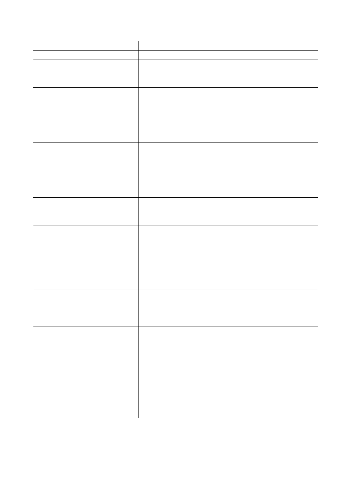
1. Connect RS-232 cable to computer and TV set. The cable must be a female to female RS-232
cable, and the line is TXD to RXD and RXD to TXD cross-link. It’s popular for PC to PC
connection.
2. If the computer has no RS-232 serial port(e.g. Notebook PC),you needs a additional USB to serial
port cable.
11
Page 14
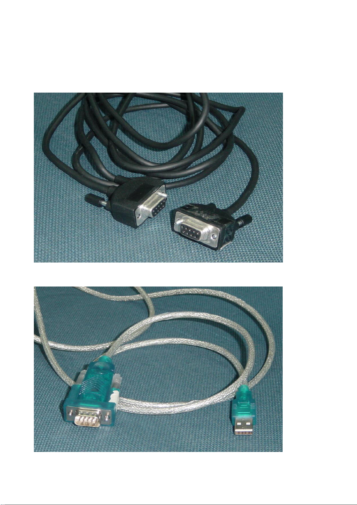
3. Copy the update tools (iDev.exe) to the path you want to do it, and double click it.
4. Select “setup” menu.
5. Confirm the Serial port is right. Base on the port which using for update. And set the band rate to
115200 (default).
12
Page 15
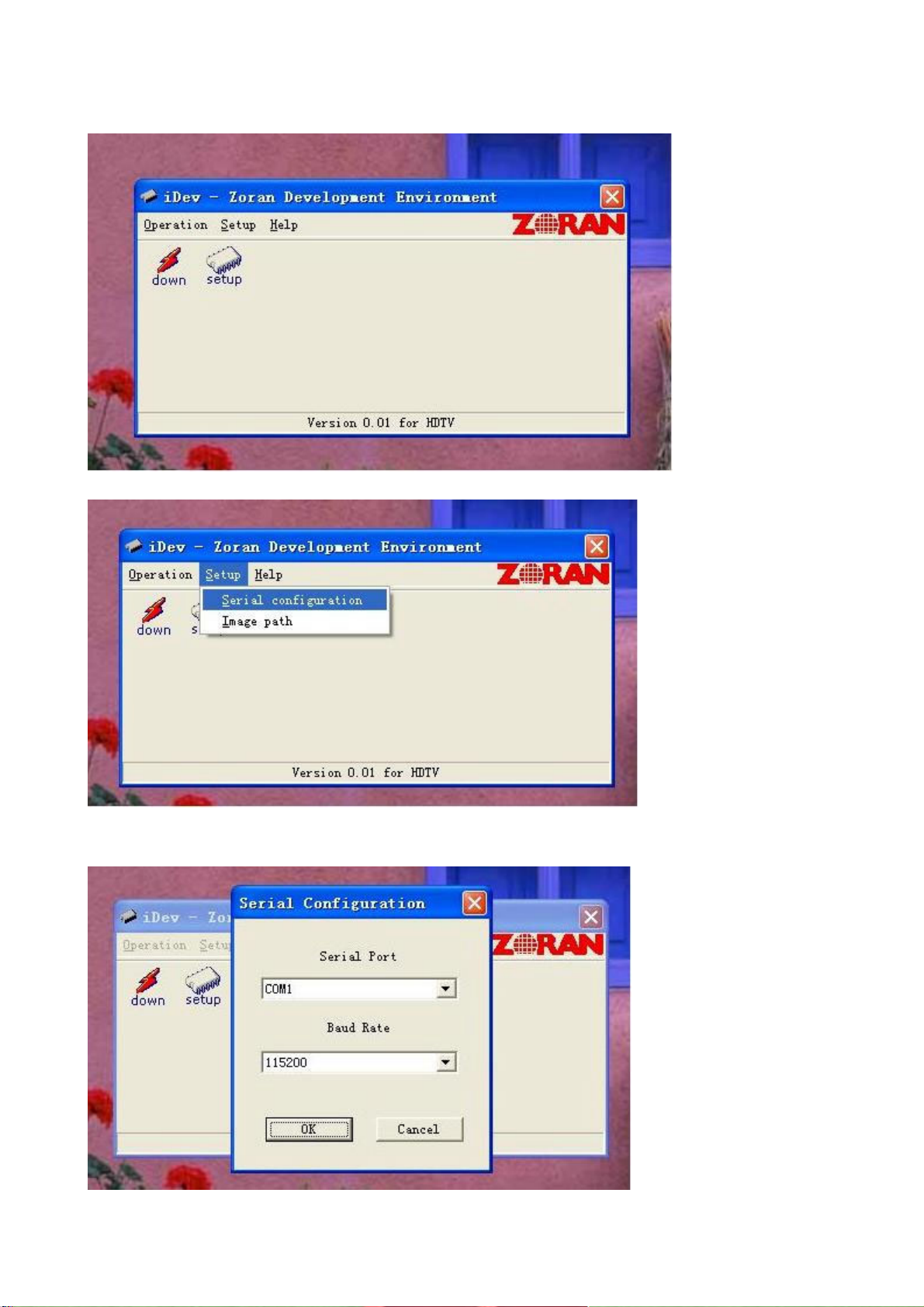
6. Select the “Image path” menu.
7. Confirm it’s the right file.
8. If it’s not right(Maybe you didn’t select it before),click the “…”button to select “*.ecc” file. Sometimes
the image file you got it will be “*.rar ”or “*.zip” zip file, needs unzip it first.
13
Page 16
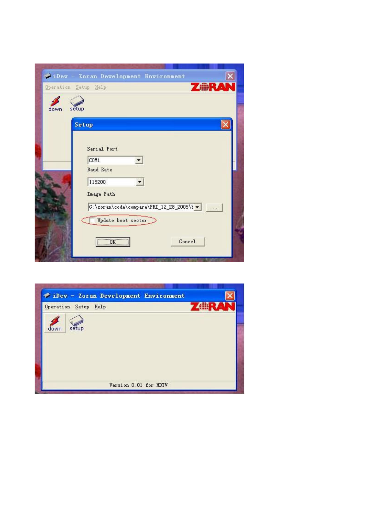
9. You also can click the setup button to select and config, but please don’t select the red
one(update boot sector).
10. Then click the “down” button.
14
Page 17
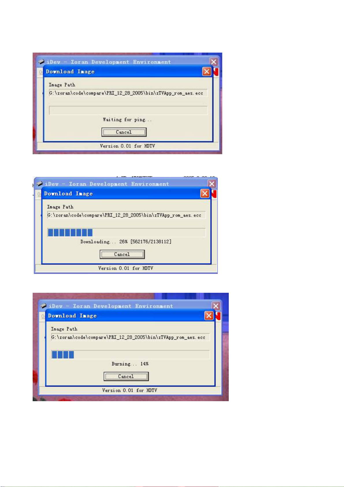
11. You can see the “waiting” window.
12. Then power (off then) on the TV set.
13. After download, it will be burning.
15
Page 18
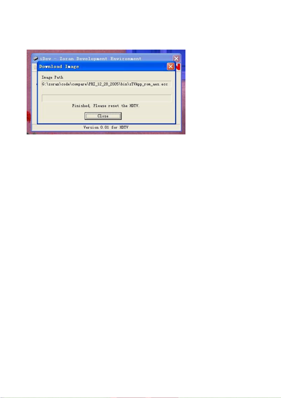
14. Last it will be finished
15. Press the (IR/ locate keypad) power key and holding for several second to force power off TV set,
then power on again. It would be ok now. If it’s failure you can try once again.
16
Page 19

Working principle analysis of the unit
1. NTSC signal flow:
Antenna reception NTSC signal send to the integrative tuner FQD1236, which contains HF and IF
amplifier circuit and video decoding circuit. It is controlled by main IC ZR39660 (inside CPU)
through I2C bus. The NTSC signal via frequency tuning, HF amplification, IF amplification, system
switching and decoding, output video signal TV-CVBS of 1Vpp and sound IF signal (SIF).
TV-CVBS and AV1-CVBS, AV2-CVBS input from AV terminal, via switch IC HEF4052 to output
signal, one way send to ZR39660 for VEDIO DECODER, DEINTERLACE and SCALER, then send
to LVDS level drive for LCD screen, another way is output through AV output socket as AV OUT.
The sound IF (SIF) is fed into demodulation IC CAS220, via decoding and A/D conversion, it is fed
into ZR39660 for analog control in the format of I2S. ZR39660 outputs audio data of I2S format, it is
fed into audio D/A converter IC CS4344, output analog L/R signal. The L/R signal and sound signal
of PC/YPRPB via diverter switch HEF4052BT, send to R2S15900SP (sound processing and volume
control). Select right/left sound channel, their send to digital sound amplifier TPA3001 amplify, then
send to speaker.
2. ATSC signal flow:
Antenna reception ATSC signal send to tuner FQD1236, after frequency tuning, HF amplification, IF
amplification and SAW FILTER, output IF signal to demodulation chip CAS220, via VSB or QAM
demodulation, Sound stereo decoder, fed to ZR39660 for information source decoding in the format
of standard serial TS stream.
HD video signal via decoding to A/D conversion and OSD superposition, at last send to LVDS drive
level for PDP panel.
HD audio signal, via decoder built-in ZR39660, resumed to multi- channel sound of Dolby AC-3, at
the same time output data stream of I2S format and S/PDIF data stream. Audio data of I2S format is
fed to audio D/A conversion chip CS4344 to output analog L/R signal. S/PDIF data stream directly
output from optical fiber interface.
3. PC/YPrPb signal flow
PC and two YPBPR signal via matched resistance, it a-c couple to video switch SN74CBT3257CDR,
via switching to selected signal to Triple Video A/D Converter MST9883 A/D conversion. Send
B/G/B of 24 bit to main IC ZR39660 digital decode, image scale and OSD superposition, then send
to LVDS level drive for LCD screen.
Sound signal (PC, YPrPb) via switch diverter HEF4052BT to output signal, it send to R2S15900SP
(sound processing and volume control) switch of audio. Select right/left sound channel, their send to
digital sound amplifier TPA3001 amplify, then send to speaker.
4. HDMI signal flow
HDMI video signal is directly fed to main IC ZR39660 (with HDCP function of HDMI) digital decode,
image scale and OSD superposition, then output LVDS drive level for screen.
HDMI audio signal, via decoder built-in ZR39660,output data stream of I2S format and S/PDIF data
stream at the same time. Audio data of I2S format is fed to audio D/A conversion chip CS4344 to
output analog L/R signal. S/PDIF data stream directly output from optical fiber interface.
17
Page 20
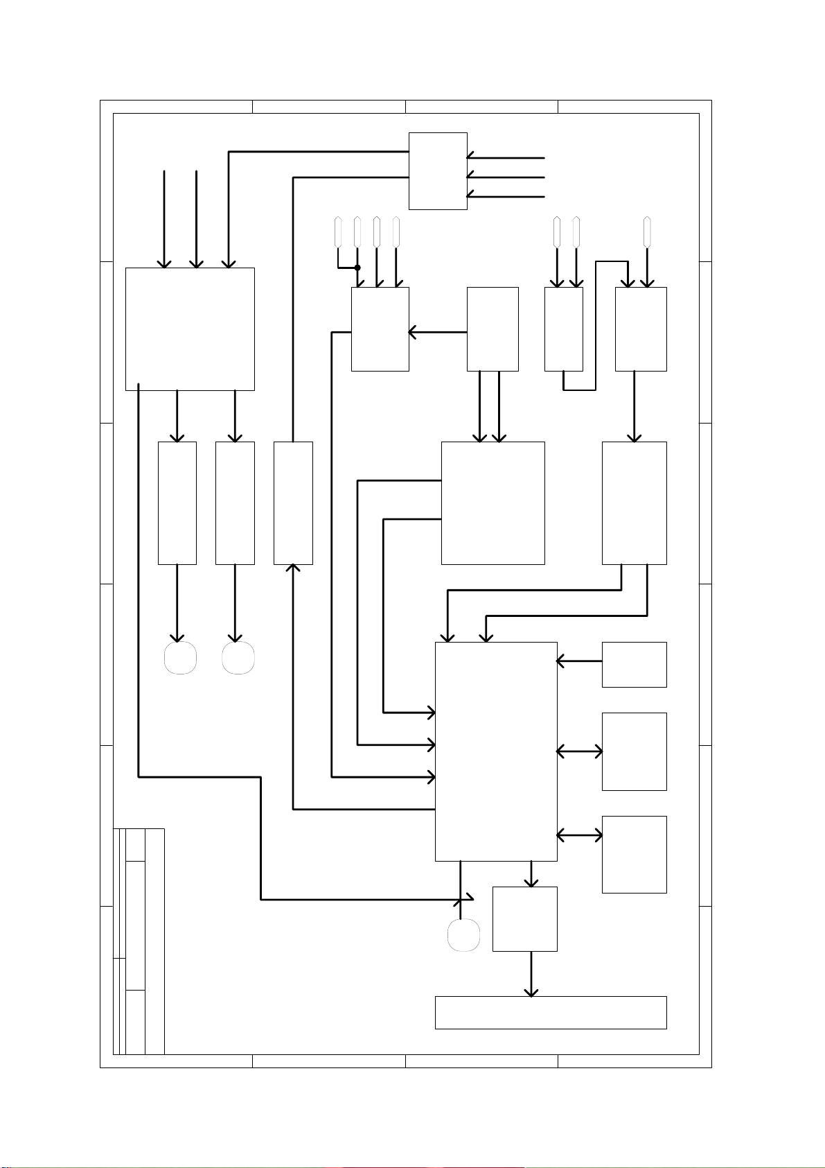
Block diagram
A
AV1 AUDIO
1 2 3 4 56
AV2 AUDIO
B
CVBS2
CVBS1
S_Y
S_C
R2S15900SP
HEF4052BT
CVBS_TV
NJW1109
TPA3001D1
D/A CS4344
SN3253C
C
YPBPR1 AUDIO
YPBPR2 AUDIO
PC AUDIO
FQD1236 MK5
TUNER
Analog SIF
Digital IF
CAS220CS
YPBPR1
SN3257C
D
YPBPR2
PC
SN3257C
RGB/YUV
MST9883
Earphone
Loudspeaker
ZORAN PS-42J6
HS,VS,CLK
IIS IN
IIS OUT
TS
CVBS,Y/C
24-BIT Data
HDMI
ZR39660
BGA400
AV_OUT
JEPICO
j-L003
LVDS
M29W320E
FLASH
2X16MX16
DDRAM
54321
V1.0
6
Panel
A
B
C
D
18
Page 21

IC block diagram
1. ZR39140
19
Page 22

Pin descriptions of ZR39660:
(1) Serial Transport Input Port
T4: MPEG Transport Port Input Clock
T3: MPEG Transport Input Data
U3: MPEG Transport Input Frame
Y1: MPEG Transport Input Valid
(2) HDMI Input
D1,E3,F3,E2,F2,E1: HDMI Differential Data Pairs
D2,C1: HDMI Differential Clock Pair
C3: HDMI Serial Clock
B2: HDMI Serial Data
A1: HDMI Hot Plug Detect
D3: HDMI Current Set
(3) NTSC/PAL Analog Input Port
W2: Video Front End Luminance In
Y3: Video Front End Chroma In
W3: Video Front End Common Mode Reference
(4) Analog Video Output
K18: Composite Data Output (CVBS)
J20: Blue/Pb Pixel Data Output
J18: Green/Y Pixel Data Output
J19: Red/Pr Pixel Data Output
(5) Audio I/O
R2: Audio Clock
R3: Bit Clock
P3: Left/Right Channel Selector
U2: Serial Audio Data Input
T2: Serial Audio Data Output
V1: IEC958 Format Out
(6) LVDS Panel Interface
B20,C19: Output Clock Pair
E18,F17: Output Data Pairs 0
C20,D19: Output Data Pairs 1
F18,G17: Output Data Pairs 2
D20,E19: Output Data Pairs 3
E20,F19: Output Data Pairs 4
H18,G18: Output Data Pairs 5
F20,G19: Output Data Pairs 6
G20,H19: Output Data Pairs 7
D18 : External Resistor Connection
20
Page 23

(7) UART and I2C Interface
N1: UART 0 Transmit
P1: UART 0 Receive
R1:I2C Compatible Clock 0
P2:I2C Compatible Data 0
M3:I2C Compatible Clock 1
M2:I2C Compatible Data 1
(8) Miscellaneous
M4, N3: Two pins required to support the 24.576 MHz crystal
N5: Power On Reset
L4: Infrared Receive
2. j-L003(Higobashi)
The j-L003(Higobashi) LSI provides a variety of image quality adjustment functions designed to
produce sharp, well-defined coloration in personal computer LCD monitors and LCDTV screens, as
well as dot-matrix displays in rear projection TVs, PDPs, and other devices.
The image-enhancement functions built into the j-L003 use a proprietary color management
technology that makes it possible to produce images that are closer than ever to nature. The j-L003
also includes black-white stretch, brightness correction, horizontal edge enhancement, and gamma
correction functions: these expand your capabilities even farther, to enable you to achieve your own
custom image-processing methods.
21
Page 24

Pin configuration of j-L003:
(1) TTL SIGNAL INPUT
71: VS INPUT 72: HS INPUT 73: DE 76: CLK INPUT;
74, 78, 79, 80, 81, 82, 84, 93: RED Signal INPUT;
94, 95, 96, 97, 98, 99, 101, 102: GREEN Signal INPUT;
103, 104, 106, 107, 108, 109, 110, 111: BLUE Signal INPUT;
(2) TTL SIGNAL OUTPUT
65: VS OUTPUT 66: HS OUTPUT 67: DE 34: CLK OUTPUT
05, 06, 07, 08, 09, 10, 11, 13: RED Signal OUTPUT
14, 15, 16, 18, 19, 20, 21, 22: GREEN Signal OUTPUT
23, 24, 26, 27, 28, 29, 30, 31: BLUE Signal OUTPUT
(3) I/O CONTROL
148: RESET 151: SMMRSE 156: ADID0 157: ADID1
3. CAS220/CS
The CAS-220/CSO is a multi-standard demodulator and decoder for terrestrial and digital cable TV
reception. It is designed to support 8-VSB (Vestigial Side Band) in full compliance with ATSC Digital
Television Standards, ITU-T J.83 Annex B, and OpenCable™ Out-of-Band Signaling. The
CAS-220/CSO also demodulates analog BTSC and Korea A2 sound.
Its basic function is to recover the digital data encoded into the broadcast signal, which includes
video and sound program information and ancillary data service.
22
Page 25

Pin configuration of CAS220/CS:
Pin descriptions of CAS220/CS:
61: RESET_N
79, 80 oscillator
13 Select I2C address
16: I2C data for host communication with the tuner
18: I2C clock to the tuner
19: I2C clock from host
20: I2C data from/to host
93,94: Differential input for IF
96,97: Differential input for SIF
63: Digital Sound Word select (L/R select)
65: Digital Sound Serial data output
66: Digital Sound Serial clock.
17,30,46,62,74,82,84: Power Supply 3.3V
5,9,22,37,53,69,75,78,86,87,99: Power Supply 1.8V
6,7,15,23,33,35,45,55,60,70,73,76,77,81,83,85,88,91,92,95,98: Ground
23
Page 26

4. MST9883
MST9883 is a Triple Video A/D Converter with Clamps & Pixel Clock Synthesizer. The triple ADC
support 12 - 110 MHz Sampling Rate. It integrated 5-bit pixel clock phase adjustment for precise
sample timing control. It’s Output support 4:2:2 Format Mode and it can Pin Compatible with
AD9883A.
Block diagram of MST9883 is flow:
24
Page 27

Pin configuration of MST9883:
Pin descriptions of MST9883:
54: Red analog input
48: Green analog input
43: Blue analog input
49: Sync on Green analog input
38: External Clamp Input
30: Horizontal SYNC Input
31: Vertical SYNC Input
29: Hold PLL Frequency, do not track HSYNC
56: Serial Interface clock
57: Serial Interface data pin
55: Serial interface address pin
70-77: Red output data
2-9: Green output data
12-19: Blue output data
67: Output data clock
66: HSYNC output
64: VSYNC output
39,42,45,46,51,52,59,62: Analog Power
25
Page 28

26,27,34,35: PLL Power
11,22, 23, 69,78,79: Digital Output Power
1,10,20,21,24,25,28,32,36,40,41,44,47,50,53,60,61,63,68,80:Ground
5. R2S15900SP
R2S15900SP is an audio signal processor. It has MUTE and Volume/Tone control. It can support 5
input selector.
Pin descriptions of R2S15900SP:
2,27: AV1 AUDIO INPUT L/R
3,26: AV2 AUDIO INPUT L/R
4,25: DTV AUDIO INPUT L/R
5,24: EAR PHONE L/R
6,23: AV OUT L/R
11,19: AUDIO OUTPUT L/R
17,18:I2C SDA/SCL
28: Power Supply
12: Ground
26
Page 29

6. TPA3001
The sound power amplifier TPA3001 Class D AMP is the high effective D type of power amplifier of
the single track. The output power can reach 20W with 8-Ω speakers, +18V power supply,
eliminating the need for heat sinks. The TPA3001D1 is available in the 24-pin thermally enhanced
TSSOP package.
Pin configuration of TPA3001:
Pin description of TPA3001:
1: Negative differential input
2: Positive differential input
3,4: gain control
10,11: Negative BTL output
14,15: Positive BTL output
9,16,24: Power Supply
6,12,13,18,19: Power Ground
5: Shutdown terminal
27
Page 30

Wiring diagram
Butt on bo ard
(667 -PH42F B6 -05)
RS-232 HDMI VGA
S/PDI F
Digital processing board
YpbPr 1 YpbPr 2
5 6 5 5 9
XC01XB01XC02
XB03 X801 X603
`
Logical board
LA03
XA50
31 6 12 11 4 6
667 -PS42FB6 -69
X802
X602
Powe r boa rd
X603
Panel
335
42012
00
(667
PS42D8
X608
X601
-
20)
X606
X501
5
X232X103X102
X231 X101 X226
AV out Earph one S-Video AV1 in AV2 in
X105
2
Analog board
667-PS42FB6-53
X106
Speaker assy
Power filter board
X104
4
RF
28
Page 31

Diagnosis for Plasma Screen of PH42/50FBXX
)
And Maintenance of the Functions of Various Modules on Screen
1. Functions of Various Modules on Screen
As shown in the figure below, PDP screen can be divided into power supply board, X driving board, Y
driving board, logic board, logic BUFFER board (E, F, G), Y BUFFER board (upper and lower), COF etc.:
Y BUFFER(up)
Y driver board
Y BUFFER(down)
Logic
BUFFER(E)
Logic
BUFFER(F
Power supply board
Logic board
X driver board
Logic
BUFFER(G)
* Power supply board: to supply power for the screen, other functional modules on the screen, our own
main board, and video frequency processing board.
* X driving board: to produce and provide driving signal for X electrode according to the time sequence
signal sent from logic board.
* Y driving board: to produce and provide driving signal for Y electrode according to the time sequence
signal sent from logic board.
*Logic board: to process the image signal sent from the main board, to produce addressing signal and
to provide driving signal for X and Y driving boards.
*Logic BUFFER board (E, F): To convert the data signal and control signal sent from the logic board
into the signals required by COF
*Y BUFFER board(Upper,Lower): to transmit the scanning signal from the Y driving board to the
screen, which is divided into upper and lower parts.
*COF: to convert the signal sent from the logic BUFFER board into the address signal used by the
screen.
COF(7 blocks)
29
Page 32

2. Trouble diagnosis:
1) The screen is not bright:
a. Check to see if the power supply plug from the power filter board to the power supply board is
well inserted into the socket. If not, plug it in.
b. Check if the fuse on the power supply board is blown up. If yes, replace it for a good one.
c. Remove digital processing board and analog board, ground socket X601 of the power supply
board to the AUTO mode.
Switch the power on and check if the output voltages of the power board are normal. If
normal, then the problem lies in digital processing board and analog board, which will be
dealt with separately. If abnormal, then first replace the power supply board to see if the
problem is solved.
2) There appears on the screen a line or several unlit lines.
Check if the socket between Y driving board and Y BUFFER is plugged well. If not, plug it well. If
yes then replace Y BUFFER (upper, lower) in respect to the upper , lower part of the dark line on
the screen.
3) There appear on the screen one or several horizontal lines that are much brighter than the
remaining horizontal lines at the edge:
Check if the socket between Y driving board and Y BUFFER is plugged well. If not, plug it well. If
yes then replace Y BUFFER (upper, lower) in respect to the upper , lower part of the dark line on
the screen.
4) There appear on the screen one vertical unlit line or a vertical entirely unlit block
30
Page 33

a. If it’s one vertical unlit line, then COF has problem.
b. If it’s a vertical entirely unlit block, then first check if the connection socket between COF and
logic BUFFER has problem. If not, check if the connection socket between the logic BUFFER
and the logic board is normal. If yes, replace the logic BUFFER. Finally, if the problem still
remains when the replacement is over, then replace the logic board.
5) There appears on the screen a mono color signal and one or several vertical bright lines of other
colors:
a. If it’s a vertical bright line of other colors, then the problem lies with COF or the screen.
b. If it’s an entire vertical block of other colors, then first check to see if the connection socket
between COF and logice BUFFER has problem. If no problem, check if the connection
socket between the logic BUFFER and the logic board is normal. If it’s normal, then
replace the logic BUFFER. If the problem still remains after the replacement, then replace
the logic board. Finally if the problem is still there, then the problem lies with COF.
6) There appear on the screen abnormal bright spots or blocks that are different from what’s
described above:
a. Check if the connection socket between COF and logic BUFFER board has been well
plugged.
b. Replace the logic BUFFER board. If it’s not solved then replace logic board. If the problem
still remains, then it’s the problem with COF.
31
Page 34

Troubleshooting guide
r
N
N
N
d
N
p
N
p
Yes, turn the unit on
If the picture of each channel
is normal?
If the sound of each channel is
normal?
(1) abnormal picture
a) Failure with resistor rows R839~R844 of image processing board, which may lead to lack of
b) Failure with resistor rows R825~R830 of image processing board, which may lead to lack of
c) A certain differential wire pair of LVDS of XA50 or X803(RX0+/-, RX1+/-, RX2+/-, RX3+/-)is
d) Failure with resistor rows RA18~RA25, which may lead to loss of corresponding color from
e) Failure with NB07,NA51 and their peripheral circuit, which may lead to picture abnormal of
f) Failure with N104, which may lead to picture abnormal of TV, AV1, AV2, S-VIDEO.
g) Failure with N803/N805/N806, which may lead to picture abnormal in all channels.
Begin
A red indicator
lights?
A blue indicator
lights?
Ye s
Display picture?
Ye s
color or color splash.
color or color splash.
abnormal, which may lead to lack of color or color splash.,
the gray degree corresponding to the picture of channel HDMI.
PC, YPrPb and YCrCb.
o
o
o
o
o
Check power board , button board and powe
cord
Check if the pin1 of X602 in data processing
board is high level(+5V)? check V660/V661.
Check if the crystal in data processing boar
starts, DDR clock is correct?
Check the signal inputted from the channel to
in IC or IC and its peripheral circuit or the
output of LVDS is normal
Check the signal inputted from the channel to
in IC is normal or IC(R2S15900/TPA3001)
and its periphery is normal
32
Page 35

N
r
r
b
N
N
p
p
N
r
N
f
N
d
N
(2) no picture, no sound
Red
Check the color of indicato
light
Check the powe
oard
o sound
Refer to (3) checking
rocedure
(3) with picture but no sound
With picture but no sound
Check if the voltage of sound amplifie
of X106 in analog board is normal?
Check if the pin2 o
112/N113 inputs signals
Ye s
Check N112/N113 and
their peripheral circuit
o picture, no sound
Ye s
o picture
Refer to (4) checking
rocedure
Ye s
Blue
Check the output voltage of
sockets X601~X603/X606/X608
o
Power board problem
o
Check the power board
o
Check N103/NB05 an
their peripheral circuit
33
Page 36

N
N
N
d
p
R
t
N
(4) with sound but no picture
Ye s
If there is no picture
in all channels?
Ye s
Check N108 an
its peripheral circuit
With sound but no picture
Display OSD MENU?
Ye s
Display LOGO? If pin5 of X602 (IRR) has signal?
o
Check if the crystal in data processing board starts,
DDR clock and DDR SDRAM are normal?
o
Refer to (6), (7), (8), (9), (10),
(11), (12) checking procedure
Refer to (5) checking
rocedure
o
Ye s
o
Check N801, N802, DD
and their peripheral circui
and power supply
34
Page 37

(5) Check image processing board
y
N
N
f
N
N
r
N
d
p
d
p
Check the power suppl
of N803
Ye s
o
Check if pin20, 21, 27,
30 of X801is high level
Check if the power supply of
L801/L802 are normal
Ye s
o
Check if pin3, 5, 26 of N806
output H/V-SYNC and clock
Check the peripheral and power supply o
801, N802, DDR of data board
o
Ye s
Check the peripheral and powe
supply of N806
Check if pin34, 65, 66 of N803 output
H/V-SYNC and clock
o
Ye s
Check the peripheral an
ower supply of N803
Check the peripheral an
ower supply of N805
Note: please make sure that the data of FLASH N804 is correct before checking the image
processing board.
35
Page 38

(6) AV no picture
N
N
t
p
N
N
f
N
t
t
p
Check if pin13 of N104
outputs signals?
Ye s
Check the periphery circui
from XC02 to N801
(7) S-terminal no picture
Check if pin13/3 o
104 outputs signals?
Ye s
Check the periphery circui
from XC02 to N801
Check if C136 and C137
input signals?
Ye s
o
Check if C105 and C138
input signals?
Ye s
o
o
Check N105/N106 and the circuit
from AV terminal to N104
Check N104 and its
eriphery circuit
o
Check N108 and the circui
from S-terminal to N104
Check N104 and its
eriphery circuit
36
Page 39

(8) NTSC channel no picture
N
N
t
p
N
N
f
N
f
d
p
Check if pin11 of TUNER226
output signals?
Ye s
o
Check if pin13 of N104
outputs signals?
Check TUNER226 power supply
and the peripheral circuit.
Ye s
o
Check the periphery circui
from XC02 to N801
Check N104 and its
eriphery circuit
(9) ATSC channel no picture
Check if pin6/7 of TUNER226
output signals?
Ye s
o
Check if the crystal o
228 (20MHz) is normal?
Check TUNER226 power supply
and the peripheral circuit.
Ye s
o
Check the clock signal o
each pin of XC01
Check G226, N228 an
eriphery circuit
Note :
The I2C bus line control of TUNER is switch through the bus line of N228, so after checking the power
supply and peripheral circuit of TUNER226, it is still no picture in NTSC and ATSC channel, please
check N228 emphatically.
37
Page 40

(10) YprPb or Ycrcb channel no picture
N
f
N
N
N
m
N
f
N
N
m
Check if pin4/7/9 of NB07
output signals?
Ye s
Check if pin64/66/67 o
A51 are normal?
Ye s
o Ye s
Check resistor
rows RA63~
RA68
Check NA51
and peripheral
circuit.
(11) D-sub channel no picture
Check if pin4/7/9 of NB07
output signals?
Ye s
Check if pin64/66/67 o
A51 are normal?
Ye s
o
Check resistor
rows RA63~
RA68
Check NA51
and peripheral
circuit.
o
Check if pin4/7/9 of NB08 output
signals?
Check NB01/NB02
and the circuit fro
X807/X808 to N808
o
Check NB03/NB04
and the circuit fro
X807/X808 to N808
Check NB07
and peripheral
circuit.
o
38
Page 41

p
N
f
p
p
(12) HDMI channel no picture
Check DETECT NA04 and its
eripheral circuit?
Ye s
o
Check if signals o
RA18~RA25 are normal?
Ye s
Check N801 and its
eripheral circuit
Check the connection to HDMI
socket, NA04 and its
eripheral circuit
Note: N801 embeds FLASH, which stores DDC and HDCP information of HDMI, so make sure the
connection between HDMI socket/interface and the bus line is well- going, the picture will display.
39
Page 42

Block diagram of LG 42” power board
IIC
IR
KEY
VGA_H∕V
LED
RESET
5VCTRL Va.Vs.
Overvoltage undervoltgae test.
ATMEGA8L
Input AC voltage test
MCU
Output voltage control ON/OFF
Va,Vs active dischage control
PFC OUT 400V
AC IN
EMI
Rectify
PFC
STR
–E1565
DC/DC
Isol ation
18V
STR X6769–
DC/DC
Isolation
DC/DC
STR F6468–
Isolation
Vs
Va
STR A6159M
DC/DC
–
Isolation
AP1501
Fliter
DC/DC
AP1501A
DC/DC
AP1501
DC/DC
AP1501
DC/DC
5VSB
18VSC
12VSC
5VCTRL
5VSC
3V3SC
40
Page 43

Block diagram of LG 50” power board
IIC
IR
KEY
VGA_H∕V
LED
RESET
5VCTRL.Va.Vs
Overvoltage.un derv oltg ae test
ATMEGA8L
Input AC voltage test
MCU
Output voltage control ON/OFF
Va,Vs active dischage control
PFC OUT 400V
AC IN
EMI
Rectify
L4981BD
PFC
DC/DC
STR–F6467
Isolation
18V
STR–X6769
DC/DC
Isolation
DC/DC
STR–F6468
Isolation
Vs
Va
STR
DC/DC
–A6159M
Isolation
AP1501
Fliter
DC/DC
AP1501A
DC/DC
AP1501
DC/DC
AP1501
DC/DC
5VSB
18VSC
12VSC
5VCTRL
5VSC
3V3SC
41
Page 44

Troubleshooting of LG 42” power board
Instruction of system and time sequence control
The whole system is composed of EMI, rectify, PFC, DC/DC and MCU. Therein MCU is the control
core of the whole system. On the one hand, it controls ON/OFF time sequence of each voltage and
the main, AC voltage test. On the other hand, it performs the standby CPU function with IIC bus to
the main CPU.
Time sequence
The system has two working modes: AUTO and NORMAL, AUTO mode is used for adjustment and
service, while NORMAL mode is used for TV at normal time. At AUTO mode(short X610), connect
5VCTRL with load of about 2A, turn on power, then output several low-voltage power supplies,
delay 1.5s or so and output Va, Vs. First stop the output of Va, Vs at power-down, and active
discharge to output-capacitor of Va,Vs. on condition that the voltage Va,Vs each is lower than 10
percent (if unsatisfied, then wait), then delay 0.5s and stop all the low-voltage power supplies
except for 5VSB into Standby mode.
At NORMAL mode, MCU receives power-on control of IR or button board, outputs several
low-voltage power supplies, after main CPU sending Va,Vs start-control through IIC bus, outputs
Va,Vs. at the status of turn on, MCU receives power-down control from main CPU and performs
power-down time sequence (power-down time sequence is the same at AUTO mode).
At the two modes, when detect the lower input AC voltage, it will not perform power-on. At the status
of turn on, when detect the lower input AC voltage or 5VCTRL,Va,Vs beyond normal scope value, it
will perform the power-down time sequence above and enter into Standby mode.
Trouble diagnosis
The voltage 5VSB is normal, while the voltages of other circuits are zero, in this case, it may switch
power on at AUTO mode and check if 5VCTRL delay 1.5s or so, if NO, check 5VCTRL and its
fore-circuit; if YES, check LED (LED601), if LED lights, check the circuit of Va, jf not, check the
circuit of Vs (note: premise N608 and its periphery circuit are normal). If the voltages of other circuits
are abnormal, check the corresponding circuits.
Trouble phenomenon (premise the voltage 5VSB is normal)
The main voltage of power board is abnormal, which is commonly detected to enter into Standby
mode, the phenomenon is that switch power off immediately after switching power on.
AC detect circuit or IR, button circuit is abnormal, which will lead to unable to switch power on.
The low-voltage power supplies are normal, while the voltage Va, Vs is zero, it maybe
communication abnormal of IIC bus between MCU and main CPU.
42
Page 45

Troubleshooting of LG 50” power board
Instruction of system and time sequence control
The whole system is composed of EMI, rectify, PFC, DC/DC and MCU. Therein MCU is the control
core of the whole system. On the one hand, it controls ON/OFF time sequence of each voltage and
the main, AC voltage test. On the other hand, it performs the standby CPU function with IIC bus to
the main CPU.
Time sequence
The system has two working modes: AUTO and NORMAL, AUTO mode is used for adjustment and
service, while NORMAL mode is used for TV at normal time. At AUTO mode(short X5201), connect
5VCTRL with load of about 2A, turn on power, then output several low-voltage power supplies,
delay 1.5s or so and output Va, Vs. First stop the output of Va, Vs at power-down, and active
discharge to output-capacitor of Va,Vs. on condition that the voltage Va,Vs each is lower than 10
percent (if unsatisfied, then wait), then delay 0.5s and stop all the low-voltage power supplies
except for 5VSB into Standby mode.
At NORMAL mode, MCU receives power-on control of IR or button board, outputs several
low-voltage power supplies, after main CPU sending Va,Vs start-control through IIC bus, outputs
Va,Vs. at the status of turn on, MCU receives power-down control from main CPU and performs
power-down time sequence (power-down time sequence is the same at AUTO mode).
At the two modes, when detect the lower input AC voltage, it will not perform power-on. At the status
of turn on, when detect the lower input AC voltage or 5VCTRL,Va,Vs beyond normal scope value, it
will perform the power-down time sequence above and enter into Standby mode.
Trouble diagnosis
The voltage 5VSB is normal, while the voltages of other circuits are zero, in this case, it may switch
power on at AUTO mode and check if 5VCTRL delay 1.5s or so, if NO, check 5VCTRL and its
fore-circuit; if YES, check LED (LED5201), if LED lights, check the circuit of Va, jf not, check the
circuit of Vs (note: premise N608 and its periphery circuit are normal). If the voltages of other circuits
are abnormal, check the corresponding circuits.
Trouble phenomenon (premise the voltage 5VSB is normal)
The main voltage of power board is abnormal, which is commonly detected to enter into Standby
mode, the phenomenon is that switch power off immediately after switching power on.
AC detect circuit or IR, button circuit is abnormal, which will lead to unable to switch power on.
The low-voltage power supplies are normal, while the voltage Va, Vs is zero, it maybe
communication abnormal of IIC bus between MCU and main CPU.
43
Page 46

Page 47

Page 48

Page 49

Page 50

Page 51

Page 52

Page 53

Page 54

Analog board
Page 55

Page 56

Page 57

power board for
LG 42" panel
Page 58

power board for
LG 42" panel
Page 59

power board
for LG 50" panel
Page 60

power board
for LG 50" panel
Page 61

APPENDIX-A: Main assembly list
Model Part No. Description
203.PH42FB7-10 667.PH42FB6-20 Power board
667.PH42FB6-52 Image processing board
667.PH42FB7-05 Key board
667.PH42T7-09 IR receive board
667.PH42T8-51 Power filter board
667.PS42FB6-53 Analog board
667.PS42FB6-69 Digital processing board
301.D42FB6-06E Remote control
335.42014-00 Panel
Page 62

APPENDIX: Exploded view PH42X7
Page 63

PART LIST OF EXPLODED VIEW (PH-42X7)
NO. PART NO. DESCRIPTION
1 808-10890-AR0 Speaker front cover (LEFT)
2 348-41508-50 SPEAKER
3 822-10192-00 PUSH
4 780-3A133-120 Speaker front cover
5 780-30134-AW0 speaker BACK CABINET
6 804-20337-AW0 speaker fixed BOARD
7 808-2A370-212 YAKELI COVER
8 743-10209-7D0 Decorate piece
9 780-107R3JAR1 FRONT CABINET
10 808-10891-AR0 Speaker front cover (RIGHT)
11 808-10885-AW0 Speaker back cover
12 740-10111-00 Filter glass
13 803-30206-00 Upper push board (LEFT)
14 803-30204-00 LEFT PUSH BOARD
15 803-30208-00B Below push board (LEFT)
16 Screen
17 870-10297-00 connection bracket
18 BACK CABINET ASS'Y
19 804-2H445-AW0 BLACK PLATE
20 808-10880-AW0 BACK CABINET LEFT COVER
21 808-10882-AW0 BACK CABINET middle COVER
22 742-30078-00 TIE
23 870-40217-AR0A STAND
24 808-10888-AR0 STAND COVER
25 820-20060-00 WEIGHT BOARD
26 868-2A448-00 stand angle washer
27 615-10425-00 connection BRACKET ASS'Y
28 808-10881-AW0 BACK CABINET RIGHT COVER
29 615-10532-00 CROSSBEAM ASS'Y
30 803-30209-00B BELOW PUSH BOARD (RIGHT)
31 803-30207-00 BELOW PUSH BOARD (RIGHT)
32 803-30205-00 RIGHT PUSH BOARD
33 IR RECEIVE ASS'Y
34 KEY BOARD ASS'Y
35 808-10886-AW0 COVER (LEFT)
36 808-10887-AW0 COVER (RIGHT)
37 615-10425-00 CONNECTION BRACKET ASS'Y
Page 64

603-PH42FB7-10
Ver.1.0
 Loading...