

Page 1
LCD TELEVISION
LC-27/32FB18
Page 2

CONTENTS
Safety precautions………………………………………………………………………..…
Alignment instructions …………………………….…….…………………………………
Method of software upgrading……………….…….……………………………………….…….
Working principle analysis of the unit……………………………….………….………….
Block diagram…………………………………..………………………………….…………
IC block diagram………………………………………………………………………..……
Wiring diagram …………………………………………………………………………….
Identification criteria for the bright spot and dark spot of the LCD screen…………..
Troubleshooting guide ………………………………………………………………..……
Schematic diagram…………………………………………………………………………
APPENDIX: Exploded View
1
3
8
14
15
16
26
27
28
37
Page 3

Attention: This service manual is only for service personnel to take reference with. Before
servicing please read the following points carefully.
Safety precautions
1. Instructions
Be sure to switch off the power supply before replacing or welding any components or
inserting/plugging in connection wire Anti static measures to be taken (throughout the entire
production process!):
a) Do not touch here and there by hand at will;
b) Be sure to use anti static electric iron;
c) It’s a must for the welder to wear anti static gloves.
Please refer to the detailed list before replacing components that have special safety requirements.
Do not change the specs and type at will.
2. Points for attention in servicing of LCD
2.1 Screens are different from one model to another and therefore not interchangeable. Be sure to
use the screen of the original model for replacement.
2.2 The operation voltage of LCD screen is 700-825V. Be sure to take proper measures in
protecting yourself and the machine when testing the system in the course of normal operation or
right after the power is switched off. Please do not touch the circuit or the metal part of the module
that is in operation mode. Relevant operation is possible only one minute after the power is
switched off.
2.3 Do not use any adapter that is not identical with the TV set. Otherwise it will cause fire or
damage to the set.
2.4 Never operate the set or do any installation work in bad environment such as wet bathroom,
laundry, kitchen, or nearby fire source, heating equipment and devices or exposure to sunlight etc.
Otherwise bad effect will result.
2.5 If any foreign substance such as water, liquid, metal slices or other matters happens to fall into
the module, be sure to cut the power off immediately and do not move anything on the module lest it
should cause fire or electric shock due to contact with the high voltage or short circuit.
2.6 Should there be smoke, abnormal smell or sound from the module, please shut the power off at
once. Likewise, if the screen is not working after the power is on or in the course of operation, the
power must be cut off immediately and no more operation is allowed under the same condition.
2.7 Do not pull out or plug in the connection wire when the module is in operation or just after the
power is off because in this case relatively high voltage still remains in the capacitor of the driving
circuit. Please wait at least one minute before the pulling out or plugging in the connection wire.
2.8 When operating or installing LCD please don’t subject the LCD components to bending, twisting
or extrusion, collision lest mishap should result.
2.9 As most of the circuitry in LCD TV set is composed of CMOS integrated circuits, it’s necessary
to pay attention to anti statics. Before servicing LCD TV make sure to take anti static measure and
ensure full grounding for all the parts that have to be grounded.
2.10 There are lots of connection wires between parts behind the LCD screen. When servicing or
moving the set please take care not to touch or scratch them. Once they are damaged the screen
1
Page 4
would be unable to work and no way to get it repaired.
2.11 Special care must be taken in transporting or handling it. Exquisite shock vibration may lead to
breakage of screen glass or damage to driving circuit. Therefore it must be packed in a strong case
before the transportation or handling.
2.12 For the storage make sure to put it in a place where the environment can be controlled so as to
prevent the temperature and humidity from exceeding the limits as specified in the manual. For
prolonged storage, it is necessary to house it in an anti-moisture bag and put them altogether in one
place. The ambient conditions are tabulated as follows:
Temperature Scope for operation 0 ~ +50 oC
Scope for storage -20 ~ +60 oC
Humidity Scope for operation 20% ~ 85%
Scope for storage 10% ~ 90%
2.13 Display of a fixed picture for a long time may result in appearance of picture residue on the
screen, as commonly called “ghost shadow”. The extent of the residual picture varies with the
maker of LCD screen. This phenomenon doesn’t represent failure. This “ghost shadow” may remain
in the picture for a period of time (several minutes). But when operating it please avoid displaying
still picture in high brightness for a long time.
3. Points for attention during installation
3.1 The front panel of LCD screen is of glass. When installing it please make sure to put it in place.
3.2 For service or installation it’s necessary to use specified screw lest it should damage the screen.
3.3 Be sure to take anti dust measures. Any foreign substance that happens to fall down between
the screen and the glass will affect the receiving and viewing effect
3.4 When dismantling or mounting the protective partition plate that is used for anti vibration and
insulation please take care to keep it in intactness so as to avoid hidden trouble.
3.5 Be sure to protect the cabinet from damage or scratch during service, dismantling or mounting.
2
Page 5
Alignment instructions
h
1. Test equipment
PM5515 (video signal generator)
VG-849 (YUV, VGA, HDMI signal generator)
CA210 (white balancer)
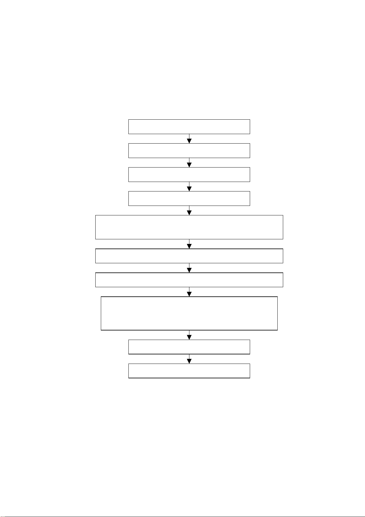
2. The alignment flow chart (see below figure)
Connect with central signal source, then check each function of TV such as
station missing, analog control etc., check the output of headphone and speaker
Input AV/SVIDEO signal, then check each function of all the terminals
Input HD signal (format), then check each function of the terminal
Input VGA, HDMI signal, check if the display is normal, check eac
function such as analog control etc., check horizontal /vertical center etc.
3. Description of adjustment
3.1 Unit adjustment
To produce digital board and analog board
Check the accessories and pack them in box
Check DDC and FLASH
All testing
Adjust white balance
Preset ex-factory
Fig-1 adjustment flow-chart
Connect the digital board, analog board, video processing board, button board and remote control
receiver board according to the wiring diagram 203-L27FB18-01JL or 203-L32FB18-01JL. Connect
with power and observe the display.
Method for using factory menu: press ”VOL” button to decrease the volume to 0, then press”9876”
to enter level one factory menu. Press ”CH+” and “CH-“ to select adjustment page, then press “OK”
3
Page 6

to access. Press “CH+” and “CH-“ to move cursor up and down, when the cursor stays on a certain
adjustment item, press “VOL-“ and “VOL+” to adjust. Press “MENU” exit to the level one factory
menu; press “EXIT” to exit from the factory menu at any situation.
Note: channel switch isn’t available at adjustment menu, only after return to level one factory menu,
you can switch channel.
3.2 adjustment of white balance
3.2.1 input 16 level gray-scale signal from VG849 to HDMI channel (TMIING: select a support
format of HDMI), enter white balance adjustment page of factory menu, select cool color
temperature of item, fixed WBGG_HDMI to 50H, adjust WBRG_HDMI, WBBG_HDMI, let the color
coordinate of third level on the right be (270,283) at 400nits; fixed WBBO_HDMI to 50H, adjust
WBRO_HDMI, WBGO_HDMI, let the color coordinate of third level on the left be (270,283) at 5nits.
The brightness of 400nits and 5nits may obtain by adjusting the contrast and brightness of menu.
3.2.2 input 16 level gray-scale signal from VG849 to AV channel (TMIING:968), enter white balance
adjustment page of factory menu, select cool color temperature of item, fixed WBGG_NTSC to 50H,
adjust WBRG_NTSC, WBBG_ NTSC, let the color coordinate of third level on the right be (270,283)
at 400nits; fixed WBBO_ NTSC to 50H, adjust WBRO_ NTSC, WBGO_ NTSC, let the color
coordinate of third level on the left be (270,283) at 5nits. The brightness of 400nits and 5nits may
obtain by adjusting the contrast and brightness of menu.
3.2.3 input 16 level gray-scale signal from VG849 to VGA channel (TMIING: select a support format
of VGA), enter white balance adjustment page of factory menu, select cool color temperature of
item, fixed WBGG_VGA to 128, adjust WBRG_ VGA, WBBG_VGA, let the color coordinate of third
level on the right be (270,283) at 400nits; fixed WBGO_VGA to 128, adjust WBRO_VGA,
WBBO_VGA, let the color coordinate of third level on the left be (270,283) at 5nits. The brightness
of 400nits and 5nits may obtain by adjusting the contrast and brightness of menu.
3.2.4 input 16 level gray-scale signal of 480I from VG849 to YPbPr channel, enter white balance
adjustment page of factory menu, select cool color temperature of item, fixed WBRG_YPbPr480I,
WBGG_YPbPr480I, WBBG_YPbPr480I to 128, and WBRO_YPbPr480I to 128, adjust
WBRO_YPbPr480I, WBBO_YPbPr480I, let the color coordinate of third level on the left be (270,283)
at 5nits. The brightness of 5nits may obtain by adjusting the contrast and brightness of menu.
Input format signals separately list on table 1, repeat the operation above until the white balance
pass muster.
Note: the white balance adjustment of VGA and YPBPR must be done at the situation that the white
balance adjustment of HDMI is accurate.
4 Performance check
4.1 TV function
Connect RF-TV terminal to the central signal source, enter the setup menu→ auto search, check if
there is station skipping, the output of earphone and speaker, the picture are normal.
4.2 AV/S-VIDEO terminal
Input AV/S signal, check if the picture and sound are normal.
4.3 YPbPr/YCbCr terminal
Input YUV signal (VG-849 signal generator), separate input YUV format signal of table 1 and check
if the picture and sound are normal.
Table 1 YUV signal format
No H-frequency (KHz) V-frequency (KHz) Signal
1 15.734 59.94 SDTV 480i
4
Page 7
2 31.469 59.94 HDTV 480p
3 44.955 59.94 HDTV 720p
4 33.716 59.94 HDTV 1080i
4.4 VGA terminal
Input VGA signal (VG-849 signal generator), separate input VGA format signal of table 2 and check
if the picture and sound are normal. If the image is deflection of the H-field, select manual correction
of Advanced Video Menu.
4.5 HDMI terminal
HDMI signal format receives the three high-definition signals: 480I, 480P, 720P/60Hz, 1080I/60Hz,
except for the table 2 signal. Check if the image (contain HDCP ON and OFF) and sound are
normal.
Table 2 VGA signal format
No Resolution H-frequency(kHz) V-frenquency(Hz)
1 720 X 400 31.469 70.086 28.322 IBM
2 640 X 480 31.469 59.94 25.175 IBM
3 640 X 480 37.861 72.809 31.5 VESA
4 640 X 480 37.5 75 31.5 VESA
5 640 X 480 43.269 85.008 36 VESA
6 800 X 600 35.156 56.25 36 VESA
7 800 X 600 37.879 60.317 40 VESA
8 800 X 600 48.077 72.188 50 VESA
9 800 X 600 46.875 75 49.5 VESA
10 800 X 600 53.674 85.061 56.25 VESA
11 1024 X 768 48.363 60.004 65 VESA
12 1024 X 768 56.476 70.069 75 VESA
13 1024 X 768 60.023 75.029 78.75 VESA
Point clock pulse
frenquency(MHz)
Remark
5 Ex-factory setting of user menu
1) Select TV channel, volume: 25
2) Video menu, Picture Mode: Nature, Aspect Ratio: Wide
3) Video menu, Advanced Video Menu:
Noise Reduction——Spatial: On
Noise Reduction——Speckle: Off
Noise Reduction——Temporal: On
Sharpness: 0
Tine: 50
Color Temperature: Cool
Skin Tome: White
Auto Contrast Enhancement: Off
Black Bar Detection: Off
3D Y/C: On
4) Audio menu, Sound Mode: News, Balance: 31, Earphone Vo1:31
5
Page 8
Digital Audio Output: AC-3, MTS: Mono
5) Setup menu, Tuning Band: Air
6) Feature menu, Sleep Timer: Off, Menu Language: English
Note: Except for Color Temperature of Cool, the Advanced Video Menu of YPBPR/YCBCR and
VGA channels sets according to the adjustment of factory.
Trouble shooting
Before servicing please check to find the possible causes of the troubles according to the table
below.
1.Antenna(signal):
Picture is out of focus or jumping Bad status in signal receiving
Poor signal
Check if there are failures with the electrical connector or
the antenna.
Check if the antenna is properly connected.
Fringe in picture Check if the antenna is correctly oriented.
Maybe there is electric wave reflected from hilltop or
building.
Picture is interfered by stripe
shaped bright spots
There appear streaks or light color
on the screen
2.TV set:
Symptoms Possible cause
Unable to switch the power on Check to see if the power plug has been inserted
No picture and sound Check to see if the power supply of liquid crystal TV has
Deterioration of color phase or
color tone
Possibly due to interference from automobile, train, high
voltage transmission line, neon lamp etc.
Maybe there is interference between antenna and power
supply line. Please try to separate them in a longer
distance.
Maybe the shielded-layer of signal wire is not connected
properly to the connector.
Check if interfered by other equipment and if interfered
possibly by the equipment like transmitting antenna, non
professional radio station and cellular phone.
properly into the socket.
been switched on. ( as can be indicated by the red LED
at the front of the TV set)
See if it’s receiving the signal that is transmitted from
other source than the station
Check if it’s connected to the wrong terminal or if the
input mode is correct.
Check if the signal cable connection between video
frequency source and the liquid crystal TV set is correct.
Check if all the picture setups have been corrected.
6
Page 9
Symptoms Possible cause
Screen position or size is not
proper
Picture is twisted and deformed Check to see if the picture-frame ratio is properly set up.
Picture color changed or colorless Check the “Component” or “RGB” settings of the liquid
Picture too bright and there is
distortion in the brightest area
Picture is whitish or too bright in
the darkest area of the picture
No picture or signal produced from
the displayer if “XXX in search”
appears.
There appears an indication “outside the receivable scope)
Remote control cannot work
properly
No picture and sound, but only
hash.
Blur picture Check if the antenna cable is correctly connected.
No sound Check if the “mute” audio frequency setting is selected.
When playing VHS picture search
tape, there are lines at the top or
bottom of the picture.
Check is the screen position and size is correctly set up.
crystal TV set and make proper adjustment according to
the signal types.
Check if the contrast setting is too high.
Possibly the output quality of DVD broadcaster is set too
high.
It maybe also due to improper terminal connection of the
video frequency signal in a certain position of the
system.
Check if the setting for the brightness is too high
Possibly the brightness grade of DVD player
(broadcaster) is set too high.
Check if the cable is disconnected.
Check if it’s connected to the proper terminal or if the
input mode is correct.
Check if the TV set can receive input signal. The signal is
not correctly identified and VGA format is beyond the
specified scope.
Check if the batteries are installed in the reverse order.
Check if the battery is effective.
Check the distance or angle from the monitor.
Check if there is any obstruct between the remote control
and the TV set.
Check if the remote control signal- receiving window is
exposed to strong fluorescence.
Check if the antenna cable is correctly connected, or if it
has received the video signal correctly.
Of if it has received the right video signal.
Check if the sound volume is set to minimum.
Make sure the earphone is not connected.
Check if the cable connection is loose.
When being played or in pause VHS picture search tape
sometimes can’t provide stable picture, which may lead
to incorrect display of the liquid crystal TV, In this case
please press “auto” key on the remote control so as to
enable the liquid crystal TV set to recheck the signal and
then to display correct picture signal
7
Page 10
Method of software upgrading
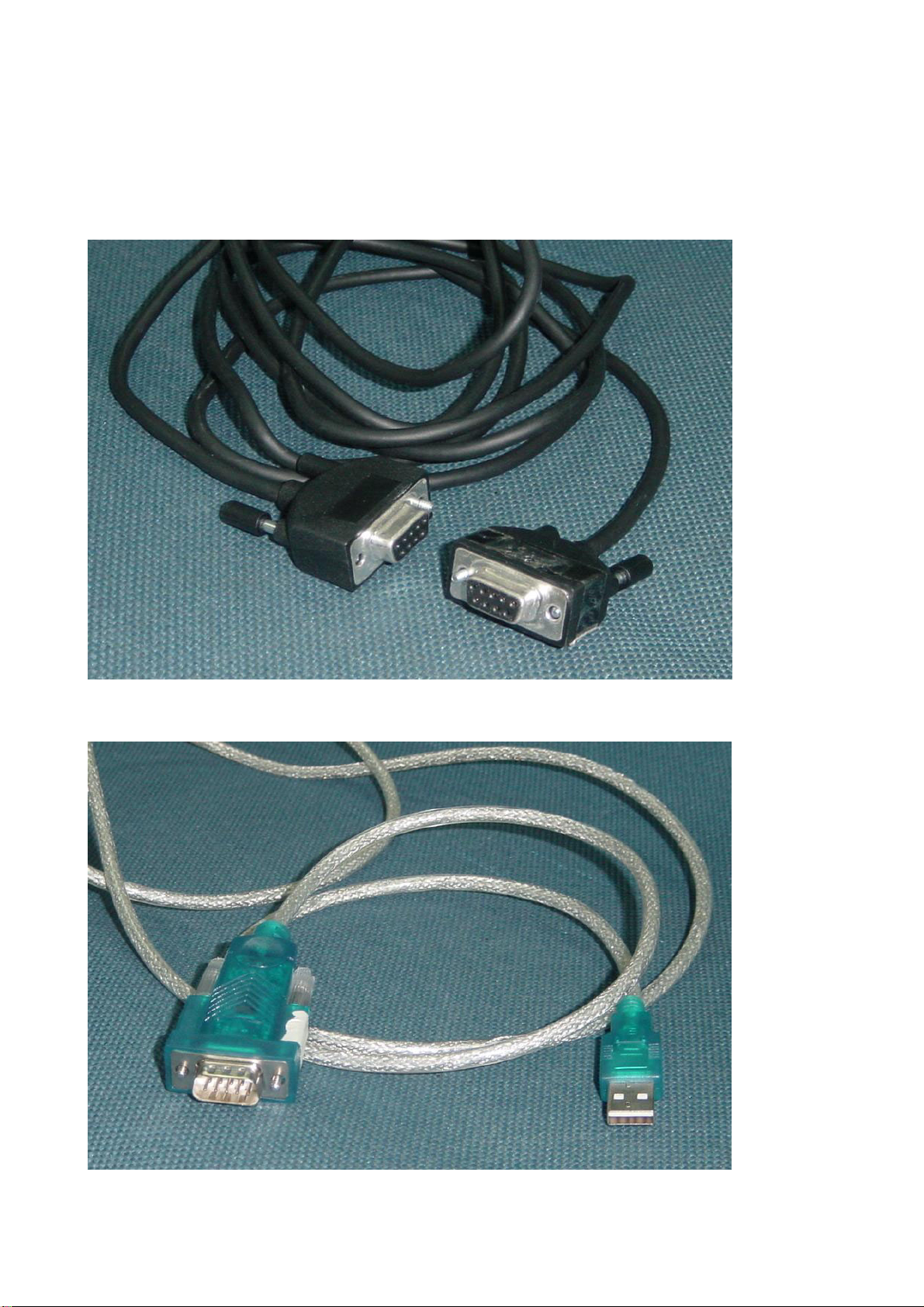
1. Connect RS-232 cable to computer and TV set. The cable must be a female to female RS-232
cable, and the line is TXD to RXD and RXD to TXD cross-link. It’s popular for PC to PC
connection.
2. If the computer has no RS-232 serial port(e.g. Notebook PC),you needs a additional USB to serial
port cable.
8
Page 11
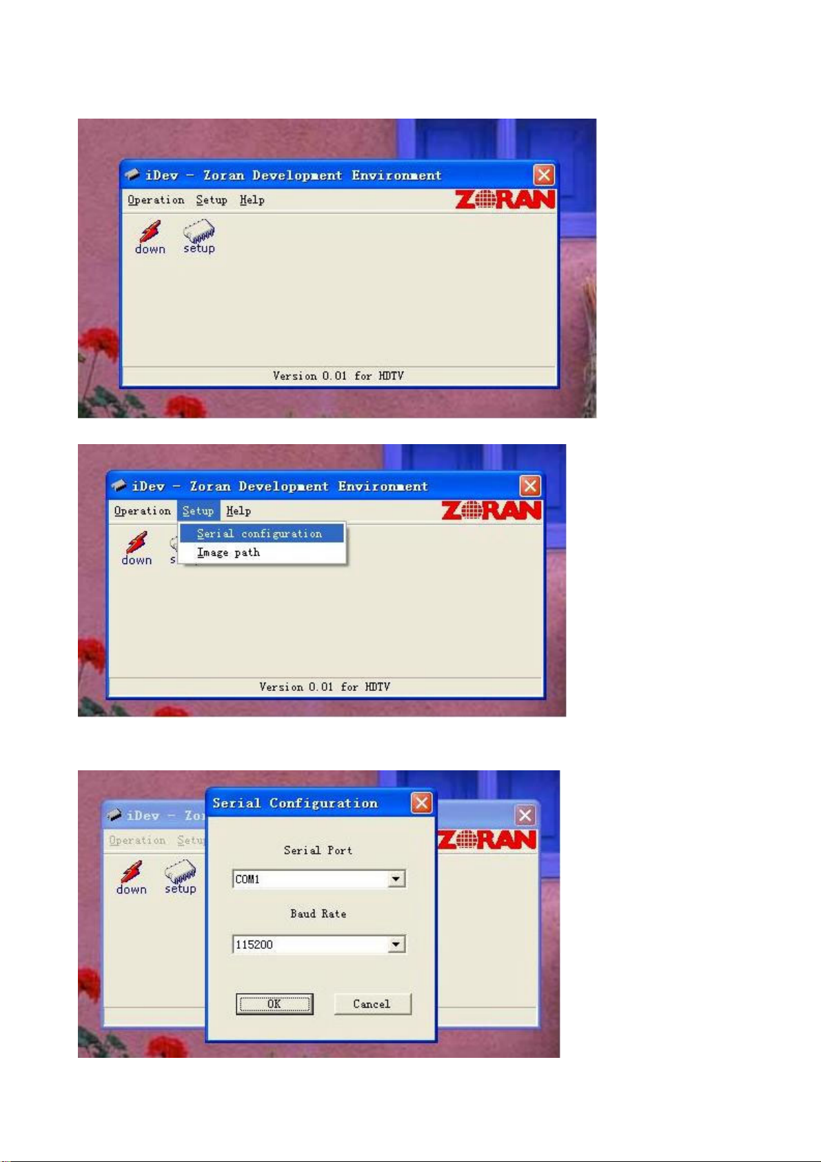
3. Copy the update tools (iDev.exe) to the path you want to do it, and double click it.
4. Select “setup” menu.
5. Confirm the Serial port is right. Base on the port which using for update. And set the band rate to
115200 (default).
9
Page 12
6. Select the “Image path” menu.
7. Confirm it’s the right file.
8. If it’s not right(Maybe you didn’t select it before),click the “…”button to select “*.ecc” file. Sometimes
the image file you got it will be “*.rar ”or “*.zip” zip file, needs unzip it first.
10
Page 13
9. You also can click the setup button to select and config, but please don’t select the red
one(update boot sector).
10. Then click the “down” button.
11
Page 14
11. You can see the “waiting” window.
12. Then power (off then) on the TV set.
13. After download, it will be burning.
12
Page 15

14. Last it will be finished
15. Press the (IR/ locate keypad) power key and holding for several second to force power off TV set,
then power on again. It would be ok now. If it’s failure you can try once again.
13
Page 16

Working principle analysis of the unit
1. NTSC signal flow:
Antenna reception NTSC signal send to the integrative tuner FQD1236, which contains HF and IF
amplifier circuit and video decoding circuit. It is controlled by main IC ZR39660 (inside CPU)
through I2C bus. The NTSC signal via frequency tuning, HF amplification, IF amplification, system
switching and decoding, output video signal TV-CVBS of 1Vpp and sound IF signal (SIF).
TV-CVBS and AV1-CVBS, AV2-CVBS input from AV terminal, via switch IC HEF4052 to output
signal, one way send to ZR39660 for VEDIO DECODER, DEINTERLACE and SCALER, then send
to LVDS level drive for LCD screen, another way is output through AV output socket as AV OUT.
The sound IF (SIF) is fed into demodulation IC CAS220, via decoding and A/D conversion, it is fed
into ZR39660 for analog control in the format of I2S. ZR39660 outputs audio data of I2S format, it is
fed into audio D/A converter IC CS4344, output analog L/R signal. The L/R signal and sound signal
of PC/YPRPB via diverter switch HEF4052BT, send to R2S15900SP (sound processing and volume
control). Select right/left sound channel, their send to digital sound amplifier TPA3001 amplify, then
send to speaker.
2. ATSC signal flow:
Antenna reception ATSC signal send to tuner FQD1236, after frequency tuning, HF amplification, IF
amplification and SAW FILTER, output IF signal to demodulation chip CAS220, via VSB or QAM
demodulation, Sound stereo decoder, fed to ZR39660 for information source decoding in the format
of standard serial TS stream.
HD video signal via decoding to A/D conversion and OSD superposition, at last send to LVDS drive
level for PDP panel.
HD audio signal, via decoder built-in ZR39660, resumed to multi- channel sound of Dolby AC-3, at
the same time output data stream of I2S format and S/PDIF data stream. Audio data of I2S format is
fed to audio D/A conversion chip CS4344 to output analog L/R signal. S/PDIF data stream directly
output from optical fiber interface.
3. PC/YPrPb signal flow
PC and two YPBPR signal via matched resistance, it a-c couple to video switch SN74CBT3257CDR,
via switching to selected signal to Triple Video A/D Converter MST9883 A/D conversion. Send
B/G/B of 24 bit to main IC ZR39660 digital decode, image scale and OSD superposition, then send
to LVDS level drive for LCD screen.
Sound signal (PC, YPrPb) via switch diverter HEF4052BT to output signal, it send to R2S15900SP
(sound processing and volume control) switch of audio. Select right/left sound channel, their send to
digital sound amplifier TPA3001 amplify, then send to speaker.
4. HDMI signal flow
HDMI video signal is directly fed to main IC ZR39660 (with HDCP function of HDMI) digital decode,
image scale and OSD superposition, then output LVDS drive level for screen.
HDMI audio signal, via decoder built-in ZR39660,output data stream of I2S format and S/PDIF data
stream at the same time. Audio data of I2S format is fed to audio D/A conversion chip CS4344 to
output analog L/R signal. S/PDIF data stream directly output from optical fiber interface.
14
Page 17
Block diagram
54321
PC
D
YPBPR2
YPBPR1
SN3257C
SN3257C
RGB/YUV
MST9883
M29W320E
HDMI
FLASH
2X16MX16
DDRAM
6
D
LVDS
24-BIT Data
HS,VS,CLK
TUNER
C
YPBPR1 AUDIO
YPBPR2 AUDIO
PC AUDIO
FQD1236 MK5
Digital IF
CAS220CS
ZR39660
BGA400
Analog SIF
JEPICO
j-L003
AV_OUT
Panel
C
SN3253C
CVBS_TV
CVBS1
CVBS2
S_Y
S_C
B
HEF4052BT
IIS IN
TS
CVBS,Y/C
B
IIS OUT
D/A CS4344
Loudspeaker
R2S15102NP
AV1 AUDIO
A
AV2 AUDIO
R2S15900SP
NJW1109
Earphone
A
LC-27FB26
V1.0
1 2 3 4 56
Page 18

IC block diagram
1. ZR39140
16
Page 19

Pin descriptions of ZR39660:
(1) Serial Transport Input Port
T4: MPEG Transport Port Input Clock
T3: MPEG Transport Input Data
U3: MPEG Transport Input Frame
Y1: MPEG Transport Input Valid
(2) HDMI Input
D1,E3,F3,E2,F2,E1: HDMI Differential Data Pairs
D2,C1: HDMI Differential Clock Pair
C3: HDMI Serial Clock
B2: HDMI Serial Data
A1: HDMI Hot Plug Detect
D3: HDMI Current Set
(3) NTSC/PAL Analog Input Port
W2:Video Front End Luminance In
Y3:Video Front End Chroma In
W3:Video Front End Common Mode Reference
(4) Analog Video Output
K18:Composite Data Output (CVBS)
J20:Blue/Pb Pixel Data Output
J18:Green/Y Pixel Data Output
J19:Red/Pr Pixel Data Output
(5) Audio I/O
R2:Audio Clock
R3:Bit Clock
P3:Left/Right Channel Selector
U2:Serial Audio Data Input
T2:Serial Audio Data Output
V1:IEC958 Format Out
(6) LVDS Panel Interface
B20,C19: Output Clock Pair
E18,F17: Output Data Pairs 0
C20,D19: Output Data Pairs 1
F18,G17: Output Data Pairs 2
D20,E19: Output Data Pairs 3
E20,F19: Output Data Pairs 4
H18,G18: Output Data Pairs 5
F20,G19: Output Data Pairs 6
G20,H19: Output Data Pairs 7
D18 : External Resistor Connection
17
Page 20

(7) UART and I2C Interface
N1: UART 0 Transmit
P1: UART 0 Receive
R1:I2C Compatible Clock 0
P2:I2C Compatible Data 0
M3:I2C Compatible Clock 1
M2:I2C Compatible Data 1
(8) Miscellaneous
M4, N3: Two pins required to support the 24.576 MHz crystal
N5: Power On Reset
L4: Infrared Receive
2. j-L003 (Higobashi)
The j-L003(Higobashi) LSI provides a variety of image quality adjustment functions designed to
produce sharp, well-defined coloration in personal computer LCD monitors and LCDTV screens, as
well as dot-matrix displays in rear projection TVs, PDPs, and other devices.
The image-enhancement functions built into the j-L003 use a proprietary color management
technology that makes it possible to produce images that are closer than ever to nature. The j-L003
also includes black-white stretch, brightness correction, horizontal edge enhancement, and gamma
correction functions: these expand your capabilities even farther, to enable you to achieve your own
custom image-processing methods.
18
Page 21

Pin configuration of j-L003:
(1) TTL SIGNAL INPUT
71: VS INPUT 72: HS INPUT 73: DE 76: CLK INPUT;
74, 78, 79, 80, 81, 82, 84, 93: RED Signal INPUT;
94, 95, 96, 97, 98, 99, 101, 102: GREEN Signal INPUT;
103, 104, 106, 107, 108, 109, 110, 111: BLUE Signal INPUT;
(2) TTL SIGNAL OUTPUT
65: VS OUTPUT 66: HS OUTPUT 67: DE 34: CLK OUTPUT
05, 06, 07, 08, 09, 10, 11, 13: RED Signal OUTPUT
14, 15, 16, 18, 19, 20, 21, 22: GREEN Signal OUTPUT
23, 24, 26, 27, 28, 29, 30, 31: BLUE Signal OUTPUT
(3) I/O CONTROL
148: RESET 151: SMMRSE 156: ADID0 157: ADID1
3. CAS220/CS
The CAS-220/CSO is a multi-standard demodulator and decoder for terrestrial and digital cable TV
reception. It is designed to support 8-VSB (Vestigial Side Band) in full compliance with ATSC Digital
Television Standards, ITU-T J.83 Annex B, and OpenCable™ Out-of-Band Signaling. The
CAS-220/CSO also demodulates analog BTSC and Korea A2 sound.
Its basic function is to recover the digital data encoded into the broadcast signal, which includes
video and sound program information and ancillary data service.
Pin configuration of CAS220/CS:
19
Page 22

Pin descriptions of CAS220/CS:
61: RESET_N
79, 80 oscillator
13 Select I2C address
16: I2C data for host communication with the tuner
18: I2C clock to the tuner
19: I2C clock from host
20: I2C data from/to host
93,94: Differential input for IF
96,97: Differential input for SIF
63: Digital Sound Word select (L/R select)
65: Digital Sound Serial data output
66: Digital Sound Serial clock.
17,30,46,62,74,82,84: Power Supply 3.3V
5,9,22,37,53,69,75,78,86,87,99: Power Supply 1.8V
6,7,15,23,33,35,45,55,60,70,73,76,77,81,83,85,88,91,92,95,98: Ground
20
Page 23

4. MST9883
MST9883 is a Triple Video A/D Converter with Clamps & Pixel Clock Synthesizer. The triple ADC
support 12 - 110 MHz Sampling Rate. It integrated 5-bit pixel clock phase adjustment for precise
sample timing control. It’s Output support 4:2:2 Format Mode and it can Pin Compatible with
AD9883A.
Block diagram of MST9883 is flow:
21
Page 24

Pin configuration of MST9883:
Pin descriptions of MST9883:
54: Red analog input
48: Green analog input
43: Blue analog input
49: Sync on Green analog input
38: External Clamp Input
30: Horizontal SYNC Input
31: Vertical SYNC Input
29: Hold PLL Frequency, do not track HSYNC
56: Serial Interface clock
57: Serial Interface data pin
55: Serial interface address pin
70-77: Red output data
2-9: Green output data
12-19: Blue output data
67: Output data clock
66: HSYNC output
64: VSYNC output
22
Page 25

39,42,45,46,51,52,59,62: Analog Power
26,27,34,35: PLL Power
11,22, 23, 69,78,79: Digital Output Power
1,10,20,21,24,25,28,32,36,40,41,44,47,50,53,60,61,63,68,80:Ground
5. R2S15900SP
R2S15900SP is an audio signal processor. It has MUTE and Volume/Tone control. It can support 5
input selector.
Pin descriptions of R2S15900SP:
2,27: AV1 AUDIO INPUT L/R
3,26: AV2 AUDIO INPUT L/R
4,25: DTV AUDIO INPUT L/R
5,24: EAR PHONE L/R
6,23: AV OUT L/R
11,19: AUDIO OUTPUT L/R
17,18:I2C SDA/SCL
28: Power Supply
12: Ground
23
Page 26

6. R2S15102NP 10Wx2ch(SE)/20Wx1ch(BTL) Digital Audio Power Amplifier
R2S15102NP is a Digital Power Amplifier IC developed for TV
R2S15102NP can realize maximum Power 10Wx2ch (VD=24V, THD=10%, SE) at 8Ω load.
It is possible to replace from the conventional analog amplifier system to the digital amplifier system
easily.
Pin Configuration
No. NAME I/O Description
1 OUT1 O Power Output pin #1
2 VD1 - Power supply pin for power output stage #2
3 STBYL I Stand-by control pin. When this is “L”, circuit current is reduced.
There is the pull-down resistor: 50K ohm(typ.).
4 PWM1 I PWM input pin #1 (for phase compensation)
5 IN1 I Analog input #1.The gain is depended on the external resistance.
6 CBIAS I/O A capacitor is connected so that it may not be influenced of power
supply change (Ripple Filter).
7 ROSC I Control pin for PWM carrier frequency
8 GND - GND pin for analog block
9 VREF I/O Capacitor connection pin for analog block reference voltage
source
10 PROT O Protection Timer pin. At protection mode, the output
becomes ”L”-level.
(The timing capacitor is connected)
24
Page 27

I SE operation Analog input #2(as same as IN1) 11 IN2
I BTL operation When this is connected to DVDD pin via the
resister, Reversed signal of OUT1 is output to
OUT2.
12 PWM2 I PWM input pin #2 (for phase compensation)
13 MUTEL I Mute control pin. When this is “L”, it becomes mute status.
14 VD2 - Power supply pin for power output stage #2
15 OUT2 O Power Output pin #2
16 VS2 - Ground pin for power output stage #2
17 HB2 I/O Capacitor connection pin for bootstrap
18 DVDD O Built-in power supply pin for internal digital block.
19 HB1 I/O Capacitor connection pin for bootstrap #1
20 VS1 - Ground pin for power output stage #!
25
Page 28

Wiring diagram:
To speake r
Pin1, 2 r ig ht a ud io c ha nn el
borad i nt er fa ce
Backl ig ht
CN2
X10 2
667- 27FB18- 53
667- L27W18- 09
IR boa rd
XA0 1
Anal og bo ard
X10 3 X 222
X22 1 X101 X 104
4 pins
XC0 2
XB01 XB03
XC0 1
X80 1
X80 5 X60 2 X80 2
Digt al bo ard
667- 27FB18- 69
XB0 1
3 pins
Butto n bo ar d 66 7- 3 2F B1 8- 05
8
1
X 0
112
X
3
1
1
X
4 pins
2pins
X8
3X
60
04
0
5
XA
LVDS 3 0 pi ns
5
60
X
8 pins
d
r
8- 4 0
3 pins
Powe r boa rd
X
29
1
X50 2
X50 3
X5
0
1
667- L27U25- 20
3 pins
7 pins
Pin3, 4 l ef t au di o ch an ne l
X2
93
e
7
6
6 F 1
boaVid
o
- 32 B
Power s wi tc h
To speake r
203- L27FB18- 01JL
26
Page 29

Identification criteria for the bright spot and dark spot of the LCD screen
Category Criteria
One single
spot
Bright
spot
Dark
spots
Total defected point ≤8 ≤7 ≤5 ≤4 /
Two
neighboring
spots
Tot a l N o. ≤5 ≤2 ≤5 ≤2 ≤3
One single
spot
Two
neighboring
spots
Tot a l N o. ≤6 ≤7 ≤5 ≤4 ≤10
15" 20" 22" 30" 40" 15" 20" 22" 30" 40"
≤5 ≤2 ≤5 ≤2 ≤3
≤2 ≤1 ≤2 ≤1 ≤1
≤6 ≤7 ≤5 ≤4 ≤10
≤2 ≤2 ≤2 ≤1 ≤5
Notes:
1. Definition of defected point (bright spot, dark spot): It is identified as a defected point if its area
exceeds 1/2 of a single picture element (R, G, B).
2. Definition of bright spot: It is identified as a bright spot if it is bright in the state of dark field and its
bright size remains unchanged
3. Definition of dark spot: It is identified as a dark spot if it is dark in the state of white field and its
dark size remains unchanged
4. Definition of two neighboring points: Defects of a group of picture elements (RB, RG, GB).
Quantity allowed Distance between two spots
≥15mm
≥15mm
≥10mm ≥5mm
27
Page 30

Troubleshooting guide
r
N
N
N
d
N
p
N
p
Yes, turn the unit on
If the picture of each channel
is normal?
If the sound of each channel is
normal?
(1) abnormal picture
a) Failure with resistor rows R839~R844 of image processing board, which may lead to lack of
b) Failure with resistor rows R825~R830 of image processing board, which may lead to lack of
c) A certain differential wire pair of LVDS of XA50 or X803(RX0+/-, RX1+/-, RX2+/-, RX3+/-)is
d) Failure with resistor rows RA18~RA25, which may lead to loss of corresponding color from
e) Failure with NB07,NA51 and their peripheral circuit, which may lead to picture abnormal of
f) Failure with N104, which may lead to picture abnormal of TV, AV1, AV2, S-VIDEO.
g) Failure with N803/N805/N806, which may lead to picture abnormal in all channels.
Begin
A red indicator
lights?
A blue indicator
lights?
Ye s
Display picture?
Ye s
color or color splash.
color or color splash.
abnormal, which may lead to lack of color or color splash.
the gray degree corresponding to the picture of channel HDMI.
PC, YPrPb and YCrCb.
o
o
o
o
o
Check power board , button board and powe
cord
Check if the pin1 of X602 in data processing
board is high level(+5V)? check V660/V661.
Check if the crystal in data processing boar
starts, DDR clock is correct?
Check the signal inputted from the channel to
in IC or IC and its peripheral circuit or the
output of LVDS is normal
Check the signal inputted from the channel to
in IC is normal or IC(R2S15900/TPA3001)
and its periphery is normal
28
Page 31

/
N
r
r
b
N
N
p
p
N
r
N
N
p
d
N
(2) no picture, no sound
Red
Check the color of indicato
light
Check the powe
oard
o sound
Refer to (3) checking
rocedure
(3) with picture but no sound
With picture but no sound
Check if the voltage of sound amplifie
of X106 in analog board is normal?
Check if the pin5, pin11 of
111 inputs signals
Ye s
Check N111 and their
eripheral circuit
o picture, no sound
Ye s
o picture
Refer to (4) checking
rocedure
Ye s
Blue
Check the output voltage of
sockets X601~X604
Power board problem
o
Check the power board
o
Check N103/NB05 an
their peripheral circuit
X606/X608
o
29
Page 32

N
N
N
d
p
R
t
N
(4) with sound but no picture
Ye s
If there is no picture
in all channels?
Ye s
Check N108 an
its peripheral
circuit
With sound but no picture
Display OSD MENU?
Ye s
Display LOGO? If pin5 of X602 (IRR) has signal?
o
Check if the crystal in data processing board starts,
DDR clock and DDR SDRAM are normal?
o
Refer to (6), (7), (8), (9), (10),
(11), (12) checking procedure
Ye s
Refer to (5) checking
rocedure
o
o
Check N801, N802, DD
and their peripheral circui
and power supply
30
Page 33

(5) Check image processing board
y
N
N
f
N
N
r
N
d
p
d
p
Check the power suppl
of N803
Ye s
o
Check if pin20, 21, 27,
30 of X801is high level
Check if the power supply of
L801/L802 are normal
Ye s
o
Check if pin3, 5, 26 of N806
output H/V-SYNC and clock
Check the peripheral and power supply o
801, N802, DDR of data board
o
Ye s
Check the peripheral and powe
supply of N806
Check if pin34, 65, 66 of N803 output
H/V-SYNC and clock
o
Ye s
Check the peripheral an
ower supply of N803
Check the peripheral an
ower supply of N805
Note: please make sure that the data of FLASH N804 is correct before checking the image
processing board.
31
Page 34

(6) AV no picture
N
N
t
p
N
N
f
N
t
t
p
Check if pin13 of N104
outputs signals?
Ye s
Check the periphery circui
from XC02 to N801
(7) S-terminal no picture
Check if pin13/3 o
104 outputs signals?
Ye s
Check the periphery circui
from XC02 to N801
Check if C136 and C137
input signals?
Ye s
o
Check if C105 and C138
input signals?
Ye s
o
o
Check N105/N106 and the circuit
from AV terminal to N104
Check N104 and its
eriphery circuit
o
Check N108 and the circui
from S-terminal to N104
Check N104 and its
eriphery circuit
32
Page 35

(8) NTSC channel no picture
N
N
t
p
N
N
f
N
f
d
p
Check if pin11 of TUNER226
output signals?
Ye s
o
Check if pin13 of N104
outputs signals?
Check TUNER226 power supply
and the peripheral circuit.
Ye s
o
Check the periphery circui
from XC02 to N801
Check N104 and its
eriphery circuit
(9) ATSC channel no picture
Check if pin6/7 of TUNER226
output signals?
Ye s
o
Check if the crystal o
228 (20MHz) is normal?
Check TUNER226 power supply
and the peripheral circuit.
Ye s
o
Check the clock signal o
each pin of XC01
Check G226, N228 an
eriphery circuit
Note :
The I2C bus line control of TUNER is switch through the bus line of N228, so after checking the power
supply and peripheral circuit of TUNER226, it is still no picture in NTSC and ATSC channel, please
check N228 emphatically.
33
Page 36

(10) YprPb or Ycrcb channel no picture
N
f
N
N
N
m
N
f
N
N
m
Check if pin4/7/9 of NB07
output signals?
Ye s
Check if pin64/66/67 o
A51 are normal?
Ye s
o Ye s
Check resistor
rows RA63~
RA68
Check NA51
and peripheral
circuit.
(11) D-sub channel no picture
Check if pin4/7/9 of NB07
output signals?
Ye s
Check if pin64/66/67 o
A51 are normal?
Ye s
o
Check resistor
rows RA63~
RA68
Check NA51
and peripheral
circuit.
o
Check if pin4/7/9 of NB08 output
signals?
Check NB01/NB02
and the circuit fro
X807/X808 to N808
o
Check NB03/NB04
and the circuit fro
X807/X808 to N808
Check NB07
and peripheral
circuit.
o
34
Page 37

(12) HDMI channel no picture
p
N
f
p
p
N
p
f
N
y
p
NNN
Check DETECT NA04 and its
eripheral circuit?
Ye s
o
Check if signals o
RA18~RA25 are normal?
Ye s
Check N801 and its
eripheral circuit
Check the connection to HDMI
socket, NA04 and its
eripheral circuit
Note: N801 embeds FLASH, which stores DDC and HDCP information of HDMI, so make sure the
connection between HDMI socket/interface and the bus line is well- going, the picture will display.
(13) Troubleshooting guide of power supply board (23” and 27”)
a. No power supply
o power supply
Does AC voltage at C505
Y
Check if X501 FU501 is
roperly inserted?
Does DC voltage at C528
(150~370V)
Y
Check D502, R531, D508
Check if the 15V DC o
501 (pin13)
Y
Check N501 or peripheral
circuit
Check supplementar
ower supply
35
Page 38

b. No DC voltage output
N
N
N N
o DC voltage output
Check if DC voltage of C536 is
3.3V(5V)
Y
Check if DC voltage of V505 B
is 24V
Check N502 or peripheral
circuit
Check main board
Y
Check if DC voltage of C537 is
24V
Y
Check FU502
Check D515 or T501
36
Page 39

Page 40

Page 41

Page 42

Page 43

Page 44

Page 45

Page 46

Page 47

Page 48

Page 49

Page 50

APPENDIX-A: Main assembly list
Model Part No. Description
203.L27FB18-13 667.L27W18-09 IR receive board
667.L27W18-14 Indicator light board
667.32FB18-52 Image processing board
667.32FB18-05 Key board
667.32FB18-40 Video processing board
667.27FB26-20 Power board
667.27FB26-53 Analog board
667.27FB18-69 Data processing board
301.D42FB6-10A Remote control
335.27003-00 Panel
203.L32FB18-15 667.L32W18-09 IR receive board
667.L32W18-14 Indicator light board
667.32FB18-52 Image processing board
667.32FB18-05 Key board
667.32FB18-40 Video processing board
667.32FB26-20 Power board
667.32FB26-53 Analog board
667.32FB18-69 Data processing board
301.D42FB6-10A Remote control
335.32012-00 Panel
Page 51

APPENDIX: Exploded view (LC-27X18)
Page 52

PART LIST OF EXPLODED VIEW (LC-27X18)
No. PART NO. DESCRIPTIONRE
1 742-30091-00 Line clasp
2 615-10559-00 Stand assy
3 808-10829-00 Bottom connecting cover
4 808-10835-00 Rear cabinet(left)
5 870-10276-00 Connecting piece of speaker box
6 808-10837-00 Side decorate cover
7 808-10836-00 transfer axis cover
8 808-10812-00 Power lead cover
9 615-10545-00 Mounting assy
10 808-1A841-00 AV baffle (left)
11 Digital processing board assy
12 808-10840-00 Button cover
13 743-1B180-00 Button decorate piece
14 Button board assy
15 615-1A526-00 LCD screen fixed mount assy
16 Screen
17 808-2A330-202 ACTIVE panel
18 780-X18W0-00 Front cover
19 Power board assy
20 Sound trans-connecting assy
21 808-1A842-00 AV baffle (right)
22 Video processing board assy
23 Indicator assy
24 870-3A183-00 USB bracket
25 700-60255-00 LED column
26 Infrared receiving board assy
27 870-10285-00 Power supply socketbracket
28 780-X18RH-00 Rear cabinet
29 615-20464-00 Bottom speaker assy
Page 53

APPENDIX: Exploded view (LC-32X18)
Page 54

PART LIST OF EXPLODED VIEW (LC-32X18)
No. PART NO. DESCRIPTIONRE
1 808-20332-202 ACTIVE panel
2 780-G18L0-AW1 Front cover
3 870-30190-00 LED columnbracket
4 360-30042-00 Power switch
5 700-60256-00 LED column
6 700-60255-100 LED column
7 Infrared receiving board assy
8 Screen
9 615-10562-00 LCD screen fixed mount assy
10 Power board assy
11 Sound trans-connecting assy
12 870-10219-00 Mounting holder
13 808-10867-AF0 Rear cabinet (USB)
14 808-10865-AF0 Rear cabinet (right)
15 780-G18L1-AF1 Rear cabinet
16 808-10812-AF0 Power lead cover
17 615-20482-00 Bottom speaker assy
18 615-10578-00 Stand assy
19 808-10863-AF0 Speaker connecting cover
20 808-10866-AF0 Rear cabinet (bottom )
21 808-10864-AF0 Rear cabinet (left)
22 808-10859-AF0 decorate cover (leftright)
23 Button board assy
24 870-10218-00 Mounting holder (horizontal )
25 870-1A133-00A Mounting holder (middle )
26 CPU board assy
27 Video processing board assy
Page 55

603-L27FB18-13
Ver.1.0
 Loading...