

Page 1
COLOR TELEVISION
LC22K9
Page 2

CONTENT
Safety instructions………………………………………………………………………..…
Instructions on adjusting and testing…………………………….…….…………………
Trouble shooting……………………………………………………….……………………
Principle analysis of LC-22K9……………………………………….………..………….
LC22K9 BLOCK DIAGRAM…………………………………………………………………0
Wiring diagram……………………………………………………………..……………....
Components No…………………………………………………………………………….…
Identification criteria for the bright spot and dark spot of the LCD screen………..….
Troubleshooting guide………………………………………………………………..……
Exploded views…………………………………………………………………………..…
Schematic diagram…………………………………………………………………….…..
1
3
6
9
10
15
16
17
18
21
23
Page 3

Attention: This service manual is only for service personnel to take reference with. Before servicing
please read the following points carefully.
Safety instructions
1. Instructions
1.1 Be sure to switch off the power supply before replacing or welding any components
or inserting/plugging in connection wire
1.2 Anti static measures to be taken (throughout the entire production process!):
a)Do not touch here and there by hand at will;
b) Be sure to use anti static electric iron;
c) It’s a must for the welder to wear anti static gloves.
1.3 Please refer to the detailed list before replacing components that have special
safety requirements. Do not change the specs and type at will.
2. Points for attention in servicing of LCD
2.1 Screens are different from one model to another and therefore not interchangeable. Be sure to use
the screen of the original model for replacement.
2.2 The operation voltage of LCD screen is 700-825V. Be sure to take proper measures in protecting
yourself and the machine when testing the system in the course of normal operation or right after the
power is switched off. Please do not touch the circuit or the metal part of the module that is in
operation mode.
Relevant operation is possible only one minute after the power is switched off.
2.3 Do not use any adapter that is not identical with the TV set. Otherwise it will cause fire or damage
to the set.
2.4 Never operate the set or do any installation work in bad environment such as wet bathroom,
laundry, kitchen,or nearby fire source, heating equipment and devices or exposure to sunlight etc.
Otherwise bad effect will result.
2.5. If any foreign substance such as water, liquid, metal slices or other matters happens to fall into the
module, be sure to cut the power off immediately and do not move anything on the module lest it
should cause fire or electric shock due to contact with the high voltage or short circuit.
2.6. Should there be smoke, abnormal smell or sound from the module, please shut the power off at
once. Likewise, if the screen is not working after the power is on or in the course of operation, the
power must be cut off immediately and no more operation is allowed under the same condition.
2.7. Do not pull out or plug in the connection wire when the module is in operation or just after the power
is off because in this case relatively high voltage still remains in the capacitor of the driving
circuit.Please wait at least one minute before the pulling out or plugging in the connection wire.
2.8. When operating or installing LCD please don’t subject the LCD components to bending, twisting or
extrusion, collision lest mishap should result.
1
Page 4
2.9 As most of the circuitry in LCD TV set is composed of CMOS integrated circuits, it’s necessary to pay
attention to anti statics. Before servicing LCD TV make sure to take anti static measure and ensure
full grounding for all the parts that have to be grounded.
2.10.There are lots of connection wires between parts behind the LCD screen. When servicing or
moving the set please take care not to touch or scratch them. Once they are damaged the screen
would be unable to work and no way to get it repaired.
2.11. Special care must be taken in transporting or handling it. Exquisite shock
vibration may lead to breakage of screen glass or damage to driving circuit.
Therefore it must be packed in a strong case before the transportation or
handling.
2.12. For the storage make sure to put it in a place where the environment can be controlled so as to
prevent the temperature and humidity from exceeding the limits as specified in the manual. For
prolonged storage, it is necessary to house it in an anti-moisture bag and put them altogether in one
place. The ambient conditions are tabulated as follows:
Temperature Scope for
0---+50 C
operation
Scope for
- 20----60 C
storage
humidity Scope for
20%---85%
operation
Scope for
10%---90%
storage
2.13. Display of a fixed picture for a long time may result in appearance of picture residue on the screen,
as commmonly called “ghost shadow”. The extent of the residual picture varies with the maker of
LCD screen. This phenonmenon doesn’t represent failure. This “ghost shadow” may remain in the
picture for a period of time (several minutes).But when operating it please avoid displaying still
picture in high brightness for a long time.
3.Points for attention during installation
3.1. The front panel of LCD screen is of glass. Wheng installing it please make sure to put it in place.
3.2. For service or instatallation it’s necessary to use specified screw lest it should damage the screen.
3.3. Be sure to take anti dust measures. Any foreign substance that happens to fall down between the
screen and the glass will affect the receiving and viewing effect
3.4. When dismantling or mounting the protective partition plate that is used for anti vibration and
insulation please take care to keep it in intactness so as to avoid hidden trouble.
3.5. Be sure to protect the cabinet from damage or scratch during service, dismantling or mounting.
2
Page 5

Instructions on adjusting and testing
The adjustment of LC22K9 excludes 2.30
2.1 Adjusting and calibrating the equipment
PM 5518(video frequency signal generator), K-7253(VGA signal generator),CA210(white balancer)
2.2 Adjustment and calibration procedure
2.3 Adjusting and calibrating the monitor board
Place the monitor board on the testing jig, turn on the power supply and switch on the set to see if it
is normal.
2.3.1 Adjusting the white balance of monitor board
Push the “Rest” key and “OK” key under the cover of the remote control set, repeat the push, enter
the factory menu. Select factory reset to initialize the MONITOR
Input the DVI signal to monitor board. (K-7253 time339 pattern 630 8 gray degree signals, input the
DVI signal to socket with 26 cores of monitor board by way of patch panel). Adjust the intermediate
second and seventh gray degree with CA210 white balancer. Preset value of R,G,B CUT to
100,and R,G,B DRV to 150, then, adjust the second gray degree (brightness: about 9nit) by R,G,B
CUT, to set the color coordinates of second gray degree to 270, 283. Adjust R,G,B DRV to set the
color coordinate of seventh gray degree to 270 and 283.
Note: Because the values of R,G,B CUT and R,G,B DRV directly determines the values of
brightness and contrast at the DVI terminal of monitor board, the white balance should be
adjusted according to the preset value strictly. The value after adjusting should be within
+/-10 of the preset value.
2.3.2 Calibrating ADC of Monitor
After finishing the adjustment of 2.3.1, set the VGA signal to 1024X768 60Hz mode. Access the
pane signal and connect it to VGA terminal of monitor. Adjust h port of the picture to make the
picture fully occupy the screen. Enter the factory menu and select items for ADC calibration and
calibrate the ADC according to the indication on the screen.
2.3.3 Adjusting the white balance of monitor:
Input 8 gray degree signals of 1024X768 60Hz mode, push “display” key on the remote control
set, adjust brightness and contrast, to set the brightness of second gray degree to 5nit and
seventh as 400nit.
For the diagram of adjustment and calibration procedure, see diagram 1
3
Page 6
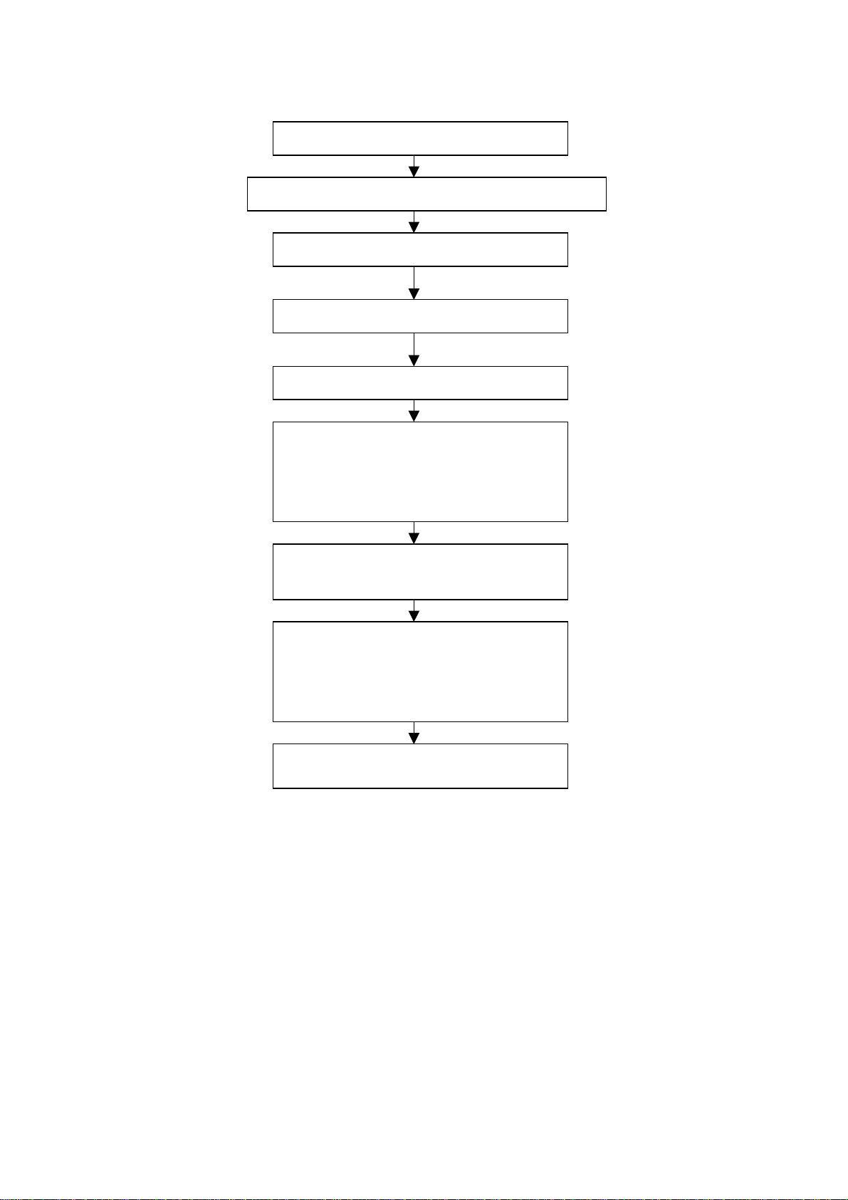
V
y
r
k
f
d
d
B CUT and B DRV is fixed as 128. Adjust R G CUT,to make second degree of the color
coordinate as 270 283. Adjust R G DRV to set seventh degree of the color coordinate to 270
283. Adjust R G CUT and R G DRV again and again, until both of the two gray degrees are at
270 and 283.
2.4 Connect decoder board and push button board with the monitor board verified to be normal
(LC-30K9/LC40K9 power is as per connection diagram 203-L30K90-01JL whereas LC-22K9 is as
per 203-L22K90-01JL). After power on, observe if the display is normal.
Method to enter factory menu: Continuously push key of “VOL+” “Mute”, “Video” to enter factory
menu. When the first line of each and every adjusting item is in the highest brightness push
Production of the main board and decoders on the line
General assembly and combined calibration
Connect central signal source, check T
functions (station skipping, analog quantit
control etc) . Check if the output of speake
is normal
Input AV/S and HDTV signal and chec
following functions of the terminals
Input VGA signal (one format), check i
display is normal under the PC status, an
functions (analog control), central of line an
field etc.
Check accessories, then packing
Figure 1. Adjustment and calibration procedure
Check if FLASH is written
Check Monitor board
Check decoders in media board
4
Page 7

“ENTER” key to select different adjustment items. When VGA and DVI are input, select “mode”
and then push “ENTER” key and select three color temperatures 6500K,9300K,12000K. Push
“MENU” to quit factory menu.
Notice: Adjustment of Media Box must be performed under the mode --”Nature” of picture.
2.4.1 EPROM Initialization
Enter the first page of factory menu, select clear eprom and push “ENTER” key, shut off the set after
the appearance of “OK”.
2.4.2.Adjustin VGA and DVI channel
2.4.2.1 Presetting the VGA channel mode
Input VGA signal from K-7253 (PATTERN 5),select IME301,push “AUTO” to automatically adjust the
picture to be in full screen. Also auto-adjust
TIME302,TIME303,TIME311,TIME313,TIME315,TIME316,TIME317,TIME319,TIME339
respectively.
2.4.2.2 Adjusting ADC of VGA channel
Input K-7253 TIME311,PATTERN474 64 degree of gray signal, adjust adc-gain to maximum (no
bigger than 20), and to set two neighboring brightest degrees distinguishable.
2.4.2.3. Adjusting white balance of VGA and DVI channel
Input eighth degree of gray signal K-7253 TIME311 and PATTERN471, enter adjustment menu of
white balance, and use white balancer to adjust second and seventh degree of gray signal.
Select mode to be 6500K, adjust offset_R,offset_G,offset_B, to set second color coordination to 313
293 and the brightness to about 5nit.Fix gain_R as 128, adjust gain_G,gain_B to set seventh color
coordination to 313 293. Adjust offset_R,offset_G,offset_and gain_G,gain_B,again and again until
two gray degrees are 313 and 293.
Selct mode to be 9300K, adjust offset_R,offset_G,offset_B, to set second color coordinate to
281,311 and the brightness to about 5nit.Fix gain_G as 128, adjust gain_R,gain_B to set seventh
color coordinate to 281, 311.Adjust offset_R,offset_G,offset_and gain_R,gain_B,again and again
until two gray degrees are 281 313.
Select mode to be 12000K, adjust offset_R,offset_G,offset_B, to set second color coordinate to 270
283 and the brightness to about 5nit.Fix gain_B as 128, adjust gain_R,gain_B to set seventh color
coordinates to 270, 283. Adjust offset_R,offset_G,offset_B and gain_R,gain_G,again and again until
two gray degrees are 270 283.
Notice: The value of gain_R,gain_G,gain_B should not exceed 128.
2.4.3. Adjusting TV channel
2.4.3.1. Adjusting sub-brightness and sub-contrast of VCO and OPTION
Input AV color bar signal (PM 5518 COLOUR BAR 100%) to terminal of VIDEO 1, enter the first
page of factory menu, select auto color, push”ENTER”key. After two seconds, display of OK shows
the completion of adjustment. Adjust the value of Option to 9, S-brightness to 124,and S-contrast
140.
2.4.3.2 Adjusting white balance of TV channel
Input AV signal, (PM 5518 gray signal ),enter the adjustment menu of white balance, adjust second
and seventh degrees by white balancer. Adjust offset_R,offset_G,offset_B, set the second color
coordinate to 270 283 and the brightness to about 5nit.Fix gain_R as 133, adjust gain_R gain_G to
set the seventh color coordinate to 270 283.Adjust offset_R,offset_G,offset_B and
gain_R,gain_G,again and again until two gray degrees are 270 283.
5
Page 8

2.4.4 Adjusting white balance of YPbPr channel
Input YPbPr signal of K-7253 to terminal of YPbPr, input 8 gray degree signal to
TIME380(480i)PATTERN471, adjust S-brightness to 20,and S-contrast 140.
Enter adjustment menu of white balance, adjust second degrees by white balancer. Adjust
offset_R,offset_G,offset_B to set the second color coordinate to 270 283 and the brightness to about
5nit.
Separately input the eighth degree of gray signals of TIME392(480p),TIME394(720p)and
TIME396(1080i)mode. Repeat the above operation so that the second color coordinates are 270
283 and the brightness about 5nit.
3. Functional inspection
3.1 TV function
Enter search menu---auto search, connect central signal to RF terminal and check if there is missing
of station.
Input A21 signal and check the function of CCD.
3.2 AV/S HDTV terminal
Input HDTV signal to AV/S, and check if it is normal.
3.3 VGA connector
Insert VGA signal connector, input 640 x 480@60 Hz VGA format signal, and check if display is
normal. If there is interfere on the picture, push the auto-adjust key on the remote control set once
more, check if the display is normal.
3.4 Inspection of PCMCIA channel
Insert PCMCIA card, switchover to this channel, and check if the display is normal.
3.5 Inspecting sound channel
Inspect if the output of speaker and earphone of channels is normal.
Trouble shooting
Before servicing please check to find the possible causes of the troubles according to the table below.
1.Antenna:
Picture is out of focus or jumping Bad status in signal receiving
Maybe broadcast signal itself is not good
Check if the outdoor antenna is disconnected.
Check if the antenna is correctly oriented.
Fringe in picture Check if the antenna is correctly oriented.
Maybe there is electric wave reflected from hilltop or building.
Picture is interfered by stripe
shaped bright spots
There appear streaks or light color
on the screen
Possibly due to interference from automobile, train, high
voltage transmission line, neon lamp etc.
Maybe there is interference between antenna and power
supply line. Please try to separate them in a longer distance.
Check if interfered by other equipment and if interfered
possibly by the equipment like transmitting antenna, non
professional radio station and cellular phone.
6
Page 9
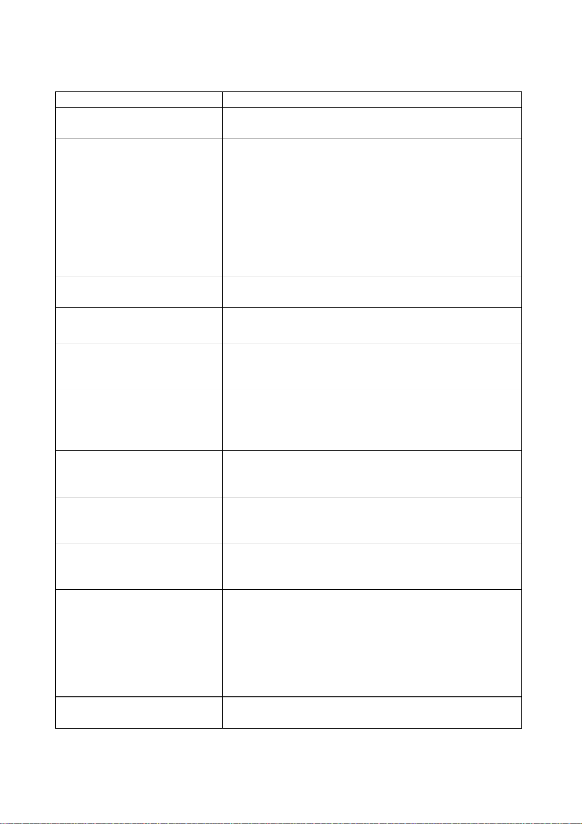
2.TV set:
Symptoms Possible cause
Unable to switch the power on Check to see if the power plug has been inserted properly into
the socket.
No picture and sound Check to see if the power supply of liquid crystal TV has been
switched on. (as can be indicated by the red LED at the front
of the TV set)
See if it’s receiving the signal that is transmitted from other
source than the station
Check if it’s connected to the wrong terminal or if the input
mode is correct.
Check if the signal cable connection between video frequency
source and the liquid crystal TV set is correct.
Deterioration of color phase or color
tone
Screen position or size is not proper Check is the screen position and size is correctly set up.
Picture is twisted and deformed Check to see if the picture-frame ratio is properly set up.
Picture color changed or colorless Check the “Component” or”RGB”settings of the liquid crystal
Picture too bright and there is
distortion in the brightest area
Picture is whitish or too bright in the
darkest area of the picture
No picture or signal produced from
the displayer if “XXX in
search”appears.
There appears an indication “outside the receivable scope)
Remote control cannot work
properly
No picture and sound, but only
hash.
Check if all the picture setups have been corrected.
TV set and make proper adjustment according to the signal
types.
Check if the contrast setting is too high.
Possibly the output quality of DVD broadcaster is set too high.
It maybe also due to improper terminal connection of the video
frequency signal in a certain position of the system.
Check if the setting for the brightness is too high
Possibly the brightness grade of DVD player(broadcaster)is
set too high.
Check if the cable is disconnected.
Check if it’s connected to the proper terminal or if the input
mode is correct.
Check if the TV set can receive input signal. The signal is not
correctly identified and VGA format is beyond the specified
scope.
Check if the batteries are installed in the reverse order.
Check if the battery is effective.
Check the distance or angle from the monitor.
Check if there is any obstruct between the remote control and
the TV set.
Check if the remote control signal- receiving window is
exposed to strong fluorescence.
Check if the antenna cable is correctly connected, or if it has
received the video signal correctly.
7
Page 10
Blur picture Check if the antenna cable is correctly connected.
Of if it has received the right video signal.
No sound Check if the “mute” audio frequency setting is selected.
Check if the sound volume is set to minimum.
Make sure the earphone is not connected.
Check if the cable connection is loose.
When playing VHS picture search
tape, there are lines at the top or
bottom of the picture.
When being played or in pause VHS picture search tape
sometimes can’t provide stable picture, which may lead to
incorrect display of the liquid crystal TVIn this case please
press “auto” key on the remote control so as to enable the
liquid crystal TV set to recheck the signal and then to
display correct picture signal
8
Page 11

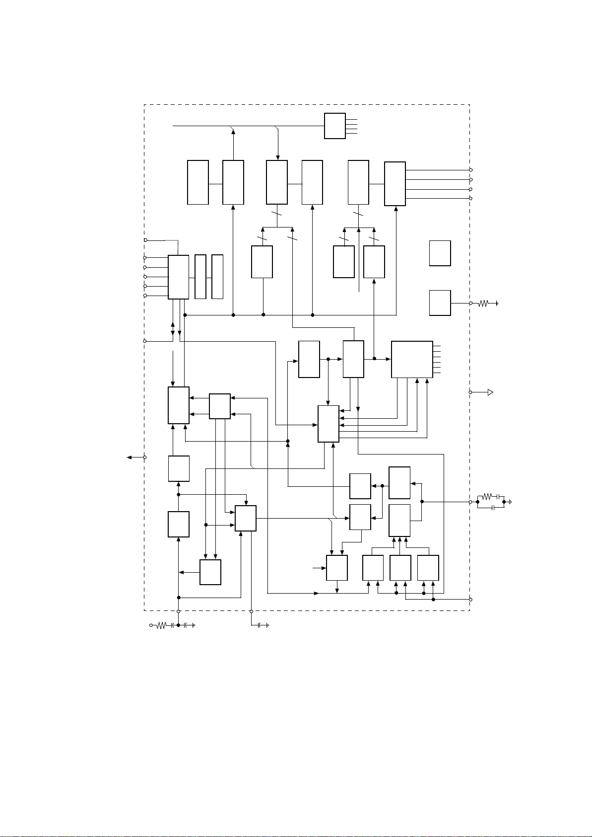
Principle analysis of LC-22K9
For the working principle of LC-22K9 please refer to LC-22K9 block diagram of the complete TV set.
Following is a short description of the signal flow:
RF signal through an integral tuner TUNER201 produces complete color TV signal which is input,
together with AV1/SVHS(SVHS in priority)AV2 and PCMCIA video signals, into U29 VPC3230D for
conversion selection and decoding. Except for being decoded the selected video signal is divided in two
routes: one is fed to AV output terminal and another route of signal to special 21 line decoder U32
Z86229 of CCD/V-CHIP for decoding. After decoding by U32, the signal is sent back to U29 with
R,G,B,FB format and superimposed to the original picture decoded, then sent to U13 FLI2310 in
ITU-R656 of 8B1T format for progressive line processing.
YPbPr signal, after analog to digital conversion by U30 MST9883 into YUV with 24BIT is also sent
to FLI2310.
Above two routes of signal are processed by FLI2310 for matrix, color density and tint and then
output as RGB with 24 BIT into the main processor chip U12 JAG-ASM. There are other two routes of
signals: one route is RGB signal of VGA for computer, another route is DV1 into RGB signal with 24 bit to
U12 through interface of U15 TFP403/501. Three routes of signal are processed in U12 for picture
format. Among them, one route of VGA after A/D conversion for RGB is subject to selection for
conversion, together with other two routes, and then processed for digital display including OSD AND
GAMMA correction, and brightness and contrast processing and changed into 1024*768 format. The
RGB signal with 24BIT is output to the LVDS converter, U31 DS90C383A, for conversion into the
signal format which the screen can accept, that is, three pairs of low voltage differential signal and one
pair of time signal. And they are further sent to LCD screen for picture display. The PWM of U12 is also
used to control the brightness of the background light.
The second sound IF signal SIF output from tuner is sent to sound frequency processor N201
MSP3420; the sound frequency signal of YPRPB,DVI and PCMCIA is also sent to N201 after switching
over and selection by switch U34 HEF4052. The AV1/SVHS,AV2 and VGA audio signal are also sent to
N201 respectively, where the second sound IF SIF is first demodulated to the audio signal which,
together with four way audio signal, is selected for conversion, and then further sound magnitude
controlled and sound effect treated. The output of left and right signal R/L is divided into two routes: one
is sent to SRS sound field processor N203 M62494 for SRS surrounding sound processing, and further
used to drive the speaker after the D-type sound power amplification N207 LX1722 and
amplification of N205,N206,N208,N210 SI4532DY; the other route is used to drive earphone after
power amplification N212 TLE2142.
Power is supplied from power adapter and then converted into the power required by various
channels and circuits.
9
Page 12
LC22K9 BLOCK DIAGRAM
VGA
DVI
RF
AV1-V/S-Y
SVHS-C
AV2-V
PCMCIA-YUV
AV-V OUT
YPrPb
U15 DVI
receiver
TFP403/501
TUNER201
VIDEO DECODER
VPC3230
U32
CCD
V-CHIP
Z86229
U30
ADC
MST9883
V
U29
FBV
RGB
RGB
SIF
ITU-R656
8bit
24bit
YUV
RGB
24bit
U13
DEINTER
LACER
FLI2310
U14
SDRAM
2
I C BUS
U3
EEPROM
RGB
24bit
U12
SCALER
RGB
24bit
JAG-ASM
U19
SDRAM
U20
SDRAM
U2
MICRO-CONTRLER
TSC80251G2D
U31
LVDS
DRIVER
DS90C383A
KEY BOARD
U4
FLASHMEMORY
IR
PANEL
SIF
AV1/SVHS-R/L
AV2-R/L
VGA-R/L
PCMCI-R/L
YPrPb-R/L
DVI-R/L
AV-R/L OUT
KEY(POWER)
IR
HEF4052
U34
PROCESSOR
U24
Microcontroller
ATTINY12L
N201
AUDIO
MSP3420
ON/OFF
POWER
R/L
SRS 3D STEREO
CONTROLLER
R/L
N205-N208 N210
AMPLIFIER
N203
M62494
R/L
D-CLASS
AUDIO
LX1722
Si4532DY
N212
TLE2142
R/L
R/L
HEADPHONE
SPEAKER
10
Page 13
Block diagram and description of LC-22K9 main IC
1.MSP3420
2
Loud-
Subwoofer
speaker
Headphone
IS
SCART1
SCART2
DAC
Loud-
Sound
speaker
Processing
Pre-
processing
De-
modulator
DAC
Sound
Processing
Headphone
Prescale
DAC
Source Select
Select
Output
SCART
DAC
Prescale
ADC
DSP
Input
ADC
S1
S2
2
2
I
I
Sound IF1
Sound IF2
SCART
SCART1
SCART2
Select
SCART3
SCART4
Pins description:
2,3 PIN:SCL,SDA applied for control the operation of IC .
27,28 PINAoutput left and right sound channel R/L to speaker processor.
36,37 PIN:AV OUT of sound R/L.
47,48 PIN:DVI/YPRPB/PCMCIA selected input R/L.
50,51 PIN:Input of VGA. R/L
53,54 PIN:Input of AV2 R/L.
56,57 PIN:Input R/L of SVHS/AV1(SVHS priority)
67 PIN:Input TV SIF.
11
MONO
Page 14
2.VPC3230
CrCb
Y OUT
Output
2D Scaler
Y
OUT
YCOE
FIFO
CNTL
Control
ITU-R 656
Formatter
PIP
ITU-R 601
Mode
Panorama
Cr
Memory
Contrast
Peaking
Brightness
Cb
H Sync
V Sync
LL Clock
+
Sync
Clock
AVO
Generation
C Bus20.25 MHz
2
I
C Bus
2
I
Clock
Gen.
Mixer
Y
Color
Adaptive
Analog
CIN
Pins description:
4 PIN: Input U of PCMCIA.
5,73 PIN: Input Y of PCMCIA.
6 PIN: Input V of PCMCIA
31-34, 37-40 PIN:output format signal of.ITU-R656
70 PIN:Video of AV OUT
71 PIN:Input C of SVHS.
72 PIN:input Video (SVHS in priority) of Y or AV1 of SVHS.
74 PIN:input Video of AV2.
75 PIN:input Video of TV.
Cr
NTSC
Decoder
Filter
Comb
Front-end
VIN1
VIN2
Cb
PA L
SECAM
NTSC
AGC
VIN3
Tint
Saturation
Y
PA L
Y/G
2 ADC
VIN4
VOUT
Cr
Cb
Matrix
Processing
Analog
Contrast
V/R
U/B
Front-End
Component
Tint
Saturation
Brightness
FB FB
4 x ADC
FB
RGB/
YCrCb
RGB/
YCrCb
12
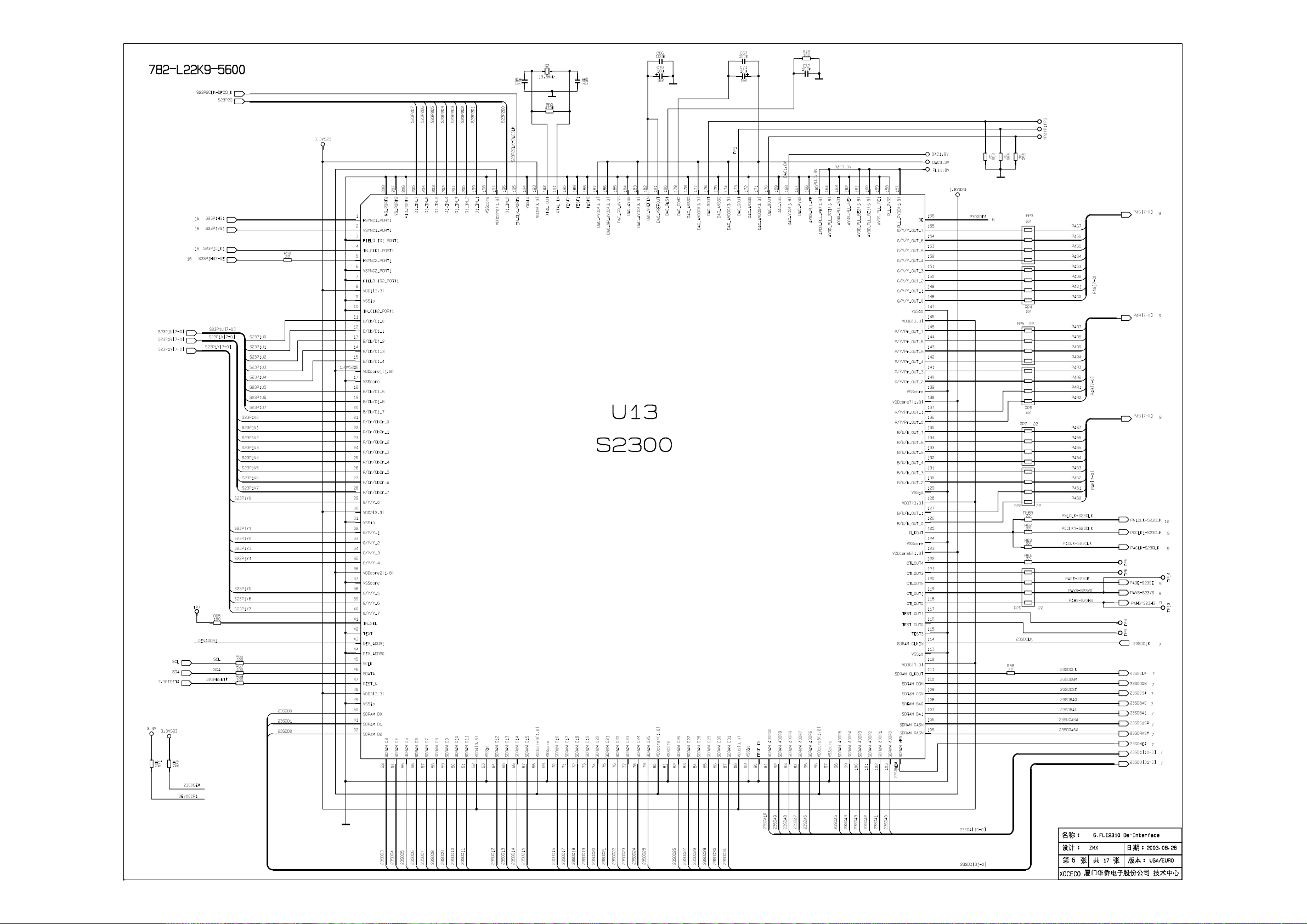
Page 15
3.Z86229
Addr B us
Row
1
CSEL
I
2
SDO
SDA
SCK
Serial
SEN
6 4 15 14 1613
SMS
VIN/
Intro
Data Line
VDD
+5V
Sliced
12
Status Reg
Control Port
Data Bus
FEW
Data CLK
Recove ry
AW
Data
Data
Slicer
Lock
Buffer
Processor
Command
Test Reg
VW
II Lock
Digital
PG
SIG
Slicer
SYNC
MUX
Address
10
4
Row
Latch
Display
6
DOT CLK
DOT CLK
DEC
ADDR
RAM
DIV
V Lock
COMP SYNC
ADDR
Decoder
RED
GREEN
Logic
Character
Generator
13
8
Latch
Display
FLD
CIR
CHAR
CW
CHAR CLK
OSCO/S
Output
4
SS CTR
Field
Line &
Control
LS
MSGR
FLD
SLS
SFLD
Control
IDrive
&MUX
BLUE
BOX
17 3 2 18
Z86229 only
CKT
POR
V/I
Ref
10
RREF
Line & Fld
Decodes
Vss(A)
11
Filter
Loop
9
LPF
Pin description:
7 PIN:Video input
2 PIN:G output
3 PIN:B output
18 PIN:R output
17 PIN:FB output
CG
Dual
Clamp
Slice Level
7
Video
8
CSYNC
CG Lines
Logic
PH1
MSYNC
FR
PH2
HIN
5
Figure 1. Z86229 Block Diagram
13
Page 16

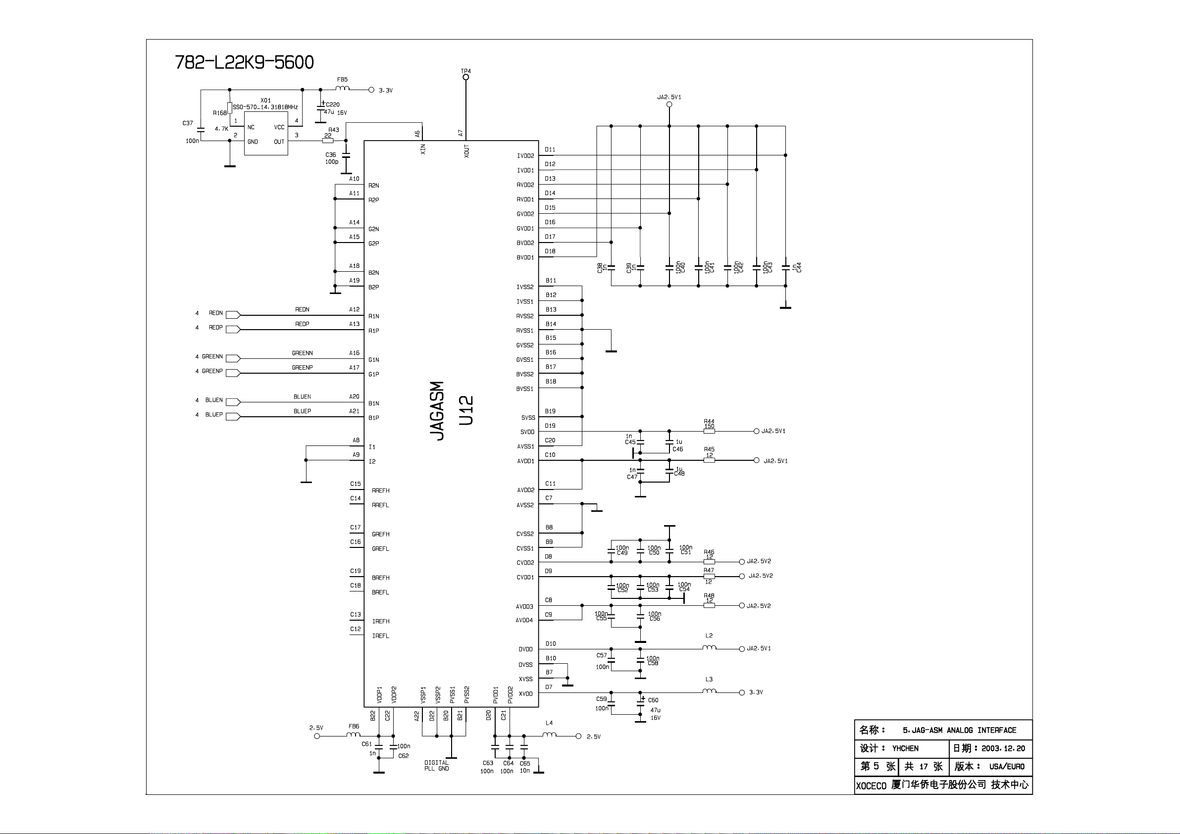
4.JAG-ASM
Panel clk
48
PIP
OVRLY
CLUT
GAMMA
OSD
OVERLAY
DITHER
ENGINE
DATA
STEER
PANEL
BE
FIFO
SYNC
SCALE
SCALE
SLOT 0
BE
FIFO
MEM
SCALE
SLOT 2
CTRL
PANEL
48
MEM
OSD
128
UNPACKER
MEM DIS
128
FIFO
64/48/32
SDRAM
48
VGA
MUX
VIDEO
PIX
VGA
DROP
VGA
FIFO
48
VGA
MUX
VIDEO
SMARTSET
SURE SYNC
SCALE
SLOT 1
PIX
VID
DROP
VID
FIFO
48
128
MEM
PACKER
MEM CAP
Memory clk
128
FIFO
Scaling clk
SDRAM INTERFACE
Figure 2. Functional Block Diagram
Vga half clk
VGA
CAPTURE
Video half clk
VID
CAPTURE
Mem clock
Panel clock
48
24
PLL 1
MICRO
INTERFACE
PLL 2
CONTROLLER
FE
24
PORT A
24
PORT B
Vga clk
Vid clk
16
PORT C
Ref clock
Micro Cont.
14
Page 17

WIRING DIAGRAM
667-L22K9-53
667-L22K9-56
Analog board
X212
IR board
55
44
X204 X201
7
10
10
7
X213
10
10
667-L22K9-09
IR
PANEL INTERFACE
P4
CONTROL
P11
AUDIO
P37
VIDEO
P32
P6 P8
P41
PCMCIA card
BACKLIGHT
P29
POWER
P2
P39
CPU board
LCD panel
335-22001-00
P40
Keyboard
667-L22K9-05 667-L40D9-90
15
Page 18

Components No.
Part Name Part No Main components and No Remark
Analog board assy’ 667-L22K9-53
CPU board assy’ 667-L22K9-56
Infra-red receive assy’ 667-L22K9-09
Push button board assy’ 667-L22K9-05
PCMCIA board assy’ 667-L40D9-90
Power supply conversion
AD-11C
Remote control set
RC-U19R-0A
Display screen
TM220WX- 71N31
302-AD11C-00
301-UL30K9-19RA
335-22001-00
N201 MSP3420G-Q (353-34200-10)
N203 M62494FP (353-62494-20)
N207 LX1722 (353-17220-30)
N205 N206 SI4532ADY
(353-45320-80)
N208 N210
U12 JAG-ASM (353-0JAG0-00)
U13 FLI2310 (353-23100-00)
U15 TFP403PZP (353-04030-10)
U29 VPC3230D (353-32300-80)
U30 MST9883B (353-98830-10)
U31 DS90C383A (353-03830-70)
U32 Z8622912SS (353-86229-10)
U2 TSC80251G2D
(353-80251-10)
U4 AT49F002NT
(352-49002-70)
Self produced
Self produced
Self produced
Self produced
Self produced
Self produced
16
Page 19

Identification criteria for the bright spot and dark spot of the LCD screen
Category criteria
One single
Bright
spo
t
Dark
spots
Total defected point ≤8 ≤7 ≤5 ≤4 /
Notes:
.1. Definition of defected point (bright spot, dark spot): It is identified as a defected point if its
2. Definition of bright spot: It is identified as a bright spot if it is bright in the state of dark field
3. Definition of dark spot: It is identified as a dark spot if it is dark in the state of white field and
spot
2 neighboring
spots
Total No. ≤5 ≤2 ≤5 ≤2 ≤3
One single
spot
Two
neighboring
spots
Total No. ≤6 ≤7 ≤5 ≤4 ≤10
area exceeds 1/2 of a single picture element (R,G,B).
and its bright size remains unchanged
its dark size remains unchanged
15" 20" 22" 30" 40" 15" 20" 22" 30" 40"
≤5 ≤2 ≤5 ≤2 ≤3
≤2 ≤1 ≤2 ≤1 ≤1
≤6 ≤7 ≤5 ≤4 ≤10
≤2 ≤2 ≤2 ≤1 ≤5
4. Definition of two neighboring points: Defects of a group of picture elements(RB,RG,GB).
Q’ty allowed Distance between two spots
≥15mm
≥15mm
≥10mm
≥5mm
17
Page 20

Trouble shooting gude
r
n
f
y
f
h
h
1. No grating
1.
Connect powe
2. yes
supply, check if the
red light is on whe
Blue
in stand-by?
No
Check the
output 13V o
Lamp off
No Yes
Yes
No Yes
No
power adapter
No
Check if the fuse of
power adapter is
blown out.
No No
Chang the
power adapter.
No
Check F1,F2
if they are
blown out?
Push key on the R/C set or push power ke
to put on the set, to check the status of
the indication lamp
No color
change
Change CPU
board
Push any key on R/C set, to
see if the indication lamp
twinkles.
Check 12th foot o
P29 is at high
voltage/?
Check 19th and ,20t
foot of P4 are at hig
electric level?
Check if F3 is blown
out?
18
Page 21

2. There is grating but no picture
t
d
h
l
t
R
n
U
U
N
r
l
U
r
Z
n
y
U
t
Check If this se
can be operate
No
No
Has
有 No
Yes
No
has
否
No
No
No
has
has
has
by R/C or pus
key?
Enter factory adjustmen
menu , execute CLEA
change
CPU
board
Calibrate CP
board again
Determine the
synchronization signa
of 65th foot of U30
EEPROM, after operatio
shut off and re-put on to
check if there is a picture?
No
Change U30
All channels
are withou
can No
pictures
Yes VGA/DVI
Screen display
O-SIGNAL
Determine the
signal of TP1,
TP2,TP3, the
should be 1VPP
Change 13
Change CP
board
Which channe
without picture?
YPrPb TV
Determine
modulate powe
supply +5V-V
Determine 1st foot of P32
if there is 1VPP signal o
noise wave?
Determine 56th foot of U29
if there is 15.734KH
line synchronizatio
signal?
Change U29
Change CP
board
Check FI on CP
board is melted
Change
TUNER 201
No
19
Page 22

3. No sound (with TV input as an example)
g
No
No No
has
has
No
Check if R282
burns.
Check if TP2 is
tri-angle wave.
Change N207
Check the output
Yes has
wave form of foot 5
and 8 of N203
Check the output wave
form foot 27,and 28
of N201
No
Check the output wave
form of foot 67 of N201
No
Check the output wave
form of foot 11 of N201
Change TUNER201
Check the solderin
problem of N207
Change N203
Change N201
4. Examples of normal trouble fixing for LC-22K9
1. Indication lamp no light: R2, false soldering, X2, joint soldering, R2,R3,LED1 no good.
2. No power supply: F2, adapter no good.
3. No grating: V8 false soldering, or no good;P29,line of X1 no good.
4. No picture: X3, adapter no good.:
5. Abnormal background color cast: P4, no good
6. Vertical or (horizontal) line interfere: Screen, no good
7. Sound no good: line of FB20,P6 or speaker, no good.
8. Earphone no good: C275 copper foil broken
9. Remote control no good: X2 joint soldering: line of R2, X2 no good.
10. Function of push key abnormal: line of X1 no good.
20
Page 23

EXPLODED VIEWS
21
Page 24

Exploded views list
22
NO. Name NO. Name
21 connector cover
20 speaker box connector
19 speaker box front cabinet
18 speaker grille
17 acryl panel
16 speaker 37 rear cabinet cover(lower)
15 light indicator 36 rotate axis cover(back)
14 speaker box rear cabinet 35 rotate axis assy'
13 main board supporter assy' 34 column
12 metallic terminal panel(left) 33 stand upper cover
11 plastic terminal panel(left) 32 stand lower cover
10 PCMCIA card slot 31 rubber cushion
9 PCMCIA board 30 rear cabinet
8 PCMCIA card door 29 speaker box socket
7 PCMCIA bracket 28 shielding cover
6 button 27 main board
5 BUTTON panel 26 metallic terminal panel(right)
4 KEY supporter 25 plastic terminal panel(right)
3 rotate axis cover(back) 24 LCD panel
2 rear cabinet cover(upper) 23 remote sensor
1 rear cabinet cover 22 connector assy'
Page 25

Page 26

Page 27

Page 28

Page 29

Page 30

Page 31

Page 32

Page 33

Page 34

Page 35

Page 36

Page 37
Page 38
Page 39

Page 40

Page 41

Page 42

Page 43

Page 44

4321
203-L30K90-03
D
VCC33EVCCL
VCC33P
2 Ground are connected atboard layout thru a thicktrace
D
R24 0 OHM
12
CB2
0.1UF
CB3
0.1UF
CB4
0.1UF
CB5
0.1UF
12
CB6
10UF
CB7
0.1UF
CB8
0.1UF
CB9
0.1UF
12
CB10
10UF
CB11
0.1UF
12
CB12
place near powerconnector
10UF
C15
100UF
C
VCC33
CB26
0.1UF
CB13
0.1UF
CB27
0.1UF
ES60x8
CB14
0.1UF
CB15
0.1UF
CB29
0.1UF
CB16
0.1UF
CB30
0.1UF
CB17
0.1UF
CB18
0.1UF
CB32
0.1UF
CB19
0.1UF
VCCA VCC
L8
FERB
CB25
0.1UF
12
CB23
100UF
12
CB20
0.1UF
12
CB22
10UF
X2
1
2
Power
C
CB34
10UF
24C01
VCC
B
CB46
VCC33
CB36
0.1UF
CB37
0.1UF
CB38
0.1UF
SDRAM
CB39
0.1UF
VCC
CB40
0.1UF
0.1UF
No need to installEZ1085 circuitry ifJ12 provide +3.3V
VCC
12
CB48
A
1 2 3 4
0.1UF
CB50
OPEN(10UF)
VCCA
CB53
0.1UF
WM8706
12
CB54
10UF
CB55
0.1UF
12
CB56
10UF
3.3V REGUALTOR
N13 2830/3.3V
3
IN
拟制
复核
标准化
工艺
批准
1
OUT
ADJ
VCC33
2
12
FRONT
B
EZ1085
CB47
100UF
型号规格
编号
ADJ
PCMCIA
INP
OUT
A
782-L40D9-9000
23
第 张 共 张
厦门华侨电子企业有限公司XOCECO
26
Page 45

87654321
203-L30K90-03D
D
V4
847
VS1#
VS2#
PC_CD1#
PC_CD2#
VCC
VCC
A[2..9]
R11
10K
R12
10K
VCC
N3A
1
2
74HCT32
N3B
4
5
74HCT32
N3C
9
10
74HCT32
C10
0.1UF
GND
N5A
2
A
3
B
1
G
74HCT139
N5B
14
A
13
B
15
G
74HCT139
VCC
C14
0.1UF
GND
2
HD[0..15] DD[0..15]
HD[0..15]
C
HA[0..2]
B
HA[0..2] DA[0..2]
HIORDY
HIOCS16#
HD0
HD1
HD2
HD3
HD4
HD5
HD6
HD7
HD8
HD9
HD10
HD11
HD12
HD13
HD14
HD15
HA0
HA1
HA2
HWR#
HWR#
HRD# DRD#
HRD#
HIORDY
HRST#
HRST#
HIRQ
HCS3#
HCS1#
LD[8..15]
VCC
HIRQ DIRQ
HCS3# DACS3#
HIOCS16# DIOCS16#
LD[8..15]
C12
0.1UF
GND
A
1 2 3 4 5 6 7 8
LCS2#
RST#
RRN1 47X4
RRN2 47X4
RRN3 47X4
RRN4 47X4
RRN5 47X4
RRN6 47X4
RRN7 47X4
LD15
LD14
LD13
LD12
LD11
LD10
LD9
LD8
LCS2#
RST#
DD0
18
DD1
27
DD2
36
DD3
45
DD4
18
DD5
27
DD6
36
DD7
45
DD8
18
DD9
27
DD10
36
DD11
45
DD12
18
DD13
27
DD14
36
DD15
45
DA0
18
DA1
27
DA2
36
45
DWR#
18
27
DIORDY
36
45
18
27
DACS1#HCS1#
36
45
N4
3
D1
4
D2
7
D3
8
D4
13
D5
14
D6
17
D7
18
D8
11
CLK
1
CLR
2
Q1
5
Q2
6
Q3
9
Q4
12
Q5
15
Q6
16
Q7
19
Q8
74F273
VCC
C11
DWR#
DACS1#
0.1UF
GND
VCC
C13
0.1UF R21 33 OHM
GND
PC_RST
PC_LOW#
PC_HI#
IO/MEM
CNTLA
CNTLB
CNTLC
CSB
VCC CB31
PC_HI#
DACS3#
PC_LOW#
DACS3#
IO/MEM
DACS3#
DRD#
DACS3#
DWR#
CNTLA
CNTLB
CNTLC
CSB
N11 1117/3.3V
IN3OUT
ADJ
1
DAC ML
DAC MC
DAC MD
WM8706 CSB
DD0
DD1
DD2
DD4
DD5
DD6 A8
DD7
WLAT
3
CE_H#
6
CE_L#
8
OE#
4
Y0
Y1
Y2
Y3
Y0
Y1
Y2
Y3
VCC
IORD#
5
6
7
WE/P#
12
IOWR#
11
10
9
12
C6
47UF
N2
3
D0
4
D1
7
D2
8
D3
13
D4
14
D5
17
D6
18
D7
1
OC
11
CLK
2
Q0
5
Q1
6
Q2
9
Q3
12
Q4
15
Q5
16
Q6
19
Q7
74HCT374
AUX2
AUX3
AUX6
AUX7
V1
FDN338P
A2
A3
A4
A5DD3
A6
A7
A9
DIRQ
R19 33 OHM
R20 33 OHM
R22 33 OHM
VCC33
PC_VCC
12
GND
R13
4.7K
C5
100UF
V2
FDN338P
12
47UF
0.1UF
C7
IO/MEM
0 = Memory Cycle, activate OE# and WE/P#
1 = I/O Cycle, activate IORD# and IOWR#
R29
4.7K
EAUX40
EAUX41
PC_VCC
GND
C8
0.1UF
R1
4.7K
VCC
VCC
VCC
R16
4.7K
PC_VCC
GND
R15
4.7K
R17
4.7K
VCC
拟制
复核
标准化
工艺
批准
C9
0.1UF
PC_VCC
VCC
VCC
R23
4.7K
R14
4.7K
R18
4.7K
DD11
DD12
DD13
DD14
DD15
CE_L#
OE#
A9
A8
WE/P#
PC_VCC
A7
A6
A5
A4
A3
A2
DA1
DA0
DD8
DD9
DD10
DIOCS16#
PHOTO_EN#
PC_CD1#
DD3
DD4
DD5
DD6
DD7
CE_H#
VS1#
IORD#
IOWR#
PC_VCC
VS2#
PC_RST
DIORDY
DACS3#
DD0
DD1
DD2
PC_CD2#
X4
1
GND1
2
D3
3
D4
4
D5
5
D6
6
D7
7
CE1
8
A10
9
OE
10
A11
11
A9
12
A8
13
A13
14
A14
15
WE/PGM
16
IREQ
17
VCC1
18
VPP1
19
A16
20
A15
21
A12
22
A7
23
A6
24
A5
25
A4
26
A3
27
A2
28
A1
29
A0
30
D0
31
D1
32
D2
33
IOIS16
34
GND
35
GND3
36
CD1
37
D11
38
D12
39
D13
40
D14
41
D15
42
CE2
43
VS1#/RFSH
44
IORD
45
IOWR
46
A17
47
A18
48
A19
49
A20
50
A21
51
VCC2
52
VPP2
53
A22
54
A23
55
A24
56
A25
57
VS2#/RFU
58
RESET
59
WAIT
60
INPACK
61
REG
62
SPKR
63
STSCHG
64
D8
65
D9
66
D10
67
CD2
68
GND4
PCMCIA
型号规格
PCMCIA
编号
782-L40D9-9000
第 张 共 张
22
厦门华侨电子企业有限公司XOCECO
26
D
C
B
A
Page 46

4321
203-L30K90-03
LD[0..7]
LD[0..7]
N9
VCC33
D
LA16
LA15
LA14
LA13
LA12
LA11
LA9
LA8
WRLL#
LA7
LA6
LA5
C
LA4
LA3
LA2
LA1
1
2
3
4
5
6
7
8
9
10
11
12
13
14
15
16
17
18
19
20
N6
A16
A15
A14
A13
A12
A11
A9
A8
W
NC
NC
NC
A18
A7
A6
A5
A4
A3
A2
A1
SST39VF080
A17
VSS
NC
A19
A10
D7
D6
D5
D4
VDD
VDD
NC
D3
D2
D1
D0
VSS
A0
40
39
38
37
36
35
34
33
32
31
30
29
28
27
26
25
24
G
23
22
E
21
LA17
LA19
LA10
LD7
LD6
LD5
LD4
LD3LA18
LD2
LD1
LD0
LOE#
LA0
8MBIT EPROM
4MBIT EPROM/FLASH
LD0
LD1
LD2
LD3
LD4
LD5
LD6
LD7
VCC
13
D0
14
D1
15
D2
17
D3
18
D4
19
D5
20
D6
21
D7
32
VCC
16
GND
OPEN 27C040/080-90
LD[0..7]
A0
A1
A2
A3
A4
A5
A6
A7
A8
A9
A10
A11
A12
A13
A14
A15
A16
A17
A18
A19
CE
OE
12
11
10
9
8
7
6
5
27
26
23
25
4
28
29
3
2
30
31
1
22
24
LA0
LA1
LA2
LA3
LA4
LA5
LA6
LA7
LA8
LA9
LA10
LA11
LA12
LA13
LA14
LA15
LA16
LA17
LA18
LA19
LA[0..19]
LCS3#
LOE#
VCCA
D
C
LCS2#
LCS3#
2-CHANNEL AUDIO OUT
WOLFSON 2-CHANNEL AUDIODAC
R54 OPEN 0
R55 0 OHM
N1
RST#
WRLL#
VCCAVCCA
4-PIN EXTENSION FOR ROM EMULATOR INTERFACE
TP1 TP3
TP4
TP2
LA20
L_OUT
LA21
R34
15k
R36
33k
R35
1k
V7
847
L
C110UF
B
VCCA
CSB
CNTLA
CNTLB
CNTLC
TWS
MCLK
A
TBCK
TSD0
R3 33 OHM
R4 33 OHM
R5 33 OHM
R6 33 OHM
R7 33 OHM
R8 33 OHM
R9 33 OHM
R10 33 OHM
ML
MC
MD
TWS-
MCLK-
TBCK-
TSD0-
8
DVDD
7
DGND
23
CSB/WO
28
MLIIS
27
MCDM1
26
MDDM0
25
MUTEB
24
MODE
1
LRCIN
5
XTI
3
BCKIN
2
DIN
AVDD
VREFP
AGND
VREFN
VOUTL
VOUTR
ZERO
VMID
15
20
14
19
C16
10uF
16
13
C17
21
18
10uF
C3
0.1UF
L_OUT
R_OUT
ZERO
12
C4
10UF
VSYNC
HSYNC
UDAC
YDAC
CDAC
VSYNC
HSYNC
Y
Cb
IR_DATA
PHOTO_EN#
R
L
UDAC
YDAC
CDAC
X1
1
2
3
4
5
6
7
8
9
10
11
12
13
14
15
VCCA
R30
15k
R32
33k
R33
1k
R28
620
R_OUTCr
拟制
复核
V6
847
R
C210UF
型号规格
编号
标准化
WM8706
PORT
工艺
第 张 共 张
21
批准
1 2 3 4
5
R37
620
PCMCIA
782-L40D9-9000
26
厦门华侨电子企业有限公司XOCECO
B
A
Page 47

87654321
203-L30K90-03D
CLK SOURCE
PLL3(pin41)
1
DCLK INPUT
0
VCC
WRLL#
WRHL#
LOE#
LA0
LA1
LA2
LA3
LA4
LA5
LA6
LA7
LA8
LA9
LA10
LA11
LA12
LA13
LA14
LA15
LA16
LA17
LA18
LA19
LD8
LD9
LD10
LD11
LD12
LD13
LD14
LD15
VD3
OPEN
(1N4148)
CRSTAL OSC
VCC
12
105
24
173
174
175
176
198
199
170
204
205
206
207
2
3
4
5
6
7
10
11
12
13
14
15
16
19
20
21
22
23
178
179
180
181
182
185
186
187
188
189
190
191
194
195
196
197
145
150
149
143
142
146
151
152
153
144
154
155
158
122
123
124
125
126
127
128
131
132
133
134
135
136
137
140
141
R43
OPEN
(10K)
EM-MARINRESET IC
VCC
N7
1
NC
2
LD[8..15]
HRST#
HRD#
HWR#
GND
3
NC
4
RES
5
VDD
V6300
27MHZ
RST#
LCS2#
LCS2#
LCS3#
LA[0..19]
LA20
LA21
LD0
LD1
LD2
LD3
LD4
LD5
LD6
LD7
LD[0..7]
LD[0..7]
LD[8..15]
HRST#
HRD#
HWR#
HIORDY
HIOCS16#
HCS1#
HCS3#
HIRQ
HD[0..15]
HD[0..15]
1 2 3 4 5 6 7 8
HA0
HA1
HA2
HCS1#
HCS3#
HIRQ
HD0
HD1
HD2
HD3
HD4
HD5
HD6
HD7
HD8
HD9
HD10
HD11
HD12
HD13
HD14
HD15
D
C
B
EAUX40
EAUX41
HA[0..2]
A
VCC
R41
4.7K
RST#
C21
OPEN
(47UF)Package: SOT-23 5L
25
28
29
30
31
CLK
RESET
LCS0
LCS1
LCS2
LCS3
LWRLL
LWRHL
LOE
LA0
LA1
LA2
LA3
LA4
LA5
LA6
LA7
LA8
LA9
LA10
LA11
LA12
LA13
LA14
LA15
LA16
LA17
LA18
LA19
LA20
LA21
LD0
LD1
LD2
LD3
LD4
LD5
LD6
LD7
LD8
LD9
LD10
LD11
LD12
LD13
LD14
LD15
HRST/EAUX3[5]
HRD/DCI_ACK/EAUX4[6]
HWR/DCI_CLK/EAUX4[5]
HRDQ/EAUX4[0]
HWRQ/DCI_REQ/EAUX4[1]
HIORDY/EAUX3[3]
HIOCS16/CAMPCLK/EAUX3[4]
HCS1FX/EAUX3[7]
HCS3FX/EAUX3[6]
HIRQ/DCI_ERR/EAUX4[7]
HA0/EAUX4[2]
HA1/EAUX4[3]
HA2/EAUX4[4]
HD0/DCI[0]/EAUX1[0]
HD1/DCI[1]/EAUX1[1]
HD2/DCI[2]/EAUX1[2]
HD3/DCI[3]/EAUX1[3]
HD4/DCI[4]/EAUX1[4]
HD5/DCI[5]/EAUX1[5]
HD6/DCI[6]/EAUX1[6]
HD7/DCI[7]/EAUX1[7]
HD8/DCI_FDS/EAUX2[0]
HD9/EAUX2[1]
HD10/EAUX2[2]
HD11/EAUX2[3]
HD12/EAUX2[4]
HD13/EAUX2[5]
HD14/EAUX2[6]
HD15/EAUX2[7]
TDMFS
TDMDR
TDMTSC
TDMDX/RSEL
NC/CAMVS
42
PLL2(pin32)
TDMCLK
ES6420
202
PLL1(pin36) PLL0(pin33)
0 114.75
0
0
0 101.25
1
1
1
1
CAMYUV0
203
0
0
1 270
1
0
0
1 94.5
1
VCC33P
L6
FERB
L7
FERB
51
AVCC(PLL)
AVCC(VDAC)
AVSS(VDAC)
112
1
18
27
VC33
VC33
VC33
VC3359VC3368VC3375VC3392VC33
AVSS(PLL)52VSS
8
111
CAMYUV1
VSS
MULTI
4.25
0
reserved
1
bypass
1
3.75
0
4.5
reserved
1
3.5
0
1
4
VCC33
VCC33VCC33E
99
104
130
148
VC33
VC33
VC33
VSS
VSS
VSS
VSS
VSS
17
26
34
43
60
67
157
76
159
VC33
VSS
84
164
VC33
VSS
91
VC33
VSS
Frequency
NA
121.5
NA
108
183
193
VC33
VSS
98
103
201
VC33
VSS
120
VC33
VSS
129
R27
1.2/1W
VSS
138
VSS
9
35
VC25
VSS
VSS
147
156
163
VCC33
R45
4.7K
VCCL
83
121
139
172
44
VC25
VC25
VC25
VC25
VC25
VC25
PCLKQSCN/CAMYUV5/AUX3[2]
HSSCN/CAMYUV7/EAUX3[0]
VSSCN/CAMYUV6/EAUX3[1]
VSS
VSS
VSS
VSS
VSS
VSS
171
177
184
192
200
208
VCC33
R38
OPEN
(4.7K)
R46
4.7K
N8
ES60x8
TWS/SEL_PLL2
TSD0/SEL_PLL0
TSD1/SEL_PLL1
SPDIF/SEL_PLL3
PCLK2XSCN/CAMYUV4
YUV0/CAMYUV2
YUV1/VREF
YUV2/CDAC
YUV3/COMP
YUV4/RSET
YUV5/YDAC
YUV6/VDAC
YUV7CAMYUV3
DBANK0/DRAS1
DBANK1/DRAS2
DSCK/DOE
DMA10
DMA11
NC/APLL
VSS
48
C36
150P
(150PF)
R39
OPEN
(4.7K)
R47
4.7K
MCLK
TBCK
TSD2
TSD3
RBCK
RWS
RSD
DCS0
DCS1
DRAS0
DCAS
DWE
DQM
DSCK
DMA0
DMA1
DMA2
DMA3
DMA4
DMA5
DMA6
DMA7
DMA8
DMA9
DB0
DB1
DB2
DB3
DB4
DB5
DB6
DB7
DB8
DB9
DB10
DB11
DB12
DB13
DB14
DB15
AUX0
AUX1
AUX2
AUX3
AUX4
AUX5
AUX6
AUX7
XIN
XOUT
33 OHM
VCC33
R40
OPEN
(4.7K)
39
40
32
33
36
37
38
47
46
45
41
PCLK2X
116
PCLK
117
EAUX30
119
EAUX31
118
106
107
108
109
110
113
114
115
100
97
72
73
74
69
71
70
101
102
DMA0
53
DMA1
54
DMA2
55
DMA3
56
DMA4
57
DMA5
58
DMA6
61
DMA7
62
DMA8
63
DMA9
64
DMA10
65
DMA11
66
DB0
77
DB1
78
DB2
79
DB3
80
DB4
81
DB5
82
DB6
85
DB7
86
DB8
87
DB9
88
DB10
89
DB11
90
DB12
93
DB13
94
DB14
95
DB15
96
R71 33 OHM
160
R72 33 OHM
161
R73 33 OHM
162
165
AUX4
166
167
168
169
49
XOUT
50
R81
27MHZ
R48
4.7K
R56 33 OHM
R57 33 OHM
YUV0
YUV1/VREF
YUV2
YUV3
YUV4
YUV5
R65 33 OHM
R66 33 OHM
XIN
R77
100K
G1
12
27M
C33
27PF
ES6420F/FP
VDAC
YDAC Y
CDAC
UDAC
VCCV
CVBS&S-VIDEO
L1
FERB
R31 0 OHM
R49 33 OHM
HSYNC
VSYNC
TP5
RN1 33x4
1 8
2 7
3 6
4 5
RN2 12x4
1 8
2 7
3 6
4 5
RN312x4
1 8
2 7
3 6
4 5
RN412x4
1 8
2 7
3 6
4 5
VCC
VCC
R69
R70
4K7
4K7
AUX2
AUX3
AUX6
AUX7
L4
3.3UH
C34
C35
27PF
1000PF
CVBS&YUV
CV
C
VCC
C24
15P
(15PF)
HSYNC
VSYNC
C31 0.1UF
VREF
R59 270
R63 33 OHM
R67 68 OHM
MA0
MA1
MA2
MA3
MA4
MA5
MA6
MA7
MA8
MA9
MA10
MA11
VCC
8
7
6
5
VCC
N3D
11
74HCT32
RGB
CV
G
Y
PB R
B
PR
C25
22P
(22PF)
TWS
TSD0
VCC33E
C32
15PF
DB[0..15]
SERIAL EEPROM
N12
S0
VCC
S1
WC
S2
SCL
GND
SDA
24C01A
R76
4.7K
13
12
MCLK
TBCK
C28
0.1UF
CS0#
RAS0#
CAS#
WE#
BANK0
BANK1
1
2
3
4
ESS REMOTE INTERFACE
R78 33 OHM
R42
75 OHM
R50
75 OHM
R58
75 OHM
MA0
MA1
MA2
MA3
MA4
MA5
MA6
MA7
MA8
MA9
MA10
MA11
CKE
DQMX
IR_DATA
L2 2.7UH
C19
470PF
L3 2.7UH
C22
470PF
L5 2.7UH
C29
470PF
N10
23
A0
24
A1
25
A2
26
A3
29
A4
30
A5
31
A6
32
A7
33
A8
34
A9
22
A10
35
A11
38
CLK
37
CKE
19
CS
18
RAS
17
CAS
16
WE
15
DQML
39
DQMH
20
BA0
21
BA1
36
NC
40
NC
4Mx16 SDRAM (9ns)
32/64MBIT SDRAM
拟制
复核
标准化
工艺
批准
C20
470PF
C23
470PF
C30
470PF
DQ0
DQ1
DQ2
DQ3
DQ4
DQ5
DQ6
DQ7
DQ8
DQ9
DQ10
DQ11
DQ12
DQ13
DQ14
DQ15
VCC
VCC
VCC
VCCQ
VCCQ
VCCQ
VCCQ
VSSQ
VSSQ
VSSQ
VSSQ
VSS
VSS
VSS
5
VDAC
YDAC
CDAC
UDAC
VCCV
VD4
1N6263
2 1
VD7
1N6263
2 1
VCCV
VD10
1N6263
2 1
VD12
1N6263
2 1
VCC33
DB0
2
DB1
4
DB2
5
DB3
7
DB4
8
DB5
10
DB6
11
DB7
13
DB8
42
DB9
44
DB10
45
DB11
47
DB12
48
DB13
50
DB14
51
DB15
53
1
14
27
3
9
43
49
6
12
46
52
28
41
54
型号规格
编号
第 张 共 张
20
VDAC
YDAC
VIDEO OUT
CDAC
UDAC
VCCV
VD5
1N6263
2 1
VD8
1N6263
2 1
CRITICAL TRACES
MOST
LEAST
CLOCKS
ADDRESS
CAS
WE
RAS
CSx
DQM
PCMCIA
782-L40D9-9000
厦门华侨电子企业有限公司XOCECO
26
D
C
B
A
 Loading...