

Page 1
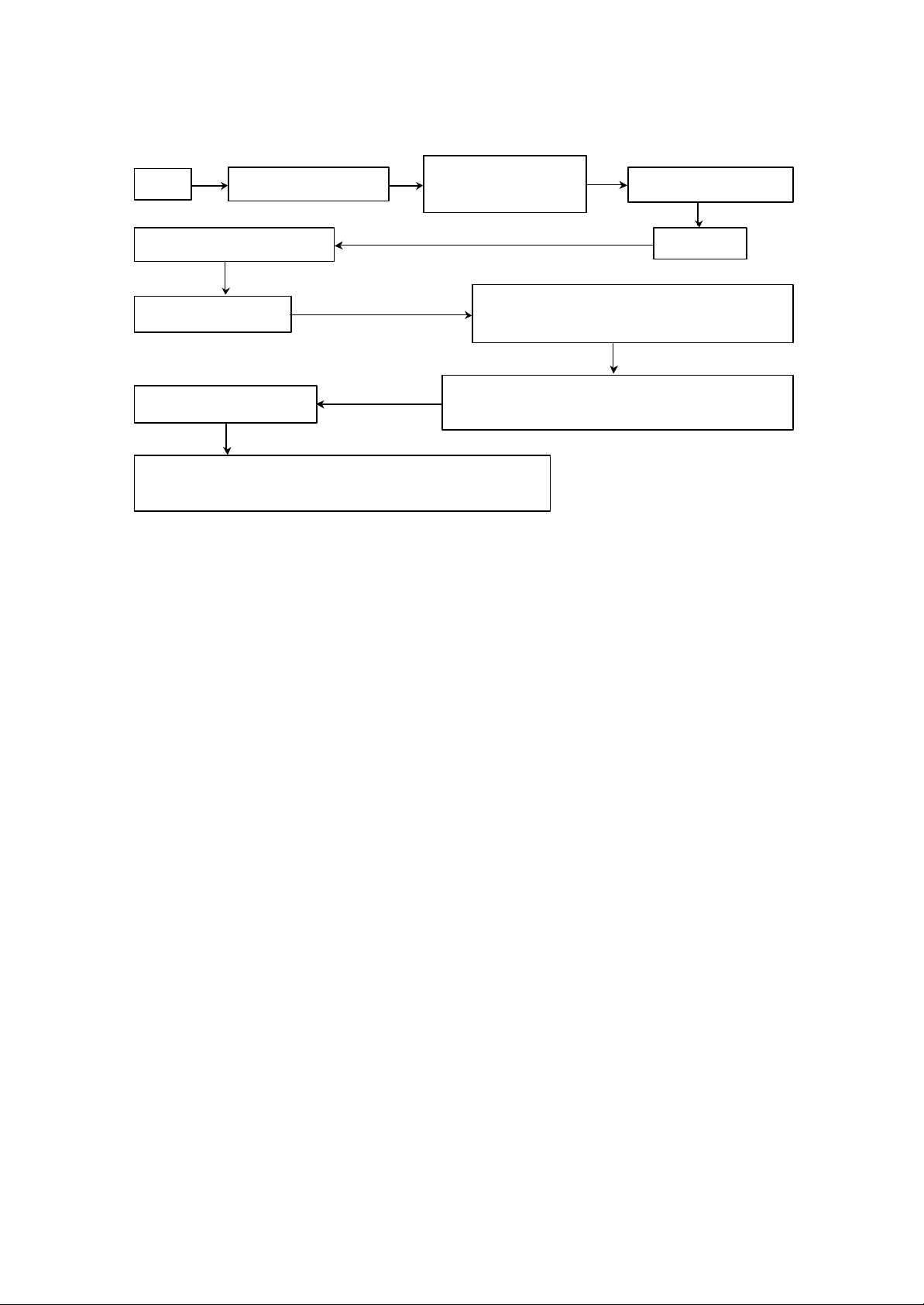
THE ALIGNMENT FLOW CHART
PIF
To fit the front cabinet,
Focus
alignment, focus, high
BTSC, secret code setting, AV function check.
Control buttons, channels, white balance, sound, hit the set
with
Factory items’ adjustment
Heatrun for 2 hours
To fit the back cabinet
B+, AGC,H-frequency
external degaussing
Preheat for 30 minutes
White balance revoltage,
X-ray protection test, sound power test, CCD, V-chip,
INSTALLATION AND SERVICE ADJUSTMENTS
GENERAL
In the majority of cases, a color television receiver will need only slight touch-up adjustment upon
installation. Check the basic characteristics such as FS、EHV and focus. Observe the picture for
good black and white details without objectionable color shading. If color shading is evident,
demagnetize the receiver.
If color shading still persists, perform purity and c onvergence adjustments. This should be all that is
necessary to achieve optimum receiver performance.
FOCUS ADJUSTMENT
Adjust the FOCUS control (on T471) for well defined scanning lines on the picture screen.
HIGH VOLTAGE CHECK
CAUTION: These is no HIGH VOLTAGE ADJUSTMENT on this chassis. Checking should be
done following the steps below.
1. Connect an accurate high voltage meter to the second anode of the picture tube.
2. Turn on the receiver. Set the BRIGHTNESS and CONTRAST controls to minimum (zero beam
current).
3. High voltage will be measured below 24kV.
4. Vary the BRIGHTNESS control to both extremes to be sure the high voltage does not exceed the
limit under any conditions.
FS CIRCUIT CHECK
The Fail Safe (FS) circuit check is indispensable for the final check in the servicing. Checking
should be done following the steps below.
- 3 -
Page 2
1. Turn the power switch on and adjust customer controls for normal operation.
Check that the set returns to normal operation when pin
34 of N101 on the Main Board is grounded with jumper
Power Circuit or Horizontal Circuit
Check if the voltage across capacitor
C411 is approximately 21V.
2. Temporarily short R412 on the Main Board with a jumper wire. Raster and sound will
disappear.
3. The receiver must remain in this state even after removing the jumper wire. This is the evidence
that the FS circuit is functioning properly.
4. To obtain a picture again, temporarily turn the receiver off and allow the FS circuit more than 30
seconds to reset. Then turn the power switch on to produce a normal picture.
Troubleshooting Guide for Fail Safe Circuit
YES NO
NO
YES
Faulty
Defective Fail Safe Circuit
PIF alignment
1) Apply DC 12V to output pin of N551(pin3 of N551 ) , connect pin7 of LA76814(N101)
to GND.
2) Apply 95dBμ, 45.75MHz RF signal to the tuner's IF pin through a 1000P ceramic
capacitor. Connect the DC voltameter's⊕pole to LA76814 pin 47 , ⊙ pole to GND.
Note: For LA76814 ES01 version, the voltameter's⊕pole should connect to pin50 .
3) Adjust T202 with a non-inductive screwdriver until the reading on the DC voltameter is DC
3.6V±0.01V.
B+ CHECK
1) Prepare the test equipment.
2) Use the DC voltameter at DC 200V position to test VD551⊕, i.e. B+.
3) Connect the power plug to AC 120V/60Hz, turn on the power switch, wait for normal raster,
then adjust RP551 to make B+ = 110V±0.5V.
Test point
VD551⊕ VD556⊕ VD554⊕ VD555⊕
DC(V) 110 25 15 18
- 4 -
Page 3

TEST MODE SET(CHECK)
TEST MODE ADJUSTMENT INSTRUCTION
TEST MODE adjustment is a special adjustment which is controlled by I2C BUS. The TV set has
been set at optimum mode at the factory. Except for special need, such as replacing CRT
MEMORY IC etc., it is hoped not to adjust it.
CIRCUIT DIAGRAM OF TEST MODE ADJUSTMENT
VCC
N1
LC7461M-8103
1 C3 24
2 C2 23
3 C1 22
VCC 4 C0 21
5 C4 20
6 C5 19
7 18
VCC 8 17
9 16
10 15
11 14
G1 12 13
C1 C2
C3 VD1
R1
V1
R2
PIN20
PIN15
PIN14
PIN1 PIN4 PIN2 PIN3
1
.
MENU
VOL-
3
RECALL NC PIN17
TC/AV
VCHIP IFC GEO PICTURE
PTRN DP FACT W/B PIN13
4 2
8 6 7 5 PIN19
NC 10/0 NC 9 PIN18
CH+ PROD POWER VOL+ PIN16
CH- SCAN MUTE
Page 4
1. N1 LC7461M-8103 2. VD1 IR-LED
3. V1 2SC1815 4. R1 RT14-1/4W-1Ω-J
5. R2 RT14-1/4W-220Ω-J 6. C1 C2 CT1-05B-2B4-63V-220PF-K
7. C3 CD110X-6.3V-100UF-M 8. G1 455KHZ 9.VCC
H-center adjustment, V-amplitude, linearity, S-correction, V-center adjustment
1) Press the GEO button on the remote controller to enter into the ADJUST mode.
2) Select the H.PHASE item, adjust the level to make the left and right picture sysmmetrical.
3) Select the V.POS item , adjust the value to make V-center and the CRT's geometric center is in
accordance. Then select the V.SIZE item, adjust the value to make the overscan is less than or
Equate 10% .
4) Select the V.LINE item, adjust the value to make the upper and lower grid's(on the screen)
vertical distance equal. Select the V.SC item, adjustthe value to make the vertical distance from
upper grid to middle screen is equal to the vertical distance from lower grid to middle screen.
5) Press the PICTURE button on the remote controller to save the data.
White balance
1) Press the W/B button on the remote controller to enter into the ADJUST mode.
2) Set the value of item as the following table:
Name Function Default Value
R-BIA Red Bias 95 0~255
G-BIA GreenBias 127 0~255
B-BIA BlueBias 95 0~255
R-DRV Red Drive 48 0~127
G-DRV GreenDrive 7 0~15
B-DRV BlueDrive 48 0~127
3) Press the DP button , Select the Subbrishtness item ,Set the value of Subbrishtness =85, then
press "SCAN" button. Adjust the SCREEN potentiameter clockwise until a slight bright
horizontal line appears on the screen. Adjust the value of R-BIA, G-BIA and B-BIA, until the
line change white. Press " SCAN " button again. Then decrease S-BRI to a proper value.
Name of button 1 3 5 7
Function Red Drive + Green Drive + Blue Drive + Subbrishtness +
Name of button 2 4 6 8
Function Red Drive - Green Drive - Blue Drive - Subbrishtness -
4) Press the W/B button,Then press the PICTURE button on the remote controller to save the
data.
, sub-brightness adjustment
Page 5

ADJUST MENU LIST
Press the PROD button on the remote controller to enter into the ADJUST mode.
Item Name Function Default Value
1 FISYS Filter System 0 0-3
2 HFREQ H freq 28 0-63
3 TRTES Trap Test 0 0-7
4 GMODE Gray Mode 0 0-1
5 V LIN V Line 12 0-31
6 RGDEF R/G Gamma Defeat 5 0-1
7 BGSLC B Gamma Select 0 0-3
8 AFG&G AFC Gain & gate 1 0-1
9 OSCNT OSD Contrast Control 2 0-3
10 CBYPS Chrome Bypass 0 0-1
11 CRB/W Cross B/W 0 0-3
12 HBLKL H BLK L 6 0- 7
13 HBLKR H BLK R 4 1- 7
14 BSHLD Bright ABL Threshold 7 0-7
15 EMABL Emeragence ABL Defeat 0 0-1
16 MDSTP Bright Mid Stop Defeat 0 0-1
17 FMLBL FM Level 2 0-31
18 FBPSW FBP BLK SW 0 0-1
19 DIOSD Dingital OSD 0 0-1
20 BRABL Bright ABL Defeat 0 0-1
21 VDLBL Video Level 7 0-7
22 VERSC Vertical S-correction 5 0-31
23 COREW Coring Enable 1 0-1
24 VISYS VIF.SYS.SW 0 0-1
Page 6

USA CHANNEL FREQUENCY TABLE (181 CH)
P IF=45.75 MHz
C IF=42.17MHz
S IF=41.25MHz
UNIT: MHz
BAND
VHF
Low
VHF
High
P
CHANNEL
A-6 85.25 89.75 131 W+16 391.25 395.75 437
A-5 91.25 95.75 137 W+17 397.25 401.75 443
A-4 97.25 101.75 143 W+18 403.25 407.75 449
A-3 103.25 107.75 149 W+19 409.25 413.75 455
A-2 109.25 113.75 155 W+20 415.25 419.75 461
A-1 115.25 119.75 161 W+21 421.25 425.75 467
10 193.25 197.75 239 18 495.25 499.75 541
11 199.25 203.75 245 19 501.25 505.75 547
12 205.25 209.75 251 20 507.25 511.75 553
13 211.25 215.75 257 21 513.25 517.75 559
W+1 301.25 305.75 347 36 603.25 607.75 649
W+2 307.25 311.75 353 37 609.25 613.75 655
W+3 313.25 317.75 359 38 615.25 619.75 661
W+4 319.25 323.75 365 39 621.25 625.75 667
W+5 325.25 329.75 371 40 627.25 631.75 673
W+6 331.25 335.75 377 41 633.25 637.75 679
W+7 337.25 341.75 383 42 639.25 643.75 685
W+8 343.25 347.75 389 43 645.25 649.75 691
W+9 349.25 353.75 395 44 651.25 655.75 697
W+10 355.25 359.75 401
CARRIER
2 55.25 59.75 101 W+11 361.25 365.75 407
3 61.25 65.75 107 W+12 367.25 371.75 413
4 67.25 71.75 113 W+13 373.25 377.75 419
5 77.25 81.75 123 W+14 379.25 383.75 425
6 83.25 87.75 129 W+15 385.25 389.75 431
A 121.25 125.75 167 W+22 427.25 431.75 473
B 127.25 131.75 173 W+23 433.25 437.75 479
C 133.25 137.75 179 W+24 439.25 443.75 485
D 139.25 143.75 185 W+25 445.25 449.75 491
E 145.25 149.75 191 W+26 451.25 455.75 497
F 151.25 155.75 197 W+27 457.25 461.75 503
G 157.25 161.75 203 W+28 463.25 467.75 509
H 163.25 167.75 209 W+29 469.25 473.75 515
I 169.25 173.75 215 14 471.25 475.75 517
7 175.25 179.75 221 15 477.25 481.75 523
8 181.25 185.75 227 16 483.25 487.75 529
9 187.25 191.75 233 17 489.25 493.75 535
J 217.25 221.75 263 22 519.25 523.75 565
K 223.25 227.75 269 23 525.25 529.75 571
L 229.25 233.75 275 24 531.25 535.75 577
M 235.25 239.75 281 25 537.25 541.75 583
N 241.25 245.75 287 26 543.25 547.75 589
O 247.25 251.75 293 27 549.25 553.75 595
P 253.25 257.75 299 28 555.25 559.75 601
Q 259.25 263.75 305 29 561.25 565.75 607
R 265.25 269.75 311 30 567.25 571.75 613
S 271.25 275.75 317 31 573.25 577.75 619
T 277.25 281.75 323 32 579.25 583.75 625
U 283.25 287.75 329 33 585.25 589.75 631
V 289.25 293.75 335 34 591.25 595.75 637
W 295.25 299.75 341 35 597.25 601.75 643
S
CARRIER
LOCAL BAND CHANNEL P
CARRIER
UHF
45 657.25 661.75 703
S
CARRIER
LOCAL
- - 11
Page 7

USA CHANNEL FREQUENCY TABLE (181 CH)
P IF=45.75 MHz
C IF=42.17MHz
S IF=41.25MHz
UNIT: MHz
BAND CHANNEL P CARRIER S CARRIER LOCAL
UHF
46 663.25 667.75 709
47 669.25 673.75 715
48 675.25 679.75 721
49 681.25 685.75 727
50 687.25 691.75 733
51 693.25 697.75 739
52 699.25 703.75 745
53 705.25 709.75 751
54 711.25 715.75 757
55 717.25 721.75 763
56 723.25 727.75 769
57 729.25 733.75 775
58 735.25 739.75 781
59 741.25 745.75 787
60 747.25 751.75 793
61 753.25 757.75 799
62 759.25 763.75 805
63 765.25 769.75 811
64 771.25 775.75 817
65 777.25 781.75 823
66 783.25 787.75 829
67 789.25 793.75 835
68 795.25 799.75 841
69 801.25 805.75 847
- - 12
Page 8

Page 9

VIDEO
IN
VIDEO
OUT
IR TX
LC7461M-8103
IR RX
LOC
B
CPU N701
LC863240A-5V11
MEMORY
N702
AT24C04
K
A101
TUNER
SAWF
D
GRAM
A
I
Z201
AUDIO
IN
AUDIO
OUT
AMP
LA4225A
AUDIO
12V
IN OUT IN OUT
VIDEO
FM
5V
18V
CHROMA
B
DRIVER
G
CRT
R
SIF
VIDEO
V432
2SD1651
H OUT
PIF
N101
DEFLECTION
LA76814
V OUT
N451
LA7840
2SC4423
AC 120V
POWER
V513
110V
CRT
FBT
T471
Page 10

LA76814ICBLOCKDIAGRAM
AudioOutput
FMOutput
PIFAGCFilter
RFAGCOutput
PIFInput1
PIFInput2
IFGround
IFVcc
FMFilter
AFTOutput
BusData
BusClock
ABL
2.5
2.5
2.53
2.56
2.8
2.8
5V
2.12
2.34
4.8
4.8
3.52
3
SIFInput
2.4
SIFAPCFilter
1.93
SIFOutput
2.11
Ext.AudioInput.
2.3
FLLFilter
4
VCOCoil1
4
VCOCoil2
3.7
APCfilter
2.18
VideoOutput
2.53
BlackLevelDetector
2.7
InternalVideoInput(S_CIN)
Video/VerticalGround
5V
2.4
ExternalVideoInput(YIN)
RedInput
GreenInput
BlueInput
FastBlankingInput
RGBVcc
RedOutput
GreenOutput
BlueOutput
B.AKBInput
Vertical
Output
RAMPALC
Filter
Holizontal/Bus
HolizontalAFC
Holizontal
Vcc
Filter
Output
1.1
1.15
1.13
0
8
3.16
3.16
3.05
0
2.51
2.63
5V
2.63
0.48
Video/Vertical/BUSGround
0
2.32
SelectedVideoOutput
3.06
ACCFilter
2.64
3.58MHzCrystal
0.53
fsc(3.58MHz)Output
3.3
ChromaAPC1Filter
0.35
KillerFilter
0
X-RAY
HolizontalGround
0
2.9
OSDContrast
NC
NC
1.7
VCOIREF
1.11
FBPInput
Page 11

EW0130KB
U902
OMIT-SS-112LM
RL551
VD553
D
5V
T3.15A125V
400KM2200p
B7
QHXC-54F
AC110V
60HZ
1/2DJ220K
F501
R501
LIVE AREA
DJ22K
R515
C515
FJ0.01
C533
1/2CK5.6M
R531
B5
5V
10V470
C570
AN7805
3
+
N553
2
1
AN7812
12V
B6
3
N552
2
1
2SC1815
VD402
VD401
D
D
+
C408
50V1
330K
R403
R404
820
R408
2.2K
AN7805
1
2
3
L909
250HM0.1
C501
2SC3807
V512
+
25V1000
C565
17V
N551
V552
100
B2
JLB1606
L501
R517
R562
2FJ1
R561
10K
50V1
3.3K
2SA1015
D
2.2K
2
2
13
ES1
C407
R402
V511
VD516
R526
VD555
1.2K
+
250HM0.1
R567
FK0.068
27
H OUT
C502
5.6K
14
+
25V1000
C564
10K
C406
H AFC FIL
C532
400KM470p
R511
ES1
15
R519
VD554
EU2Z
R566
2SB892
V554
1/2DJ270
R400
+
16V220
C404
C405
0.01
26
VD517
FK0.1
1KV4700p
C520
12
1KV470p
1FJ2.2
FK0.22
C402
FK0.47
25
VCC (H)
7WK1
R502
C514
2SC4423
V513
1
1
11
C554
B1-ADJ
R569
B-2K
R553
4.7K
HZ6C3
VD561
VD552
D
50V0.47
C401
C403
R401
2.2K
24
RAMP ALC.FIL
D
2SJ27
+
V OUT
0
VD514
15K
R524
Z2073
RP551
23
00
0
PTDCA1BF3R0Q100
JLB1606
L502
200V470
C507
R522
L504
7
7
8
2KV470p
C551
+
1/2DJ100K
R552
V553
2SC1815
R554
150K
110V
R244
2.7K
22
AKB IN
1
2
2
1
TJC2-2A
00
RT501
+
1/2SJ100K
R520
1KV4700p
C516
R525
2SJ6.8
9
RU3A
VD551
C561
160V220
R551
2SJ47K
OMIT-SS-112LM
RL552
B1
21
B OUT
XS501
1000KM1000p
C504
1000KM1000p
C506
500K1000p
BCK-40-5B
3
3
10
R555
1/2DJ47K
20
G OUT
C518
22K
R OUT
RM11C
RM11C
T511
16V47
0.01
19
R556
+
VD504
VD506
PC817B
C244
C245
VCC (RGB)
N501
18
RM11C
VD503
RM11C
VD505
12
34
R243
270
17
1000KM1000p
C503
1000KM1000p
C505
B5
5V
R722
1.5K
VD703
HZ4A2
R723
8.2K
2SC 1815
R733
10K
10K
R732
47K
100
ABL13R IN14G IN15B IN16BLANK IN
R242
V705
R730
100
12
V704
2SC1815
R729
150K
LC863248A
R241
DATA11CLOCK
10K
N701
100K
0.01
R721
4.7K
R736
R114
C118
AFT OUT
2SC1815
470
V703
10K
10K
21
H SYNC
R OUT22G OUT
R738
4.7K
100K
C117
50V1
+
10
FM FIL
R728
R734
R731
20
V SYNC
23
4.7K
R113
9
16V2.2
50V1
19
B OUT
24
R740
3.3K
3.3K
L102
15UH
+
16V100
C115
C116
0.01
8
VCC (VIF)
C714
+
C713
+
R742
R743
5V
GND(IF)
0.01
FILT18CVBS-IN
BLANK
25
B7
7
R724
4.7K
V702
2SA1015
SCL
SDA
AGC
VOLUME-R
MUTE
R758
B5
5V
22K
6
37
2.2K
16V2.2
R102
100K
R752
VOLUME-L
AV238AV1
R759
+
C103
22K
5
22K
FK0.022
1K
R750
WOOF-VOL
R760
C611
NC
R103
10K
4
39
22K
D
16V100
R735
R761
VD601
+
C603
3.3K
3
ALARM
AV/TV
40
10K
R611
R748
22K
R762
22K
R601
2SA1015
V601
R105
100
B5
5V
22K
2
50/60
BAND241BAND1
22K
2SC1815
C729
270K
330
R726
R725
38M
VIF IN2
RESET
I
220
6
R720
10K
R707
680
L701
39UH
R708
10K
+
16V47
C701
C704
15P
C705
13
SCL1
30
16V47
0.01
0.01
2
C702
0.01
R753
22K
+
C719
C720
1K
C122
AUDIO OUT
VDD12KEY IN
SAFTY
82
1
390K
31
10K
R109
R111
R709
11
XTAL2
S-VHS
32
R754
22K
0.01
LA76814K
N101
18P
32K
R755
2SC2216
C112
G701
10
SD
33
22K
V102
R756
7VT8
POWER
GND9XTAL1
WOOFER ON/OFF
SIF
IR
36
34
35
R766
R757
100
22K
22K
C110
0.01
R108
5.6K
C111
0.01
R110
220
R107
100
12V
B6
+
C601
16V10
C703
0.01
14
15NC16
17
AFT IN
AGC IN
SDA0
SDA1
SCL0
27
29
28
26
R747
R751
R749
22K
22K
22K
1
4
2 3
AT24C04
N702
GND
VCC
SDA
SCL
R745
7
8
5
6
R744
220
Q45.75H1
Z101
R119
1K
FK0.022
FK0.022
C120
C121
C119
0.01
3
4
5
VIF IN1
RF AGC
PIF AGC
FM OUT
16V100
C101
+
0.01
5V
R104
100
R746
1
SURROUND
42
R763
22K
12V
B6
R602
10K
V602
5V
C102
22K
R765
R764
110V
B1
B7
2SJ10K
R718
UPC574
N706
50V4.7
C708
+
33V
5V
R101
33K
TDQ-3B8/136F
A101
IF
B5
5V
SCN-4Y
150K
27K
8.2K
4.7K
3.9K
2.7K
1.5K
XS1702
R1701
R1702
R1703
R1704
R1705
R1706
R1707
CH+
CH-
V+
V-
MENU
TV/AV
SC01
SC02
SC03
SC04
SC05
SC06
R1735
470
VD1701
BT204L-31
HS0038
N1703
XP1807
R1803
AUDIO
L814
VIDEO OUT
TEM2028K
XS1805
TEM2028K
TEM2028K
L1802
VIDEO
TEM2028K
L813
AUDIO IN
XS801-1
L1801
TEM2028K
L812
VIDEO IN
XS1803
L811
CIRCUIT DIAGRAM OF MODEL H2020
XS1811
16V100
C604
+
4.7K
2SC1815
V603
R604
SCN3-2Y
SCN3-2Y
XP601
XP601
47K
XP902
SCN-5Y
TEM2028K
AUDIO OUT
R409
680
2SC2383-O
V431
R433
1/2SJ1K
C433
500KK3900p
500KK1000p
C432
ABL
YC0008
L432
39n400V
C437
110V
B1
R471
5W1.8
TEST
TP-G
R232
10K
TP-H
TEST
R233
1/2DJ1.5K
C231
50NP1
WARNING:
(1) D: 1S1555; 1N4148; 1S2473; 1S2076; D5442;
(2) 0.01:CT1-08B-2F4-63V-0.01uF-Z;
(3) KK470: CT1-06B-2B4-63V-470uF-K
(4) FKXXX: CL11-63V-XXXuF-K
(5) 200NJXXX: CBB22-200V-XXXuF-J
(6) 1500MJXXX: CBB12-1600V-XXXpF-J
VCO IREF
FBP IN
28
4.7K-J
R273
R413
10K
4.7K
JDT1904
YC0008
L431
1500MJ10000p
C435
2
1FJ1
EU01
+
250V22
C474
29
0.01
3K
R274
T431
35V100
C472
EU01
1FJ1
R474
VD474
C279
R272
+
VD472
1
1
CLOCK OUT
30
+
160V47
C434
2SD1651
V432
B4
24V
R472
10
10
SCREEN8HV
VCC (CCD)
31
+
C276
16V10
R274
4.7K
2W220
R434
FO
OSD CONTRAST
GND (CCD/H)
33
32
C412
50V1
R414
10K
R275
R415
3K
3.9K
25V47
C411
+
VD411
EU01
B1
24V
220K
H-PULSE
9
4
9
4
T471 T
1FJ0.22
R491
180V
B3
R612
16V10
470
C612
+
R802
1
2
3
4
25V1000
C613
+
5
R803
56K
16V10
C801
+
R811
75
R809
100K
R922
100
C923
CJ390p
V922
2SC2688
680
R928
1/2SJ2.7K
2SJ10K
R927
0.01
C205
16V470
C206
VD451
R452
1
100FK0.1
C459
XS402
VCC (V/C/D)
43
C204
50V1
+
35V100
C451
+
INT VIDEO IN
44
+
16V4.7
C203
500FK10p
C455
BLK STRETCH FIL
VIDEO OUT
45
46
R201
1K
+
50V0.47
C137
+
R202
1.2K
7
6
5
4
3
2
GND
1
APC FIL
47
PUMP OUT
VCC2
INPUT
VCC1
OUTPUT
VCO COIL48VCO COIL
49
470p
ST6017
T101
R822
1K
R821
4.7K
R806
68K
R807
220
V801
2SC1815
LA7840
N451
NON INPUT
C140
16V10
+
VCO FIL
50
50V0.47
+
390
V821
2SC1815
C803
K6D
EXT AUDIO IN
51
330
C139
R127
18p
R805
27K
SCN-4Y
XP901
1
1
2
2
3
3
4
4
FO
SIF OUT
R122
C125
+
16V10
16V470
50V0.47
C934
+
VD933
D
52
50V1
C931
C933
1000p
C123
R121
1K
+
C821
12V
+
2KV1000p
SIF APC FIL
53
FK0.01
C124
+
15UH
B6
R935
39
C939
5
5
7
7
1
1
SIF IN
54
39p
L121
16V470
C804
+
12V
B6
54321
2SC1815
V932
R940
33
10
10
9
9
A51JUL91X91
U901
C126
SCN-5
XP902
SCN-5Y
DJ10K
8
8
XS403
R900
16V10
C802
+
100
R810
75
R933
1.5K
16V10
11
11
W902 JG0034
R932
15K
C932
+
K9N
TJC2-1A
XS901
GZS8-6-4F
R931
1K
2SA1015
V931
82
CJ390p
C921
680
R804
R926
R924
330
56p
VD921
D
SEL VIDEO OUT
EXT VIDEO IN
3K
R458
12K
R454
R453
12K
APC1 FIL
39
16V0.47
+
5.6K
C453
1000p
R455
+
C456
50V4.7
+
25V1000
C457
TJC2-5Y
XP402
R451
C210
39K
1
1
40
50V1
R456
12K
R457
2
2
GND (V/C/B)
41
24V
B4
L451
18UH
25V1000
C452
+
+
C454
VD452
1Z75
1/2DJ180
R460
100FK0.033
C458
3
3
42
EM01Z
4
4
TJC2-5A
APC2 FIL36FSC OUT
KILL FLT
X-RAY
35
34
+
HZ7C1
VD412
R412
22K
8.2K
1/2SJ3.3
R418
+
R446
160V4.7
C444
3
2
3
C274
0.01
FK0.047
C207
50V0.47
C208
R205
+
22K
200FK0.39
C441
2069
SCN-4Y
XS401
XTAL
38
37
R271
C209
1K
18P
S3.58
G201
R206
1/2SJ1K
R441
L441
16V100
C450
+
12V
B6
1SJ1
R459
1K
1/2DJ120
R461A
12V
B4
C911
LA4225A
N601
INPUT
NON INPUT
GND
OUT
VCC
16V10
C805
+
R808
1K
R914
330
56p
C913
2SC2688
R916
VD911
D
R918
1/2SJ2.7K
17V
B2
+
C616
25V1000
C617
0.01
used for components replacement pointed out by the mark.
R801
22K
C809
2200
R822
1K
TJC3-2A
XS601
SCN3-2Y
XP601
5W16OHM
5W16OHM
B901
B902
CRT BOARD
R904
330
R912
100
CJ390p
C901
V912
560
R906
2SJ10K
R917
56p
VD901
D
1/2SJ2.7K
R908
C903
100
V902
2SC2688
2SJ10K
R902
R907
NOTICE:
PART NO.:IET010806
 Loading...