Xitron 2551, 2551E User Manual

X
ITRON TECHNOLOGIES
USER'S GUIDE
2551/2551E
Single-Phase
P
ower Analyzer


Warranty 3
Warranty
The Xitron Technologies instrument is warranted against defects in material and
workmanship for a period of two years after the date of purchase. Xitron Technologies
agrees to repair or replace any assembly or component (except batteries) found to be
defective, under normal use, during the warranty period. Xitron Technologies’ obligation
under this warranty is limited solely to repairing any such instrument which in Xitron
Technologies’ sole opinion proves to be defective within the scope of the warranty, when
returned to the factory or to an authorized service center. Transportation to the factory or
service center is to be prepaid by the purchaser. Shipment should not be made without
prior authorization by Xitron Technologies.
The warranty does not apply to any products repaired or alt ered by persons not authorized
by Xitron Technologies, or not in accordance with instructions provided by Xitron
Technologies. If the instrument is defective as a result of misuse, improper repair, or
abnormal conditions or operations, repairs will be billed at cost.
Xitron Technologies assumes no responsibility for its product being used in a hazardous
or dangerous manner, either alone or in conjunction with other equipment. Special
disclaimers apply to this instrument. Xitron Technologies assumes no liability for
secondary charges or consequential damages, and, in any event, Xitron Technologies'
liability for breach of warranty under any contract or otherwise, shall not exceed the
original purchase price of the specific instrument shipped and against which a claim is
made.
Any recommendations made by Xitron Technologies or its Representatives, for use of its
products are based upon tests believed to be reliable, but Xitr on Technologies makes no
warranties of the results to be obtained. This warranty is in lieu of all other warranties,
expressed or implied, and no representative or person is authorized to represent or assume
for Xitron Technologies any liability in connection with the sale of our produc ts other
than set forth herein.
Instrument Serial Number: ___________________________ _______

4 2551 User's Guide
T
Document Part Number: MO-2551/2551E-M Revision E
Print date: January 31, 2006
Copyright
Copyright© 1998 - 2000 Xitron All rights reserved.
All rights reserved. No part of this publication may be reproduced, transmitted,
transcribed, stored in a retrieval system, or translated into any language in any form
without prior written consent from Xitron Technologies. This product manual is
copyrighted and contains proprietary information, which is subject to change without
notice. The product's displays and manual text may be used or copied only in accordance
with the terms of the license agreement.
iTRON
or registered trademarks are acknowledged as the exclusive property of their respective
owners.
In the interest of continued product development, Xitron Technologies Inc., reserves the
right to make changes in this guide and the product it describes at an y time, without
notice or obligation.
ECHNOLOGIES
is a trademark of Xitron Technologies. All other trademarks
Xitron Technologies Incorporated
9770-A Carroll Centre Rd
San Diego, California 92126
Telephone: (858) 530-8099
Fax: (858) 530-8077
E-mail: sales@xitrontech.com
E-mail: support@xitrontech.com
ISO-9001: 2000
Cert. No. A0001474-1

Contents 5
Contents
INTRODUCTION _________________________________________________ 11
Scope ________________________________________________________ 11
Features ______________________________________________________ 12
FUNCTIONAL DESCRIPTION _____________________________________ 13
Theory of Operation____________________________________________ 13
Interfaces_____________________________________________________ 15
Front Panel_________________________________________________ 15
Parallel Printer______________________________________________ 15
IEEE488___________________________________________________ 16
USING THE POWER ANALYZER __________________________________17
Setting Up ____________________________________________________ 17
Front Panel ___________________________________________________ 18
Rear Panel Connections_________________________________________ 19
Starting the Power Analyzer _____________________________________ 20
Configuring the Power Analyzer__________________________________ 20
Measurement Connections_______________________________________ 24
Using the Internal Current Transducer ___________________________ 25
Using an External Current Transducer ___________________________ 26
SEQUENCE OF DISPLAY SCREENS________________________________29
Using the Diagrams_____________________________________________ 29
Diagrams _____________________________________________________ 30
VIEWING RESULTS ______________________________________________ 35
Display Screens ________________________________________________ 35

6 2551 User's Guide
PRINTING RESULTS _____________________________________________ 49
CALIBRATION___________________________________________________ 63
APPENDIX A - PHYSICAL SPECIFICATIONS _______________________ 73
Basics Group _______________________________________________ 36
Rectified___________________________________________________ 38
Harmonics Group____________________________________________ 40
Waveforms Group ___________________________________________ 43
History Group ______________________________________________ 45
Sample Printouts_______________________________________________ 49
Removing DC Current Offsets____________________________________63
Calibrating the Power Analyzer __________________________________ 65
Calibration Procedures _________________________________________ 65
Voltage Calibration __________________________________________ 67
Current Calibration __________________________________________ 69
Calibration Faults______________________________________________ 71
Temperature & Humidity______________________________________73
Size & Weight ______________________________________________ 73
Power Input ________________________________________________ 73
APPENDIX B – MEASUREMENT SPECIFICATIONS__________________ 75
Power Source Capabilities (Option E only)________________________ 75
Input Signal Capabilities ______________________________________ 75
Input Burden _______________________________________________ 76
Measurement Accuracy_______________________________________ 76

Figures 7
Figures
Figure 1. Bench Type Power Analyzer__________________________________ 17
Figure 2. Front Panel detail___________________________________________ 18
Figure 3. Rear Panel detail ___________________________________________ 19
Figure 4. Startup screen _____________________________________________ 20
Figure 5. Setup Index screen with INTERFAC ES/ D ATE/TIME selected _______ 21
Figure 6. The Interface Setup screen____________________________________ 21
Figure 7. Setup Index screen with MEASUREMENTS selected ______________ 22
Figure 8. The Measurement Setup screen________________________________ 22
Figure 9. Setup Index screen with CURRENT INPUT selected_______________ 23
Figure 10. The Current Input Setup screen_______________________________ 23
Figure 11. Setup Index screen with PRODUCT OPTIONS FITTED selected____ 24
Figure 12. The Options Fitted screen ___________________________________ 24
Figure 13. Test Device Connections____________________________________ 25
Figure 14. 2551/2551E Internal Effective Circuit (shown for reference)________ 25
Figure 15. External Transducer Test Connections _________________________ 26
Figure 16. Sample Basics display screen ________________________________ 29
Figure 17. Basic ∑RMS sample _______________________________________ 30
Figure 18. Harmonics Listing and Bargraph samples_______________________ 31
Figure 19. Waveforms V&A DIST sample_______________________________ 32
Figure 20. History VOLTS PEAK sampl e _______________________________ 33
Figure 21. ∑RMS MEAS display with callouts ___________________________ 36
Figure 22. ∑RMS INRUSH display ____________________________________ 36
Figure 23. ∑RMS INTEGRATED display with callouts ____________________ 36

8 2551 User's Guide
Figure 24. ∑RMS INTEG AVG display_________________________________ 37
Figure 25. Basics DC MEAS display ___________________________________ 37
Figure 26. Basics DC INRUSH display _________________________________ 37
Figure 27. Basics DC INTEGRATED displ ay ____________________________ 37
Figure 28. Basics DC INTEG AVG display _____________________________ 38
Figure 29. Basics DC LOAD display with cal louts ________________________ 38
Figure 30. Basics RECTIFIED MEAS display with callouts _________________ 38
Figure 31. RECTIFIED INRUS H di spl ay________________________________38
Figure 32. Basics FUND MEAS display wit h call o ut s______________________ 39
Figure 33. Basics FUND LOAD display ________________________________ 39
Figure 34. ∑HARMS display with callouts ______________________________ 39
Figure 35. Harmonics LISTING ABS display ____________________________ 40
Figure 36. Harmonics LISTING PCT display_____________________________ 40
Figure 37. Harmonics LISTING PHASE display__________________________ 40
Figure 38. Harmonics AMPS ABS Lin display with callouts_________________ 41
Figure 39. Harmonics AMPS ABS Log displ a y___________________________ 41
Figure 40. Harmonics AMPS % Lin display______________________________41
Figure 41. Harmonics AMPS % Log display _____________________________ 41
Figure 42. Harmonics VOLTS ABS Lin display __________________________ 42
Figure 43. Harmonics VOLTS ABS Log display__________________________ 42
Figure 44. Harmonics VOLTS % Lin display_____________________________ 42
Figure 45. Harmonics VOLTS % Log display ____________________________ 42
Figure 46. Waveforms V&A CONT display wi t h call o ut s___________________ 43
Figure 47. Waveforms V&W CONT displa y _____________________________ 43
Figure 48. Waveforms V&A DIST display wi th callout_____________________ 43
Figure 49. Waveforms V PEAK display with callout_______________________ 44
Figure 50. Waveforms A PEAK display with callouts ______________________ 44
Figure 51. Waveforms V GLITCH displa y_______________________________ 44
Figure 52. Waveforms A GLITCH displa y_______________________________ 44
Figure 53. History VOLTS RMS display with callouts _____________________ 45
Figure 54. History VOLTS PEAK dis pl a y _______________________________ 45

Figures 9
Figure 55. History VOLTS ENVELOPE dis pl ay__________________________ 45
Figure 56. History VOLTS % THD display______________________________ 45
Figure 57. History AMPS RMS display _________________________________ 46
Figure 58. History AMPS PEAK displ ay ________________________________ 46
Figure 59. History AMPS ENVELOPE dis pla y___________________________ 46
Figure 60. History AMPS % THD display_______________________________ 46
Figure 61. History WATTS displa y ____________________________________ 46
Figure 62. History VAR display ______________________________________ 47
Figure 63. History PF display_________________________________________ 47
Figure 64. Basic Measurement sample printout ___________________________ 51
Figure 65. Harmonics Data List sample printout __________________________ 52
Figure 66. Current Harmonics Barchart sample printout ____________________ 53
Figure 67. Current Harmonics Barchart sample printout ____________________ 54
Figure 68. Volts, Amps, Power Waveforms sample printout _________________ 55
Figure 69. Volts and Amps Waveforms nongraphic sample printout___________ 56
Figure 70. Volts Glitch Capture sample printout __________________________ 57
Figure 71. Amps Peak Capture sample printout ___________________________ 58
Figure 72. Distortion Waveforms sample printout _________________________ 59
Figure 73. Voltage Level History sample printout _________________________ 60
Figure 74. Voltage Level History nongraphic sample printout________________ 61
Figure 75. . Setup Index screen with Current In puts selected_________________ 63
Figure 76. INPUT SELECTION selected________________________________ 64
Figure 77. CALIBRATION selected ___________________________________ 64
Figure 78. DC ZERO Date selected ____________________________________ 64
Figure 79. Calibration selected________________________________________ 66
Figure 80. Calibration Date selected____________________________________ 66
Figure 81. Open Circuit Point prompt___________________________________ 66
Figure 82. Voltage Point Initial display _________________________________ 67
Figure 83. External Voltage Point dis pla y _______________________________ 68
Figure 84. Voltage Point Zero Readings _________________________________ 68
Figure 85. Internal Current Cal Point display_____________________________ 69

10 2551 User's Guide
Figure 86. Load L Current Cal Point display _____________________________ 69
Figure 88. External Transducer Current Cal Point display ___________________ 70
Figure 87. Calibrations Successful display_______________________________ 70

Introduction 11
Introduction
The purpose of this user guide is to describe the use and capabilities of the 2551 and
2551E (External Current) Single-Phase Power Analyzers.
Scope
The single-phase 2551/2551E is an easy-to-use, general purpose power analyzer.
Overall, the 2551/2551E analyzes the electrical power delivered to or by a device. The
unit can be quickly set up on your bench top. You can adjust the viewi n g angl e using the
handle and adjust the contrast from the configuration screen.
The 2551E provides support for an external current transducer of the current:current or
current:voltage type. This option also provides receptacles at the rear panel allowing the
user to power external circuitry from the 2551’s internal DC power supplies (positive and
negative 15V).
Both the 2551 and 2551E analyzers display voltage, current and wattage results in
numeric and graphic waveform formats. Results include voltage, current and wattage,
high and low peaks and harmonic frequencies in absolute, percentage and phase. You
may display the harmonics in a bargraph format through the 40
format through the 50
glitches graphically and chart historical results in divisions of time from seconds to days.
Additional screens display voltage and current envelopes, harmonics, averages, reactive
power, integrated results, K-factor, power factor and crest factor of the voltage or current
signal.
All of the data that can be displayed on the 2551/2551E screens can be printed in fullpage printout formats. Refer to Printing Results page 49. Note that both bargraph and
listing fundamental printouts contain the 2
Note: For further information on Xitron Technologies’ measurement techniques and
formulas used please refer to the Methods Guide. Please contact Xitron Technologies for
a copy or visit our support page at www.xitrontech.com
th
harmonic. You may examine power waveform distortion and
nd
through the 50th harmonics.
th
harmonic or in a listing

12 2551 User's Guide
Features
The 2551/2551E Power Analyzers’ features include the following—
• A simple interface.
• Display basic measurements of ∑RMS, DC, fundamental (harmonic), and
• Displays harmonics in bargraph or a list format.
• Continuously updated display s of vol ta ge, current and wattage waveform s.
• Displays waveforms of voltage and current distortion, peaks and glitches.
• Displays historic results for voltage and current, watts, reactive power and power
• Allowances for scaling of all current readings by a numerical factor.
• Provides adjustable display contrast.
• All measurements are performed and updated on each measurement cycle all of the
∑Harmonics for any single phase.
factor.
time, this ensures that you are testing your product in real-time.

Functional Description 13
Functional Description
This chapter describes the circuitry and interfaces of the 2551/2551E.
Theory of Operation
The 2551/2551E are high performance test equipment. Within the analyzer, voltage and
current signals are converted to digital data where the signals are sampled automatically
and periodically. A/D converters scale and sample data. The DSP components analyze
voltage and current input samples for harmonic content.
The following is a list of the significant components and a description of their function
within the analyzer.
Voltage Attenuators—Resistively attenuate the voltages present on the SOURCE L (A)
and N terminals to a 2.5V peak amplitude maximum voltage signal.
Hall Effect Transducer—Converts the current flowing from SOURCE to LOAD into an
isolated voltage of the 2551/2551E.
Analog Anti-Alias Filters—Reduce the bandwidth of the signals applied to the inputs of
the ADCs to less than the sampling frequency.
Each of the attenuator’s outputs and the output of the Hall Effect transducer are
passed through identical analog anti-alias filters.
16-Bit A to D converters (ADC) and First In/First Out memory (FIFO)—
The ADCs digitize each signal with 16-bit resolution at the DSP generated
Sample Clock frequency. The FIFOs store each digital sample in memory to be
read by the DSP in blocks of 32 samples per converter.
Digital Signal Processor (DSP)—Processes the tasks required to compute the multiple
voltage, current, and power results. Also processes the tasks required to format
the results for display, printout and interrogation via the IEEE488 interface.
Computed results are independent of the selected display and IEEE488 interface
requirements.

14 2551 User's Guide
The DSP generates a sample-clock signal from the compute d fre quency of the
user-selected synchronization source. The sample-clock signal clocks the ADCs
at a suitable frequency to ensure exact synchronization of the overall
measurements to the applied signals. The sampling frequency may be up to
220kHz and is slightly "dithered" to ensure that individual samples cannot be
exactly at the same phase of the applied signals, while maintaining exact
synchronization for the overall measurement period.
The samples read from the FIFOs are passed through one to three stages of 6pole elliptical filters. (The stage of filtering is dependent on user-selected
configuration and bandwidth of harmonics measurements.) The first stage
filters the samples for all nonharmonic measurements. The second stage is antialias filtering of the samples for the DFT and waveform collection. The third
stage filters the samples for waveform period measurements to display the
synchronized results.
All measurements are made nominally over four cycles of the applied signal and
then two-pole filtered with a user-selected averaging filter to produce fast, yet
stable, measurement results. (Note that there are more cycles at very high
frequencies and less at very low frequencies.)
Historical results are maintained by the DSP from the unfiltered measurement
results. Harmonics results, both amplitude and phase, are computed by the DSP
by means of a variable length Discrete Fourier Transform (DFT). Nominally
400 equally spaced samples per cycle are also collected for waveform display
purposes.
At nominal line frequencies and below, all measurements are continuous, there
being no missed portions of the signal in any of the resultant measurements. At
very high frequencies "gaps" can only result in the harmonics measurements.
The DSP also contains 4Kx24 of internal RAM for working memory, 3Kx24 of
program memory and a 1Kx24 level 1 cache memory.
The DSP can perform one arithmetic operation and two data movements per
12.5ns, yielding 80MIPs for arithmetic operations and 240MIPs overall
capability.
IEEE488 Interface—Performs the majority of the bus interface details for the IEEE488
protocol. All IEEE448 interfacing is done with data output from the DSP, or
data and commands input to the DSP. This interface is controlled using a
commercially available IC (National Instruments TNT488).
Parallel Printer Interface—This IC performs the majority of the bus interface details
for the parallel printer protocol. The data to be output over the interface comes
from the DSP. This interface is controlled using a commercially available IC.

Functional Description 15
Graphical Display Module—Allows a visual reading of the results in alphanumeric
and/or graphical format. The display screen is a commercially available LCD
with 240x64 pixels and a CCFL backlight. All graphical information for the
screens is generated by the DSP.
Keyboard—Allows for changing and bringing up the various displays of results. The
keyboard is formed by six key switches, each individually readable by the DSP.
All actions taken as a result of a key being pressed are generated by the DSP.
Real Time Clock (RTC) and Non-Volatile Memory (NVRAM)—Generates the date
and time of day information, and also stores the user display configuration, the
IEEE488 address, and the calibration data for each input. Both clock and
memory are within a single commercially available IC.
Random Access Memory (RAM)—A total of 256Kx24, 15ns access time memory is
available to the DSP to store all "working" information, all computed results,
formatted printout data and display pixels. This memory also contains the
software program for the DSP, copied from the Flash memory.
Flash Program Memory—This memory is rewritable Flash memory used for DSP
program storage. The program is copied into RAM following application of
power and is CRC checked for integrity. After being copied into RAM, the
Flash memory is not used during normal operation.
Interfaces
Note: Specifications are subject to change without notice.
Front Panel
Liquid Crystal Display—
Keyboard—Two fixed-purpose keys + four softkeys
Parallel Printer
Printer Interface—Parallel IEEE1284
Format—Unformatted text or PCL (user selectable)
Data Rate—Up to 1000 characters per second (limited by printer)
240 x 64 High-speed graphics LCD with CC FL Backli g ht ( 5" x 1.35" viewing
area)

16 2551 User's Guide
Compatible Printers—
IEEE488
Interface—
Addressing—
Capabilities—
Max. Talk Data Rate—
Max. Listen Data Rate—
Command Set—
Text: any 80 character wide (or more) by 66 character long (or more) ASCII
parallel text printer
PCL: Hewlett-Packard DeskJet family, Hewlett-Packard LaserJet family, other
PCL level two (or higher) compatible parallel printer with 75dpi or greater raster
graphics print resolution
IEEE488.1 (Certain commands conform to IEEE488.2)
Single address, user selectable via front panel between 0 and 29 inclusive
SH1 AH1 T6 L4 SR1 RL1 PP0 DC1 DT1 C0 E2 (350ns min. T1)
>300,000 bytes per second
>100,000 bytes per second
All front panel capabilities are provided via ASCII textual command sequences.
Results—
Any results may be obtained at any time from the interface as ASCII textual
numerical data. Additionally, status and state interrogatives are provided for onthe-fly determination of product status.
Using the Power Analyzer 17
Using the Power Analyzer
The purpose of this chapter is to describe how to set up and use the 2551/2551E. This
chapter covers—
• Setting Up
• Using the Front Panel Buttons
• Rear Panel Connections
• Power Testing
Setting Up
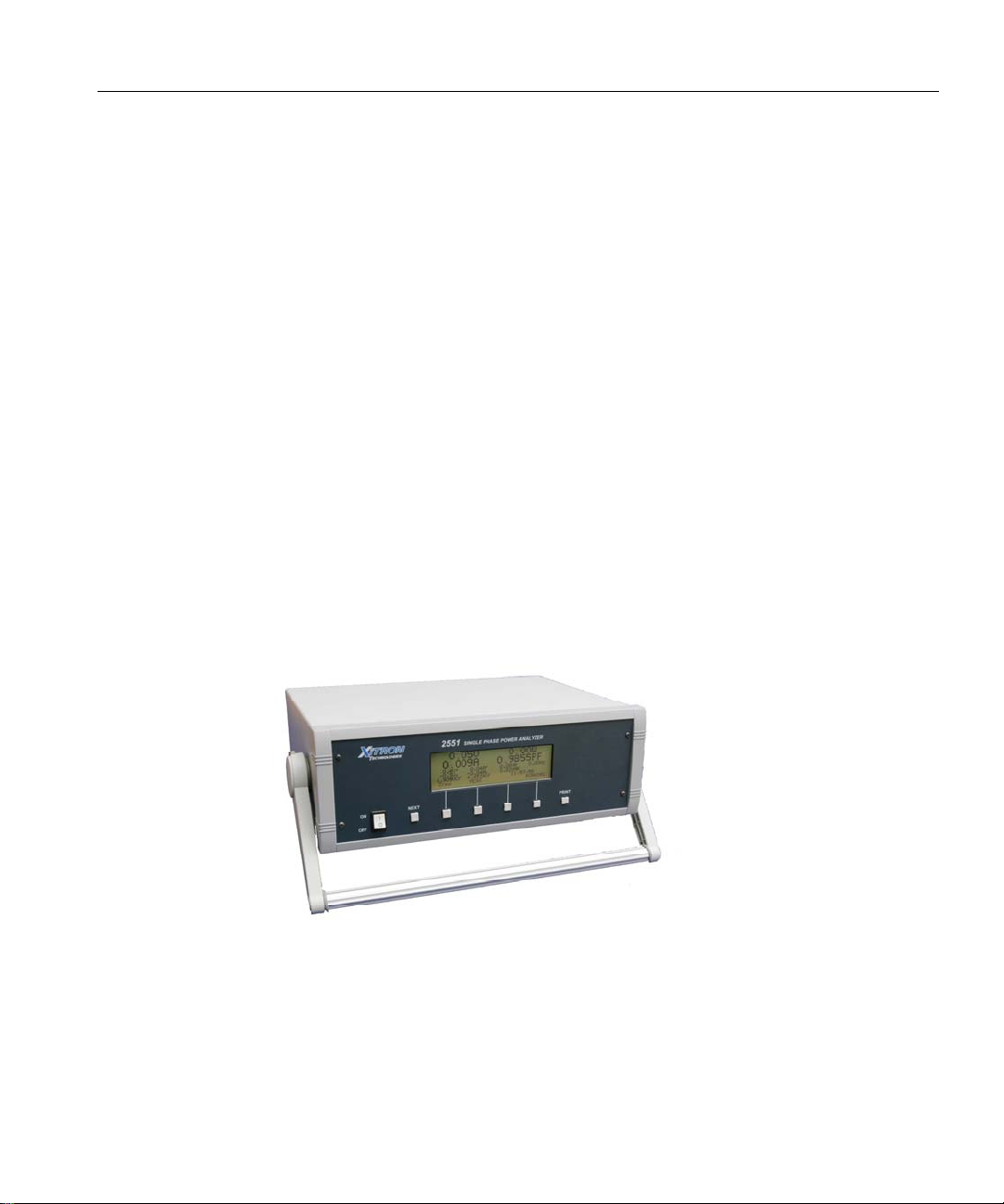
The Power Analyzer is made to sit on your bench. You can optimize the viewing angle
by adjusting the handle and optimize the viewing brightness by adjusting the DISPLAY
CONTRAST. (See Configuring the Power Analyzer page 20.)
Figure 1. Bench Type Power Analyzer
♦ To adjust the handle—
1. Press and hold the buttons located on the rear side where the handle attaches to the
case sides.
2. Rotate the handle until it clicks into place.
18 2551 User's Guide
S
WARNING: IF THE POWER ANALYZER IS USED IN A MANNER NOT SPECIFIED BY
!
XITRON TECHNOLOGIES INC., THE PROTECTION PROVIDED BY THE EQUIPMENT
MAY BE IMPAIRED.
Front Panel
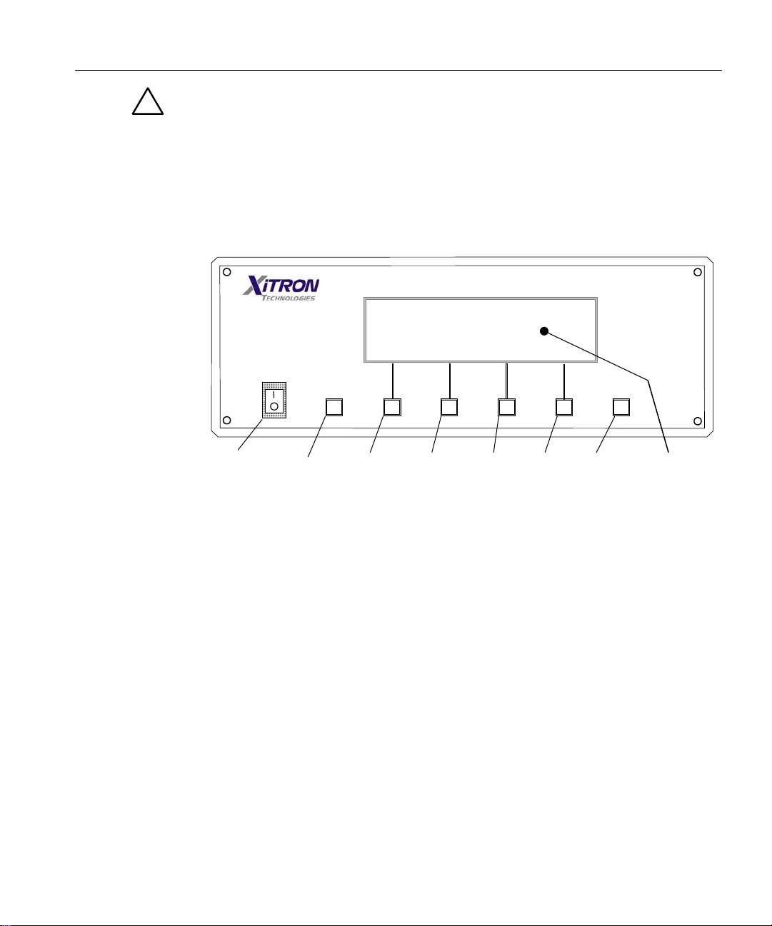
The front panel on the 2551 and 2551E includes a LCD display screen, power switch and
buttons. The buttons are from left to right: NEXT, F1, F2, F3, F4 and PRINT. See
below.
ON
OFF
Power switch
NEXT
2551
NEXT
F1
INGLE PHASE POWER ANALYZER
F2
F3
F4
PRINT
LCD display
Figure 2. Front Panel detail
The screen shows the power measurement results numerically and graphically. Refer to
Viewing Results, page 35.
The ON/OFF button powers the 2551/2551E on or off.
The NEXT button allows you to toggle through the five main display groups. Refer to
Sequence of Display Screens, page 29.
The F1 through F4 buttons (functional softkeys) allow you to select menu choices and
options. For more information, refer to Configuring the Power Analyzer page 20 and
Viewing Results page 35.
The PRINT button allows you to print a full page of data reflecting the display results. A
printout is formatted either graphically or by tabulation.
Using the Power Analyzer 19
Rear Panel Connections
!
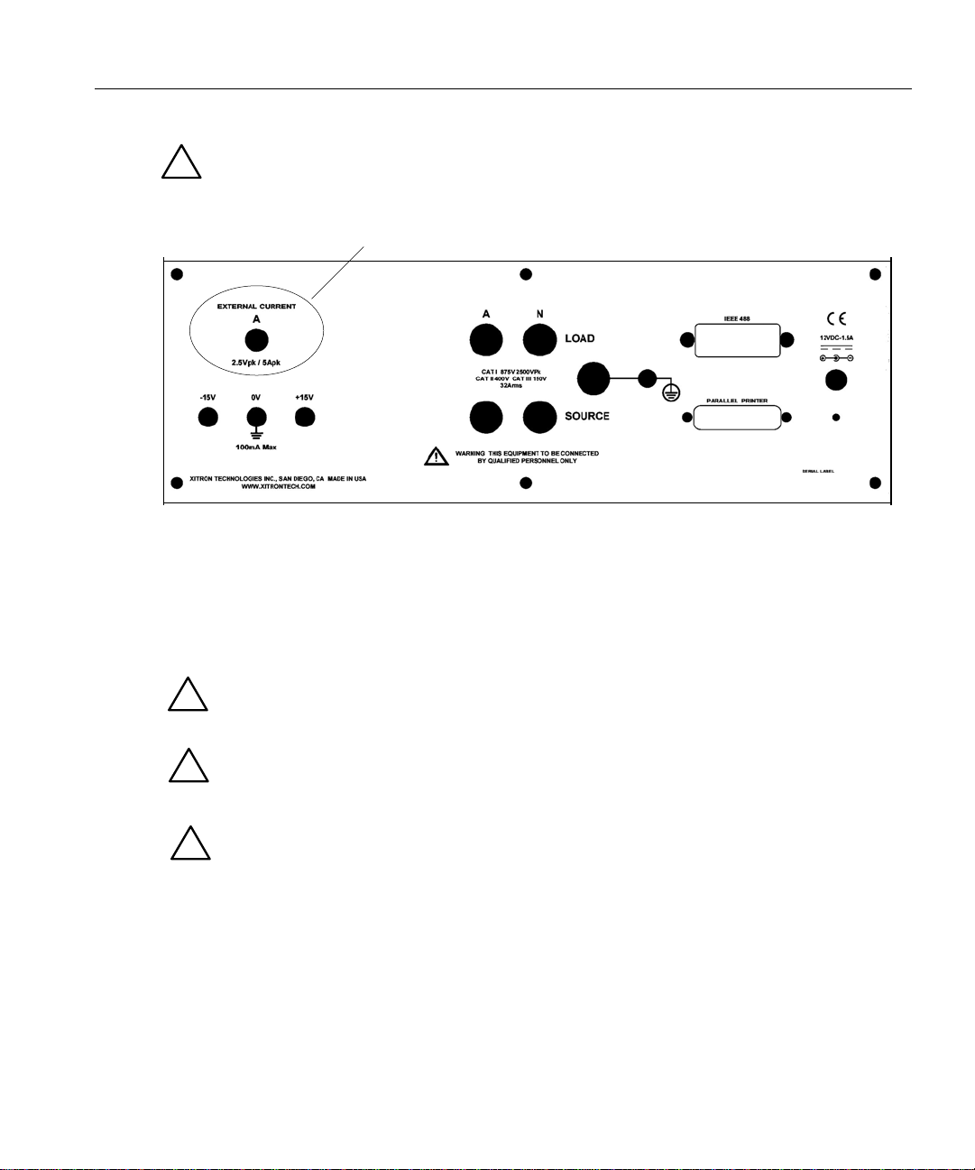
Figure 3. Rear Panel detail
The 2551/2551E rear panels provide connectors for a DC power jack, parallel printer
cable and computer interface cable. The 2551E additionally provides an external current
(BNC) connector and three transducer voltage receptacles. See below.
Available on 2551E only
♦ To power the 2551/2551E—
• Insert the 2.5mm DC power jack’s socket end of the power cord through the supplied
strain relief and into the rear panel’s 2.5mm connector. Insert the plug end of the
external power supply into an 85-265 volt AC, 47 - 400 Hz outlet.
WARNING: SHOCK HAZARD. LETHAL VOLTAGES OR CURRENT MAY BE
!
!
!
PRESENT. ENSURE NO VOLTAGE OR CURRENT EXISTS ON THESE CONNECTIONS
PRIOR TO ATTEMPTING TO CONNECT TO THESE INPUT TERMINALS.
WARNING: IT IS RECOMMENDED THAT THE PROTECTIVE CONDUCTOR
TERMINAL IS CONNECTED TO EARTH GROUND WHEN THE SIGNALS BEING
MEASURED ARE REFERENCED TO EARTH GROUND.
THE USE OF THE T5 CHARGER FROM XITRON TECHNOLOGIES OR A XITRON
TECHNOLOGIES RECOMMENDED REPLACEMENT MUST BE USED TO ENSURE
THAT THE UNIT GROUND IS NOT COMPROMISED.
♦ To connect a printer to the 2551/2551E—
• For printer interface, connect one end of your printer's cable to the PARALLEL
PRINTER port and the other to the printer.
♦ To connect a PC to the 2551/2551E—
1. Attach the computer's IEEE488 cable connector to the 24-pin socket marked
IEEE488 on the rear panel.

20 2551 User's Guide
2. On the front panel, press the NEXT button until you see the main Setup Index
3. Press CURSOR until INTERFACES/DATE/TIME is highlighted.
4. Press the SETUP button. The screen changes to the Interface Setup display.
5. Press CURSOR until the IEEE ADDRESS option is selected.
6. Press the CHANGE button until the appropriate address number displays and press
Starting the Power Analyzer
♦ To start the 2551/2551E, click the ON/OFF button to the ON position.
A startup screen will display for a few seconds. This screen lists the model number,
current and voltage input options, software revision number, and firmware installation
date and time.
display.
DONE.
Xitron 2551/2551E
Internal Current
External Current = CURRENT & VOLTAGE
Voltage Input = 950Vpk
= 8Apk
V2.6 Jun 25 2003 09:10:38
Figure 4. Startup screen
Note: If your unit is not calibrated, a WARNING statement will display along the top of
the Startup screen stating either: “ UNCALIBRATED INSTRUMENT” or
“CALIBRATION DATA HAS BEEN LOST.”
The next display you will see is the same screen that displayed when the analyzer was
last turned off.
Configuring the Power Analyzer
The Setup Index screen gives you access to separate interface configuration screens.
There is a screen for Interfaces/Date/Time; Measurements; Current Input (selection and
scaling); Calibration and one to view Product Options. Refer to Figure 5, Figure 7,
Figure 9, and Figure 11.
♦ To reconfigure the power analyzer —
1. Press the NEXT button until you see the main Setup Index screen display, as shown
below.
Using the Power Analyzer 21
Figure 5. Setup Index screen with INTERFACES/DATE/TIME selected
2. Press the CURSOR button to highlight the configuration item of choice and press
SETUP. The screen will change to display the selected item’s configuration screen.
♦ To setup the Printer and IEEE488 address interfaces and set the date and
time—
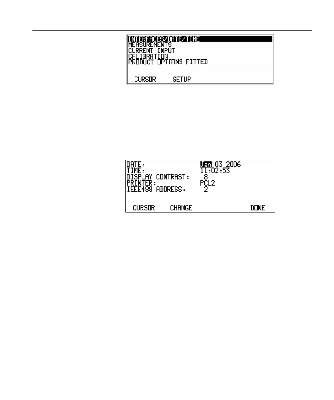
1. With INTERFACES/DATE/TIME highlighted, press the SETUP button. The
display changes to the Interface Setup display.
Figure 6. The Interface Setup screen
2. Use the CURSOR key to highlight any portion of the display that you desire to
modify. Press the CHANGE key to change the highlighted portion of the display to
the next available option for that data.
DATE = month, day, year.
TIME = (24) hours:minutes:seconds.
DISPLAY CONTRAST = 0 to 15 (default is 8)
PRINTER = PCL2; None; Text. Note that selecting None for the printer type
disables the PRINT button in all screens.
IEEE488 ADDRESS = 1 through 29
Note: If you pass an option you desire, you can come back to it by continuing to press
CURSOR.
3. Press the DONE key to save any changes made, and to return to the Setup Index
screen.
♦ To configure the measurements —
1. From the main Setup Index display, press the CURSOR button to highlight
MEASUREMENTS.
22 2551 User's Guide
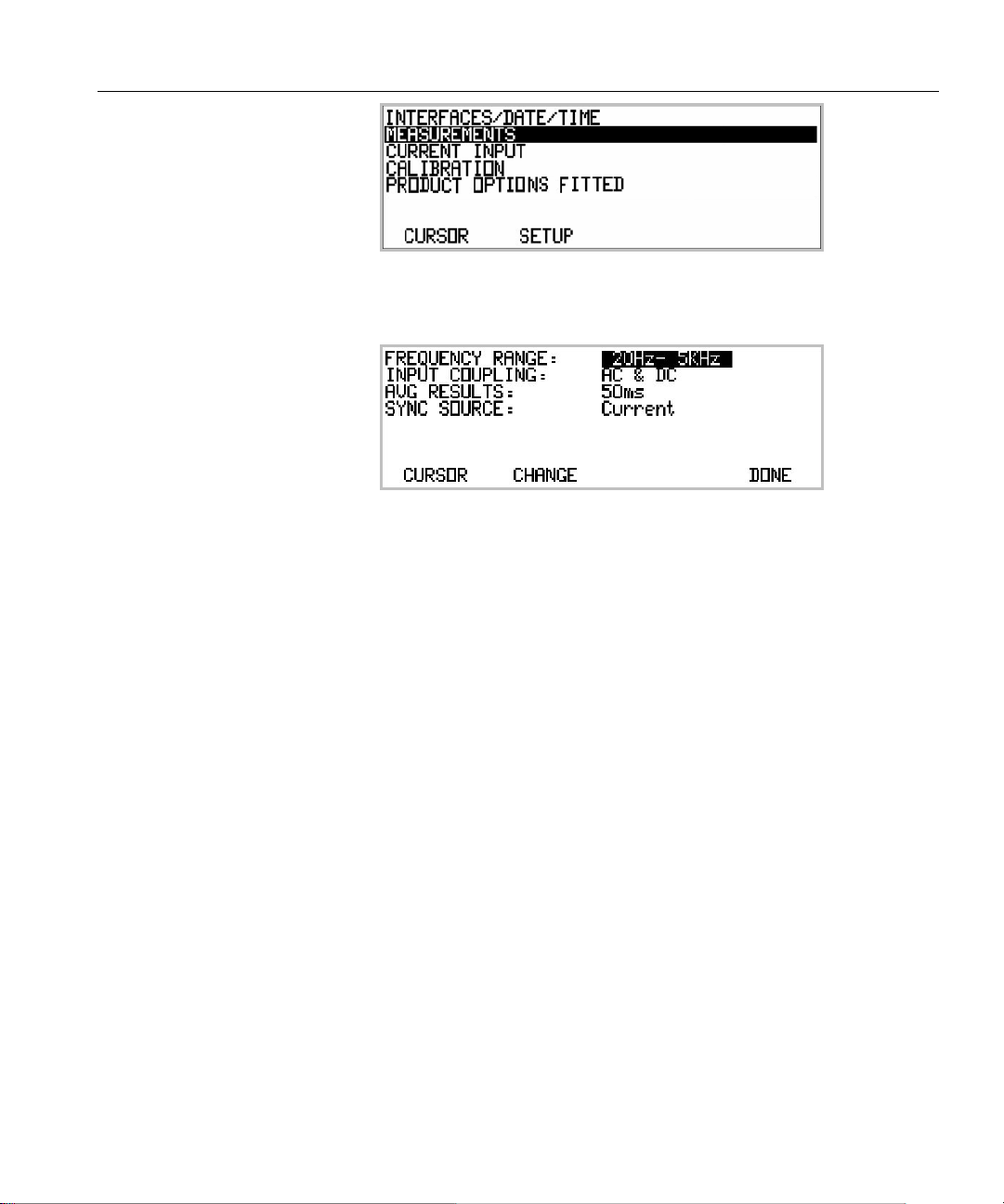
Figure 7. Setup Index screen with MEASUREMENTS selected
2. Press the SETUP button. The display changes to the Measurements Setup display.
Figure 8. The Measurement Setup screen
3. Use the CURSOR key to highlight any portion of the display that you desire to
modify. Press the CHANGE key to change the highlighted portion of the display to
the next available option for that data. The defaults are shown in bold.
FREQUENCY RANGE = .02Hz- 20Hz; 20Hz- 100KHz; 20Hz- 5KHz;
INPUT COUPLING =
AVG RESULTS =
SYNC SOURCE =
2Hz- 2KHz; 0.2Hz- 200Hz
AC & DC; AC only
50ms; 250ms; 1s; 2.5s; 5s; 10s; 20s; 1min
Voltage; Current; 50Hz; 60Hz; 400Hz; No Harmonics
4. Press the DONE key to save any changes made, and to return to the main Setup
Index screen.
♦ To configure the Current Input
The Current Input configuration screen includes selection and scaling. The current scale
allows you to scale all current readings by a numerical factor. Separate scale factors are
stored for each current input option, and are entered as transducer input:output ratio. This
scale factor may also be negative, effectively reversing the polarity of current flow.
Using the Power Analyzer 23
1. From the Setup Index display, press the CURSOR button twice. The CURRENT
INPUT choice is now highlighted as shown below.
Figure 9. Setup Index screen with CURRENT INPUT selected
2. Press the SETUP button. The display changes to the Current Input Setup display.
See example shown below.
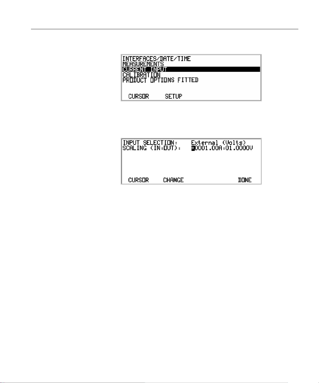
Figure 10. The Current Input Setup screen
3. Use the CURSOR key to highlight any portion of the display that you desire to
modify. Press the CHANGE key to change the highlighted portion of the display to
the next available option for that data.
INPUT SELECTION = External (Volts); Internal: External (Amps)
The scaling limits for current are within:
SCALING (IN=OUT) = +0000 .00A = 00.0000A through -9999 .99A = 99.9999A
The scaling limits for voltage are within:
SCALING (IN=OUT) = +0000 .00V = 00.0000V through -9999 .99V = 99.9999V
4. Press the DONE key to save any changes made, and to return to the Setup Index
screen. Note that the scale factor for each available current input is stored
separately.
Note: To remove DC offset and calibrate the power analyzer, refer to the Calibration
section on page 63.
24 2551 User's Guide
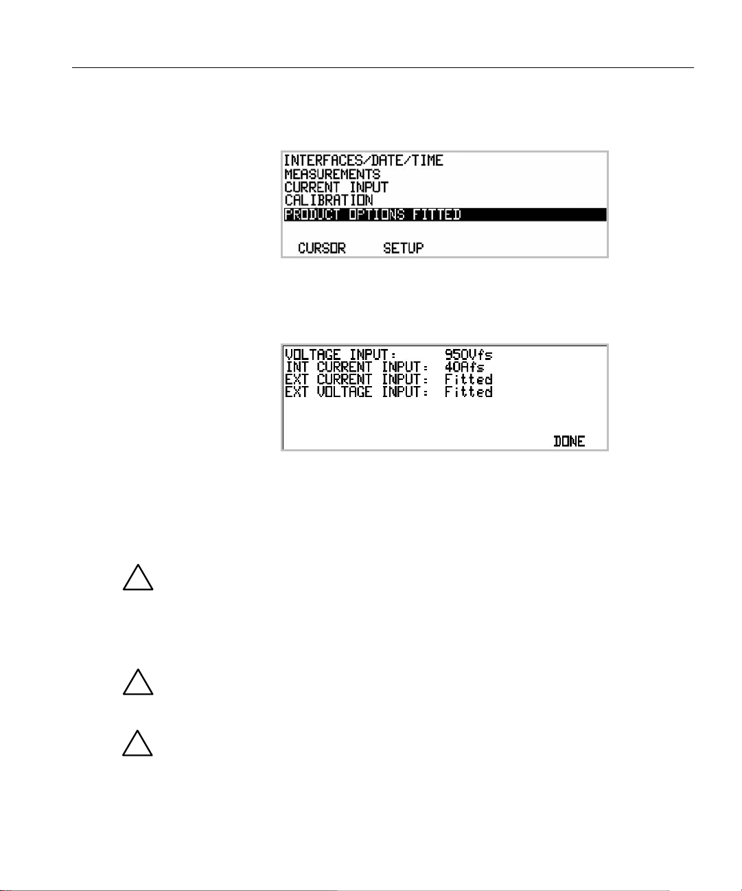
♦ To view the Option Content of your Power Analyzer
1. From the Setup Index display, press the CURSOR button four times. The
Figure 11. Setup Index screen with PRODUCT OPTIONS FITTED selected
2. Press the SETUP button. The display will show the Product Options screen. See
Figure 12. The Options Fitted screen
PRODUCT OPTIONS FITTED choice is now highlighted as shown below.
an example shown below.
3. Press the DONE k ey to return to the Setup Index screen.
Measurement Connections
WARNING: IF THE POWER ANALYZER IS USED IN A MANNER NOT SPECIFIED BY
!
!
!
XITRON TECHNOLOGIES INC., THE PROTECTION PROVIDED BY THE EQUIPMENT
MAY BE IMPAIRED.
CAUTION:
SEPARATED.
WARNING: IT IS RECOMMENDED THAT THE PROTECTIVE CONDUCTOR
TERMINAL IS CONNECTED TO EARTH GROUND WHEN THE SIGNALS BEING
MEASURED ARE REFERENCED TO EARTH GROUND.
THE USE OF THE T5 CHARGER FROM XITRON TECHNOLOGIES OR A XITRON
TECHNOLOGIES RECOMMENDED REPLACEMENT MUST BE USED TO ENSURE
THAT THE UNIT GROUND IS NOT COMPROMISED.
FOR ALL CONNECTIONS, KEEP INPUT AND OUTPUT WIRING

Using the Power Analyzer 25
Using the Internal Current Transducer
When using the internal current transducer of the power Analyzer, access the Current
Input Setup screen. Set the INPUT SELECTION to Internal and +1.0:1.0 for Scaling.
Refer to the connections shown in Figure 13.
Internal Transducer Connections for Test
Turn the source power off for the device-under-test before making each connection.
!
Attach the test device to the input terminals on the analyzer's rear panel.
Refer to the following illustration when attaching the test device.
2551
A N
LOAD
SOURCE
TEST DEVICE
USER LOAD
LINE NEUTRAL
POWER SOURCE
Figure 13. Test Device Connections
WARNING:
!
PRESENT. ENSURE NO VOLTAGE OR CURRENT EXISTS ON THESE CONNECTIONS
PRIOR TO ATTEMPTING TO CONNECT TO THESE INPUT TERMINALS.
SHOCK HAZARD. LETHAL VOLTAGES OR CURRENT MAY BE
LOAD
To measure
current
LINE (A)
A
NEUTRAL (N)
V
SOURCE
To measure
voltage
Figure 14. 2551/2551E Internal Effective Circuit (shown for reference)
 Loading...