

Page 1

Zynq-7000 AP SoC and
7 Series Devices
Memory Interface
Solutions v4.1
User Guide
UG586 November 30, 2016
Page 2

Send Feedback
Date Version Revision
• Renamed QuestaSim to Questa Advanced Simulator.
QDR II+
• Updated qdr_k_n/p directions in Physical Interface Signals table.
11/30/2016 4.1
10/05/2016 4.1
06/08/2016 4.0
04/06/2016 3.0
• Updated in qdr_k_n/p directions I/O Standards table.
RLDRAM II/RLDRAM 3
• Updated rld_dk_p/n directions in Physical Interface Signals table.
• Updated rld_dk_p/n directions in RLDRAM II I/O Standards and RLDRAM 3 Standards
tables.
• Updated to core version 4.1.
• Updated file name path to _ex/imports in all sections.
DDR3 and DDR2
• Updated Controller Options Page figure.
• Added Number of Bank Machines bullet in the Controller Options section.
DDR3 and DDR2
• Updated Memory Part description in Controller Option section.
• Added app_ecc_single_err[7:0] in Table 1-17: User Interface table.
• Added app_ecc_single_err[7:0] and note in Table 1-56: User Interface for ECC
Operation.
• Updated description in dbg_pi_phase_locked_phy4lanes and
dbg_pi_dqs_found_lanes_phy4lanes in Table 1-74: DDR2/DDR3 Debug Signals.
• Updated to core version 3.0.
• Updated Termination for all sections.
• Updated 1.0 µF capacitor in General Memory Routing Guideline chapter.
DDR3 and DDR2
• Added note in FPGA Options section.
• Added note in Interfacing to the Core section.
• Updated sys_rst descriptions in DDR3 and DD2 Configuration sections.
• Added note in Debug Signals section.
• Updated reset description in General Checks section.
Zynq-7000 AP SoC and 7 Series FPGAs MIS v4.1 2
UG586 November 30, 2016
www.xilinx.com
Page 3

Date Version Revision
Send Feedback
• Added asynchronous to sys_rst in all sections.
• Added note to RELAXED mode in DDR3/DDR2 and LDDR2 sections.
• Updated code in all Configuration sections
• Added Important jitter note in Pinout Requirements in all sections.
DDR3 and DDR2
• Added Synplify Pro Black Box Testing section.
11/18/2015 2.4
09/30/2015 2.4
06/24/2015 2.3
QDR II+
• Updated DEBUG_PORT Signal Descriptions, Write Init Debug Signal Map, and Read
Stage 1 Debug Signal Map tables.
• Updated Calibration of Read Clock and Data description.
• Updated Write Calibration description.
RLDRAM II/ RLDRAM 3
• Updated Read Stage 1 Debug Signal Map table.
• Updated Calibration of Read Clock and Data description.
• Added CLOCK_DEDICATED_ROUTE Constraints in all sections.
DDR3 and DDR2
• Updated Trace Lengths section.
QDR II+
• Added Termination section.
RLDRAM II/ RLDRAM 3
• Added Termination section.
• Updated Margin Check section.
• Updated Automatic Margin Check section.
• Updated Table 3-33: Debug Port Signals.
LPDDR2
• Updated Trace Lengths section.
Appendix
• Added General Memory Routing Guidelines.
• Added Simulation Flow Using VCS and IES to all sections.
• Added Clocking sections to QDR II+, RLDRAM II/RLDRAM 3, and LPDDR2 chapters.
RLDRAM II/ RLDRAM 3
• Added address/control signal and SSI descriptions in Pinout Requirements section.
• Updated Input Clock Guidelines section.
Zynq-7000 AP SoC and 7 Series FPGAs MIS v4.1 3
UG586 November 30, 2016
www.xilinx.com
Page 4

Date Version Revision
Send Feedback
• Updated description in all Configuration sections.
• Updated SIM_BYPASS_INIT_CAL.
Chapter 1
• Added description in Setting DDR3 Memory Parameter Option section.
• Added Note to Answer Record: 54025 in Controller Options section.
• Added description to app_rd_data_end in Table 1-17: User Interface.
• Updated Table 1-19: AXI4 Slave Interface Parameters.
• Updated description in AXI4 Slave Interface Signals section.
• Updated Time Division Multiplexing (TDM), Round-Robin, and Read Priority
(RD_PRI_REG) sections.
• Updated GES description in Calibration Times section.
• Updated Fig. 1-50: Clocking Architecture.
• Updated Table 1-87: Memory Controller to Calibration Logic Interface Signals.
• Updated AXI Addressing section.
• Updated Write Path section.
• Updated Fig. 1-84: Command Processing.
04/01/2015 2.3
Continued
• Updated Physical Layer Interface (Non-Memory Controller Design) section.
• Updated CK signal description in Trace Length section.
• Updated Fig. 1-93: Calibration Stages.
• Updated description in Determine the Failing Calibration Stage section.
• Updated Table 1-100: DDR2/DDR3 Debug Signals.
• Updated Table 1-102: Debug Signals of Interest for Write Leveling Calibration.
• Updated Table 1-103: Debug Signals of Interest for MPR Read Leveling Calibration.
• Updated calibration overview in Debugging OCLKDELAYED Calibration Failures
section.
• Updated Debug bullets in Debugging OCLKDELAYED Calibration Failures section.
• Updated Table 1-104: Debug Signals of Interest for OCLKDELAYED Calibration to
Table 1-106: Debug Signals of Interest for Read Leveling Stage 1 Calibration.
• Updated Table 1-108: Calibration Time in Hardware.
• Updated Checking and Varying Read Timing to Manual Window Check sections.
• Updated Calibration Times section.
Chapter 2
• Updated Fig. 2-43: High-Level PHY Block Diagram for a 36-Bit QDR II+ Interface.
• Updated Margin Check and Automated Margin Check sections.
Chapter 3
• Updated description in Interfacing with the Core through the Client Interface section.
Chapter 4
• Corrected app_wdf_data[APP_DATA_WIDTH – 1:0] and
app_wdf_mask[APP_MASK_WIDTH – 1:0] sections.
• Updated Fig. 4-43: Clocking Architecture.
• Updated Read Path section.
Zynq-7000 AP SoC and 7 Series FPGAs MIS v4.1 4
UG586 November 30, 2016
www.xilinx.com
Page 5

Date Version Revision
Send Feedback
Chapter 1
• Updated description in Round-Robin section.
• Updated RTT_WR in Table 1-92: 7 Series FPGA Memory Solution Configuration
Parameters.
11/19/2014 2.3
10/01/2014 2.2
Continued
• Updated description in Debugging OCLKDELAYED Calibration Failures section.
• Updated Table 1-106: Debug Signals of Interest for OCLKDELAYED Calibration.
•Updated GES time in Calibration Times section.
• Updated bits in left_loss_pb and right_gain_pb in Table 1-109: Debug Signals of
Interest for PRBS Read Leveling Calibration.
• Global update to example design link in Files in example_design/sim Directory tables,
updated links in Simulation Flow Using IES and VCS Script Files section, updated
Simulation Flow Using Vivado Simulator section, and updated Simulation Flow Using
QuestaSim section.
Chapter 1
• Updated Reference Clock description in FPGA Option section.
• Updated C_S_AXI_DATA_WIDTH description in Table 1-19: AXI4 Slave Interface
Parameters.
• Updated Fig. 1-50: Clocking Architecture.
• Updated OCLKDELAYED Calibration section.
• Updated Write Path section.
• Added REF_CLK_MMCM_IODELAY_CTRL in Table 1-92: 7 Series FPGA Memory
Solution Configuration Parameters.
• Added note for nBANK_MACHS in Table 1-93: Embedded 7 Series FPGAs Memory
Solution Configuration Parameters.
• Added row and updated Table 1-94: DDR2/DDR3 SDRAM Memory Interface Solution
Pinout Parameters
• Updated CK/CK# bullet in Trace Length section.
• Updated Table 1-102: DDR2/DDR3 Debug Signals.
• Updated debug signals in Table 1-112: Debug Signals Used for Checking and Varying
Read/Write Timing.
Chapter 2
• Added Bank Sharing Among Controllers section in Design Guideline section.
Chapter 3
• Added Bank Sharing Among Controllers section in Design Guideline section.
Chapter 4
• Updated Figs. 4-57 to 4-59 and Figs. 4-62 to 4-63.
• Updated 2:1 description in Write Path section.
• Updated rules in Termination section.
Zynq-7000 AP SoC and 7 Series FPGAs MIS v4.1 5
UG586 November 30, 2016
www.xilinx.com
Page 6

Date Version Revision
Send Feedback
Chapter 1
• Added reference to data sheet in Features section.
• Added Important note about Data Mask in Controller Options section.
• Added note in Precharge Policy section.
• Added PRBS_SADDR_ MASK)POS to Table 1-11: Traffic Generator Parameters Set in
the example_top Module.
• Updated IDELAYCTRL frequency in IDELAYCTRL section.
• Updated IDELAY Reference Clock section.
• Updated PRBS Read Leveling section.
• Updated CL description for DDR3 in Table 1-93: Embedded 7 Series FPGAs Memory
Solution Configuration Parameters.
• Updated package length descriptions in Trace Length section.
• Added simulation description in Note in Debugging DDR3/DDR2 Designs.
• Updated description in Debugging PRBS Read Leveling Failures section.
06/04/2014 2.1
Continued
• Updated Table 109: Debug Signals of Interest for PRBS Read Leveling Calibration.
Chapter 2
• Added reference to data sheet in Introduction section.
• Updated package length descriptions in Trace Length Requirements section.
• Added CPT_CLK_SEL_* row in Table 2-11: QDR II+ SRAM Memory Interface Solution
Pinout Parameters.
• Added simulation description in Note in Debugging QDR II+ Designs.
Chapter 3
• Added reference to data sheet in Features section.
• Added note in Memory Controller section.
• Added PRBS_SADDR_ MASK)POS to Table 3-8: Traffic Generator Parameters Set in the
example_top Module.
• Updated rules and package length descriptions in Trace Length Requirements
section.
• Added simulation description in Note in Debugging RLDRAM II and 3 Designs.
Chapter 4
• Added note in Precharge Policy section.
• Added PRBS_SADDR_ MASK)POS to Table 4-11: Traffic Generator Parameters Set in
the example_top Module.
• Updated package length descriptions in Trace Length Requirements section.
• Added simulation description in Note in Read Path section.
Zynq-7000 AP SoC and 7 Series FPGAs MIS v4.1 6
UG586 November 30, 2016
www.xilinx.com
Page 7

Date Version Revision
Send Feedback
Chapter 1
• Updated book to DQS.
• Updated Table 1-4: Files in example_design/sim Directory.
• Updated file description in Simulation Flow Using IES and VCS Script Files section.
• Added No Buffer description in the System Clock bullet in FPGA Options section.
• Updated mc_data_offset description in Memory Controller to Calibration Logic
Interface Signals table.
• Added MPR read leveling process in Multi-Purpose Register Read Leveling section.
• Updated Temperature Monitor section.
• Added tempmon information in Physical Layer Interface (Non-Memory Controller
Design) section.
• Added description in address and control signals in Termination section for DDR3.
• Added description in address and control signals and updated CKE signal bullet in
Termination section for DDR2.
• Added CK description in Trace Lengths section.
• Added new code constraints for DDR3/DDR2 Configuration sections.
04/02/2014 2.0
• Added Clocking section.
• Updated ocal signals in Table 1-102: DDR2/DDR3 Debug Signals.
Chapter 2
• Added new code constraints in Configuration section.
• Updated Table 2-3: Files in example_design/sim Directory.
• Updated file description in Simulation Flow Using IES and VCS Script Files section.
Chapter 3
• Added new code constraints in Configuration section.
• Updated Table 3-3: Files in example_design/sim Directory.
• Added important note on write and read commands in Interfacing with the Core
through the Client Interface section.
• Updated option for MRS_RD_LATENCY in RLDRAM II Memory Interface Solution
Configurable Parameters table.
• Updated file description in Simulation Flow Using IES and VCS Script Files section.
Chapter 4
• Added new code constraints in Configuration section.
• Updated Table 4-4: Files in example_design/sim Directory.
• Updated file description in Simulation Flow Using IES and VCS Script Files section.
Zynq-7000 AP SoC and 7 Series FPGAs MIS v4.1 7
UG586 November 30, 2016
www.xilinx.com
Page 8

Date Version Revision
Send Feedback
• Vivado Design Suite release only for MIG v2.0.
Chapter 1
• Added Out of Context content.
• Updated Table 1-4: Modules in example_design/sim Directory.
• Updated <component name>/user_design section.
• Updated Fig. 1-39: Synthesizable Example Design Block Diagram.
• Added simulator flows.
• Added Bits[39:32] to Table 1-15: Debug Status for the Write Transaction.
• Added Bits[39:32] to Table 1-16: Debug Status for the Read Transaction.
• Added OOC description in Customizing the Core section.
• Added ILA trigger settings in Vivado Lab Tools section.
• Added note on read latency in Debug section.
• Updated Chipscope triggers to R in Debug section.
Chapter 2
• Added Out of Context content.
• Updated Table 2-3: Modules in example_design/sim Directory.
• Updated <component name>/user_design section.
• Added OOC description in Customizing the Core section.
• Added simulator flows.
12/18/2013 2.0
• Added ILA trigger settings in Vivado Lab Tools section.
Chapter 3
• Added Out of Context content.
• Updated Table 3-3: Modules in example_design/sim Directory.
• Updated <component name>/user_design section.
• Updated Fig. 3-35: Synthesizable Example Design Block Diagram.
• Added OOC description in Customizing the Core section.
• Added simulator flows.
• Added ILA trigger settings in Vivado Lab Tools section.
• Updated Fig. 3-48 Write Path Block Diagram of the RLDRAM II Interface Solution.
• Added note on read latency in Debug section.
Chapter 4
• Added Out of Context content.
• Updated Table 4-4: Modules in example_design/sim Directory.
• Updated <component name>/user_design section.
• Updated Fig. 4-37: Synthesizable Example Design Block Diagram.
• Added OOC description in Customizing the Core section.
• Added simulator flows.
• Added note on read latency in Debug section.
Chapter 5
• Added Out of Context content.
Zynq-7000 AP SoC and 7 Series FPGAs MIS v4.1 8
UG586 November 30, 2016
www.xilinx.com
Page 9

Date Version Revision
Send Feedback
• Vivado Design Suite release only for MIG v2.0.
• Removed ISE content throughout book and updated screenshots to v2.0.
Chapter 1
• Updated Memory Part bullet description.
• Updated Table 1-4 sim.do description and simulation directory.
• Updated Fig. 1-44 7 Series FPGAs MIS.
• Added aresetn in Table 1-20 AXI4 Slave Interface Signals.
• Added Caution note in Single Error and Double Error Reporting section.
• Updated Table 1-77 Memory Interface Commands.
• Updated and added stage 3 tap in OCLKDELAYED Calibration section.
• Added #4 table note to Table 1-91 7 Series FPGA Memory Solution Configuration
Parameters.
• Updated description in app_wdf_mask[APP_MASK_WIDTH - 1:0] section.
• Added Memory Address Mapping description in User Interface section.
• Updated Table 1-106 Debug Signals of Interest for OCLKDELAYED Calibration
Chapter 2
10/02/2013 2.0
• Updated Table 2-3 sim.do description and simulation directory.
• Updated DIFF_HSTL_I in I/O Standards table.
• Updated reference clock descriptions in Clocking Architecture section.
• Added #1 table note to Table 2-11 7 Series FPGAs QDR II+ SRAM Memory Interface
Solution Configurable Parameters. And updated SIM_BYPASS_INIT_CAL.
Chapter 3
• Updated Table 3-3 sim.do description and simulation directory.
• Updated reference clock descriptions in Clocking Architecture section.
• Added #1 table note to Table 3-13 RLDRAM II Memory Interface Solution
Configurable Parameters. And updated SIM_BYPASS_INIT_CAL.
Chapter 4
• Updated Table 4-4 sim.do description and simulation directory.
• Updated Fig. 4-37 7 Series FPGAs MIS.
• Updated Table 4-14 User Interface.
• Added #4 note to Table 4-25 7 Series FPGA Memory Solution Configuration
Parameters.
• Updated description in app_wdf_mask[APP_MASK_WIDTH - 1:0] section.
• Added Memory Address Mapping description in User Interface section.
Zynq-7000 AP SoC and 7 Series FPGAs MIS v4.1 9
UG586 November 30, 2016
www.xilinx.com
Page 10

Date Version Revision
Send Feedback
• Vivado Design Suite release only for MIG v2.0. Revision number advanced to 2.0 to
align with core version number.
Chapter 1
• Updated ChipScope to Vivado logic analyzer, VIO, and ILA.
• Updated ui_clk and ui_clk_sync_rst descriptions in Table 1-17 User Interface.
• Updated ui_clk and ui_clk_sync_rst descriptions.
• Added Ordering Modes in Reordering section and added modes in Table 1-91.
• Updated ECC enable in AXI4 Slave Interface Block section.
• Updated Read Priority (RD_PRI) section.
• Updated Table 1-19 AXI4 Slave Interface Parameters, C_S_AXI_ADDR_WIDTH value
and descriptions.
• Added Write Priority description.
• Updated PHASER_IN DQSFOUND Calibration section.
•Removed Downsizing Option.
• Added DM in DQ descriptions.
• Added Dynamic Calibration and Periodic Read Behavior section.
• Added Vivado Lab Tools section.
• Added AR 54025 for Vivado.
• Updated Debugging PHASER_IN DQSFOUND Calibration Failures
06/19/2013 2.0
(dbg_pi_dqsfound_err = 1) section.
Chapter 2
• Updated ChipScope to Vivado logic analyzer, VIO, and ILA.
• Added Fixed Latency Mode description in Controller Options section.
• Removed qdr_qvld in Table 2-12 Physical Interface Signals.
• Updated Figure 2-26 Four-Word Burst Length Memory Device Protocol.
• Updated Output Architecture section in Write Path.
• Added Write Calibration section.
•Removed QVLD.
• Updated Table 2-20 Write Init Debug Signal Map.
• Updated Tables 2-21 and 2-22 Read Stage 1 and Stage 2 Debug Signal Map tables.
Chapter 3
• Updated ChipScope to Vivado logic analyzer, VIO, and ILA.
• Removed rld_qvld in Table 3-13 Physical Interface Signals.
• Removed QVLD and QVLD_MAP in Table 3-16 RLDRAM II Memory Interface Solution
Pinout Parameters.
•Removed QVLD.
• Updated descriptions in Manual Pinout Changes section.
• Added new calibration description in Calibration section.
• Updated Table 3-26 Physical Layer Simple Status Bus Description Defined in the
rld_phy_top Module.
Zynq-7000 AP SoC and 7 Series FPGAs MIS v4.1 10
UG586 November 30, 2016
www.xilinx.com
Page 11

Date Version Revision
Send Feedback
• Updated Table 3-27 DEBUG_PORT Signal with
dbg_rd_stage1_rtr_error[N_DATA_LANES - 1:0] and
dbg_rd_stage1_error[N_DATA_LANES - 1:0].
• Updated Tables 3-31 and 3-32 Read Stage 1 and Stage 2 Debug Signal Map tables.
• Added Fig. 3-36 Calibration Flow Diagram and Fig. 3-37 Read Level Stage 1.
• Added description to Data Alignment and Valid Generation section.
• Updated description and added Figs. 3-38 to 3-43 in Write Calibration section.
• Added Write Calibration Debug Map section.
Continued
03/20/2013 1.9
Chapter 4
• Updated ChipScope to Vivado logic analyzer, VIO, and ILA.
• Updated ui_clk and ui_clk_sync_rst descriptions in Table 4-14 User Interface.
• Updated ui_clk and ui_clk_sync_rst descriptions.
• Added Ordering Modes in Reordering section and added modes in Table 4-25.
• Added DM in DQ descriptions.
• Added Termination description in LPDDR2 Pinout Examples section.
Chapter 6
• Added Upgrading the ISE/CORE Generator MIG Core in Vivado section.
• ISE 14.5 and Vivado Design Suite 2013.1 releases for MIG v1.9 and v1.9a.
Chapter 1
• Added Memory Part frequency in Controller Options section.
• Added No Buffer option description in FPGA Options section.
• Added pinout description in Verify Pin Changes and Update Design section.
• Updated Fig. 1-15 Setting Memory Mode Options.
• Updated Fig. 1-16 FPGA Options.
• Updated Fig. 1-30 7 Series FPGAs Memory Interface Solution to User’s FPGA Logic
• Added ECC description in AXI4 Slave Interface Block section.
• Updated Table 1-91 7 Series FPGA Memory Solution Configuration Parameters.
• Updated Table 1-92 Embedded 7 Series FPGAs Memory Solution Configuration
Parameters.
• Updated Table 1-93 DDR2/DDR3 SDRAM Memory Interface Solution Pinout
Parameters.
• Added description in Verifying the Simulation Using the Example Design section.
• Reworked Design Guidelines DDR3 SDRAM section.
• Added new debug section.
Zynq-7000 AP SoC and 7 Series FPGAs MIS v4.1 11
UG586 November 30, 2016
www.xilinx.com
Page 12

Date Version Revision
Send Feedback
Chapter 2
• Added No Buffer option description in FPGA Options section.
• Added pinout description in Verify Pin Changes and Update Design section.
• Updated Fig. 2-15 FPGA Options.
• Updated REFCLK_FREQ and RST_ACT_LOW in Table 2-13 7 Series FPGAs QDR II+
SRAM Memory Interface Solution Configurable Parameters
• Updated Table 2-14 QDR II+ SRAM Memory Interface Solution Pinout Parameters.
• Added description in Verifying the Simulation Using the Example Design section.
Chapter 3
• Added No Buffer option description in FPGA Options section.
Continued
• Updated Fig. 3-14 FPGA Options.
• Added Verify Pin Changes and Update Design section.
• Updated nCK_PER_CLK in Table 3-10 Traffic Generator Parameters Set in the
example_top Module
• Updated Table 3-15 RLDRAM II Memory Interface Solution Configurable Parameters.
• Updated Table 3-16 RLDRAM II Memory Interface Solution Pinout Parameters.
• Added description in Verifying the Simulation Using the Example Design section.
Chapter 4
• Added new LPDDR2 SDRAM section.
Chapter 6
• Updated to new GUIs.
Zynq-7000 AP SoC and 7 Series FPGAs MIS v4.1 12
UG586 November 30, 2016
www.xilinx.com
Page 13

Date Version Revision
Send Feedback
• ISE 14.4 and Vivado 2012.4 Design Suite releases for MIG v1.8.
Chapter 1
• Updated Table 1-2 to 1-9 with new table note and.v name.
• Updated Fig. 1-16 FPGA Options GUI.
• Added XADC Instantiation bullet.
• Added description to sim.do in Table 1-4.
• Updated Table 1-11 DATA_PATTERN to 0xA.
• Updated Table 1-13 vio_data_mode_value[3:0] to 0xA.
• Updated description in Setting Up for Simulation.
• Added description to EDK Clocking.
• Updated ui_clk and ui_clk_sync_rst in Table 1-17.
• Added description in Internal (FPGA) Logic Clock.
• Added TEMP_MON_CONTROL to Table 1-91.
• Added DATA_IO_IDLE_PWRDWN and CA_MIRROR to Table 1-92.
• Added HP bank description in Bank and Pin Selection Guides for DDR3 Designs.
• Added DDR3 SDRAM interface description to Configuration.
• Added HP bank description in Bank and Pin Selection Guides for DDR2 Designs.
• Added DDR2 SDRAM interface description to Configuration.
12/18/2012 1.8
Chapter 2
• Updated Table 2-2 and 2-7 to 2-8 with new table note and.v name.
• Added description to sim.do in Table 2-3.
• Updated descriptions and added Fig 2-26 to Clocking Architecture.
• Updated description in Write Path Output Architecture.
• Updated descriptions in Trace Length Requirements.
• Added QDRII description in Configuration.
• Added description to Verifying the Simulation Using the Example Design.
• Added Margin Check and Automated Margin Check sections.
Chapter 3
• Updated Table 3-2 and 3-6 to 3-8 with new table note and.v name.
• Added description to sim.do in Table 3-3.
• Updated Table 3-10 DATA_PATTERN to 0xA.
• Updated descriptions and added Fig 3-30 to Clocking Architecture.
• Updated descriptions in Trace Length Requirements.
• Added descriptions in RLDRAM II.
• Added RLDRAM II description in Configuration.
• Added description to Verifying the Simulation Using the Example Design.
• Added Debug section.
Zynq-7000 AP SoC and 7 Series FPGAs MIS v4.1 13
UG586 November 30, 2016
www.xilinx.com
Page 14

Date Version Revision
Send Feedback
• MIG 1.7 release. Updated ISE Design Suite version to 14.3.
• Chapter 1: Added AXI4-Lite Slave Control/Status Register Interface Block section.
Updated figures (1-32 and 1-37) and added PRBS and Temperature Monitor sections.
Added CLKIN_PERIOD to USE_DM_PORT parameters in Table 1-37. Updated Table
1-38 PHY0_BITLANES description.
• Chapter 2: Added CLKIN_PERIOD to DIVCLK_DIVIDE parameters in Table 2-13.
10/16/2012 1.7
07/25/2012 1.6
06/13/2012 1.5
• Chapter 3: Added RLDRAM 3 content throughout. Updated/added figures (3-10,
3-13, 3-23 to 3-32, 3-36 to 3-37, 3-40 to 3-41, 3-45 to 3-47, and 3-50). Added
mem_ck_lock_complete parameter in Table 3-11. Added CLKOUT0_PHASE parameter
in Table 3-15. Updated descriptions in Table 3-16 and added Table 3-28. Updated
Table 3-29 user_cmd signal. Updated Table 3-31 and 3-34 descriptions. Added
Debugging Write Calibration section.
• Chapter 4: Added System Clock Sharing section
• Chapter 5: Updated figures (5-15, 5-17 to 5-20), updated steps in Getting Started with
Vivado – MIG IP Generation
• MIG 1.6 release. Updated ISE Design Suite version to 14.2. Updated GUI screen
captures throughout document.
• Chapter 1: Added No Buffer, Use System Clock, and Sample Data Depth in FPGA
Options, page 36. Changed the parameters nCK_PER_CLK, tZQI, SYSCLK_TYPE,
REFCLK_TYPE, and APP_DATA_WIDTH. Added bulleted item about multiple CK
outputs to Bank and Pin Selection Guides for DDR3 Designs, page 186. Updated Trace
Lengths, page 191 and Termination, page 200.
• Chapter 2: Added No Buffer, Use System Clock, and Sample Data Depth in FPGA
Options, page 282. Changed the parameters SYSCLK_TYPE and REFCLK_TYPE.
• Chapter 3: Added No Buffer, Use System Clock, and Sample Data Depth in FPGA
Options, page 282. Changed the parameters SYSCLK_TYPE and REFCLK_TYPE.
• Chapter 6: Added new chapter on migrating to Vivado Design Suite.
Revised the recommended total electrical delay on CK/CK# relative to DQS/DQS# on
page 191.
Zynq-7000 AP SoC and 7 Series FPGAs MIS v4.1 14
UG586 November 30, 2016
www.xilinx.com
Page 15

Date Version Revision
Send Feedback
• MIG 1.5 release. Updated ISE Design Suite version to 14.1. Updated GUI screen
captures throughout document. Replaced IODELAYCTRL with IDELAYCTRL
throughout.
• Chapter 1: Added I/O Power Reduction option to FPGA Options. Revised I/O
standards for sys_rst option in Bank Selection. Added Creating ISE Project Navigator
Flow for MIG Example Design, Power-Saving Features, Multi-Purpose Register Read
Leveling, OCLKDELAYED Calibration, Upsizing, and External Vref sections. Changed
bits [16:15] to from Rank Count to Reserved in the PHY Control word. Revised
maximum setting of NUM_DQ_PINS in Table 1-11. Revised Figure 1-55 flowchart.
Removed RankSel[1:0] from Figure 1-56 and Figure 1-58. Added mc_odt and mc_cke
to Table 1-87. Replaced AXI Addressing. Updated REFCLK_FREQ, RANK_WIDTH, and
WRLVL in Table 1-92. Added DATA_IO_PRIM_TYPE to Table 1-93. Added bullet about
04/24/2012 1.4
01/18/2012 1.3
DQS pins to Bank and Pin Selection Guides for DDR3 Designs. Changed DIFF_SSTL_15
to DIFF_SSTL18_II and SSTL15 to SSTL18_II.
• Chapter 2: Changed DIFF_SSTL_15 to DIFF_HSTL_I and SSTL15 to HSTL_I. Revised I/O
standards for sys_rst option in System Pins Selection. Revised the PHY_BITLANE
parameters in Table 2-11. Added System Clock, PLL Location, and Constraints and
Configuration sections.
• Chapter 3: Changed DIFF_SSTL_15 to DIFF_HSTL_I and SSTL15 to HSTL_I. to Revised
I/O standards for sys_rst option in System Pins Selection. Added the Write
Calibration, System Clock, PLL Location, and Constraints, and Configuration sections.
Revised the PHY_BITLANE parameters in Table 3-15. In Table 3-28, added
dbg_wrcal_sel_stg[1:0], dbg_wrcal[63:0], dbg_wrcal_done[2:0],
dbg_wrcal_po_first_edge[5:0], dbg_wrcal_po_second_edge[5:0], and
dbg_wrcal_po_final[5:0].
• MIG 1.4 release. Updated ISE Design Suite version to 13.4. Updated GUI screen
captures throughout document.
• Chapter 1: Added support for DDR2 SDRAM. Added option 3 to MIG Output Options.
Added EDK Clocking. Added Replaced Figure 1-41 and Figure 1-69.
• Chapter 2: Removed Input Clock Period option from Controller Options. Added
Memory Options. Added Reference Clock option to FPGA Options. Updated Debug
Signals.
• Chapter 3: Removed Input Clock Period option from Controller Options. Added Input
Clock Period option to Memory Options. Added Reference Clock option to FPGA
Options. Added Debugging RLDRAM II and RLDRAM 3 Designs.
Zynq-7000 AP SoC and 7 Series FPGAs MIS v4.1 15
UG586 November 30, 2016
www.xilinx.com
Page 16

Date Version Revision
Send Feedback
• MIG 1.3 release. Updated ISE Design Suite version to 13.3.
• Chapter 1: Added step 2 to MIG Output Options, page 26. Added note about
optional use of the memory controller to Controller Options, page 30. Added
arbitration scheme to AXI Parameter Options, page 33. Added description of DCI
Cascade under Figure 1-23. Updated text about devices with SSI technology and SLRs
on page 41 and page 187. Changed error to tg_compare_error on page 42. Replaced
Table 1-8. Added qdr_wr_cmd_o, vio_fixed_instr_value, vio_fixed_bl_value,
vio_pause_traffic, and vio_data_mask_gen signals to Table 1-13. Added signals to the
User Interface in Figure 1-49 and Figure 1-51. Added app_sr_req, app_sr_active,
app_ref_req, app_ref_ack, app_zq_req, and app_zq_ack signals to Table 1-17. Added
app_wdf_rdy, app_ref_req, app_ref_ack, app_zq_req, app_zq_ack, Read Priority with
Starve Limit (RD_PRI_REG_STARVE_LIMIT), Native Interface Maintenance Command
Signals, User Refresh, and User ZQ sections. Added C_RD_WR_ARB_ALGORITHM to
Table 1-19. Updated fields in Table 1-84, changed Hi Index (Rank) to Rank Count, and
added CAS slot field. Updated AXI Addressing and Physical Layer Interface
(Non-Memory Controller Design). Added Figure 1-75 through Figure 1-77 in Write
Path. In Table 1-92, removed DISABLED option from RTT_NOM for DDR3_SDRAM,
changed RTT_NOM to RTT_WR in RTT_WR, updated SIM_BYPASS_INIT_CAL, and
updated table note 2. In Table 1-93, updated tZQI and added USER_REFRESH. Added
Table 1-94. In Configuration, updated constraints example and removed paragraph
10/19/2011 1.2
about SCL and SDA.
• Chapter 2: Added step 2 to MIG Output Options, page 275. Added Input Clock Period
description in Controller Options, page 279. Added Debug Signals Control and
Internal Vref Selection options to FPGA Options, page 282. Added I/O Planning
Options, page 285. In System Pins Selection, page 288, changed cal_done signal to
init_calib_complete and error signal to tg_compare_error. Replaced Table 2-2.
Changed file names in Table 2-5. Updated signal names in Figure 2-38, Figure 2-39,
and Figure 2-40. Updated signal names in Table 2-7. Added CPT_CLK_CQ_ONLY and
updated value for SIM_BYPASS_INIT_CAL in Table 2-10. Added Table 2-11. Updated
pinout rules in Pinout Requirements, page 337. Added paragraph about DCI and
IN_TERM after Table 2-12. Added Debugging QDR II+ SRAM Designs, page 340.
• Chapter 3: Added step 2 to MIG Output Options, page 375. Added Input Clock Period
description in Controller Options. Added Debug Signals Control and Internal Vref
Selection options to FPGA Options, page 382. In System Pins Selection, changed
cal_done signal to init_calib_complete and error signal to tg_compare_error. Changed
file names in Table 3-6. Removed Table 3-12, which contained Reserved signals not
used. Added rst_phaser_ref to Table 3-11. Removed PHY-Only Interface section. In
Table 3-14, added RLD_ADDR_WIDTH, MEM_TYPE, CLKIN_PERIOD, and SIMULATION,
and renamed CLKFBOUT_MULT, CLKOUT0_DIVIDE, CLKOUT1_DIVIDE,
CLKOUT2_DIVIDE, and CLKOUT3_DIVIDE. Updated Table 3-15. Added paragraph
about DCI and IN_TERM after Table 3-24.
• Added Chapter 5, Multicontroller Design.
Zynq-7000 AP SoC and 7 Series FPGAs MIS v4.1 16
UG586 November 30, 2016
www.xilinx.com
Page 17

Date Version Revision
Send Feedback
• MIG 1.2 release. Updated ISE Design Suite version to 13.2. Updated GUI screen
captures throughout document.
• Chapter 1: Added Verify Pin Changes and Update Design, Simulating the Example
Design (for Designs with the AXI4 Interface), Error Correcting Code, and DDR3 Pinout
Examples sections. Added paragraph about SLRs to Pin Compatible FPGAs, page 27.
Added Input Clock Period and PHY to Controller bullets in Controller Options,
page 30. To Setting DDR3 Memory Parameter Option, page 35, indicated that DDR3
SDRAM supports burst lengths of 8. Added Internal Termination for High Range
Banks option under Figure 1-23. Added bulleted item about Pin/Bank selection mode
on page 39. Added notes about chip select and data mask options on page 74. Added
app_correct_en_i to Table 1-17. Added three command types to Command Path,
06/22/2011 1.1
03/01/2011 1.0 Initial Xilinx release.
page 134. Added phy_mc_ctl_full, phy_mc_cmd_full, and phy_mc_data_full signals to
Table 1-87. Added paragraph about FIFOs at the end of Physical Layer Interface
(Non-Memory Controller Design), page 168. Updated the description and options for
DATA_BUF_ADDR_WIDTH in Table 1-93. Added bullet about SLRs to Bank and Pin
Selection Guides for DDR3 Designs, page 186. Added LVCMOS15 and DIFF_SSTL15
I/O standards to Configuration, page 194. Changed resistor values in Figure 1-88,
Figure 1-89, and Figure 1-90. Changed resistor values in FPGA DCI or IN_TERM
column in Table 1-95.
• Chapter 2: Added the Verify Pin Changes and Update Design and Output Path
sections. Revised latency mode description on page 280. Added bulleted item about
Pin/Bank selection mode on page 285. Added Internal Termination for High Range
Banks option under Figure 2-22. Updated Implementation Details, page 324.
• Chapter 3: Added new chapter on RLDRAM II.
Zynq-7000 AP SoC and 7 Series FPGAs MIS v4.1 17
UG586 November 30, 2016
www.xilinx.com
Page 18

Table of Contents
Send Feedback
Chapter 1: DDR3 and DDR2 SDRAM Memory Interface Solution
Introduction . . . . . . . . . . . . . . . . . . . . . . . . . . . . . . . . . . . . . . . . . . . . . . . . . . . . . . . . . . . . . . . . . . . . . 20
Features . . . . . . . . . . . . . . . . . . . . . . . . . . . . . . . . . . . . . . . . . . . . . . . . . . . . . . . . . . . . . . . . . . . . . . . . 20
Using MIG in the Vivado Design Suite . . . . . . . . . . . . . . . . . . . . . . . . . . . . . . . . . . . . . . . . . . . . . . . . 21
Synplify Pro Black Box Testing . . . . . . . . . . . . . . . . . . . . . . . . . . . . . . . . . . . . . . . . . . . . . . . . . . . . . . 89
Core Architecture. . . . . . . . . . . . . . . . . . . . . . . . . . . . . . . . . . . . . . . . . . . . . . . . . . . . . . . . . . . . . . . . . 90
Designing with the Core . . . . . . . . . . . . . . . . . . . . . . . . . . . . . . . . . . . . . . . . . . . . . . . . . . . . . . . . . . 162
Interfacing to the Core. . . . . . . . . . . . . . . . . . . . . . . . . . . . . . . . . . . . . . . . . . . . . . . . . . . . . . . . . . . . 163
Customizing the Core. . . . . . . . . . . . . . . . . . . . . . . . . . . . . . . . . . . . . . . . . . . . . . . . . . . . . . . . . . . . . 180
Design Guidelines. . . . . . . . . . . . . . . . . . . . . . . . . . . . . . . . . . . . . . . . . . . . . . . . . . . . . . . . . . . . . . . . 192
Debugging DDR3/DDR2 Designs . . . . . . . . . . . . . . . . . . . . . . . . . . . . . . . . . . . . . . . . . . . . . . . . . . . . 228
Chapter 2: QDR II+ Memory Interface Solution
Introduction . . . . . . . . . . . . . . . . . . . . . . . . . . . . . . . . . . . . . . . . . . . . . . . . . . . . . . . . . . . . . . . . . . . . 274
Using MIG in the Vivado Design Suite . . . . . . . . . . . . . . . . . . . . . . . . . . . . . . . . . . . . . . . . . . . . . . . 275
Core Architecture. . . . . . . . . . . . . . . . . . . . . . . . . . . . . . . . . . . . . . . . . . . . . . . . . . . . . . . . . . . . . . . . 317
Customizing the Core. . . . . . . . . . . . . . . . . . . . . . . . . . . . . . . . . . . . . . . . . . . . . . . . . . . . . . . . . . . . . 337
Design Guidelines. . . . . . . . . . . . . . . . . . . . . . . . . . . . . . . . . . . . . . . . . . . . . . . . . . . . . . . . . . . . . . . . 342
Debugging QDR II+ SRAM Designs . . . . . . . . . . . . . . . . . . . . . . . . . . . . . . . . . . . . . . . . . . . . . . . . . . 351
Zynq-7000 AP SoC and 7 Series FPGAs MIS v4.1 18
UG586 November 30, 2016
Chapter 3: RLDRAM II and RLDRAM 3 Memory Interface Solutions
Introduction . . . . . . . . . . . . . . . . . . . . . . . . . . . . . . . . . . . . . . . . . . . . . . . . . . . . . . . . . . . . . . . . . . . . 379
Using MIG in the Vivado Design Suite . . . . . . . . . . . . . . . . . . . . . . . . . . . . . . . . . . . . . . . . . . . . . . . 380
Core Architecture. . . . . . . . . . . . . . . . . . . . . . . . . . . . . . . . . . . . . . . . . . . . . . . . . . . . . . . . . . . . . . . . 424
Customizing the Core. . . . . . . . . . . . . . . . . . . . . . . . . . . . . . . . . . . . . . . . . . . . . . . . . . . . . . . . . . . . . 458
Design Guidelines. . . . . . . . . . . . . . . . . . . . . . . . . . . . . . . . . . . . . . . . . . . . . . . . . . . . . . . . . . . . . . . . 466
Debugging RLDRAM II and RLDRAM 3 Designs . . . . . . . . . . . . . . . . . . . . . . . . . . . . . . . . . . . . . . . . 481
Chapter 4: LPDDR2 SDRAM Memory Interface Solution
Introduction . . . . . . . . . . . . . . . . . . . . . . . . . . . . . . . . . . . . . . . . . . . . . . . . . . . . . . . . . . . . . . . . . . . . 516
Features . . . . . . . . . . . . . . . . . . . . . . . . . . . . . . . . . . . . . . . . . . . . . . . . . . . . . . . . . . . . . . . . . . . . . . . 516
Using MIG in the Vivado Design Suite . . . . . . . . . . . . . . . . . . . . . . . . . . . . . . . . . . . . . . . . . . . . . . . 517
Core Architecture. . . . . . . . . . . . . . . . . . . . . . . . . . . . . . . . . . . . . . . . . . . . . . . . . . . . . . . . . . . . . . . . 575
www.xilinx.com
Page 19

Designing with the Core . . . . . . . . . . . . . . . . . . . . . . . . . . . . . . . . . . . . . . . . . . . . . . . . . . . . . . . . . . 611
Send Feedback
Interfacing to the Core. . . . . . . . . . . . . . . . . . . . . . . . . . . . . . . . . . . . . . . . . . . . . . . . . . . . . . . . . . . . 611
Customizing the Core. . . . . . . . . . . . . . . . . . . . . . . . . . . . . . . . . . . . . . . . . . . . . . . . . . . . . . . . . . . . . 621
Design Guidelines. . . . . . . . . . . . . . . . . . . . . . . . . . . . . . . . . . . . . . . . . . . . . . . . . . . . . . . . . . . . . . . . 631
Chapter 5: Multicontroller Design
Introduction . . . . . . . . . . . . . . . . . . . . . . . . . . . . . . . . . . . . . . . . . . . . . . . . . . . . . . . . . . . . . . . . . . . . 644
Using MIG in the Vivado Design Suite . . . . . . . . . . . . . . . . . . . . . . . . . . . . . . . . . . . . . . . . . . . . . . . 645
Chapter 6: Upgrading the ISE/CORE Generator MIG Core in Vivado
Appendix A: General Memory Routing Guidelines
Appendix B: Additional Resources and Legal Notices
Xilinx Resources . . . . . . . . . . . . . . . . . . . . . . . . . . . . . . . . . . . . . . . . . . . . . . . . . . . . . . . . . . . . . . . . . 677
References . . . . . . . . . . . . . . . . . . . . . . . . . . . . . . . . . . . . . . . . . . . . . . . . . . . . . . . . . . . . . . . . . . . . . 677
Please Read: Important Legal Notices . . . . . . . . . . . . . . . . . . . . . . . . . . . . . . . . . . . . . . . . . . . . . . . 678
Zynq-7000 AP SoC and 7 Series FPGAs MIS v4.1 19
UG586 November 30, 2016
www.xilinx.com
Page 20

DDR3 and DDR2 SDRAM Memory
Send Feedback
Interface Solution
Introduction
The Xilinx® 7 series FPGAs Memory Interface Solutions (MIS) core is a combined
pre-engineered controller and physical layer (PHY) for interfacing 7 series FPGA user
designs and AMBA
DDR2 SDRAM devices. This user guide provides information about using, customizing, and
simulating a LogiCORE™ IP DDR3 or DDR2 SDRAM interface core for 7 series FPGAs. The
user guide describes the core architecture and provides details on customizing and
interfacing to the core.
®
Advanced eXtensible Interface (AXI4) slave interfaces to DDR3 and
Chapter 1
IMPORTANT: Memory Interface Solutions v4.1 only supports the Vivado
Design Suite is not supported in this version.
®
Design Suite. The ISE®
Features
Enhancements to the Xilinx 7 series FPGA memory interface solutions from earlier memory
interface solution device families include:
• Higher performance.
• New hardware blocks used in the physical layer: PHASER_IN and PHASER_OUT, PHY
control block, and I/O FIFOs (see Core Architecture, page 90).
• Pinout rules changed due to the hardware blocks (see Design Guidelines, page 192).
• Controller and user interface operate at 1/4 the memory clock frequency.
For a full list of supported features, see the Zynq-7000 AP SoC and 7 Series FPGAs Memory
Interface Solutions Data Sheet (DS176) [Ref 1].
Zynq-7000 AP SoC and 7 Series FPGAs MIS v4.1 20
UG586 November 30, 2016
www.xilinx.com
Page 21

X-Ref Target - Figure 1-1
Send Feedback
Chapter 1: DDR3 and DDR2 SDRAM Memory Interface Solution
Using MIG in the Vivado Design Suite
This section provides the steps to generate the Memory Interface Generator (MIG) IP core
using the Vivado Design Suite and run implementation.
1. Start the Vivado Design Suite (see Figure 1-1).
Zynq-7000 AP SoC and 7 Series FPGAs MIS v4.1 21
UG586 November 30, 2016
Figure 1-1: Vivado Design Suite
2. To create a new project, click the Create New Project option shown in Figure 1-1 to
open the page as shown in Figure 1-2.
www.xilinx.com
Page 22

X-Ref Target - Figure 1-2
Send Feedback
Chapter 1: DDR3 and DDR2 SDRAM Memory Interface Solution
Figure 1-2: Create a New Vivado Tool Project
3. Click Next to proceed to the Project Name page (Figure 1-3). Enter the Project Name
and Project Location. Based on the details provided, the project is saved in the
directory.
X-Ref Target - Figure 1-3
Zynq-7000 AP SoC and 7 Series FPGAs MIS v4.1 22
UG586 November 30, 2016
Figure 1-3: Project Name
www.xilinx.com
Page 23

Chapter 1: DDR3 and DDR2 SDRAM Memory Interface Solution
Send Feedback
4. Click Next to proceed to the Project Type page (Figure 1-4). Select the Project Type as
RTL Project because MIG deliverables are RTL files.
X-Ref Target - Figure 1-4
Figure 1-4: Project Type
5. Click Next to proceed to the Add Sources page (Figure 1-5). RTL files can be added to
the project in this page. If the project was not created earlier, proceed to the next page.
X-Ref Target - Figure 1-5
Zynq-7000 AP SoC and 7 Series FPGAs MIS v4.1 23
UG586 November 30, 2016
Figure 1-5: Add Sources
www.xilinx.com
Page 24

Chapter 1: DDR3 and DDR2 SDRAM Memory Interface Solution
Send Feedback
6. Click Next to open the Add Existing IP (Optional) page (Figure 1-6). If the IP is already
created, the XCI file generated by the IP can be added to the project and the previous
created IP files are automatically added to the project. If the IP was not created earlier,
proceed to the next page.
X-Ref Target - Figure 1-6
Figure 1-6: Add Existing IP (Optional)
7. Click Next to open the Add Constraints (Optional) page (Figure 1-7). If the constraints
file exists in the repository, it can be added to the project. Proceed to the next page if
the constraints file does not exist.
Zynq-7000 AP SoC and 7 Series FPGAs MIS v4.1 24
UG586 November 30, 2016
www.xilinx.com
Page 25

X-Ref Target - Figure 1-7
Send Feedback
Chapter 1: DDR3 and DDR2 SDRAM Memory Interface Solution
Figure 1-7: Add Constraints (Optional)
8. Click Next to proceed to the Default Part page (Figure 1-8) where the device that
needs to be targeted can be selected. The Default Part page appears as shown in
Figure 1-8.
X-Ref Target - Figure 1-8
Zynq-7000 AP SoC and 7 Series FPGAs MIS v4.1 25
UG586 November 30, 2016
Figure 1-8: Default Part (Default Window)
www.xilinx.com
Page 26

Chapter 1: DDR3 and DDR2 SDRAM Memory Interface Solution
Send Feedback
Select the target Family, Package, and Speed Grade. The valid devices are displayed in
the same page, and the device can be selected based on the targeted device
(Figure 1-9).
X-Ref Target - Figure 1-9
Figure 1-9: Default Part (Customized Window)
Apart from selecting the parts by using Parts option, parts can be selected by choosing
the Boards option, which brings up the evaluation boards supported by Xilinx
(Figure 1-10). With this option, design can be targeted for the various evaluation
boards. If the XCI file of an existing IP was selected in an earlier step, the same part
should be selected here.
Zynq-7000 AP SoC and 7 Series FPGAs MIS v4.1 26
UG586 November 30, 2016
www.xilinx.com
Page 27

X-Ref Target - Figure 1-10
Send Feedback
Chapter 1: DDR3 and DDR2 SDRAM Memory Interface Solution
Figure 1-10: Default Part Boards Option
9. Click Next to open the New Project Summary page (Figure 1-11). This includes the
summary of selected project details.
X-Ref Target - Figure 1-11
Zynq-7000 AP SoC and 7 Series FPGAs MIS v4.1 27
UG586 November 30, 2016
Figure 1-11: New Project Summary
10. Click Finish to complete the project creation.
www.xilinx.com
Page 28

X-Ref Target - Figure 1-12
Send Feedback
Chapter 1: DDR3 and DDR2 SDRAM Memory Interface Solution
11. Click IP Catalog on the Project Manager window to open the IP catalog window. The
Vivado IP catalog window appears on the right side panel (see Figure 1-12, highlighted
in a red circle).
12. The MIG tool exists in the Memories & Storage Elements > Memory Interface
Generators section of the IP catalog window (Figure 1-12) or you can search from the
Search tool bar for the string “MIG.”
Figure 1-12: IP Catalog Window – Memory Interface Generator
Zynq-7000 AP SoC and 7 Series FPGAs MIS v4.1 28
UG586 November 30, 2016
www.xilinx.com
Page 29

Chapter 1: DDR3 and DDR2 SDRAM Memory Interface Solution
Send Feedback
13. Select MIG 7 Series to open the MIG tool (Figure 1-13).
X-Ref Target - Figure 1-13
Figure 1-13: 7 Series FPGAs Memory Interface Generator FPGA Front Page
14. Click Next to display the Output Options page.
Customizing and Generating the Core
CAUTION! The Windows operating system has a 260-character limit for path lengths, which can affect
the Vivado tools. To avoid this issue, use the shortest possible names and directory locations when
creating projects, defining IP or managed IP projects, and creating block designs.
MIG Output Options
1. Select the Create Design to create a new Memory Controller design. Enter a component
name in the Component Name field (Figure 1-14).
2. Choose the number of controllers to be generated. This option determines the
replication of further pages.
3. DDR2 and DDR3 SDRAM designs support the memory-mapped AXI4 interface. The AXI4
interface is implemented in Verilog only. If an AXI4 interface is required, select the
language as “Verilog” in the Vivado Design Suite before invoking the MIG tool. If the
AXI4 interface is not selected, the user interface (UI) is the primary interface.
Zynq-7000 AP SoC and 7 Series FPGAs MIS v4.1 29
UG586 November 30, 2016
www.xilinx.com
Page 30

X-Ref Target - Figure 1-14
UG586_c1_09_120311
Send Feedback
Chapter 1: DDR3 and DDR2 SDRAM Memory Interface Solution
Figure 1-14: MIG Output Options
MIG outputs are generated with the folder name <component name>.
IMPORTANT: Only alphanumeric characters can be used for <component name>. Special characters
cannot be used. This name should always start with an alphabetical character and can end with an
alphanumeric character.
When invoked from Xilinx Platform Studio (XPS), the component name is corrected to be
the IP instance name from XPS.
4. Click Next to display the Pin Compatible FPGAs page.
Pin Compatible FPGAs
The Pin Compatible FPGAs page lists FPGAs in the selected family having the same
package. If the generated pinout from the MIG tool needs to be compatible with any of
these other FPGAs, this option should be used to select the FPGAs with which the pinout
has to be compatible (Figure 1-15).
Zynq-7000 AP SoC and 7 Series FPGAs MIS v4.1 30
UG586 November 30, 2016
www.xilinx.com
Page 31

X-Ref Target - Figure 1-15
UG586_c1_10_110610
Send Feedback
Chapter 1: DDR3 and DDR2 SDRAM Memory Interface Solution
Xilinx 7 series devices using stacked silicon interconnect (SSI) technology have super logic
regions (SLRs). Memory interfaces cannot span across SLRs. If the device selected or a
compatible device that is selected has SLRs, the MIG tool ensures that the interface does
not cross SLR boundaries.
Zynq-7000 AP SoC and 7 Series FPGAs MIS v4.1 31
UG586 November 30, 2016
Figure 1-15: Pin-Compatible 7 Series FPGAs
1. Select any of the compatible FPGAs in the list. Only the common pins between the target
and selected FPGAs are used by the MIG tool. The name in the text box signifies the
target FPGA selected.
2. Click Next to display the Memory Selection page.
www.xilinx.com
Page 32

X-Ref Target - Figure 1-16
UG586_c1_11_120311
Send Feedback
Chapter 1: DDR3 and DDR2 SDRAM Memory Interface Solution
Creating 7 Series FPGA DDR3 Memory Controller Block Design
Memory Selection
This page displays all memory types that are supported by the selected FPGA family.
1. Select the DDR3 SDRAM controller type.
2. Click Next to display the Controller Options page (Figure 1-16).
Zynq-7000 AP SoC and 7 Series FPGAs MIS v4.1 32
UG586 November 30, 2016
Figure 1-16: Memory Type and Controller Selection
www.xilinx.com
Page 33

X-Ref Target - Figure 1-17
Send Feedback
Chapter 1: DDR3 and DDR2 SDRAM Memory Interface Solution
Controller Options
This page shows the various controller options that can be selected (Figure 1-17).
TIP: The use of the Memory Controller is optional. The Physical Layer, or PHY, can be used without the
Memory Controller. The Memory Controller RTL is always generated by the MIG tool, but this output
need not be used. See Physical Layer Interface (Non-Memory Controller Design), page 174 for more
information. Controller-only settings such as ORDERING are not needed in this case, and the defaults
can be used. Settings pertaining to the PHY, such as the Clock Period, are used to set the PHY
parameters appropriately.
Zynq-7000 AP SoC and 7 Series FPGAs MIS v4.1 33
UG586 November 30, 2016
Figure 1-17: Controller Options Page
If the design has multiple controllers, the controller options page is repeated for each of the
controllers. This page is partitioned into a maximum of nine sections. The number of
partitions depends on the type of memory selected. The controller options page also
contains these pull-down menus to modify different features of the design:
www.xilinx.com
Page 34

Chapter 1: DDR3 and DDR2 SDRAM Memory Interface Solution
Send Feedback
• Frequency – This feature indicates the operating frequency for all of the controllers.
The frequency block is limited by factors such as the selected FPGA and device speed
grade.
• PHY to Controller Clock Ratio – This feature determines the ratio of the physical layer
(memory) clock frequency to the controller and user interface clock frequency. The 2:1
ratio lowers the maximum memory interface frequency due to FPGA logic timing
limitations. The user interface data bus width of the 2:1 ratio is four times the width of
the physical memory interface width, while the bus width of the 4:1 ratio is eight times
the physical memory interface width. The 2:1 ratio has lower latency. The 4:1 ratio is
necessary for the highest data rates.
• VCCAUX_IO – Set based on the period/frequency setting. 2.0V is required at the
highest frequency settings in the High Performance column. The MIG tool
automatically selects 2.0V when required. Either 1.8 or 2.0V can be used at lower
frequencies. Groups of banks share the VCCAUX_IO supply. For more information, see
the 7 Series FPGAs SelectIO™ Resources User Guide (UG471) [Ref 2] and the 7 Series
FPGAs Packaging and Pinout Specification (UG475) [Ref 3].
• Memory Type – This feature selects the type of memory parts used in the design.
• Memory Part – This option selects a memory part for the design. Selections can be
made from the list or a new part can be created.
Note:
For a complete list of memory parts available, see Answer Record: 54025.
• Data Width – The data width value can be selected here based on the memory type
selected earlier. The list shows all supported data widths for the selected part. One of
the data widths can be selected. These values are generally multiples of the individual
device data widths. In some cases, the width might not be an exact multiple. For
example, 16 bits is the default data width for x16 components, but eight bits is also a
valid value.
• Data Mask – This option allocates data mask pins when selected. This should be
deselected to deallocate data mask pins and increase pin efficiency. Also, this is
disabled for memory parts that do not support data mask.
Zynq-7000 AP SoC and 7 Series FPGAs MIS v4.1 34
UG586 November 30, 2016
www.xilinx.com
Page 35

Chapter 1: DDR3 and DDR2 SDRAM Memory Interface Solution
UG586_c1_20_091410
Send Feedback
IMPORTANT: The Data Mask (DM) option is always selected for AXI designs and is grayed out (you
cannot select it). For AXI interfaces, Read Modify Write (RMW) is supported and for RMW to mask
certain bytes of Data Mask bits should be present. Therefore, the DM is always enabled for AXI interface
designs. This is the case for all data widths except 72-bit.
For 72-bit interfaces, Error Correcting Code (ECC) is enabled and DM is deselected and grayed out. If
DM is enabled for 72-bit designs, computing ECC is not compatible, therefore DM is disabled for 72-bit
designs.
• Number of Bank Machines – The list shows the number of bank machines that are
supported for the selected design configuration.
• Ordering – This feature allows the Memory Controller to reorder commands to
improve the memory bus efficiency.
• Memory Details – The bottom of the Controller Options page (Figure 1-17) displays
the details for the selected memory configuration (Figure 1-18).
X-Ref Target - Figure 1-18
Figure 1-18: Memory Details
Create Custom Part
1. On the Controller Options page select the appropriate frequency. Either use the spin
box or enter a valid value using the keyboard. Values entered are restricted based on the
minimum and maximum frequencies supported.
2. Select the appropriate memory part from the list. If the required part or its equivalent is
unavailable, a new memory part can be created. To create a custom part, click the
Create Custom Part below the Memory Part pull-down menu. A new page appears, as
shown in Figure 1-19.
Zynq-7000 AP SoC and 7 Series FPGAs MIS v4.1 35
UG586 November 30, 2016
www.xilinx.com
Page 36

X-Ref Target - Figure 1-19
UG586_c1_21_110610
Send Feedback
Chapter 1: DDR3 and DDR2 SDRAM Memory Interface Solution
Figure 1-19: Create Custom Part
The Create Custom Part page includes all the specifications of the memory component
selected in the Select Base Part pull-down menu.
3. Enter the appropriate memory part name in the text box.
4. Select the suitable base part from the Select Base Part list.
5. Edit the value column as needed.
6. Select the suitable values from the Row, Column, and Bank options as per the
requirements.
7. After editing the required fields, click Save. The new part is saved with the selected
name. This new part is added in the Memory Parts list on the Controller Options page.
It is also saved into the database for reuse and to produce the design.
8. Click Next to display the Memory Options page (or the AXI Parameter Options page
if AXI Enable is checked on the Memory Type selection page).
Zynq-7000 AP SoC and 7 Series FPGAs MIS v4.1 36
UG586 November 30, 2016
www.xilinx.com
Page 37

Chapter 1: DDR3 and DDR2 SDRAM Memory Interface Solution
Send Feedback
AXI Parameter Options
This feature allows the selection of AXI parameters for the controller (Figure 1-20). These
are standard AXI parameters or parameters specific to the AXI4 interface. Details are
available in the ARM
These parameters specific to the AXI4 interface logic can be configured:
• Address Width and AXI ID Width – When invoked from XPS, address width and ID
width settings are automatically set by XPS so the options are not shown.
• Base and High Address – Sets the system address space allocated to the Memory
Controller. These values must be a power of 2 with a size of at least 4 KB, and the base
address must be aligned to the size of the memory space.
• Narrow Burst Support – Deselecting this option allows the AXI4 interface to remove
logic to handle AXI narrow bursts to save resources and improving timing. XPS
normally auto-calculates whether narrow burst support can be disabled based on the
known behavior of connected AXI masters.
• Arbitration Scheme – Selects the arbitration scheme between read and write address
channels.
®
AMBA® specifications [Ref 4].
Zynq-7000 AP SoC and 7 Series FPGAs MIS v4.1 37
UG586 November 30, 2016
www.xilinx.com
Page 38

X-Ref Target - Figure 1-20
UG586_c1_22_090511
Send Feedback
Chapter 1: DDR3 and DDR2 SDRAM Memory Interface Solution
Figure 1-20: Setting AXI Parameter Options
Zynq-7000 AP SoC and 7 Series FPGAs MIS v4.1 38
UG586 November 30, 2016
www.xilinx.com
Page 39

X-Ref Target - Figure 1-21
Send Feedback
Chapter 1: DDR3 and DDR2 SDRAM Memory Interface Solution
Setting DDR3 Memory Parameter Option
This feature allows the selection of various memory mode register values, as supported by
the controller specification (Figure 1-21).
Zynq-7000 AP SoC and 7 Series FPGAs MIS v4.1 39
UG586 November 30, 2016
Figure 1-21: Setting Memory Mode Options
The mode register value is loaded into the load mode register during initialization. Only
burst length 8 (BL8) is supported for DDR2 and DDR3 SDRAM.
The Output Driver Impedance Control sets the output driver impedance on the DRAM.
The selections listed are determined by specific DRAM chosen. RZQ is 240Ω. For example,
if RZQ/6 is chosen, the output drive impedance is 40Ω. For more information, consult the
memory vendor data sheet.
The DDR2 SDRAM interface has a separate option to select the number of memory clocks
called Memory Clock Selection. Each component has a Number of Memory Clocks
setting, and the maximum number of clocks allowed is four.
www.xilinx.com
Page 40

X-Ref Target - Figure 1-22
Send Feedback
Chapter 1: DDR3 and DDR2 SDRAM Memory Interface Solution
The desired input clock period is selected from the list. These values are determined by the
memory clock period chosen and the allowable limits of the parameters. See Design
Guidelines, page 192 for more information on the PLL parameter limits.
Select Additional Clocks option appears for AXI interface designs only. Selection is
allowed for up to five additional clocks which are generated from the same MMCM that
generates UI_CLK.
IMPORTANT: The Select Additional Clocks option appears in Vivado IP integrator flow only.
Click Next to display the FPGA Options page.
FPGA Options
Figure 1-22 shows the FPGA Options page.
Zynq-7000 AP SoC and 7 Series FPGAs MIS v4.1 40
UG586 November 30, 2016
Figure 1-22: FPGA Options
www.xilinx.com
Page 41

Chapter 1: DDR3 and DDR2 SDRAM Memory Interface Solution
Send Feedback
• System Clock – This option selects the clock type (Single-Ended, Differential, or No
Buffer) for the sys_clk signal pair. When the No Buffer option is selected, IBUF
primitives are not instantiated in RTL code and pins are not allocated for the system
clock.
If the designs generated from MIG for the No Buffer option are implemented without
performing changes, designs can fail in implementation due to IBUFs not instantiated
for the sys_clk_i signal. So for No Buffer scenarios, sys_clk_i signal needs to be
connected to an internal clock.
The No Buffer option must only be selected for designs that already have a system
input clock assigned that meets all rules specified in the Clocking, page 210.
• Reference Clock – This option selects the clock type (Single-Ended, Differential, No
Buffer, or Use System Clock) for the clk_ref signal pair. The Use System Clock option
appears when the input frequency is between 199 and 201 MHz (that is, the Input Clock
Period is between 5,025 ps (199 MHz) and 4,975 ps (201 MHz). The reference clock
frequency is based on the data rate and note that an MMCM is added to create the
appropriate ref_clk frequency above 1,333 Mb/s. When the No Buffer option is
selected, IBUF primitives are not instantiated in RTL code and pins are not allocated for
the reference clock.
If the designs generated from MIG for the No Buffer option are implemented without
performing changes, designs can fail in implementation due to IBUFs not instantiated
for the ref_clk_i signal. So for No Buffer scenarios, ref_clk_i signal needs to be
connected to an internal clock.
• System Reset Polarity – The polarity for system reset (sys_rst) can be selected. If the
option is selected as active-Low, the parameter RST_ACT_LOW is set to 1 and if set to
active-High the parameter RST_ACT_LOW is set to 0.
• Debug Signals Control – Selecting this option enables calibration status and user port
signals to be port mapped to the ILA and VIO in the example_top module. This helps
in monitoring traffic on the user interface port with the Vivado Design Suite debug
feature. Deselecting the Debug Signals Control option leaves the debug signals
unconnected in the example_top module and no ILA/VIO modules are generated by
the IP catalog. Additionally, the debug port is always disabled for functional
simulations.
Note:
This option is not available in the Vivado IP integrator flow.
• Sample Data Depth – This option selects the Sample Data depth for the ILA module
used in the Vivado debug logic. This option can be selected when the Debug Signals
for Memory Controller option is ON.
• Internal V
use of the V
Selection – Internal V
REF
pins for normal I/O usage. Internal V
REF
can be used for data group bytes to allow the
REF
should only be used for data
REF
rates of 800 Mb/s or below.
Zynq-7000 AP SoC and 7 Series FPGAs MIS v4.1 41
UG586 November 30, 2016
www.xilinx.com
Page 42
X-Ref Target - Figure 1-23
UG586_c1_29_090511
Send Feedback
Chapter 1: DDR3 and DDR2 SDRAM Memory Interface Solution
• I/O Power Reduction – This option reduces the average I/O power by disabling DQ
and DQS IBUFs automatically whenever the controller is in the idle state.
• XADC Instantiation – When enabled, this option directs MIG core to instantiate the
XADC and a temperature polling circuit for the Temperature Monitor feature (see
Temperature Monitor). This option can be disabled if the XADC is already used
elsewhere in the design. In this case, the device temperature must be periodically
sampled and driven onto the device_temp_i bus in the memory interface top-level
user design module. If the device_temp_i signal is left unconnected, then the XADC
is instantiated. Otherwise the XADC is not instantiated.
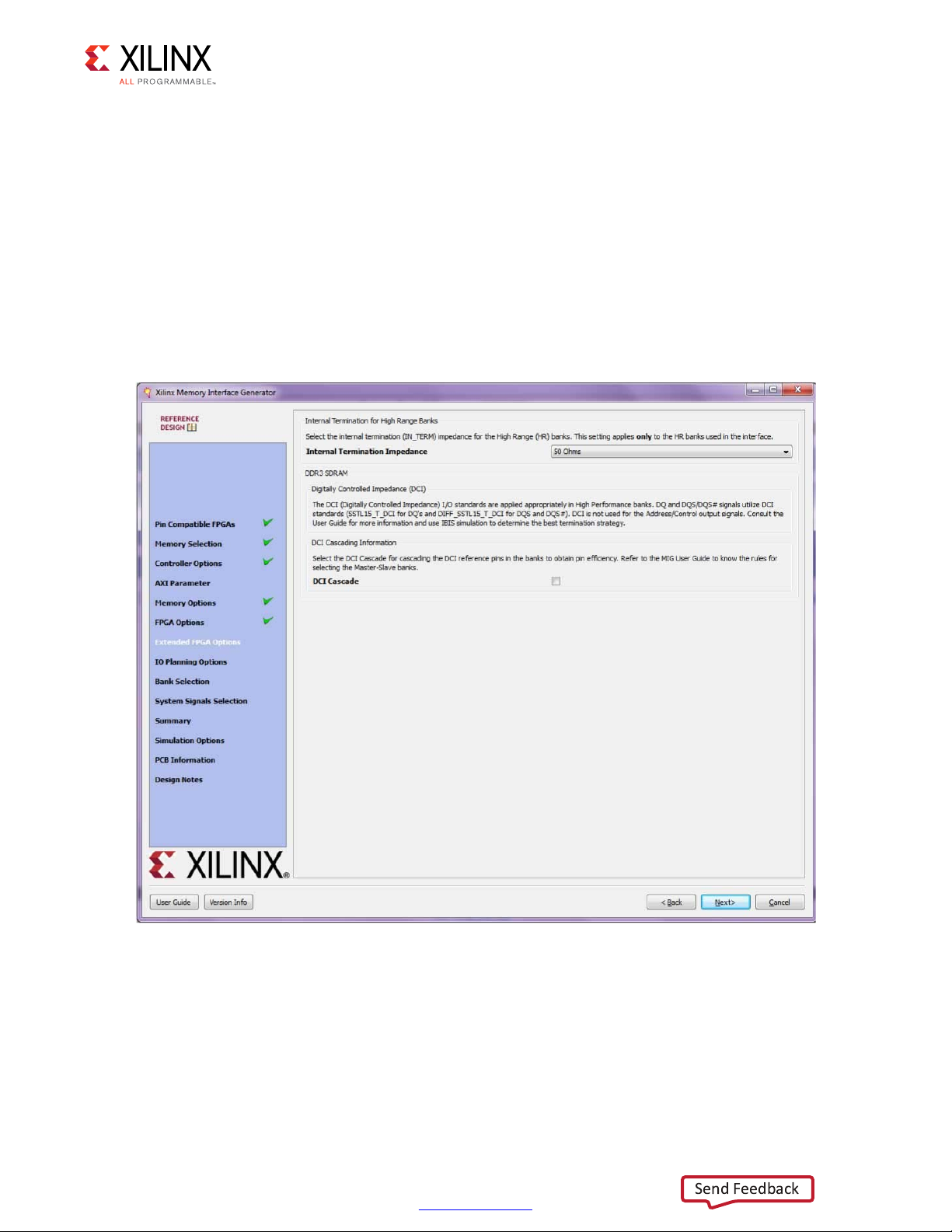
Click Next to display the DCI Description page (Figure 1-23).
Zynq-7000 AP SoC and 7 Series FPGAs MIS v4.1 42
UG586 November 30, 2016
Figure 1-23: DCI Description
• Digitally Controlled Impedance (DCI) – The DCI option allows the use of the FPGA
on-chip internal resistors for termination. DCI must be used for DQ and DQS/DQS#
signals. DCI cascade might have to be used, depending on the pinout and bank
selection. DCI is available in the High Performance Banks.
• Internal Termination for High Range Banks – The internal termination option can be
set to 40, 50, or 60Ω or disabled. This selection is only for High Range banks.
www.xilinx.com
Page 43

X-Ref Target - Figure 1-24
Send Feedback
Chapter 1: DDR3 and DDR2 SDRAM Memory Interface Solution
• DCI Cascade – This selection enables the VRN/VRP pins that are available in High
Performance banks to allocate for the address/control and reset_n ports.
• Pin/Bank Selection Mode – This allows you to specify an existing pinout and generate
the RTL for this pinout, or pick banks for a new design. Figure 1-24 shows the options
for using an existing pinout. You must assign the appropriate pins for each signal. A
choice of each bank is available to narrow down the list of pins. It is not mandatory to
select the banks prior to selection of the pins. Click Validate to check against the MIG
pinout rules. You cannot proceed until the MIG DRC has been validated by clicking
Validate.
Zynq-7000 AP SoC and 7 Series FPGAs MIS v4.1 43
UG586 November 30, 2016
Figure 1-24: Pin/Bank Selection Mode
www.xilinx.com
Page 44

X-Ref Target - Figure 1-25
Send Feedback
Chapter 1: DDR3 and DDR2 SDRAM Memory Interface Solution
Bank Selection
This feature allows the selection of bytes for the memory interface. Bytes can be selected
for different classes of memory signals, such as:
• Address and control signals
• Data signals
Zynq-7000 AP SoC and 7 Series FPGAs MIS v4.1 44
UG586 November 30, 2016
Figure 1-25: Bank Selection
For customized settings, click Deselect Banks and select the appropriate bank and memory
signals. Click Next to move to the next page if the default setting is used.
To unselect the banks that are selected, click Deselect Banks. To restore the defaults, click
Restore Defaults.
VCCAUX_IO groups are shown for HP banks in devices with these groups using dashed lines.
VCCAUX_IO is common to all banks in these groups. The memory interface must have the
same VCCAUX_IO for all banks used in the interface. The MIG core automatically sets the
VCCAUX_IO constraint appropriately for the data rate requested.
www.xilinx.com
Page 45

X-Ref Target - Figure 1-26
Send Feedback
Chapter 1: DDR3 and DDR2 SDRAM Memory Interface Solution
For devices implemented with SSI technology, the SLRs are indicated by a number in the
header in each bank, for example, SLR 1. Interfaces cannot span across Super Logic Regions.
Select the pins for the system signals on this page (Figure 1-26). The MIG tool allows the
selection of either external pins or internal connections, as desired.
Zynq-7000 AP SoC and 7 Series FPGAs MIS v4.1 45
UG586 November 30, 2016
Figure 1-26: System Pins
• sys_clk – This is the system clock input for the memory interface and is typically
connected to a low-jitter external clock source. Either a single input or a differential
pair can be selected based on the System Clock selection in the FPGA Options page
(Figure 1-22). The sys_clk input must be in the same column as the memory
interface. If this pin is connected in the same banks as the memory interface, the MIG
tool selects an I/O standard compatible with the interface, such as DIFF_SSTL15 or
SSTL15. If sys_clk is not connected in a memory interface bank, the MIG tool selects
an appropriate standard such as LVCMOS18 or LVDS. The XDC can be modified as
desired after generation.
www.xilinx.com
Page 46

Chapter 1: DDR3 and DDR2 SDRAM Memory Interface Solution
Send Feedback
• clk_ref – This is the reference frequency input for the IDELAY control. The clk_ref
input can be generated internally or connected to an external source. A single input or
a differential pair can be selected based on the System Clock selection in the FPGA
Options page (Figure 1-22). The I/O standard is selected in a similar way as sys_clk.
• sys_rst – This is the asynchronous system reset input that can be generated internally
or driven from a pin. The MIG tool selects an appropriate I/O standard for the input
such as LVCMOS18 and LVCMOS25 for HP and HR banks, respectively. The default
polarity of sys_rst pin is active-Low. The polarity of sys_rst pin varies based on the
System Reset Polarity option chosen in FPGA Options page (Figure 1-22).
• init_calib_complete – This output indicates that the memory initialization and
calibration is complete and that the interface is ready to use. The
init_calib_complete signal is normally only used internally, but can be brought
out to a pin if desired.
• tg_compare_error – This output indicates that the traffic generator in the example
design has detected a data compare error. This signal is only generated in the example
design and is not part of the user design. This signal is not typically brought out to a
pin but can be, if desired.
Click Next to display the Summary page.
Summary
This page provides the complete details about the 7 series FPGA memory core selection,
interface parameters, IP catalog options, and FPGA options of the active project
(Figure 1-27).
Zynq-7000 AP SoC and 7 Series FPGAs MIS v4.1 46
UG586 November 30, 2016
www.xilinx.com
Page 47

X-Ref Target - Figure 1-27
UG586_c1_38_110610
Send Feedback
Chapter 1: DDR3 and DDR2 SDRAM Memory Interface Solution
Figure 1-27: Summary
Memory Model License
The MIG tool can output a chosen vendor’s memory model for simulation purposes for
memories such as DDR2 or DDR3 SDRAMs. To access the models in the output sim folder,
click the license agreement (Figure 1-28). Read the license agreement and check the Accept
License Agreement box to accept it. If the license agreement is not agreed to, the memory
model is not made available. A memory model is necessary to simulate the design.
Zynq-7000 AP SoC and 7 Series FPGAs MIS v4.1 47
UG586 November 30, 2016
www.xilinx.com
Page 48

X-Ref Target - Figure 1-28
UG586_c1_39_110610
Send Feedback
Chapter 1: DDR3 and DDR2 SDRAM Memory Interface Solution
Figure 1-28: License Agreement
Click Next to move to PCB Information page.
PCB Information
This page displays the PCB-related information to be considered while designing the board
that uses the MIG tool generated designs. Click Next to move to the Design Notes page.
Design Notes
Click Generate to generate the design files. The MIG tool generates two output directories:
example_design and user_design. After generating the design, the MIG GUI closes.
Zynq-7000 AP SoC and 7 Series FPGAs MIS v4.1 48
UG586 November 30, 2016
www.xilinx.com
Page 49

X-Ref Target - Figure 1-29
Send Feedback
Chapter 1: DDR3 and DDR2 SDRAM Memory Interface Solution
Vivado Integrated Design Flow for MIG
1. After clicking Generate, the Generate Output Products window appears. This window
has the Out-of-Context Settings as shown in Figure 1-29.
Figure 1-29: Generate Output Products Window
Zynq-7000 AP SoC and 7 Series FPGAs MIS v4.1 49
UG586 November 30, 2016
www.xilinx.com
Page 50

X-Ref Target - Figure 1-30
Send Feedback
Chapter 1: DDR3 and DDR2 SDRAM Memory Interface Solution
2. Click Out-of-Context Settings to configure generation of synthesized checkpoints. To
enable the Out-of-Context flow, enable the check box. To disable the Out-of-Context
flow, disable the check box. The default option is “enable” as shown in Figure 1-30.
Figure 1-30: Out-of-Context Settings Window
3. MIG core designs comply with “Hierarchical Design" flow in Vivado. For more
information, see the Vivado
Design Suite User Guide: Hierarchical Design (UG905) [Ref 5]
and the Vivado Design Suite Tutorial: Hierarchical Design (UG946) [Ref 6].
Zynq-7000 AP SoC and 7 Series FPGAs MIS v4.1 50
UG586 November 30, 2016
www.xilinx.com
Page 51

X-Ref Target - Figure 1-31
Send Feedback
Chapter 1: DDR3 and DDR2 SDRAM Memory Interface Solution
4. After generating the MIG core design, the project window appears as shown in
Figure 1-31.
Figure 1-31: Vivado Tool Project Window (After IP Generation)
5. After project creation, the XCI file is added to the Project Hierarchy. The same view also
displays the module hierarchies of the user design. The list of HDL and XDC files is
available in the IP Sources view in the Sources window. Double-clicking on any module
or file opens the file in the Vivado Editor. These files are read only.
Zynq-7000 AP SoC and 7 Series FPGAs MIS v4.1 51
UG586 November 30, 2016
www.xilinx.com
Page 52

X-Ref Target - Figure 1-32
Send Feedback
Chapter 1: DDR3 and DDR2 SDRAM Memory Interface Solution
Figure 1-32: Vivado Tool Project Sources Window
Design generation from the MIG tool can be generated using the Create Design flow or
the Verify Pin Changes and Update Design flows. There is no difference between the
flow when generating the design from the MIG tool. Irrespective of the flow by which
designs are generated from the MIG tool, the XCI file is added to the Vivado tool
project. The implementation flow is the same for all scenarios because the flow depends
on the XCI file added to the project.
6. All MIG generated user design RTL and XDC files are automatically added to the project.
If files are modified and you wish to regenerate them, right-click the XCI file and select
Generate Output Products (Figure 1-33).
Zynq-7000 AP SoC and 7 Series FPGAs MIS v4.1 52
UG586 November 30, 2016
www.xilinx.com
Page 53

X-Ref Target - Figure 1-33
Send Feedback
Chapter 1: DDR3 and DDR2 SDRAM Memory Interface Solution
X-Ref Target - Figure 1-34
Figure 1-33: Generate RTL and Constraints
7. Clicking the Generate Output Products option brings up the Manage Outputs window
(Figure 1-34).
Zynq-7000 AP SoC and 7 Series FPGAs MIS v4.1 53
UG586 November 30, 2016
Figure 1-34: Generate Window
www.xilinx.com
Page 54

X-Ref Target - Figure 1-35
Send Feedback
Chapter 1: DDR3 and DDR2 SDRAM Memory Interface Solution
8. All user-design RTL files and constraints files (XDC files) can be viewed in the Sources >
Libraries tab (Figure 1-35).
Figure 1-35: Vivado Project – RTL and Constraints Files
9. The Vivado Design Suite supports Open IP Example Design flow. To create the example
design using this flow right-click the IP in the Source Window, as shown in Figure 1-36
and select.
Zynq-7000 AP SoC and 7 Series FPGAs MIS v4.1 54
UG586 November 30, 2016
www.xilinx.com
Page 55

X-Ref Target - Figure 1-36
Send Feedback
Chapter 1: DDR3 and DDR2 SDRAM Memory Interface Solution
Figure 1-36: Open IP Example Design
10. This option creates a new Vivado project. Selecting the menu brings up a dialog box,
which guides you to the directory for a new design project. Select a directory (or use the
defaults) and click OK.
This launches a new Vivado project with all example design files and a copy of the IP.
This project has example_top as the Implementation top directory, and sim_tb_top
as the Simulation top directory, as shown in Figure 1-37.
Zynq-7000 AP SoC and 7 Series FPGAs MIS v4.1 55
UG586 November 30, 2016
www.xilinx.com
Page 56

X-Ref Target - Figure 1-37
Send Feedback
Chapter 1: DDR3 and DDR2 SDRAM Memory Interface Solution
Figure 1-37: Example Design Project
11. Click Generate Bitstream under Project Manager > Program and Debug to generate
the BIT file for the generated design.
The <project directory>/<project directory>.runs/ impl_1 directory
includes all report files generated for the project after running the implementation. It is
also possible to run the simulation in this project.
12. Recustomization of the MIG IP core can be done by using the Recustomize IP option. It
is not recommended to recustomize the IP in the example_design project. The correct
solution is to close the example_design project, go back to original project and
customize there. Right-click the XCI file and click Recustomize IP (Figure 1-38) to open
the MIG GUI and regenerate the design with the preferred options.
Zynq-7000 AP SoC and 7 Series FPGAs MIS v4.1 56
UG586 November 30, 2016
www.xilinx.com
Page 57

X-Ref Target - Figure 1-38
Send Feedback
Chapter 1: DDR3 and DDR2 SDRAM Memory Interface Solution
Figure 1-38: Recustomize IP
Directory Structure and File Descriptions
Output Directory Structure
The output directory structure of the selected Memo ry Con tr ol ler (M C) de sig n from th e M IG
tool is shown here. In the <component name> directory, three folders are created:
• docs
• example_design
• user_design
Zynq-7000 AP SoC and 7 Series FPGAs MIS v4.1 57
UG586 November 30, 2016
www.xilinx.com
Page 58

mig_7series_v4_1
Send Feedback
docs
example_design
par
rtl
traffic_gen
sim
synth
user_design
rtl
clocking
controller
ip_top
phy
ui
Chapter 1: DDR3 and DDR2 SDRAM Memory Interface Solution
xdc
Directory and File Contents
The 7 series FPGAs core directories and their associated files are listed in this section for
Vivado implementations.
<component name>/example_design/
The example_design folder contains four folders, namely, par, rtl, sim, and synth.
example_design/rtl
This directory contains the example design (Table 1-1).
Table 1-1: Files in example_design/rtl Directory
Name Description
example_top.v/vhd
This top-level module serves as an example for connecting the user
design to the 7 series FPGAs memory interface core.
Zynq-7000 AP SoC and 7 Series FPGAs MIS v4.1 58
UG586 November 30, 2016
www.xilinx.com
Page 59

Chapter 1: DDR3 and DDR2 SDRAM Memory Interface Solution
Send Feedback
example_design/rtl/traffic_gen
This directory contains the traffic generator that provides the stimulus to the
7 series FPGAs Memory Controller (Table 1-2).
Table 1-2: Files in example_design/rtl/traffic_gen Directory
(1)
Name
memc_traffic_gen.v This is the top-level of the traffic generator.
cmd_gen.v
Description
This is the command generator. This module provides
independent control of generating the types of commands,
addresses, and burst lengths.
cmd_prbs_gen.v
memc_flow_vcontrol.v
read_data_path.v This is the top-level for the read datapath.
read_posted_fifo.v
rd_data_gen.v
write_data_path.v This is the top-level for the write datapath.
wr_data_g.v
s7ven_data_gen.v This module generates different data patterns.
a_fifo.v This is a synchronous FIFO using LUT RAMs.
data_prbs_gen.v
init_mem_pattern_ctr.v This module generates flow control logic for the traffic generator.
traffic_gen_top.v
This is a pseudo-random binary sequence (PRBS) generator for
generating PRBS commands, addresses, and burst lengths.
This module generates flow control logic between the Memory
Controller core and the cmd_gen, read_data_path, and
write_data_path modules.
This module stores the read command that is sent to the Memory
Controller, and its FIFO output is used to generate expect data for
read data comparisons.
This module generates timing control for reads and ready signals
to memc_flow_vcontrol.v.
This module generates timing control for writes and ready signals
to memc_flow_vcontrol.v.
This is a 32-bit linear feedback shift register (LFSR) for generating
PRBS data patterns.
This module is the top-level of the traffic generator and comprises
the memc_traffic_gen and init_mem_pattern_ctr modules.
Zynq-7000 AP SoC and 7 Series FPGAs MIS v4.1 59
UG586 November 30, 2016
Notes:
1. All file names are prefixed with the MIG core version number. For example, the MIG 4.1 release module name of
cmd_gen in generated output is now mig_7series_v4_1_cmd_gen.
<component name>/example_design/par
Table 1-3 lists the modules in the example_design/par directory.
Table 1-3: Files in example_design/par Directory
Name Description
example_top.xdc This is the XDC for the core and the example design.
www.xilinx.com
Page 60

Chapter 1: DDR3 and DDR2 SDRAM Memory Interface Solution
Send Feedback
<component name>/example_design/sim
Table 1-4 lists the modules in the example_design/sim directory.
Table 1-4: Files in example_design/sim Directory
Name Description
ddr2_model.v
ddr3_model.v
ddr2_model_parameters.vh
ddr3_model_parameters.vh
ies_run.sh
vcs_run.sh
readme.txt
sim_tb_top.v This is the simulation top file.
Notes:
1. The ies_run.sh and vcs_run.sh files are generated in the folder mig_7series_0_ex/imports when the example design is
created using Open IP Example Design for the design generated with Component Name entered in Vivado IDE as
mig_7series_0.
(1)
(1)
(1)
These are the DDR2 and DDR3 SDRAM models.
These files contain the DDR2 and DDR3 SDRAM model parameter setting.
Linux Executable file for simulating the design using IES simulator.
Linux Executable file for simulating the design using VCS simulator.
Contains the details and prerequisites for simulating the designs using Mentor
Graphics Questa Advanced Simulator, IES, and VCS simulators.
<component name>/user_design
The user_design folder contains the following:
• rtl and xdc folders
• Top-level wrapper module <component_name>.v/vhd
• Top-level modules <component_name>_mig.v/vhd and
<component_name>_mig_sim.v/vhd
The top-level wrapper file <component_name>.v/vhd has an instantiation of top-level
file <component_name>_mig.v/vhd.
Top-level files <component_name>_mig.v/vhd and
<component_name>_mig_sim.v/vhd have the same module name as
<component_name>_mig. These two files are same in all respects except that the file
<component_name>_mig_sim.v/vhd has parameter values set for simulation where
calibration is in fast mode viz., SIM_BYPASS_INIT_CAL = "FAST" etc.
IMPORTANT: The top-level file <component_name>_mig.v/vhd is used for design synthesis and
implementation, whereas the top-level file <component_name>_mig_sim.v/vhd is used in
simulations.
The top-level wrapper file serves as an example for connecting the user_design to the
MIG core.
Zynq-7000 AP SoC and 7 Series FPGAs MIS v4.1 60
UG586 November 30, 2016
www.xilinx.com
Page 61

Chapter 1: DDR3 and DDR2 SDRAM Memory Interface Solution
Send Feedback
user_design/rtl/clocking
This directory contains the user design (Table 1-5).
Table 1-5: Files in user_design/rtl/clocking Directory
(1)
Name
clk_ibuf.v This module instantiates the input clock buffer.
Description
iodelay_ctrl.v
infrastructure.v
Notes:
1. All file names are prefixed with the MIG core version number. For example, for the MIG 4.1 release module name
of clk_ibuf in generated output is now mig_7series_v4_1_clk_ibuf.
This module instantiates IDELAYCNTRL primitives needed for
IDELAY use.
This module helps in clock generation and distribution, and reset
synchronization.
user_design/rtl/controller
This directory contains the Memory Controller that is instantiated in the example design
(Table 1-6).
Table 1-6: Files in user_design/rtl/controller Directory
(1)
Name
arb_mux.v This is the top-level module of arbitration logic.
arb_row_col.v
arb_select.v
bank_cntrl.v
Description
This block receives requests to send row and column commands from the
bank machines and selects one request, if any, for each state.
This module selects a row and column command from the request
information provided by the bank machines.
This structural block instantiates the three subblocks that comprise the
bank machine.
Zynq-7000 AP SoC and 7 Series FPGAs MIS v4.1 61
UG586 November 30, 2016
bank_common.v This module computes various items that cross all of the bank machines.
bank_compare.v This module stores the request for a bank machine.
bank_mach.v This is the top-level bank machine block.
bank_queue.v This is the bank machine queue controller.
bank_state.v This is the primary bank state machine.
col_mach.v This module manages the DQ bus.
mc.v This is the top-level module of the Memory Controller.
mem_intfc.v
rank_cntrl.v This module manages various rank-level timing parameters.
rank_common.v
rank_mach.v This is the top-level rank machine structural block.
This top-level memory interface block instantiates the controller and the
PHY.
This module contains logic common to all rank machines. It contains a
clock prescaler and arbiters for refresh and periodic read.
www.xilinx.com
Page 62

Chapter 1: DDR3 and DDR2 SDRAM Memory Interface Solution
Send Feedback
Table 1-6: Files in user_design/rtl/controller Directory (Cont’d)
(1)
Name
round_robin_arb.v This is a simple round-robin arbiter.
Notes:
1. All file names are prefixed with the MIG core version number. For example, for the MIG 4.1 release module name
of arb_mux in generated output is now mig_7series_v4_1_arb_mux.
Description
user_design/rtl/ip_top
This directory contains the user design (Table 1-7).
Table 1-7: Files in user_design/rtl/ip_top Directory
(1)
Name
Description
mem_intfc.v
memc_ui_top.v This is the top-level Memory Controller module.
Notes:
1. All file names are prefixed with the MIG core version number. For example, for the MIG 4.1 release module name
of mem_intfc in generated output is now mig_7series_v4_1_mem_intfc.
This is the top-level memory interface block that instantiates the
controller and the PHY.
user_design/rtl/phy
This directory contains the 7 series FPGA memory interface PHY implementation
(Table 1-8).
Table 1-8: Files in user_design/rtl/phy Directory
(1)
Name
ddr_byte_group_io
ddr_byte_lane
ddr_calib_top This is the top-level module for the memory physical layer interface.
ddr_if_post_fifo This module extends the depth of a PHASER IN_FIFO up to four entries.
ddr_mc_phy
Description
This module contains the parameterizable I/O logic instantiations and
the I/O terminations for a single byte lane.
This module contains the primitive instantiations required within an
output or input byte lane.
This module is a parameterizable wrapper instantiating up to three I/O
banks, each with 4-lane PHY primitives.
Zynq-7000 AP SoC and 7 Series FPGAs MIS v4.1 62
UG586 November 30, 2016
This wrapper file encompasses the MC_PHY module instantiation and
ddr_mc_phy_wrapper
ddr_of_pre_fifo
ddr_phy_4lanes This module is the parameterizable 4-lane PHY in an I/O bank.
ddr_phy_ck_addr_cmd_delay
ddr_phy_dqs_delay This module contains the DQS to DQ phase offset logic.
handles the vector remapping between the MC_PHY ports and your
DDR2 or DDR3 ports.
This module extends the depth of a PHASER OUT_FIFO up to four
entries.
This module contains the logic to provide the required delay on the
address and control signals.
www.xilinx.com
Page 63
Chapter 1: DDR3 and DDR2 SDRAM Memory Interface Solution
Send Feedback
Table 1-8: Files in user_design/rtl/phy Directory (Cont’d)
(1)
Name
Description
ddr_phy_dqs_found_cal
ddr_phy_init
ddr_phy_rdlvl
ddr_phy_top This is the top-level module for the physical layer.
ddr_phy_wrcal This module contains the write calibration logic.
ddr_phy_wrlvl This module contains the write leveling logic.
ddr_prbs_gen
Notes:
1. All file names are prefixed with the MIG core version number. For example, for the MIG 4.1 release module name
of ddr_byte_group_io in generated output is now mig_7series_v4_1_ddr_byte_group_io.
This module contains the Read leveling calibration logic (PHASER_IN
DQSFOUND calibration logic).
This module contains the memory initialization and overall master
state control during initialization and calibration.
This module contains the Read leveling Stage1 calibration logic
(Window detection with PRBS pattern).
This PRBS module uses a many-to-one feedback mechanism for 2n
sequence generation.
user_design/rtl/ui
This directory contains the user interface code that mediates between the native interface
of the Memory Controller and user applications (Table 1-9).
Table 1-9: Files In user_design/rtl/ui Directory
(1)
Name
Description
ui_cmd.v This is the user interface command port.
ui_rd_data.v
ui_wr_data.v This is the user interface write buffer.
ui_top.v This is the top-level of the Memory Controller user interface.
Notes:
1. All file names are prefixed with the MIG core version number. For example, for the MIG 4.1 release module name
of ui_cmd in generated output is now mig_7series_v4_1_ui_cmd.
This is the user interface read buffer. It reorders read data returned from the
Memory Controller back to the request order.
<component name>/user_design/xdc
Table 1-10 lists the modules in the user_design/xdc directory.
Table 1-10: Files in user_design/xdc Directory
Name Description
<component_name>.xdc This is the XDC for the core and the user design.
Zynq-7000 AP SoC and 7 Series FPGAs MIS v4.1 63
UG586 November 30, 2016
www.xilinx.com
Page 64

Chapter 1: DDR3 and DDR2 SDRAM Memory Interface Solution
Send Feedback
Verify Pin Changes and Update Design
This feature verifies the input XDC for bank selections, byte selections, and pin allocation. It
also generates errors and warnings in a separate dialog box when you click Validate on the
page. This feature is useful to verify the XDC for any pinout changes made after the design
is generated from the MIG tool. You must load the MIG tool generated .prj file, the
original .prj file without any modifications, and the XDC that needs to be verified. In the
Vivado Design Suite, the recustomization option should be selected to reload the project.
The design is allowed to generate only when the MIG DRC is met. Ignore warnings about
validating the pinout, which is the intent. Just validating the XDC is not sufficient; it is
mandatory to proceed with design generation to get the XDC with updated clock and
phaser related constraints and RTL top-level module for various updated Map parameters.
The Update Design feature is required in the following scenarios:
• A pinout is generated using an older version of the MIG tool and the design is to be
revised to the current version of MIG. In MIG, the pinout allocation algorithms have
been changed for certain MIG designs.
• A pinout is generated independent of the MIG tool or is modified after the design is
generated. When a design is generated from the MIG tool, the XDC and HDL code are
generated with the correct constraints.
Here are the rules verified from the input XDC:
• If a pin is allocated to more than one signal, the tool reports an error. Further
verification is not done if the XDC does not adhere to the uniqueness property.
• Verified common rules:
The interface can span across a maximum of three consecutive banks.
°
Interface banks should reside in the same column of the FPGA.
°
Interface banks should be either High Performance (HP) or High Range (HR). HP
°
banks are used for the high frequencies.
The chosen interface banks should have the same SLR region if the chosen device is
°
of stacked silicon interconnect technology.
V
°
I/Os should be used as GPIOs when an internal V
REF
is used or if there are no
REF
inout and input ports in a bank.
The I/O standard of each signal is verified as per the configuration chosen.
°
The VCCAUX I/O of each signal is verified and provides a warning message if the
°
provided VCCAUX I/O is not valid.
• Verified data pin rules:
Zynq-7000 AP SoC and 7 Series FPGAs MIS v4.1 64
UG586 November 30, 2016
Pins related to one strobe set should reside in the same byte group.
°
The strobe pair (DQS) should be allocated to the DQS I/O pair.
°
www.xilinx.com
Page 65

An FPGA byte lane should not contain pins related to two different strobe sets.
Send Feedback
°
V
°
I/O can be used only when the internal V
REF
• Verified address pin rules:
Address signals cannot mix with data bytes except for the ddr3_reset_n signal
°
for DDR3 SDRAM interfaces.
Address signals cannot mix with data bytes except for the ddr2_reset_n signal
°
for DDR2 SDRAM interfaces. The ddr2_reset_n port exists for RDIMMs only.
It can use any number of isolated byte lanes
°
• Verified system pin rules:
System clock:
°
- These pins should be allocated to either SR/MR CC I/O pair.
- These pins must be allocated in the Memory banks column.
- If the selected system clock type is single-ended, you need to check whether the
reference voltage pins are unallocated in the bank or the internal V
Chapter 1: DDR3 and DDR2 SDRAM Memory Interface Solution
is chosen.
REF
is used.
REF
Reference clock:
°
- These pins should be allocated to either SR/MR CC I/O pair.
- If the selected system clock type is single-ended, you need to check whether the
reference voltage pins are unallocated in the bank or the internal V
Status signals:
°
-The sys_rst signal should be allocated in the bank where the V
unallocated or the internal V
- These signals should be allocated in the non-memory banks because the I/O
standard is not compatible. The I/O standard type should be LVCMOS with at
least 1.8V.
- These signals can be allocated in any of the columns (there is no hard
requirement because these signals should reside in a memory column); however,
it is better to allocate closer to the chosen memory banks.
Quick Start Example Design
Overview
is used.
REF
REF
REF
is used.
I/O is
Zynq-7000 AP SoC and 7 Series FPGAs MIS v4.1 65
UG586 November 30, 2016
After the core is successfully generated, the example design HDL can be processed through
the Xilinx implementation toolset.
www.xilinx.com
Page 66

X-Ref Target - Figure 1-39
UG586_c1_41_120311
ddr2_sim_tb_top or ddr3_sim_tb_top
Example Design
app_addr
app_cmd
app_en
app_hi_pri
app_wdf_data
app_wdf_end
app_wdf_mask
app_wdf_wren
app_rd_data
app_rd_data_end
app_rd_data_valid
app_wdf_rdy
traffic_gen_top
memc_ui_top
ui_top mem_Intfc
DDR2/DDR3
SDRAM
cmd
accept
use_addr
bank_mach_next
data_buf_addr
wr_data_en
wr_data_addr
wr_data_en
wr_data_be
rd_data_en
rd_data
MC
phy_top
error
Parameter:
BEGIN_ADDR
END_ADDR
nCK_PER_CLK
iodelayctrl infrastructure
app_rdy
user_design_top Wrapper
user_design_top
Send Feedback
Chapter 1: DDR3 and DDR2 SDRAM Memory Interface Solution
Implementing the Example Design
For more information on using an IP example design, see the Vivado Design Suite User
Guide: Designing with IP (UG896) [Ref 7].
Simulating the Example Design (for Designs with the Standard User Interface)
The MIG tool provides a synthesizable test bench to generate various traffic data patterns
to the Memory Controller (MC). This test bench consists of a memc_ui_top wrapper, a
traffic_generator that generates traffic patterns through the user interface to a
ui_top core, and an infrastructure core that provides clock resources to the memc_ui_top
core. A block diagram of the example design test bench is shown in Figure 1-39.
Figure 1-40 shows the simulation result of a simple read and write transaction between the
tb_top and memc_intfc modules.
Zynq-7000 AP SoC and 7 Series FPGAs MIS v4.1 66
UG586 November 30, 2016
Figure 1-39: Synthesizable Example Design Block Diagram
www.xilinx.com
Page 67

X-Ref Target - Figure 1-40
Read command to 0xd00
is accepted here
Memory User interface asserts
app_rd_data_valid signal to
indicate valid data (0x...0d00)
returning from memory.
Address as data(0x...0e00) value are written
to data fifo when app_wdf_wren and the
app_wdf_end are asserted. A Write
command to 0xe00 is accepted here.
Send Feedback
Chapter 1: DDR3 and DDR2 SDRAM Memory Interface Solution
Figure 1-40: User Interface Read and Write Cycle
Traffic Generator Operation
The traffic generator module contained within the synthesizable test bench can be
parameterized to create various stimulus patterns for the memory design. It can produce
repetitive test patterns for verifying design integrity as well as pseudo-random data
streams that model real-world traffic.
You can define the address range through the BEGIN_ADDRESS and END_ADDRESS
parameters. The Init Memory Pattern Control block directs the traffic generator to step
sequentially through all the addresses in the address space, writing the appropriate data
value to each location in the memory device as determined by the selected data pattern. By
default, the test bench uses the address as the data pattern, but the data pattern in this
example design can be modified using vio_data_mode signals that can be modified
within the Vivado logic analyzer feature.
When the memory has been initialized, the traffic generator begins stimulating the user
interface port to create traffic to and from the memory device. By default, the traffic
generator sends pseudo-random commands to the port, meaning that the instruction
sequences (R/W, R, W) and addresses are determined by PRBS generator logic in the traffic
generator module.
Zynq-7000 AP SoC and 7 Series FPGAs MIS v4.1 67
UG586 November 30, 2016
www.xilinx.com
Page 68

Chapter 1: DDR3 and DDR2 SDRAM Memory Interface Solution
Send Feedback
The read data returning from the memory device is accessed by the traffic generator
through the user interface read data port and compared against internally generated
“expect” data. If an error is detected (that is, there is a mismatch between the read data and
expected data), an error signal is asserted and the readback address, readback data, and
expect data are latched into the error_status outputs.
Modifying the Example Design
The provided example_top design comprises traffic generator modules and can be
modified to tailor different command and data patterns. A few high-level parameters can
be modified in the example_top.v/vhd module. Table 1-11 describes these parameters.
Table 1-11: Traffic Generator Parameters Set in the example_top Module
Parameter Description Value
FAMILY Indicates the family type. “VIRTEX7”
MEMORY_TYPE
nCK_PER_CLK
NUM_DQ_PINS
MEM_BURST_LEN
MEM_COL_WIDTH
DATA_WIDTH
ADDR_WIDTH
MASK_SIZE
PORT_MODE Sets the port mode.
Indicate the Memory Controller
type.
This is the Memory Controller clock
to DRAM clock ratio.
The is the total memory DQ bus
width.
This is the memory data burst
length.
This is the number of memory
column address bits.
This is the user interface data bus
width.
This is the memory address bus
width. It is equal to RANK_WIDTH +
BANK_WIDTH + ROW_WIDTH +
COL_WIDTH.
This parameter specifies the mask
width in the user interface data bus.
“DDR2”, “DDR3”
4, 2 (depends on the PHY to Controller Clock
ratio chosen in the GUI)
This parameter supports DQ widths from 8
to a maximum of 72 in increments of 8. The
available maximum DQ width is frequency
dependent on the selected memory device.
This must be set to 8.
This option is based on the selected
memory device.
For nCK_PER_CLK = 4,
DATA_WIDTH = NUM_DQ_PINS × 8.
BI_MODE: Generate a WRITE data pattern
and monitor the READ data for comparison.
BEGIN_ADDRESS
END_ADDRESS
Zynq-7000 AP SoC and 7 Series FPGAs MIS v4.1 68
UG586 November 30, 2016
Sets the memory start address
boundary.
Sets the memory end address
boundary.
www.xilinx.com
This parameter defines the start boundary
for the port address space. The
least-significant Bits[3:0] of this value are
ignored.
This parameter defines the end boundary
for the port address space. The
least-significant Bits[3:0] of this value are
ignored.
Page 69

Chapter 1: DDR3 and DDR2 SDRAM Memory Interface Solution
Send Feedback
Table 1-11: Traffic Generator Parameters Set in the example_top Module (Cont’d)
Parameter Description Value
This parameter is used with the PRBS
address generator to shift random
PRBS_EADDR_MASK_POS Sets the 32-bit AND MASK position.
PRBS_SADDR_MASK_POS Sets the 32-bit OR MASK position.
This parameter sets the command
pattern circuits to be generated. For
a larger device, the CMD_PATTERN
can be set to “CGEN_ALL.” This
CMD_PATTERN
parameter enables all supported
command pattern circuits to be
generated. However, it is sometimes
necessary to limit a specific
command pattern because of
limited resources in a smaller device.
addresses down into the port address space.
The END_ADDRESS value is ANDed with the
PRBS address for bit positions that have a 1
in this mask.
This parameter is used with the PRBS
address generator to shift random
addresses up into the port address space.
The START_ADDRESS value is ORed with the
PRBS address for bit positions that have a 1
in this mask
Valid settings for this signal are:
• CGEN_FIXED: The address, burst length,
and instruction are taken directly from the
fixed_addr_i, fixed_bl_i, and fixed_instr_i
inputs.
• CGEN_SEQUENTIAL: The address is
increased sequentially, and the increment
is determined by the data port size.
• CGEN_PRBS: A 32-stage Linear Feedback
Shift register (LFSR) generates
pseudo-random addresses, burst lengths,
and instruction sequences. The seed can
be set from the 32-bit cmd_seed input.
• CGEN_ALL (default): This option turns on
all of the options above and allows
addr_mode_i, instr_mode_i, and
bl_mode_i to select the type of generation
during run time.
Zynq-7000 AP SoC and 7 Series FPGAs MIS v4.1 69
UG586 November 30, 2016
www.xilinx.com
Page 70

Chapter 1: DDR3 and DDR2 SDRAM Memory Interface Solution
Send Feedback
Table 1-11: Traffic Generator Parameters Set in the example_top Module (Cont’d)
Parameter Description Value
Valid settings for this parameter are:
• ADDR (default): The address is used as a
data pattern.
• HAMMER: All 1s are on the DQ pins
during the rising edge of DQS, and all 0s
are on the DQ pins during the falling edge
of DQS.
• WALKING1: Walking 1s are on the DQ pins
and the starting position of 1 depends on
the address value.
• WALKING0: Walking 0s are on the DQ pins
and the starting position of 0 depends on
the address value.
DATA_PATTERN
This parameter sets the data pattern
circuits to be generated through RTL
logic. For larger devices, the
DATA_PATTERN can be set to
“DGEN_ALL,” enabling all supported
data pattern circuits to be
generated. In hardware, the data
pattern is selected and/or changed
using vio_data_value_mode. The
pattern can only be changed when
DATA_PATTERN is set to DGEN_ALL.
• NEIGHBOR: The Hammer pattern is on all
DQ pins except one. The address
determines the exception pin location.
• PRBS: A 32-stage LFSR generates random
data and is seeded by the starting
address.
• DGEN_ALL: This option turns on all
available options:
0x1: FIXED – 32 bits of fixed_data.
0x2: ADDRESS – 32 bits address as data.
0x3: HAMMER
0x4: SIMPLE8 – Simple eight data pattern
that repeats every eight words.
0x5: WALKING1s – Walking 1s are on the
DQ pins.
0x6: WALKING0s – Walking 0s are on the
DQ pins.
0x7: PRBS – A 32-stage LFSR generates
random data.
0x9: SLOW HAMMER – This is the slow
MHz hammer data pattern.
0xA: PHY_CALIB pattern – 0xFF, 00, AA, 55,
55, AA, 99, 66. This mode only generates
READ commands at address zero.
CMDS_GAP_DELAY
SEL_VICTIM_LINE
Zynq-7000 AP SoC and 7 Series FPGAs MIS v4.1 70
UG586 November 30, 2016
This parameter allows pause delay
between each user burst command.
Select a victim DQ line whose state
is always at logic High.
www.xilinx.com
Valid values: 0 to 32.
This parameter only applies to the Hammer
pattern. Valid settings for this parameter are
0 to NUM_DQ_PINS.
When value = NUM_DQ_PINS, all DQ pins
have the same Hammer pattern.
Page 71

Chapter 1: DDR3 and DDR2 SDRAM Memory Interface Solution
Send Feedback
Table 1-11: Traffic Generator Parameters Set in the example_top Module (Cont’d)
Parameter Description Value
Force the traffic generator to only
EYE_TEST
Notes:
1. The traffic generator might support more options than are available in the 7 series Memory Controller. The settings must
match supported values in the Memory Controller.
generate writes to a single location,
and no read transactions are
generated.
Valid settings for this parameter are “TRUE”
and “FALSE.”
When set to “TRUE,” any settings in
vio_instr_mode_value are overridden.
The command patterns instr_mode_i, addr_mode_i, bl_mode_i, and data_mode_i
of the traffic_gen module can each be set independently. The provided
init_mem_pattern_ctr module has interface signals that allow you to modify the
command pattern in real-time using the Vivado debug logic core virtual I/O (VIO).
This is the varying command pattern:
1. Set vio_modify_enable to 1.
2. Set vio_addr_mode_value to:
1: Fixed_address.
2: PRBS address.
3: Sequential address.
3. Set vio_bl_mode_value to:
1: Fixed bl.
2: PRBS bl. If bl_mode value is set to 2, the addr_mode value is forced to 2 to generate
the PRBS address.
4. Set vio_data_mode_value to:
0: Reserved.
1: FIXED data mode. Data comes from the fixed_data_i input bus.
2: DGEN_ADDR (default). The address is used as the data pattern.
3: DGEN_HAMMER. All 1s are on the DQ pins during the rising edge of DQS, and all 0s are
on the DQ pins during the falling edge of DQS.
4: DGEN_NEIGHBOR. All 1s are on the DQ pins during the rising edge of DQS except one
pin. The address determines the exception pin location.
Zynq-7000 AP SoC and 7 Series FPGAs MIS v4.1 71
UG586 November 30, 2016
www.xilinx.com
Page 72

Chapter 1: DDR3 and DDR2 SDRAM Memory Interface Solution
Send Feedback
5: DGEN_WALKING1. Walking 1s are on the DQ pins. The starting position of 1 depends
on the address value.
6: DGEN_WALKING0. Walking 0s are on the DQ pins. The starting position of 0 depends
on the address value.
7: DGEN_PRBS. A 32-stage LFSR generates random data and is seeded by the starting
address. This data mode only works with PRBS address mode or Sequential address
mode.
Modifying Port Address Space
The address space for a port can be modified by changing the BEGIN_ADDRESS and
END_ADDRESS parameters found in the top-level test bench file. These two values must be
set to align to the port data width. The two additional parameters, PRBS_SADDR_MASK_POS
and PRBS_EADDR_MASK_POS, are used in the default PRBS address mode to ensure that
out-of-range addresses are not sent to the port. PRBS_SADDR_MASK_POS creates an OR
mask that shifts PRBS-generated addresses with values below BEGIN_ADDRESS up into the
valid address space of the port. PRBS_SADDR_MASK_POS should be set to a 32-bit value
equal to the BEGIN_ADDRESS parameter. PRBS_EADDR_MASK_POS creates an AND mask
that shifts PRBS-generated addresses with values above END_ADDRESS down into the valid
address space of the port. PRBS_EADDR_MASK_POS should be set to a 32-bit value, where
all bits above the most-significant address bit of END_ADDRESS are set to 1 and all
remaining bits are set to 0. Table 1-12 shows some examples of setting the two mask
parameters.
Table 1-12: Example Settings for Address Space and PRBS Masks
SADDR EADDR PRBS_SADDR_MASK_POS PRBS_EADDR_MASK_POS
0x1000 0xFFFF 0x00001000 0xFFFF0000
0x2000 0xFFFF 0x00002000 0xFFFF0000
0x3000 0xFFFF 0x00003000 0xFFFF0000
0x4000 0xFFFF 0x00004000 0xFFFF0000
0x5000 0xFFFF 0x00005000 0xFFFF0000
0x2000 0x1FFF 0x00002000 0xFFFFE000
0x2000 0x2FFF 0x00002000 0xFFFFD000
0x2000 0x3FFF 0x00002000 0xFFFFC000
0x2000 0x4FFF 0x00002000 0xFFFF8000
0x2000 0x5FFF 0x00002000 0xFFFF8000
0x2000 0x6FFF 0x00002000 0xFFFF8000
0x2000 0x7FFF 0x00002000 0xFFFF8000
0x2000 0x8FFF 0x00002000 0xFFFF0000
0x2000 0x9FFF 0x00002000 0xFFFF0000
Zynq-7000 AP SoC and 7 Series FPGAs MIS v4.1 72
UG586 November 30, 2016
www.xilinx.com
Page 73

Chapter 1: DDR3 and DDR2 SDRAM Memory Interface Solution
Send Feedback
Table 1-12: Example Settings for Address Space and PRBS Masks (Cont’d)
SADDR EADDR PRBS_SADDR_MASK_POS PRBS_EADDR_MASK_POS
0x2000 0xAFFF 0x00002000 0xFFFF0000
0x2000 0xBFFF 0x00002000 0xFFFF0000
0x2000 0xCFFF 0x00002000 0xFFFF0000
0x2000 0xDFFF 0x00002000 0xFFFF0000
0x2000 0xEFFF 0x00002000 0xFFFF0000
0x2000 0xFFFF 0x00002000 0xFFFF0000
Traffic Generator Signal Description
Traffic generator signals are described in Table 1-13.
Table 1-13: Traffic Generator Signal Descriptions
Signal Direction Description
clk_i Input This signal is the clock input.
memc_init_done Input
manual_clear_error Input Input signal to clear error flag.
memc_cmd_addr_o[31:0] Output Start address for current transaction.
memc_cmd_en_o Output
memc_cmd_full_i Input
memc_cmd_instr[2:0] Output
memc_rd_data_i[DWIDTH – 1:0] Input Read data value returning from memory.
memc_rd_empty_i Input
memc_rd_en_o Output This signal is only used in MCB-like interface.
memc_wr_data_o[DWIDTH –
1:0]
memc_wr_en_o Output
Output
This is the input status signal from the Memory Controller to
indicate that it is ready accept traffic.
This active-High signal is the write-enable signal for the Command
FIFO.
This connects to inversion of app_rdy of Memory Controller. When
this input signal is asserted, TG continues to assert the
memc_cmd_en_o, memc_cmd_addr_o value and memc_cmd_instr
until the memc_cmd_full_i is deasserted.
Command code for current instruction.
Command Write: 3'b000
Command Read: 3'b001
This active-High signal is the empty flag for the Read Data FIFO in
Memory Controller. It indicates there is no valid data in the FIFO.
Write data value to be loaded into Write Data FIFO in Memory
Controller.
This active-High signal is the write enable for the Write Data FIFO.
It indicates that the value on memc_wr_data is valid.
memc_wr_full_i Input
qdr_wr_cmd_o Output
Zynq-7000 AP SoC and 7 Series FPGAs MIS v4.1 73
UG586 November 30, 2016
This active-High signal is the full flag for the Write Data FIFO from
Memory Controller. When this signal is High, TG holds the write
data value and keeps assertion of memc_wr_en until the
memc_wr_full_i goes Low.
This signal is only used to send write commands to the QDR II+
user interface.
www.xilinx.com
Page 74

Chapter 1: DDR3 and DDR2 SDRAM Memory Interface Solution
Send Feedback
Table 1-13: Traffic Generator Signal Descriptions (Cont’d)
Signal Direction Description
vio_modify_enable Input Allow vio_xxxx_mode_value to alter traffic pattern.
Valid settings for this signal are:
•0x0: Reserved.
• 0x1: FIXED – 32 bits of fixed_data as defined through
fixed_data_i inputs.
• 0x2: ADDRESS – 32 bits address as data. Data is generated based
on the logical address space. If a design has a 256-bit user data
bus, each write beat in the user bus would have a 256/8 address
increment in byte boundary. If the starting address is 1,300, the
data is 1,300, followed by 1,320 in the next cycle. To simplify the
logic, the user data pattern is a repeat of the increment of the
address value Bits[31:0].
• 0x3: HAMMER – All 1s are on DQ pins during the rising edge of
DQS, and all 0s are on the DQ pins during the falling edge of
DQS, except the VICTIM line as defined in the parameter
“SEL_VICTIM_LINE.” This option is only valid if parameter
DATA_PATTERN = “DGEN_HAMMER” or “DGEN_ALL.”
vio_data_mode_value[3:0] Input
• 0x4: SIMPLE8 – Simple 8 data pattern that repeats every 8 words.
The patterns can be defined by the “simple_datax” inputs.
• 0x5: WALKING1s – Walking 1s are on the DQ pins. The starting
position of 1 depends on the address value. This option is only
valid if the parameter DATA_PATTERN = “DGEN_WALKING” or
“DGEN_ALL.”
• 0x6: WALKING0s – Walking 0s are on the DQ pins. The starting
position of 0 depends on the address value. This option is only
valid if the parameter DATA_PATTERN = “DGEN_WALKING0” or
“DGEN_ALL.”
• 0x7: PRBS – A 32-stage LFSR generates random data and is
seeded by the starting address. This option is only valid if the
parameter DATA_PATTERN = “DGEN_PRBS” or “DGEN_ALL.”
• 0x9: SLOW HAMMER – This is the slow MHz hammer data
pattern.
• 0xA: PHY_CALIB pattern – 0xFF, 00, AA, 55, 55, AA, 99, 66. This
mode only generates READ commands at address zero. This is
only valid in the Virtex
®
-7 family.
vio_addr_mode_value[2:0] Input
Zynq-7000 AP SoC and 7 Series FPGAs MIS v4.1 74
UG586 November 30, 2016
Valid settings for this signal are:
• 0x1: FIXED address mode. The address comes from the
fixed_addr_i input bus. With FIXED address mode, the
data_mode is limited to the fixed_data_input. No PRBS data
pattern is generated.
• 0x2: PRBS address mode (Default). The address is generated
from the internal 32-bit LFSR circuit. The seed can be changed
through the cmd_seed input bus.
• 0x3: SEQUENTIAL address mode. The address is generated from
the internal address counter. The increment is determined by the
user interface port width.
www.xilinx.com
Page 75

Chapter 1: DDR3 and DDR2 SDRAM Memory Interface Solution
Send Feedback
Table 1-13: Traffic Generator Signal Descriptions (Cont’d)
Signal Direction Description
Valid settings for this signal are:
• 0x1: Command type (read/write) as defined by fixed_instr_i.
vio_instr_mode_value[3:0] Input
vio_bl_mode_value[3:0] Input
vio_fixed_instr_value Input
vio_fixed_bl_value Input Valid settings are 1 to 256.
• 0x2: Random read/write commands.
• 0xE: Write only at address zero.
• 0xF: Read only at address zero.
Valid settings for this signal are:
• 0x1: Fixed burst length as defined in the fixed_bl_i inputs.
• 0x2: The user burst length is generated from the internal PRBS
generator. Each burst value defines the number of back-to-back
commands that are generated.
Valid settings are:
• 0x0: Write instruction
• 0x1: Read instruction
vio_pause_traffic Input Pause traffic generation on-the-fly.
This mode is only used if the data mode pattern is address as data.
If this is enabled, a random memc_wr_mask is generated after the
vio_data_mask_gen Input
cmp_data[DWIDTH – 1:0] Output Expected data to be compared with read back data from memory.
cmp_data_valid Output Compare data valid signal.
cmp_error Output
error Output
error_status[n:0] Output
memory pattern has been filled in memory. The write data byte
lane is jammed with 8'hFF if the corresponding memc_write_mask
is asserted.
This compare error flag asserts whenever cmp_data is not the same
as the readback data from memory.
This signal is asserted when the readback data is not equal to the
expected value.
This signal latches these values when the error signal is asserted:
• [31:0]: Read start address
• [37:32]: Read burst length
• [39:38]: Reserved
• [40]: mcb_cmd_full
• [41]: mcb_wr_full
• [42]: mcb_rd_empty
• [64 + (DWIDTH – 1):64]: expected_cmp_data
• [64 + (2 × DWIDTH – 1):64 + DWIDTH]: read_data
simple_data0[31:0] Input User-defined simple data 0 for simple 8 repeat data pattern.
simple_data1[31:0] Input User-defined simple data 1 for simple 8 repeat data pattern.
simple_data2[31:0] Input User-defined simple data 2 for simple 8 repeat data pattern.
simple_data3[31:0] Input User-defined simple data 3 for simple 8 repeat data pattern.
Zynq-7000 AP SoC and 7 Series FPGAs MIS v4.1 75
UG586 November 30, 2016
www.xilinx.com
Page 76

Chapter 1: DDR3 and DDR2 SDRAM Memory Interface Solution
Send Feedback
Table 1-13: Traffic Generator Signal Descriptions (Cont’d)
Signal Direction Description
simple_data4[31:0] Input User-defined simple data 4 for simple 8 repeat data pattern.
simple_data5[31:0] Input User-defined simple data 5 for simple 8 repeat data pattern.
simple_data6[31:0] Input User-defined simple data 6 for simple 8 repeat data pattern.
simple_data7[31:0] Input User-defined simple data 7 for simple 8 repeat data pattern.
fixed_data_i[31:0] Input User-defined fixed data pattern.
User-defined fixed command pattern.
fixed_instr_i[2:0] Input
000: Write command
001: Read command
fixed_bl_i[5:0] Input
Memory Initialization and Traffic Test Flow
After power-up, the Init Memory Control block directs the traffic generator to initialize the
memory with the selected data pattern through the memory initialization procedure.
Memory Initialization
1. The data_mode_i input is set to select the data pattern (for example,
data_mode_i[3:0] = 0010 for the address as the data pattern).
2. The start_addr_i input is set to define the lower address boundary.
3. The end_addr_i input is set to define the upper address boundary.
4. The bl_mode_i is set to 01 to get the burst length from the fixed_bl_i input.
5. The fixed_bl_i input is set to either 16 or 32.
6. The instr_mode_i is set to 0001 to get the instruction from the fixed_instr_i
input.
7. The fixed_instr_i input is set to the “WR” command value of the memory device.
User-defined fixed burst length. Each burst value defines the
number of back to back commands that are generated.
Zynq-7000 AP SoC and 7 Series FPGAs MIS v4.1 76
UG586 November 30, 2016
8. The addr_mode_i is set to 11 for the sequential address mode to fill up the memory
space.
9. The mode_load_i is asserted for one clock cycle.
When the memory space is initialized with the selected data pattern, the Init Memory
Control block instructs the traffic generator to begin running traffic through the traffic test
flow procedure (by default, the addr_mode_i, instr_mode_i, and bl_mode_i inputs
are set to select PRBS mode).
Traffic Test Flow
1. The addr_mode_i input is set to the desired mode (PRBS is the default).
www.xilinx.com
Page 77

Chapter 1: DDR3 and DDR2 SDRAM Memory Interface Solution
Send Feedback
2. The cmd_seed_i and data_seed_i input values are set for the internal PRBS
generator. This step is not required for other patterns.
3. The instr_mode_i input is set to the desired mode (PRBS is the default).
4. The bl_mode_i input is set to the desired mode (PRBS is the default).
5. The data_mode_i input should have the same value as in the memory pattern
initialization stage detailed in Memory Initialization.
6. The run_traffic_i input is asserted to start running traffic.
7. If an error occurs during testing (for example, the read data does not match the
expected data), the error bit is set until reset is applied.
8. Upon receiving an error, the error_status bus latches the values defined in Table 1-13,
page 73.
With some modifications, the example design can be changed to allow addr_mode_i,
instr_mode_i, and bl_mode_i to be changed dynamically when run_traffic_i is
deasserted. However, after changing the setting, the memory initialization steps need to be
repeated to ensure that the proper pattern is loaded into the memory space.
Note:
When the chip select option is disabled, the simulation test bench always ties the
°
memory model chip select bit(s) to zero for proper operation.
When the data mask option is disabled, the simulation test bench always ties the
°
memory model data mask bit(s) to zero for proper operation.
Simulating the Example Design (for Designs with the AXI4 Interface)
The MIG tool provides a synthesizable AXI4 test bench to generate various traffic patterns
to the Memory Controller. This test bench consists of an instance of user design (Memory
Controller) with AXI4 interface, a traffic_generator (axi4_tg) that generates traffic patterns
through the AXI4 interface of the controller as shown in Figure 1-41. The infrastructure
block inside the user design provides clock resources to both the controller and the traffic
generator. Figure 1-41 shows a block diagram of the example design test bench. The details
of the clocks in Figure 1-41 are provided in Clocking Architecture, page 119.
Zynq-7000 AP SoC and 7 Series FPGAs MIS v4.1 77
UG586 November 30, 2016
www.xilinx.com
Page 78

X-Ref Target - Figure 1-41
$$2X
-EMORY
AXI?TG
MEMC ?UI ?TOP ?AXI
#ONTROLLERWITH
!8)INTERFACE
0(9
INFRASTRUCTURE
53%2?$%3)'.COMPONENT
MIG ?SERIES ?VX?X
SYS ?CLK ?P
SYS ?CLK ?N
CLK ?IBUF
!8)$ATAAND#ONTROL0ORTS
!8)
7RAPPER
4RAFFIC
'ENERATOR
IODELAY ?
CTRL
CLK ?REF ?N
CLK ?REF ?P
SYS ?RST
CLK ?REF )$%,!9#42,
IODELAY ?CTRL ?RDY
SYS ?RST
MMCM ?CLK
RST
CLK &ABRIC 0(9LOGIC
MEM?REFCLK
FREQ ?REFCLK
RST ?PHASSR ?REF
SYNC ?PULSE
PLL ?LOCKED
REF?DLL ?LOCK
INIT ?CALIB ?COMPLETE
UI?CLK
ARESETN
!8)234
,OGIC
UI?CLK ?SYNC ?RST
8
Send Feedback
Chapter 1: DDR3 and DDR2 SDRAM Memory Interface Solution
X-Ref Target - Figure 1-42
Figure 1-41: Synthesizable Example Design Block for AXI4 Interface
Figure 1-42 shows the simple write transaction being performed on the AXI4 interface. This
transaction consists of a command phase, a data phase, and a response phase. This follows
the standard AXI4 protocol.
Figure 1-42: AXI4 Interface Write Cycle
Zynq-7000 AP SoC and 7 Series FPGAs MIS v4.1 78
UG586 November 30, 2016
www.xilinx.com
Page 79

X-Ref Target - Figure 1-43
Send Feedback
Chapter 1: DDR3 and DDR2 SDRAM Memory Interface Solution
Figure 1-43 shows a simple read transaction being performed on the AXI4 interface. This
transaction consists of a command phase and data phase. This follows the standard AXI4
protocol.
Figure 1-43: AXI4 Interface Read Cycle
The example design generated when the AXI4 interface is selected as the user interface is
different compared to the standard traffic generator user interface. The intent of this
synthesizable test bench is to verify the basic AXI4 transactions as well as the Memory
Controller transactions. However, this test bench does not verify all Memory Controller
features and is aimed at verifying the AXI4 SHIM features. Table 1-14 shows the signals of
interest during verification of the AXI4 test bench. These signals can be found in the
example_top module.
Table 1-14: Signals of Interest During Simulation for the AXI4 Test Bench
Signal Description
test_cmptd
write_cmptd
cmd_err
write_err
dbg_wr_sts_vld
dbg_wr_sts
read_cmptd
read_err
When asserted, this signal indicates that the current round of tests with random
reads and writes is completed. This signal is deasserted when a new test starts.
This signal is asserted for one clock indicating that the current write transaction is
completed.
When asserted, this signal indicates that the command phase of the AXI4 transaction
(read or write) has an error.
When asserted, this signal indicates that the write transaction to memory resulted in
an error.
When asserted, this signal indicates a valid status for the write transaction on the
dbg_wr_sts bus. This signal is asserted even if the write transaction does not
complete.
This signal has the status of the write transaction. The details of the status are given
in Table 1-15.
This signal is asserted for one clock indicating that the current read transaction is
completed.
When asserted, this signal indicates that the read transaction to the memory resulted
in an error.
Zynq-7000 AP SoC and 7 Series FPGAs MIS v4.1 79
UG586 November 30, 2016
www.xilinx.com
Page 80

Chapter 1: DDR3 and DDR2 SDRAM Memory Interface Solution
Send Feedback
Table 1-14: Signals of Interest During Simulation for the AXI4 Test Bench
Signal Description
When asserted, this signal indicates a valid status for the read transaction on the
dbg_rd_sts_vld
dbg_rd_sts bus. This signal is asserted even if the read transaction does not
complete.
X-Ref Target - Figure 1-44
dbg_rd_sts
This signal has the status of the read transaction. The details of the status are given
in Table 1-16.
The initialization and the calibration sequence remain the same as that indicated in
Simulating the Example Design (for Designs with the Standard User Interface), page 66. The
status that is generated for a write transaction can be found in Figure 1-44.
Figure 1-44: Status for the Write Transaction
Table 1-15: Debug Status for the Write Transaction
Bits Description
39:32 Number of beats/write transfers completed for last burst
31:21 Reserved
Data pattern used for the current transaction:
• 000: 5A and A5
• 001: PRBS pattern
20:18
17 Write error occurred. The write transaction could not be completed.
16 Command error occurred during a write transaction.
15:9 Reserved
8:6
• 010: Walking zeros
• 011: Walking ones
• 100: All ones
• 101: All zeros
AXI wrapper write FSM state when timeout (watchdog timer should be enabled) occurs:
• 3'b001: Data write transaction
• 3'b010: Waiting for acknowledgment for written data
• 3'b011: Dummy data write transaction
• 3'b100: Waiting for response from the response channel
Zynq-7000 AP SoC and 7 Series FPGAs MIS v4.1 80
UG586 November 30, 2016
www.xilinx.com
Page 81

X-Ref Target - Figure 1-45
Send Feedback
Chapter 1: DDR3 and DDR2 SDRAM Memory Interface Solution
Table 1-15: Debug Status for the Write Transaction (Cont’d)
Bits Description
5:2 Response ID for the write response
1:0 Write response received for AXI
The status generated for a read transaction is shown in Figure 1-45.
Figure 1-45: Status for the Read Transaction
Table 1-16: Debug Status for the Read Transaction
Bits Description
39:32 Number of beats/read transfers completed for last burst
31:30 Reserved
Data pattern used for the current check:
• 000: 5A and A5
• 001: PRBS pattern
29:27
26:19 Pointer value for which the mismatch occurred
18 Data mismatch occurred between the written data and read data
17 Read error occurred, read transaction could not be completed
16 Command error occurred during read transaction
15:4 Reserved
• 010: Walking zeros
• 011: Walking ones
• 100: All ones
• 101: All zeros
Zynq-7000 AP SoC and 7 Series FPGAs MIS v4.1 81
UG586 November 30, 2016
AXI wrapper read FSM state when timeout (watchdog timer should be enabled) occurs:
3:2
1 Incorrect response ID presented by the AXI slave
0 Read error response on AXI
• 2'b01: Read command transaction
• 2'b10: Data read transaction
www.xilinx.com
Page 82

Chapter 1: DDR3 and DDR2 SDRAM Memory Interface Solution
Send Feedback
Calibration and other DDR data read and write transactions are similar to what is described
in Simulating the Example Design (for Designs with the Standard User Interface), page 66.
The AXI4 write and read transactions are started only after the init_calib_complete
signal is asserted.
Setting Up for Simulation
IMPORTANT: The Xilinx UNISIM library must be mapped into the simulator.
The test bench provided with the example design supports these pre-implementation
simulations:
• The test bench, along with vendor’s memory model used in the example design
• The RTL files of the Memory Controller and the PHY core, created by the MIG tool
The Questa Advanced Simulator, Vivado Simulator, IES, and VCS simulation tools are used
for verification of the MIG IP core at each software release. Script files to run simulations
with IES and VCS simulators are generated in MIG generated output. Simulations using
Questa Advanced Simulator and Vivado simulators can be done through the Vivado Tcl
Console commands or in the Vivado IDE.
IMPORTANT: Other simulation tools can be used for MIG IP core simulation but are not specifically
verified by Xilinx.
Simulation Flow Using IES and VCS Script Files
To run the simulation, go to this directory:
<project_dir>/<Component_Name>_ex/imports
For a project created with the name set as project_1 and the Component Name entered
in Vivado IDE as mig_7series_0, go to the directory as follows:
project_1/mig_7series_ex/imports
IES and VCS simulation scripts are meant to be executed only in Linux operating systems.
The ies_run.sh and vcs_run.sh files are the executable files for running simulations
using IES and VCS simulators respectively. Library files should be added to the
ies_run.sh and vcs_run.sh files respectively. See the readme.txt file for details
regarding simulations using IES and VCS.
Zynq-7000 AP SoC and 7 Series FPGAs MIS v4.1 82
UG586 November 30, 2016
www.xilinx.com
Page 83

X-Ref Target - Figure 1-46
Send Feedback
Chapter 1: DDR3 and DDR2 SDRAM Memory Interface Solution
Simulation Flow Using Vivado Simulator
1. In the Open IP Example Design Vivado project, under Flow Navigator, select
Simulation Settings (Figure 1-46).
Zynq-7000 AP SoC and 7 Series FPGAs MIS v4.1 83
UG586 November 30, 2016
Figure 1-46: Simulation with Vivado Simulator
2. Under the Simulation tab as shown in Figure 1-46, set the xsim.simulate.runtime
as 1 ms (there are simulation RTL directives which stop the simulation after a certain
period of time, which is less than 1 ms). Apply the settings and select OK.
www.xilinx.com
Page 84

X-Ref Target - Figure 1-47
Send Feedback
Chapter 1: DDR3 and DDR2 SDRAM Memory Interface Solution
3. In the Flow Navigator window, select Run Simulation and select Run Behavioral
Simulation as shown in Figure 1-47.
Figure 1-47: Run Behavioral Simulation
Simulation Flow Using Questa Advanced Simulator
1. In the Open IP Example Design Vivado project, under Flow Navigator select
Simulation Settings.
2. Select Target simulator as Questa Advanced Simulator/ModelSim.
a. Browse to the Compiled libraries location and set the path on Compiled libraries
location option.
b. Under the Simulation tab, set the modelsim.simulate.runtime to 1 ms (there
are simulation RTL directives which stop the simulation after certain period of time,
which is less than 1 ms), set modelsim.simulate.vsim.more_options to
-novopt as shown in Figure 1-46.
3. Apply the settings and select OK.
Zynq-7000 AP SoC and 7 Series FPGAs MIS v4.1 84
UG586 November 30, 2016
www.xilinx.com
Page 85

X-Ref Target - Figure 1-48
Send Feedback
Chapter 1: DDR3 and DDR2 SDRAM Memory Interface Solution
Zynq-7000 AP SoC and 7 Series FPGAs MIS v4.1 85
UG586 November 30, 2016
Figure 1-48: Simulation with Questa Advanced Simulator
4. In the Flow Navigator window, select Run Simulation and select Run Behavioral
Simulation as shown in Figure 1-47.
5. Vivado invokes Questa Advanced Simulator and simulations are run in the Questa
Advanced Simulator tool. For more information, see the Vivado Design Suite User Guide:
Logic Simulation (UG900) [Ref 8].
Simulation Flow Using VCS
1. In the Open IP Example Design Vivado project, under Flow Navigator select
Simulation Settings.
2. Select Target simulator as Verilog Compiler Simulator (VCS).
www.xilinx.com
Page 86

X-Ref Target - Figure 1-49
Send Feedback
Chapter 1: DDR3 and DDR2 SDRAM Memory Interface Solution
a. Browse to the Compiled libraries location and set the path on Compiles libraries
location option.
b. Under the Compilation tab, set the vcs.compile.vlogan.more_options to
-sverilog.
c. Under the Simulation tab, set the vcs.simulate.runtime to 1 ms (there are
simulation RTL directives which stop the simulation after a certain period of time
which is less than 1 ms) as shown in Figure 1-49.
3. Apply the settings and select OK.
Zynq-7000 AP SoC and 7 Series FPGAs MIS v4.1 86
UG586 November 30, 2016
Figure 1-49: Simulation with VCS
4. In the Flow Navigator window, select Run Simulation and select Run Behavioral
Simulation as shown in Figure 1-47.
www.xilinx.com
Page 87

Chapter 1: DDR3 and DDR2 SDRAM Memory Interface Solution
Send Feedback
5. Vivado invokes VCS and simulations are run in the VCS tool. For more information, see
the Vivado Design Suite User Guide: Logic Simulation (UG900) [Ref 8].
Simulation Flow Using IES
1. In the Open IP Example Design Vivado project, under Flow Navigator select
Simulation Settings.
2. Select Target simulator as Incisive Enterprise Simulator (IES).
a. Browse to the Compiled libraries location and set the path on Compiles libraries
location option.
b. Under the Compilation tab, set the ies.compile.ncvlog.more_options to
-sv.
c. Under the Elaboration tab, set the ies.elaborate.ncelab.more_options to
-namemap_mixgen.
d. Under the Simulation tab, set the ies.simulate.runtime to 1 ms (there are
simulation RTL directives which stop the simulation after certain period of time
which is less than 1 ms) as shown in Figure 1-50.
Zynq-7000 AP SoC and 7 Series FPGAs MIS v4.1 87
UG586 November 30, 2016
www.xilinx.com
Page 88

X-Ref Target - Figure 1-50
Send Feedback
Chapter 1: DDR3 and DDR2 SDRAM Memory Interface Solution
3. Apply the settings and select OK.
Zynq-7000 AP SoC and 7 Series FPGAs MIS v4.1 88
UG586 November 30, 2016
Figure 1-50: Simulation with IES
4. In the Flow Navigator window, select Run Simulation and select Run Behavioral
Simulation as shown in Figure 1-47.
5. Vivado invokes IES and simulations are run in the IES tool. For more information, see the
Vivado Design Suite User Guide: Logic Simulation (UG900) [Ref 8].
www.xilinx.com
Page 89

Chapter 1: DDR3 and DDR2 SDRAM Memory Interface Solution
Send Feedback
Synplify Pro Black Box Testing
Using the Synopsys® Synplify Pro® flow for example_design, follow these steps to run
black box synthesis with Synplify Pro and implementation with Vivado.
1. Generate the 7 series architecture DDR3 SDRAM IP core with OOC flow to generate the
.dcp file for implementation. The Target Language for the project can be selected as
Verilog or VHDL.
2. Create the example design for the DDR3 SDRAM IP core using the information provided
in the example design section and close the Vivado project.
3. Invoke the Synplify Pro software which supports 7 series FPGA and select the same 7
series FPGA part selected at the time of generating the IP core.
4. Add the following files into Synplify Pro project based on the Target Language selected
at the time of invoking Vivado:
a. For Verilog:
<project_dir>/<Component_Name>_example/
<Component_Name>_example.srcs/sources_1/ip/<Component_Name>/*stub.v
<project_dir>/<Component_Name>_example/
<Component_Name>_example.srcs/sources_1/imports/rtl/example_top.v
<project_dir>/<Component_Name>_example/
<Component_Name>_example.srcs/sources_1/imports/rtl/traffic_gen/*.v
b. For VHDL:
<project_dir>/<Component_Name>_example/
<Component_Name>_example.srcs/sources_1/ip/<Component_Name>/*stub.vhdl
<project_dir>/<Component_Name>_example/
<Component_Name>_example.srcs/sources_1/imports/rtl/example_top.vhd
<project_dir>/<Component_Name>_example/
<Component_Name>_example.srcs/sources_1/imports/rtl/traffic_gen/*.v
5. Specify top-level module/entity name of the design. In this case it is example_top. Run
Synplify Pro synthesis to generate the .edf file. Then, close the Synplify Pro project.
6. Open a new Vivado project with Project Type as Post-synthesis Project and select the
Target Language, same as selected at the time of generating the IP core.
7. Add the Synplify Pro generated .edf file to the Vivado project as Design Source.
8. Add the DDR3 IP .dcp file present inside the example project in step 2 to this Vivado
project as Design Source. For example:
Zynq-7000 AP SoC and 7 Series FPGAs MIS v4.1 89
UG586 November 30, 2016
<project_dir>/<Component_Name>_example/
<Component_Name>_example.srcs/sources_1/ip/<Component_Name>/<Component_Name>.dcp
9. Add the .xdc file generated in step 2 to the Vivado project as a constraint file. For
example:
<project_dir>/<Component_Name>_example/
<Component_Name>_example.srcs/constrs_1/imports/par/example_top.xdc
www.xilinx.com
Page 90

Chapter 1: DDR3 and DDR2 SDRAM Memory Interface Solution
rst
clk
app_addr
app_cmd
app_en
app_hi_pri
app_wdf_data
app_wdf_end
app_wdf_mask
app_wdf_wren
app_rdy
app_rd_data
app_rd_data_end
app_rd_data_valid
app_wdf_rdy
app_sr_req
app_sr_active
app_ref_req
app_ref_ack
app_zq_req
app_zq_ack
ddr_ad dr
ddr_ba
ddr_cas_n
ddr_ck
ddr_cke
ddr_cs_n
ddr_dm
ddr_o dt
ddr_ra s_n
ddr_reset_n
ddr we n
ddr_dq
ddr_dqs_n
ddr_dqs
User
FPGA
Logic
DDR2/DDR3
SDRAM
User
Interface
Block
Memory
Controller
Physical
Layer
7 Series FPGAs Memory Interface Solution
User Interface
(1)
Physical Interface
7 Series FPGAs
Native Interface
MC/PHY Interface
ddr_ck_n
ddr_parity
IOB
1. System clock (sys_clk_p and sys_clk_n/sys_clk_i), Reference clock (clk_ref_p and clk_ref_n/clk_ref_i), and system reset (sys_rst_n) port
connections are not shown in block diagram.
Send Feedback
10. Run implementation flow with the Vivado tool. For details about implementation, see
the Vivado Design Suite User Guide: Designing with IP (UG896) [Ref 7].
X-Ref Target - Figure 1-51
Note:
Similar steps can be followed for the user design using appropriate .dcp and .xdc files.
Core Architecture
This section describes the architecture of the 7 series FPGAs memory interface solutions
core, providing an overview of the core modules and interfaces.
Overview
The 7 series FPGAs memory interface solutions core is shown in Figure 1-51.
Figure 1-51: 7 Series FPGAs Memory Interface Solution
Zynq-7000 AP SoC and 7 Series FPGAs MIS v4.1 90
UG586 November 30, 2016
www.xilinx.com
Page 91

Chapter 1: DDR3 and DDR2 SDRAM Memory Interface Solution
Send Feedback
User FPGA Logic
The user FPGA logic block shown in Figure 1-51 is any FPGA design that requires to be
connected to an external DDR2 or DDR3 SDRAM. The user FPGA logic connects to the
Memory Controller through the user interface. An example user FPGA logic is provided with
the core.
AXI4 Slave Interface Block
The AXI4 slave interface maps AXI4 transactions to the UI to provide an industry-standard
bus protocol interface to the Memory Controller.
User Interface Block and User Interface
The UI block presents the UI to the user FPGA logic block. It provides a simple alternative to
the native interface by presenting a flat address space and buffering read and write data.
Memory Controller and Native Interface
The front end of the Memory Controller (MC) presents the native interface to the UI block.
The native interface allows the user design to submit memory read and write requests and
provides the mechanism to move data from the user design to the external memory device,
and vice versa. The backend of the Memory Controller connects to the physical interface
and handles all the interface requirements to that module. The Memory Controller also
provides a reordering option that reorders received requests to optimize data throughput
and latency.
PHY and the Physical Interface
The front end of the PHY connects to the Memory Controller. The backend of the PHY
connects to the external memory device. The PHY handles all memory device signal
sequencing and timing.
IDELAYCTRL
An IDELAYCTRL is required in any bank that uses IDELAYs. IDELAYs are associated with the
data group (DQ). Any bank/clock region that uses these signals require an IDELAYCTRL.
The MIG tool instantiates one IDELAYCTRL and then uses the IODELAY_GROUP attribute
(see the iodelay_ctrl.v module). Based on this attribute, the Vivado Design Suite
properly replicates IDELAYCTRLs as needed within the design.
Zynq-7000 AP SoC and 7 Series FPGAs MIS v4.1 91
UG586 November 30, 2016
The IDELAYCTRL reference frequency is set by the MIG tool to either 200 MHz, 300 MHz, or
400 MHz depending on memory interface frequency and speed grade of the FPGA. Based
on the IODELAY_GROUP attribute that is set, the Vivado Design Suite replicates the
IDELAYCTRLs for each region where the IDELAY blocks exist.
www.xilinx.com
Page 92

Chapter 1: DDR3 and DDR2 SDRAM Memory Interface Solution
Send Feedback
When a user creates a multicontroller design on their own, each MIG output has the
component instantiated with the primitive. This violates the rules for IDELAYCTRLs and the
usage of the IODELAY_GRP attribute. IDELAYCTRLs need to have only one instantiation of
the component with the attribute set properly, and allow the tools to replicate as needed.
User Interface
The UI is shown in Table 1-17 and connects to an FPGA user design to allow access to an
external memory device.
Table 1-17: User Interface
Signal Direction Description
app_addr[ADDR_WIDTH – 1:0] Input This input indicates the address for the current request.
app_cmd[2:0] Input This input selects the command for the current request.
app_en Input
app_rdy Output
app_hi_pri Input
app_rd_data
[APP_DATA_WIDTH – 1:0]
app_rd_data_end Output
app_rd_data_valid Output This active-High output indicates that app_rd_data[] is valid.
app_sz Input This input is reserved and should be tied to 0.
app_wdf_data
[APP_DATA_WIDTH – 1:0]
app_wdf_end Input
app_wdf_mask
[APP_MASK_WIDTH – 1:0]
Output This provides the output data from read commands.
Input This provides the data for write commands.
Input This provides the mask for app_wdf_data[].
This is the active-High strobe for the app_addr[], app_cmd[2:0],
app_sz, and app_hi_pri inputs.
This output indicates that the UI is ready to accept commands.
If the signal is deasserted when app_en is enabled, the current
app_cmd and app_addr must be retried until app_rdy is
asserted.
This active-High input elevates the priority of the current
request.
This active-High output indicates that the current clock cycle is
the last cycle of output data on app_rd_data[]. This is valid only
when app_rd_data_valid is active-High.
This active-High input indicates that the current clock cycle is
the last cycle of input data on app_wdf_data[].
app_wdf_rdy Output
app_wdf_wren Input This is the active-High strobe for app_wdf_data[].
app_correct_en_i Input
app_sr_req Input This input is reserved and should be tied to 0.
app_sr_active Output This output is reserved.
Zynq-7000 AP SoC and 7 Series FPGAs MIS v4.1 92
UG586 November 30, 2016
This output indicates that the write data FIFO is ready to receive
data. Write data is accepted when app_wdf_rdy = 1’b1 and
app_wdf_wren = 1’b1.
When asserted, this active-High signal corrects single bit data
errors. This input is valid only when ECC is enabled in the GUI.
In the example design, this signal is always tied to 1.
www.xilinx.com
Page 93
Chapter 1: DDR3 and DDR2 SDRAM Memory Interface Solution
Send Feedback
Table 1-17: User Interface (Cont’d)
Signal Direction Description
app_ref_req Input
app_ref_ack Output
app_zq_req Input
app_zq_ack Output
ui_clk Output This UI clock must be a half or quarter of the DRAM clock.
init_calib_complete Output PHY asserts init_calib_complete when calibration is finished.
app_ecc_multiple_err[7:0]
ui_clk_sync_rst Output This is the active-High UI reset.
app_ecc_single_err[7:0] Output
(1)
Output
This active-High input requests that a refresh command be
issued to the DRAM.
This active-High output indicates that the Memory Controller
has sent the requested refresh command to the PHY interface.
This active-High input requests that a ZQ calibration command
be issued to the DRAM.
This active-High output indicates that the Memory Controller
has sent the requested ZQ calibration command to the PHY
interface.
This signal is applicable when ECC is enabled and is valid along
with app_rd_data_valid. The app_ecc_multiple_err[3:0] signal is
non-zero if the read data from the external memory has two bit
errors per beat of the read burst. The SECDED algorithm does
not correct the corresponding read data and puts a non-zero
value on this signal to notify the corrupted read data at the UI.
This signal is applicable when ECC is enabled and is valid along
with app_rd_data_vali. The app_ecc_single_err signal is
non-zero if the read data from the external memory has a single
bit error per beat of the read burst.
Notes:
1. This signal is brought up to the memc_ui_top module level only. This signal should only be used when ECC is enabled.
app_addr[ADDR_WIDTH – 1:0]
This input indicates the address for the request currently being submitted to the UI. The UI
aggregates all the address fields of the external SDRAM and presents a flat address space to
you.
app_cmd[2:0]
This input specifies the command for the request currently being submitted to the UI. The
available commands are shown in Table 1-18.
Table 1-18: Commands for app_cmd[2:0]
Operation app_cmd[2:0] Code
Read 001
Write 000
Zynq-7000 AP SoC and 7 Series FPGAs MIS v4.1 93
UG586 November 30, 2016
www.xilinx.com
Page 94

Chapter 1: DDR3 and DDR2 SDRAM Memory Interface Solution
Send Feedback
app_en
This input strobes in a request. You must apply the desired values to app_addr[],
app_cmd[2:0], and app_hi_pri, and then assert app_en to submit the request to the UI.
This initiates a handshake that the UI acknowledges by asserting app_rdy.
app_hi_pri
This input indicates that the current request is a high priority.
app_wdf_data[APP_DATA_WIDTH – 1:0]
This bus provides the data currently being written to the external memory.
app_wdf_end
This input indicates that the data on the app_wdf_data[] bus in the current cycle is the
last data for the current request.
app_wdf_mask[APP_MASK_WIDTH – 1:0]
This bus indicates which bytes of app_wdf_data[] are written to the external memory and
which bytes remain in their current state. The bytes are masked by setting a value of 1 to the
corresponding bits in app_wdf_mask. For example, if the application data width is 256, the
mask width takes a value of 32. The least significant byte [7:0] of app_wdf_data is masked
using Bit[0] of app_wdf_mask and the most significant byte [255:248] of app_wdf_data
is masked using Bit[31] of app_wdf_mask. Hence if you have to mask the last DWORD, that
is, bytes 0, 1, 2, and 3 of app_wdf_data, the app_wdf_mask should be set to
32'h0000_000F.
app_wdf_wren
This input indicates that the data on the app_wdf_data[] bus is valid.
app_rdy
This output indicates to you whether the request currently being submitted to the UI is
accepted. If the UI does not assert this signal after app_en is asserted, the current request
must be retried. The app_rdy output is not asserted if:
Zynq-7000 AP SoC and 7 Series FPGAs MIS v4.1 94
UG586 November 30, 2016
PHY/Memory initialization is not yet completed
°
All the bank machines are occupied (can be viewed as the command buffer being
°
full)
- A read is requested and the read buffer is full
www.xilinx.com
Page 95

Chapter 1: DDR3 and DDR2 SDRAM Memory Interface Solution
Send Feedback
- A write is requested and no write buffer pointers are available
A periodic read is being inserted
°
app_rd_data[APP_DATA_WIDTH – 1:0]
This output contains the data read from the external memory.
app_rd_data_end
This output indicates that the data on the app_rd_data[] bus in the current cycle is the
last data for the current request.
app_rd_data_valid
This output indicates that the data on the app_rd_data[] bus is valid.
app_wdf_rdy
This output indicates that the write data FIFO is ready to receive data. Write data is accepted
when both app_wdf_rdy and app_wdf_wren are asserted.
app_ref_req
When asserted, this active-High input requests that the Memory Controller send a refresh
command to the DRAM. It must be pulsed for a single cycle to make the request and then
deasserted at least until the app_ref_ack signal is asserted to acknowledge the request
and indicate that it has been sent.
app_ref_ack
When asserted, this active-High input acknowledges a refresh request and indicates that
the command has been sent from the Memory Controller to the PHY.
app_zq_req
When asserted, this active-High input requests that the Memory Controller send a ZQ
calibration command to the DRAM. It must be pulsed for a single cycle to make the request
and then deasserted at least until the app_zq_ack signal is asserted to acknowledge the
request and indicate that it has been sent.
Zynq-7000 AP SoC and 7 Series FPGAs MIS v4.1 95
UG586 November 30, 2016
app_zq_ack
When asserted, this active-High input acknowledges a ZQ calibration request and indicates
that the command has been sent from the Memory Controller to the PHY.
www.xilinx.com
Page 96

Chapter 1: DDR3 and DDR2 SDRAM Memory Interface Solution
Send Feedback
ui_clk_sync_rst
This is the reset from the UI which is in synchronous with ui_clk.
ui_clk
This is the output clock from the UI. It must be a half or quarter the frequency of the clock
going out to the external SDRAM, which depends on 2:1 or 4:1 mode selected in GUI.
init_calib_complete
The PHY asserts init_calib_complete when calibration is finished. The application has
no need to wait for init_calib_complete before sending commands to the Memory
Controller.
AXI4 Slave Interface Block
The AXI4 slave interface block maps AXI4 transactions to the UI interface to provide an
industry-standard bus protocol interface to the Memory Controller. The AXI4 slave interface
is optional in designs provided through the MIG tool. The RTL is consistent between both
tools. For details on the AXI4 signaling protocol, see the ARM AMBA specifications [Ref 4].
The overall design is composed of separate blocks to handle each AXI channel, which allows
for independent read and write transactions. Read and write commands to the UI rely on a
simple round-robin arbiter to handle simultaneous requests. The address read/address
write modules are responsible for chopping the AXI4 burst/wrap requests into smaller
memory size burst lengths of either four or eight, and also conveying the smaller burst
lengths to the read/write data modules so they can interact with the user interface.
If ECC is enabled, all write commands with any of the mask bits enabled are issued as
read-modify-write operation.
If ECC is enabled, all write commands with none of the mask bits enabled are issued as write
operation.
Zynq-7000 AP SoC and 7 Series FPGAs MIS v4.1 96
UG586 November 30, 2016
www.xilinx.com
Page 97

Chapter 1: DDR3 and DDR2 SDRAM Memory Interface Solution
Send Feedback
AXI4 Slave Interface Parameters
Table 1-19 lists the AXI4 slave interface parameters.
Table 1-19: AXI4 Slave Interface Parameters
Parameter Name Default Value Allowable Values Description
This is the width of address read
C_S_AXI_ADDR_WIDTH 32 32
C_S_AXI_DATA_WIDTH 32 32, 64, 128, 256
C_S_AXI_ID_WIDTH 4 1–16
C_S_AXI_SUPPORTS_NARROW_
BURST
C_RD_WR_ARB_ALGORITHM RD_PRI_REG
C_S_AXI_BASEADDR – Valid address
10, 1
TDM, ROUND_ROBIN,
RD_PRI_REG,
RD_PRI_REG_STARVE_LIMI
T, WRITE_PRIORITY_REG,
WRITE_PRIORITY
and address write signals. This
value must be set to 32.
This is the width of data signals;
a width of APP_DATA_WIDTH is
recommended for better
performance. Using a smaller
width invokes an Upsizer, which
would spend clocks in packing
the data.
This is the width of ID signals for
every channel.
This parameter adds logic
blocks to support narrow AXI
transfers. It is required if any
master connected to the
Memory Controller issues
narrow bursts. This parameter is
automatically set if the AXI data
width is smaller than the
recommended value.
This parameter indicates the
Arbitration algorithm scheme.
See Arbitration in AXI Shim,
page 100 for more information.
This parameter specifies the
base address for the memory
mapped slave interface. Address
requests at this address map to
rank 1, bank 0, row 0, column 0.
The base/high address together
define the accessible size of the
memory. This accessible size
must be a power of two.
Additionally, the base/high
address pair must be aligned to
a multiple of the accessible size.
The minimum accessible size is
4,096 bytes.
Zynq-7000 AP SoC and 7 Series FPGAs MIS v4.1 97
UG586 November 30, 2016
www.xilinx.com
Page 98

Chapter 1: DDR3 and DDR2 SDRAM Memory Interface Solution
Send Feedback
Table 1-19: AXI4 Slave Interface Parameters (Cont’d)
Parameter Name Default Value Allowable Values Description
This parameter specifies the
high address for the memory
mapped slave interface. Address
requests received above this
value wrap back to the base
address. The base/high address
C_S_AXI_HIGHADDR – Valid address
C_S_AXI_PROTOCOL AXI4 AXI4
together define the accessible
size of the memory. This
accessible size must be a power
of two. Additionally, the
base/high address pair must be
aligned to a multiple of the
accessible size. The minimum
accessible size is 4,096 bytes.
This parameter specifies the AXI
protocol.
AXI4 Slave Interface Signals
Table 1-20 lists the AXI4 slave interface specific signal. All of the AXI interface signals are
synchronous to ui_clk.
Table 1-20: AXI4 Slave Interface Signals
Name Width Direction Active State Description
Input reset to the AXI Shim and it
aresetn 1 Input Low
s_axi_awid C_AXI_ID_WIDTH Input Write address ID.
s_axi_awaddr C_AXI_ADDR_WIDTH Input Write address.
s_axi_awlen 8 Input
s_axi_awsize 3 Input
s_axi_awburst 2 Input Burst type.
s_axi_awlock 1 Input
s_axi_awcache 4 Input
should be in synchronous with FPGA
logic clock.
Burst length. The burst length gives
the exact number of transfers in a
burst.
Burst size. This signal indicates the
size of each transfer in the burst.
Lock type. (This is not used in the
current implementation.)
Cache type. (This is not used in the
current implementation.)
s_axi_awprot 3 Input
s_axi_awvalid 1 Input High
Zynq-7000 AP SoC and 7 Series FPGAs MIS v4.1 98
UG586 November 30, 2016
Protection type. (Not used in the
current implementation.)
Write address valid. This signal
indicates that valid write address and
control information are available.
www.xilinx.com
Page 99

Chapter 1: DDR3 and DDR2 SDRAM Memory Interface Solution
Send Feedback
Table 1-20: AXI4 Slave Interface Signals (Cont’d)
Name Width Direction Active State Description
Write address ready. This signal
s_axi_awready 1 Output High
s_axi_wdata C_AXI_DATA_WIDTH Input Write data.
s_axi_wstrb C_AXI_DATA_WIDTH/8 Input Write strobes.
indicates that the slave is ready to
accept an address and associated
control signals.
s_axi_wlast 1 Input High
s_axi_wvalid 1 Input High
s_axi_wready 1 Output High Write ready.
s_axi_bid C_AXI_ID_WIDTH Output
s_axi_bresp 2 Output
s_axi_bvalid 1 Output High Write response valid.
s_axi_bready 1 Input High Response ready.
s_axi_arid C_AXI_ID_WIDTH Input Read address ID.
s_axi_araddr C_AXI_ADDR_WIDTH Input Read address.
s_axi_arlen 8 Input Read burst length.
s_axi_arsize 3 Input Read burst size.
s_axi_arburst 2 Input Read burst type.
s_axi_arlock 1 Input
s_axi_arcache 4 Input
Write last. This signal indicates the
last transfer in a write burst.
Write valid. This signal indicates that
write data and strobe are available.
Response ID. The identification tag of
the write response.
Write response. This signal indicates
the status of the write response.
Lock type. (This is not used in the
current implementation.)
Cache type. (This is not used in the
current implementation.)
s_axi_arprot 3 Input
s_axi_arvalid 1 Input High Read address valid.
s_axi_arready 1 Output High Read address ready.
s_axi_rid C_AXI_ID_WIDTH Output Read ID tag.
s_axi_rdata C_AXI_DATA_WIDTH Output Read data.
s_axi_rresp 2 Output Read response.
s_axi_rlast 1 Output Read last.
s_axi_rvalid 1 Output Read valid.
s_axi_rready 1 Input Read ready.
Zynq-7000 AP SoC and 7 Series FPGAs MIS v4.1 99
UG586 November 30, 2016
Protection type. (This is not used in
the current implementation.)
www.xilinx.com
Page 100

Chapter 1: DDR3 and DDR2 SDRAM Memory Interface Solution
Send Feedback
Arbitration in AXI Shim
The AXI4 protocol calls for independent read and write address channels. The Memory
Controller has one address channel. The following arbitration options are available for
arbitrating between the read and write address channels.
Time Division Multiplexing (TDM)
Equal priority is given to read and write address channels in this mode. The grant to the
read and write address channels alternate every clock cycle. The read or write requests from
the AXI master has no bearing on the grants. For example, the read requests are served in
alternative clock cycles, even when there are no write requests. The slots are fixed and they
are served in their respective slots only.
Round-Robin
Equal priority is given to read and write address channels in this mode. The grant to the
read and write channels depends on the last served request granted from the AXI master.
For example, if the last performed operation is write, then it gives precedence for read
operation to be served over write operation. Similarly, if the last performed operation is
read, then it gives precedence for write operation to be served over read operation. If both
read and write channels requests at the same time when there are no pending requests, this
scheme serves write channel ahead of read.
Read Priority (RD_PRI_REG)
Read and write address channels are served with equal priority in this mode. The requests
from the write address channel are processed when one of the following occurs:
• No pending requests from read address channel.
• Read starve limit of 256 is reached. It is only checked at the end of the burst.
• Read wait limit of 16 is reached.
• Write QOS is higher which is non-zero. It is only checked at the end of the burst.
The requests from the read address channel are processed in a similar method.
Read Priority with Starve Limit (RD_PRI_REG_STARVE_LIMIT)
The read address channel is always given priority in this mode. The requests from the write
address channel are processed when there are no pending requests from the read address
channel or the starve limit for read is reached.
Zynq-7000 AP SoC and 7 Series FPGAs MIS v4.1 100
UG586 November 30, 2016
www.xilinx.com
 Loading...