

Page 1

ZCU1285 Characterizaon
Board
User Guide
UG1348 (v1.0) July 16, 2019
Page 2
Revision History
Send Feedback
The following table shows the revision history for this document.
Revision History
Section
07/16/2019 Version 1.0
Initial release. N/A
Revision Summary
UG1348 (v1.0) July 16, 2019 www.xilinx.com
ZCU1285 Board User Guide 2
Page 3

Table of Contents
Send Feedback
Revision History...............................................................................................................2
Chapter 1: ZCU1285 Board Features and Operation................................... 5
Electrostatic Discharge Caution.................................................................................................5
Zynq UltraScale+ RFSoC Compatibility......................................................................................6
ZCU1285 Board Features............................................................................................................6
Board Component Locations..................................................................................................... 8
Power Management................................................................................................................. 10
Analog Power Module.............................................................................................................. 17
Serial Transceiver Power Modules.......................................................................................... 19
Zynq UltraScale+ RFSoC............................................................................................................21
Quad SPI Flash Memory........................................................................................................... 27
SD Card....................................................................................................................................... 28
DDR3 Memory............................................................................................................................28
RF Data Converters and Sampling Clocks.............................................................................. 28
Serial Transceivers and Reference Clocks..............................................................................32
SuperClock-2 Module................................................................................................................37
SuperClock-RF2 Module............................................................................................................38
Balun Board............................................................................................................................... 41
FPGA Mezzanine Card Interface..............................................................................................43
System Controller......................................................................................................................50
I2C Bus Management............................................................................................................... 50
USB to Quad-UART Bridge....................................................................................................... 52
Default Jumper and Switch Positions......................................................................................53
Active Heat Sink and Power Connector.................................................................................. 53
UG1348 (v1.0) July 16, 2019 www.xilinx.com
ZCU1285 Board User Guide 3
Appendix A: Regulatory and Compliance Information........................... 56
CE Information...........................................................................................................................56
Compliance Markings............................................................................................................... 57
Appendix B: Default Jumper Settings................................................................58
Appendix C: VITA 57.1 FMC Connector Pinouts............................................ 60
Page 4

Appendix D: Master Constraints File Listing.................................................62
Send Feedback
Appendix E: System Controller..............................................................................63
Connecting the System Controller User Interface................................................................ 63
Programmable Clocks Tab....................................................................................................... 65
Power Tab...................................................................................................................................73
Read a Single Power Rail.......................................................................................................... 74
Read Multiple Power Rails........................................................................................................75
Read Power Rails Continuously............................................................................................... 76
FMC Tab......................................................................................................................................77
EEPROM Data Tab..................................................................................................................... 79
Write Board EEPROM Data.......................................................................................................80
Read Board EEPROM Data....................................................................................................... 81
Appendix F: Additional Resources and Legal Notices..............................83
Xilinx Resources.........................................................................................................................83
Documentation Navigator and Design Hubs.........................................................................83
References..................................................................................................................................84
Please Read: Important Legal Notices................................................................................... 84
UG1348 (v1.0) July 16, 2019 www.xilinx.com
ZCU1285 Board User Guide 4
Page 5

ZCU1285 Board Features and
Send Feedback
Operation
Chapter 1
This user guide describes the components, features, and operaon of the Xilinx® Zynq
UltraScale+™ RFSoC ZCU1285 characterizaon kit. The ZCU1285 kit provides the hardware
environment for characterizing and evaluang the radio frequency data converter subsystem (RFADC/RF-DAC) and high-speed serial transceivers (GTY/PS-GTR) available on the
XCZU39DR-2FFVF1760I Zynq UltraScale+ RFSoC. The ZCU1285 schemac, bill of material
(BOM), and Allegro board les are in the XTP document package on the Zynq UltraScale+ RFSoC
ZCU1285 Characterizaon Kit website.
Electrostatic Discharge Caution
CAUTION!
intermient failures. Always follow ESD-prevenon procedures when removing and replacing components.
To prevent ESD damage:
• Use an ESD wrist or ankle strap and ensure that it makes skin contact. Connect the equipment
end of the strap to an unpainted metal surface on the chassis.
• Avoid touching the adapter against your clothing. The wrist strap protects components from
ESD on the body only.
ESD can damage electronic components when they are improperly handled, and can result in total or
®
UG1348 (v1.0) July 16, 2019 www.xilinx.com
ZCU1285 Board User Guide 5
• Handle the adapter by its bracket or edges only. Avoid touching the printed circuit board or
the connectors.
• Put the adapter down only on an anstac surface such as the bag supplied in your kit.
• If you are returning the adapter to Xilinx® Product Support, place it back in its anstac bag
immediately.
Page 6
Chapter 1: ZCU1285 Board Features and Operation
Send Feedback
Zynq UltraScale+ RFSoC Compatibility
The ZCU1285 board is provided with the XCZU39DR-2FFVF1760I Zynq UltraScale+ RFSoC.
There are no other pin-compable devices in this package.
ZCU1285 Board Features
• XCZU39DR-2FFVF1760I Zynq UltraScale+ RFSoC
• Samtec Bulls Eye® cable access to all 16 radio frequency analog-to-digital converter (RF-ADC)
channels
• Samtec Bulls Eye cable access to all 16 radio frequency digital-to-analog converter (RF-DAC)
channels
• Samtec Bulls Eye cable access to all 16 GTY transceivers
• Samtec Bulls Eye cable access to all four PS-GTR transceivers
• Onboard power supplies for all necessary voltages
• Connectors for external power supplies
• SMA connectors for probing RF-ADC/RF-DAC power rails, GTY/PS-GTR power rails, and
VCCINT/VCCO_HP/VCCO_HD power rails
• Embedded USB-to-JTAG programming port
• JTAG programming header
• Programmable logic (PL) JTAG connector connected to HPIO bank 66
• System Controller (Zynq-7000 SoC XC7Z010-CLG225)
• One analog power module supporng RF data converter power requirements
• One power module to support GTY transceiver power requirements
• One power module to support PS-GTR transceiver power requirements
• 300 MHz LVDS oscillator connected to HPIO global clock (GC) pins on bank 66
• 33.3333333 MHz LVCMOS oscillator connected to processing system (PS) bank 503
PS_REF_CLK pin
UG1348 (v1.0) July 16, 2019 www.xilinx.com
ZCU1285 Board User Guide 6
• Two pairs of SMA connectors connected to HPIO global clock (GC) pins on bank 66
• SuperClock-RF2 Module (HW-CLK-103) supporng RF data converter clock requirements
• SuperClock-2 Module (HW-CLK-101) supporng GTY/PS-GTR reference clock requirements
• General purpose DIP switches, LEDs, pushbuons, and test I/O
Page 7

Chapter 1: ZCU1285 Board Features and Operation
Send Feedback
• One VITA 57.1 FPGA mezzanine card (FMC) high pin count (HPC) connector
• One VITA 57.1 FPGA mezzanine card low pin count (LPC) connector
• USB-to-UART bridge connected to PL, PS, and System Controller
• Inter IC (I2C) interface
• 4x 4 Gb DDR3 SDRAM PS memory
• 1 Gb Quad SPI ash PS memory
• PMBus connecvity to the board’s digital power supplies
Block Diagram
The ZCU1285 block diagram is shown in the following gure.
Figure 1: Block Diagram
Power In 12 VDC
FPGA Power Source
On-Board Regulation:
VCCINT 0.85V, 60A
VCCBRAM / VCCINT_IO 0.85V, 6A
VCCAUX / VCCAUX_IO 1.8V, 6A
VCCO_HP 1.8V, 6A
VCCO_HD 1.8V, 6A
VCCPINT 0.85V, 12A
VCCPAUX 1.8V, 3A
VCC_PSPLL 1.2V, 3A
VCCO_DDR 1.5V, 6A
VCCO_MIO 1.8V, 6A
VCCINT_AMS 0.85V, 20A
Board Utility Power
On-Board Power Regulation:
UTIL_5V0_ACM 5.0V, 3A
UTIL_5V0 5.0V, 6A
UTIL_3V3 3.3V, 20A
UTIL_2V5 2.5V, 12A
UTIL_1V8 1.8V, 20A
PMBus/I2C
VCC12_SW
UTIL_5V0
UTIL_3V3
VCC12_SW
UTIL_5V0
UTIL_3V3
GTR Transceiver
QUAD 505
BullsEye
Connector
GTR Power Module
Interface
DDR3 SDRAM (2 GB)
QSPI (1 Gbit)
USB to UART Bridge
System Controller
GTY Transceivers
QUAD 128
QUAD 129
QUAD 130
QUAD 131
GTY Power Module
Interface for
Quads 128-131
Select I/O Termination
PS RF-ADC/RF-DAC
Zynq Ultrascale+ RFSoC
XCZU39DR-FFVF1760
PL
RF-ADC and RF-DAC
TILE 224
…
TILE 231
BullsEye Connectors
Analog Power Module
Interface for
RF-ADC/RF-DAC
Tiles 224-231
SuperClock-RF2
Module Interface
(HW-CLK-103)
FMC2 Interface
VCCO_HP HPC
FMC3 Interface
VCCO_HD LPC
Oscillator
300 MHz LVDS
Push Buttons,
DIP Switches,
and LEDs
SuperClock-2 Module
Interface
(HW-CLK-101)
PMBus/I2C
UTIL_5V0_A
UTIL_3V0_A
UTIL_1V8_A
PMBus/I2C
UTIL_5V0_ACM
UTIL_3V0_A
UTIL_1V8_A
UTIL_5V0
UTIL_3V0
UTIL_2V5
VCCO_HP
UG1348 (v1.0) July 16, 2019 www.xilinx.com
ZCU1285 Board User Guide 7
X22890-060719
Page 8
Chapter 1: ZCU1285 Board Features and Operation
Send Feedback
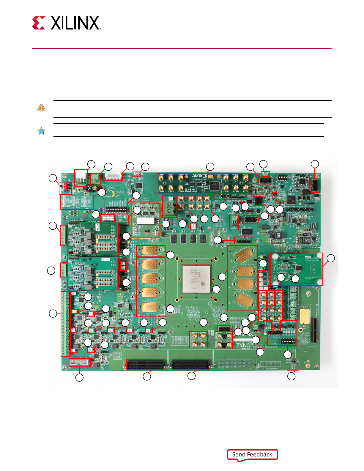
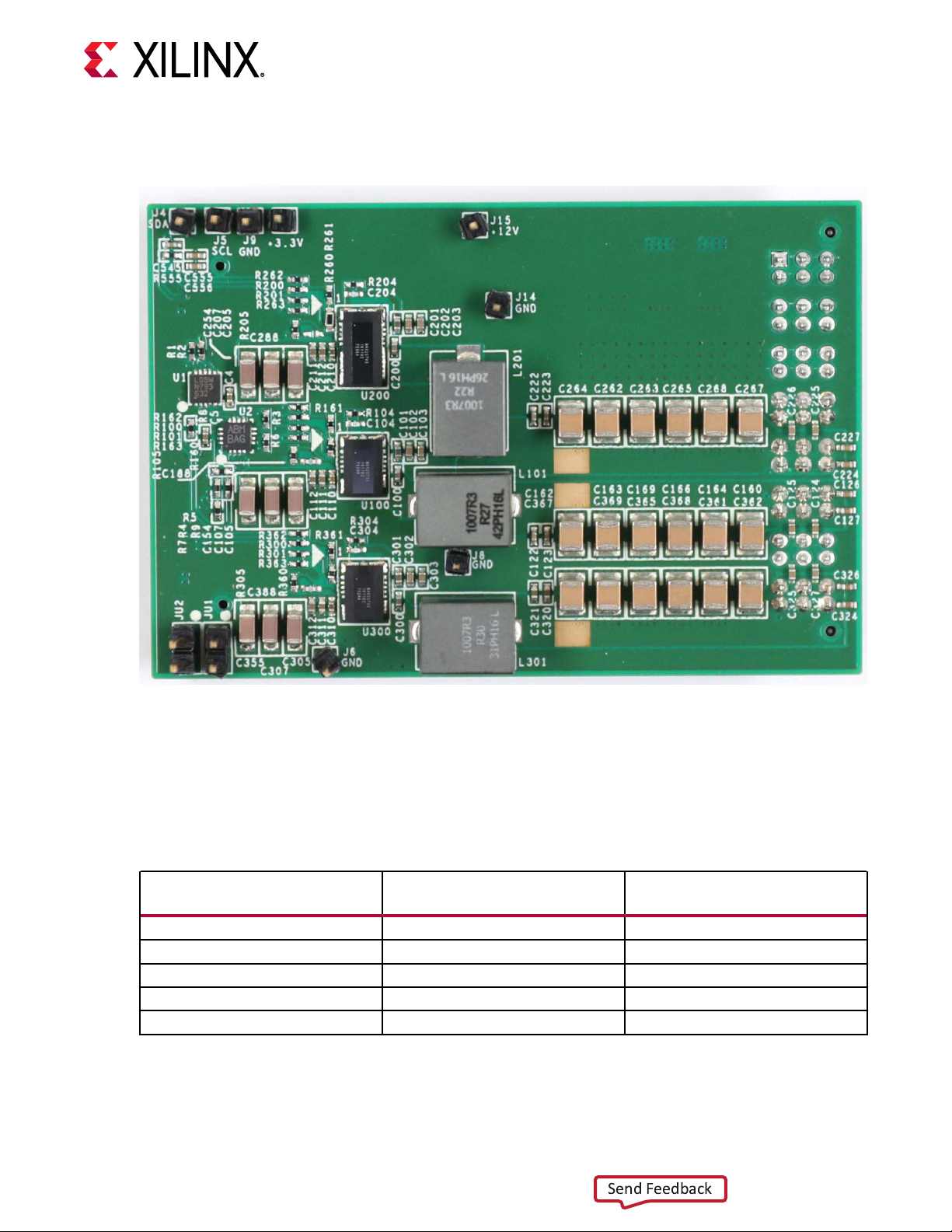
Board Component Locations
The following gure shows the ZCU1285 board component locaons. Each numbered
component shown in the gure is keyed to the table in Board Component Descripons.
CAUTION! Do not remove the rubber feet from the board. The feet provide clearance to prevent short circuits on
the back side of the board.
IMPORTANT! The following gure is for reference only and might not reect the current revision of the board.
Figure 2: Board Component Locations
2
3 5 6 7
1
23
24
26
29
31
31
30
31
31
31
31
31
4
22
21
25
27
28
31 31
15
18 17
19
20
33
34
31
16
37
36
35
51
50
13
14
47
46
49
8
10
11
12
38
39
40
48
45
44
43
9
41
UG1348 (v1.0) July 16, 2019 www.xilinx.com
ZCU1285 Board User Guide 8
32
54
53
52
X22891-060619
Page 9

Chapter 1: ZCU1285 Board Features and Operation
Send Feedback
Board Component Descriptions
Table 1: Board Component Descriptions
Callout Reference Designator Feature Description
1 SW1 Power Switch
2 J28 12V Mini-Fit connector (12V Input Power)
3 J27 12V external power supply connector (12V Input Power, Using
4 J73 ATX power connector (12V Input Power)
5 J1 USB to Quad-UART Bridge (Micro-B receptacle)
6 J36 SuperClock-2 Module (HW-CLK-101-SCLK2)
7 J3 System Controller JTAG connector
8 J69 USB-to-JTAG connector (Micro-B receptacle) (RFSoC Configuration)
9 J2 Platform USB JTAG connector (alternate access for programming
10 SW4, DS12, DS16, DS27, DS1 System Controller status LEDs and POR pushbutton (System
11 J4, J145, J154, J8 Serial transceiver power module PMBus connectors and
12 J163, J164, J166, J165 Boot Mode Selection Headers
13 J121, J125 I2C bus master selection headers (I2C Bus Management)
14 J160, J275 VTT_HP external connector and selection header
15 SW15, SW14 PS_POR_B Pushbutton and PS_SRST_B Pushbutton
16 J250, J251 VCCINT power probe SMA
17 J276, J277 VCCINT_AMS power probe SMA
18 J158, J159, J156, J194 PS-GTR ref clock SMAs (Serial Transceivers and Reference Clocks)
19 J99 Active Heat Sink and Power Connector
20 J181 VCCINT external power connector and voltage sense header
21 DS18, DS2 12V and Power Good LEDs (Power Switch)
22 SW2 Power regulation inhibitor switch for onboard regulators (Using
23 DS4–DS11, DS13–DS15, DS28– DS38,
DS42–DS45, DS49
24 J149, J148, J147 GTY voltage sense headers
25 J174, J155 GTY power module (Serial Transceiver Power Modules)
26 J150 GTY external power supply connector
27 J63, J62 PS-GTR voltage sense headers
28 J138, J93 PS-GTR power module (Serial Transceiver Power Modules)
29 J67 PS-GTR external power supply connector
30 J151, J96 RFSoC logic and processor external power supply connectors
31 J146, J144, J143, J142, J64, J23, J19, J18,
J177
32 J21 PMBus connector (Monitoring Voltage and Current)
External Power Sources)
cables) (RFSoC Configuration)
Controller Reset, System Controller Status LEDs)
isolation selection headers (Monitoring Voltage and Current)
External Power Sources)
Status LEDS for RFSoC logic, processor, transceiver, data converter,
and utility power
RFSoC logic and processor voltage sense headers
UG1348 (v1.0) July 16, 2019 www.xilinx.com
ZCU1285 Board User Guide 9
Page 10

Chapter 1: ZCU1285 Board Features and Operation
Send Feedback
Table 1: Board Component Descriptions (cont'd)
Callout Reference Designator Feature Description
33 J39 PS-GTR transceiver connector pad, bank 505 (Serial Transceivers and
34 J117, J118, J280, J281 GTY transceiver connector pads Q128, Q129, Q130, and Q131
35 U1 XCZU39DR-2FFVF1760I, Zynq UltraScale+ RFSoC
36 J124, J278, J129, J279 RF-ADC and RF-DAC Bulls Eye connector pads, tiles 224–231 (RF Data
37 J20 RF-ADC VCM connector
38 J75, J76, J78, J81, J79 RF-ADC and RF-DAC voltage sense headers
39 J46, J43, J60, J25 RF-ADC and RF-DAC PMBus connector and selection headers
40 J114, J115, J116, J107, J113 RF-ADC and RF-DAC external power supply connectors
41 J131, J119, J120 Analog Power Module
42 J170 SuperClock-RF2 Module(HW-CLK-103)
43 SW16, SW17, J95, SW3, DS22– DS26,
DS46–DS48
44 SW7 RFSoC PROGRAM Pushbutton
45 DS40, DS39, DS17, DS3 RFSoC DONE LED, INIT LED, STATUS LED, and ERROR LED
46 J106, J216 VTT_HP external connector and selection header
47 J190, J189, J188, J187, J192, J191, J257,
J256, J162, J161
48 J243, J242 RF-DAC SYSREF SMA
49 J84, J85, J83, J86 SMA connectors to differential GC pins on RFSoC (Differential SMA
50 J5 PL JTAG connector tied to RFSoC I/O pins
51 J254, J255, J253, J252 Power probe SMAs for VCCO_HP and VCCO_HD
52 J287 RFSoC SD Cardslot (bottom side of board)
53 JA3 FMC2 HPC connector tied to VCCO_HP banks (FPGA Mezzanine Card
54 JA4 FMC3 LPC connector tied to VCCO_HD banks (FPGA Mezzanine Card
Reference Clocks)
Converters and Sampling Clocks)
(Monitoring Voltage and Current)
User configurable I/O header, DIP switch, LEDs, and
pushbuttons (User LEDs, User DIP Switches and I/O Header)
Power probe SMAs for DAC_AVCC, DAC_AVTT, DAC_AVCCAUX,
ADC_AVCC, and ADC_AVCCAUX
Pin Inputs)
Interface, FMC Tab)
Interface, FMC Tab)
Power Management
UG1348 (v1.0) July 16, 2019 www.xilinx.com
ZCU1285 Board User Guide 10
12V Input Power
The ZCU1285 board receives 12V main power through J28 (callout 2, Figure 2: Board
Component Locaons) using the 12V AC adapter included with the ZCU1285 characterizaon
kit. J28 is a 6-pin (2 x 3), right angle, Mini-Fit connector.
Page 11

Chapter 1: ZCU1285 Board Features and Operation
Send Feedback
CAUTION! When supplying 12V through J28, use only the power supply provided for use with this board (Xilinx
part number 3800033).
CAUTION! Do NOT use a 6-pin, PC ATX power supply connector with J28. The pinout of the 6-pin, PC ATX
connector is not compable with J28 and the board will be damaged if an aempt is made to power it from a PC
ATX power supply connector.
12V power can also be provided through:
• Connector J73 (callout 4, Figure 2: Board Component Locaons) which accepts an ATX hard
drive 4-pin power plug
• Connector J27 (callout 3, Figure 2: Board Component Locaons) which can be connected to a
bench-top power supply
CAUTION! Because connector J73 provides no reverse polarity protecon, use a power supply with a current
limit set at 6A maximum.
CAUTION! Do NOT apply 12V power to more than a single input source. For example, do not apply power to
J73 and J27 at the same me.
CAUTION! If J73 or J27 is used to supply the 12V input power, be careful that board power consumpon does
not exceed 75W (this includes the RFSoC).
Power Switch
The ZCU1285 board main power is turned on or o using switch SW1 (callout 1, Figure 2: Board
Component Locaons). When the switch is in the ON posion, power is applied to the board and
the power good LED DS18 illuminates green (callout 21, Figure 2: Board Component Locaons).
Onboard Power Regulation
ZCU1285 Power Supply Block Diagram
The following gure shows the onboard power supply architecture.
UG1348 (v1.0) July 16, 2019 www.xilinx.com
ZCU1285 Board User Guide 11
Page 12
Chapter 1: ZCU1285 Board Features and Operation
Send Feedback
Figure 3: Board Power Supply Block Diagram
12V PWR
IN
Maxim 20751 U23
MultiPhase Master
Maxim VT1697SBFXQ U118
0.85V at 20A max
Maxim VT1697SBFXQ U137
0.85V at 20A max
Maxim VT1697SBFXQ U138
0.85V at 20A max
Maxim 15303 U24
1.8V at 6A max
Maxim 15303 U47
0.85V at 6A max
Maxim 15303 U29
1.8V at 6A max
Maxim 15303 U31
1.8V at 6A max
Maxim 15301 U28
0.85V at 12A max
Maxim 15303 U48
1.8V at 3A max
Maxim 15303 U27
1.2V at 3A max
Maxim 15303 U11
1.5V at 6A max
Maxim 15303 U96
1.8V at 6A max
Maxim 20751 U89
MultiPhase Master
Maxim VT1697SBFXQ U20
0.85V at 20A max
Maxim VT1697SBFXQ U17
0.85V at 20A max
Maxim 15301 U50
1.8V at 20A max
Maxim 15301 U51
2.5V at 12A max
Maxim 15301 U30
3.3V at 20A max
Maxim 15303 U102
5.0V at 6A max
GTY Power Module
Quads 128-131
0.9V at 12.0A max
1.2V at 20A max
1.8V at 2.5A max
VCCINT
VCCAUX / VCCAUX_IO
VCCBRAM / VCCINT_IO
VCCO_HP
VCCO_HD
VCCPINT
VCCPAUX
VCC_PSPL
VCCO_DDR
VCCO_MIO
VCCINT_AMS
UTIL_1V8
UTIL_2V5
UTIL_3V3
UTIL_5V0
MGTAVCC
MGTAVTT
MGTVCCAUX
L
UG1348 (v1.0) July 16, 2019 www.xilinx.com
ZCU1285 Board User Guide 12
TI LMZ31503 U155
5.4V at 3A max
GTR Power Module
Quad 505
0.85V at 12.0A max
1.8V at 2.5A max
Analog Power Module
Tiles 224-231
0.925V at 2.0A max
1.8V at 2A max
0.925V at 3.5A max
1.8V at 2.0A max
2.5V or 3.0V at 2.0A max
Linear Tech LT1764 U154
5.0V at 3A max
MGTAVCC_GTR
MGTAVTT_GTR
ADC_AVCC
ADC_AVCCAUX
DAC_AVCC
DAC_AVTT
DAC_AVCCAUX
UTIL_5V0_ACM
X22892-071519
Page 13

Chapter 1: ZCU1285 Board Features and Operation
Send Feedback
Onboard Power System Devices
The ZCU1285 board uses power regulators and PMBus-compliant pulse width modulaon
(PWM) digital controllers from Maxim Integrated to supply the RFSoC logic and ulity voltages
listed in the following table. The board can also be congured to use an external bench power
supply for each voltage. See Using External Power Sources.
The output voltages of the controllers in the table can be reprogrammed using the Maxim InTune
Digital PowerTool.
Note: The MAX20751EKX device has limited nonvolale memory reprogramming saves (four counts).
CAUTION! Be extremely careful when aempng to modify any of the onboard regulators, because an
incorrectly programmed regulator can damage onboard components.
Table 2: Onboard Power System Devices
Device Part Number
RFSoC Logic
Maxim MAX20751EKX
Maxim MAX15303 U24 InTune digital point of load
Maxim MAX15303 U47 InTune digital point of load
Maxim MAX15303 U29 InTune digital point of load
Maxim MAX15303 U31 InTune digital point of load
Processor
Maxim MAX15301 U28 InTune digital point of load
Maxim MAX15303 U48 InTune digital point of load
Maxim MAX15303 U27 InTune digital point of load
Maxim MAX15303 U11 InTune digital point of load
Maxim MAX15303 U96 InTune digital point of load
RF Data Converters
Maxim MAX20751EKX
INA226 U60 Current shunt and power
1
1
Reference
Designator(s)
U23 Multiphase master with
PMBus interface controller
(60A three phases at 20A/
phase)
(PoL) controller, 6A
(PoL) controller, 6A
(PoL) controller, 6A
(PoL) controller, 6A
(PoL) controller, 12A
(PoL) controller, 3A
(PoL) controller, 3A
(PoL) controller, 6A
(PoL) controller, 6A
U89 Multiphase master with
PMBus interface controller
(40A two
phases at 20A/phase)
monitor with I2C interface
Description
Power Rail Net
Name
VCCINT 0.85V
VCCAUX / VCCAUX_IO 1.8V
VCCBRAM / VCCINT_IO 0.85V
VCCO_HP 1.8V
VCCO_HD 1.8V
VCCPINT 0.85V
VCCPAUX 1.8V
VCC_PSPLL 1.2V
VCCO_DDR 1.5V
VCCO_MIO 1.8V
VCCINT_AMS 0.85V
ADC_AVCC 0.925V
Voltage
UG1348 (v1.0) July 16, 2019 www.xilinx.com
ZCU1285 Board User Guide 13
Page 14
Chapter 1: ZCU1285 Board Features and Operation
Send Feedback
Table 2: Onboard Power System Devices (cont'd)
Device Part Number
INA226 U61 Current shunt and power
INA226 U63 Current shunt and power
INA226 U64 Current shunt and power
INA226 U65 Current shunt and power
GTY Transceivers
INA226 U141 Current shunt and power
INA226 U142 Current shunt and power
INA226 U143 Current shunt and power
PS-GTR Transceivers
INA226 U99 Current shunt and power
INA226 U97 Current shunt and power
Utility
Maxim MAX15301 U50 InTune digital point of load
Maxim MAX15301 U51 InTune digital point of load
Maxim MAX15301 U30 InTune digital point of load
Maxim MAX15301 U102 InTune digital point of load
LMZ31503 U155 DC/DC converter, 3A UTIL_5V4 5.4V
LT1764 U154 Fixed LDO regulator UTIL_5V0_ACM 5.0V
System Controller
Maxim MAX15053 U13 Fixed LDO regulator SYS_1V0 1.0V
Maxim MAX15027 U25 Fixed LDO regulator VCC_1V2 1.2V
Maxim MAX15027 U33 Fixed LDO regulator VCC_1V8 1.8V
Notes:
1. The MAX20751EKX device has limited nonvolatile memory reprogramming saves (four counts).
Reference
Designator(s)
Description
monitor with I2C interface
monitor with I2C interface
monitor with I2C interface
monitor with I2C interface
monitor with I2C interface
monitor with I2C interface
monitor with I2C interface
monitor with I2C interface
monitor with I2C interface
(PoL) controller, 20A
(PoL) controller, 12A
(PoL) controller, 20A
(PoL) controller, 12A
Power Rail Net
Name
ADC_AVCCAUX 1.8V
DAC_AVCC 0.925V
DAC_AVTT 1.8V
DAC_AVCCAUX 2.5V or
MGTAVCC 0.9V
MGTAVTT 1.2V
MGTVCCAUX 1.8V
MGTAVCC_GTR 0.85V
MGTAVTT_GTR 1.8V
UTIL_1V8 1.8V
UTIL_2V5 2.5V
UTIL_3V3 3.3V
UTIL_5V0 5.0V
Voltage
3.0V
UG1348 (v1.0) July 16, 2019 www.xilinx.com
ZCU1285 Board User Guide 14
Page 15

Chapter 1: ZCU1285 Board Features and Operation
Send Feedback
Using External Power Sources
Each voltage rail for the RFSoC logic, mul-gigabit transceivers (MGTs), and RF data converters
has an associated Euro-Mag spring-clamp terminal block (callout 3, 14, 20, 26, 29, 30, 40, and 46,
Figure 2: Board Component Locaons), which can be used to provide power from an external
source (see the following table).
CAUTION! Do NOT apply power to any of the RFSoC logic external power supply connectors without rst
disabling the associated regulator or regulators. Failing to disable the regulator can damage the board.
Each onboard RFSoC logic regulator can be disabled using its respecve power regulaon inhibit DIP switch
(callout 22, Figure 2: Board Component Locaons). A regulator is enabled when the power regulaon inhibitor
switch is set to the ENABLED posion. The following table lists the external power connectors for the dierent
power rails.
Table 3: RFSoC Logic and Serial Transceiver Rails
External
Power Rail Net Name
Supply
Connector(s)
VCCINT
VCCBRAM
VCCAUX J23
VCCO_HP J19
VCCO_HD J18
RFSoC Logic and Processor
GTY Transceivers
PS-GTR Transceivers
RF Data Converters
Notes:
1. The serial transceiver or analog power module must be removed before providing external power to any of the
transceiver or data converter rails (see Serial Transceiver Power Modules).
VCCPINT J177
VCCPAUX
VCC_PSPLL J144
VCCO_DDR J143
VCCO_MIO J142
VCCINT_AMS J64
MGTAVCC
MGTAVTT J148
MGTVCCAUX J149
MGTAVCC_GTR
MGTAVTT_GTR J63
ADC_AVCC J114 J79
ADC_AVCCAUX J115 J81
DAC_AVCC J116 J75
DAC_AVTT J107 J76
DAC_AVCCAUX J113 J78
J181 J22
J96
J151
J150
J67
Remote Sense
Header
J74
J146
J147
J62
UG1348 (v1.0) July 16, 2019 www.xilinx.com
ZCU1285 Board User Guide 15
Page 16
Chapter 1: ZCU1285 Board Features and Operation
Send Feedback
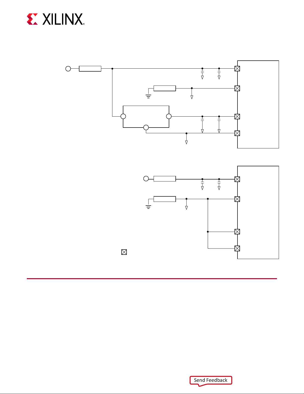
Monitoring Voltage and Current
Voltage and current monitoring and control for the Maxim power system is available through
either the ZCU1285 System Controller or via the Maxim PowerTool soware GUI.
The ZCU1285 System Controller is the simplest and most convenient way to monitor the voltage
and current values for the power rails listed in Onboard Power System Devices. For details on
how to use this built-in feature, see Power Tab.
The ZCU1285 board includes these PMBus connectors:
• J21 (callout 32, Figure 2: Board Component Locaons), for use with the Maxim USB-to-
PMBus interface dongle (Maxim part number MAXPOWERTOOL002) and the Maxim
PowerTool GUI.
• J4 and J145 (callout 11, Figure 2: Board Component Locaons) are used to connect to the
serial transceiver power module’s PMBus. The pinouts for J4 and J145 are shown in the
following gure
• J25 (callout 39, Figure 2: Board Component Locaons) is used to connect to the analog power
module PMBus. The pinout for J25 is shown in the following gure.
Figure 4: PMBus Connector Pinouts
CLK CTRL
DATA
NC
ALERT
NC
NC
NC
NC
1 2
3 4
5 6
7 8
9 10
11 12
13 14
15 16
GND
1
2
3
4
5
J4, J145
CLK
DATA
ALERT
CTRL
GND
1
2
3
4
J25
CLK
DATA
ALERT
GND
UG1348 (v1.0) July 16, 2019 www.xilinx.com
ZCU1285 Board User Guide 16
MAXPOWERTOOL002
X22893-051519
The onboard Maxim power controllers by default are isolated from the serial transceiver power
module’s PMBus. However, the two interfaces can be linked by removing the shunt on J8 or J154
(serial transceiver PMBus isolaon). This conguraon is required when using Maxim PowerTool
to monitor and control both the RFSoC power rails and the serial transceiver power rails using
the Maxim InTune Digital PowerTool GUI.
Page 17
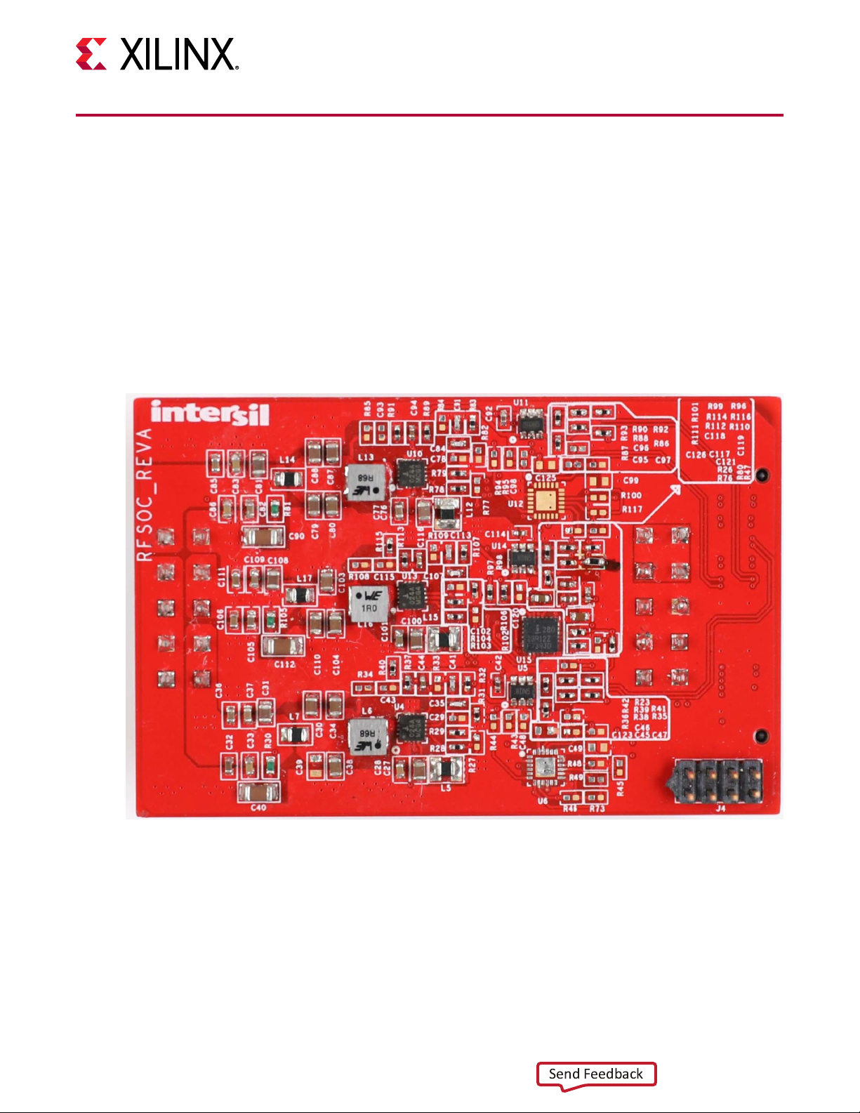
Analog Power Module
Send Feedback
There is one analog power module interface for connecng an analog power module (callout 41,
Figure 2: Board Component Locaons). The analog power module supplies power to the
ADC_AVCC, ADC_AVCCAUX, DAC_AVCC, DAC_AVTT, and DAC_AVCCAUX rails, which power
the RFSoC RF data converters. The analog power module connects to J131, J119, and J120. Two
analog power modules are provided with the ZCU1285 board for evaluaon. One module is
made by Intersil with part number ISL8024DEMO2Z and the other is made by MPS with part
number EVREF0102A. See the following two gures.
Figure 5: Intersil Analog Power Module
Chapter 1: ZCU1285 Board Features and Operation
UG1348 (v1.0) July 16, 2019 www.xilinx.com
ZCU1285 Board User Guide 17
Page 18

Chapter 1: ZCU1285 Board Features and Operation
Send Feedback
Figure 6: MPS Analog Power Module
The following table lists the nominal voltage values for the ADC_AVCC, ADC_AVCCAUX,
DAC_AVCC, DAC_AVTT, and DAC_AVCCAUX power rails. It also lists the maximum current
rang for each rail supplied by the analog power modules included with the ZCU1285
characterizaon kit.
Table 4: Analog Power Module
Analog Rail Net Name Nominal Voltage (V) Maximum Current Rating (A)
ADC_AVCC 0.925 2.00
ADC_AVCCAUX 1.8 2.00
DAC_AVCC 0.925 3.5
DAC_AVCCAUX 1.8 2.00
DAC_AVTT 2.5 or 3.0 2.00
The analog power rails can also be supplied externally. The external supply connectors are listed
in the table in Using External Power Sources.
UG1348 (v1.0) July 16, 2019 www.xilinx.com
ZCU1285 Board User Guide 18
Page 19
Chapter 1: ZCU1285 Board Features and Operation
Send Feedback
CAUTION! The analog power module MUST be removed when providing external power to the RF data
converter rails.
Informaon about the analog power modules included with the ZCU1285 characterizaon kit is
available from the vendor websites Renesas Power Management and Monolithic Power Systems
Serial Transceiver Power Modules
There is one GTY transceiver power module interface (callout 25, Figure 2: Board Component
Locaons). The GTY transceiver power module supplies the MGTAVCC, MGTAVTT, and
MGTVCCAUX power rails, which connect to the RFSoC GTY transceivers. In the ZCU1285
characterizaon kit, there is one GTY transceiver power module from Maxim Integrated provided
for evaluaon, part number MAXREFDES87#. The GTY transceiver power module is labeled GTY
and connects to J174 and J155.
There is one PS-GTR transceiver power module interface (callout 28, Figure 2: Board Component
Locaons). The PS-GTR transceiver power module supplies the MGTAVCC_GTR and
MGTAVTT_GTR power rails, which connect the RFSoC PS-GTR transceivers. In the ZCU1285
characterizaon kit, there is one PS-GTR transceiver power module from Maxim Integrated
provided for evaluaon, part number MAXREFDES87#. The PS-GTR power module is labeled
PS-GTR and connects to J138 and J93.
UG1348 (v1.0) July 16, 2019 www.xilinx.com
ZCU1285 Board User Guide 19
Page 20
Chapter 1: ZCU1285 Board Features and Operation
Send Feedback
Figure 7: Maxim Integrated Serial Transceiver Power Module
UG1348 (v1.0) July 16, 2019 www.xilinx.com
ZCU1285 Board User Guide 20
The following table lists the nominal voltage values for the MGTAVCC, MGTAVTT,
MGTVCCAUX, MGTAVCC_GTR, and MGTAVTT_GTR power rails. It also lists the maximum
current rang for each rail supplied by serial transceiver modules included with the ZCU1285
board.
Table 5: Serial Transceiver Power Modules
Serial Transceiver Rail Net
Name
MGTAVCC 0.9 12
MGTAVTT 1.2 20
MGTVCCAUX 1.8 2.5
MGTAVCC_GTR 0.85 12
MGTAVTT_GTR 1.8 2.5
Nominal Voltage (V) Maximum Current Rating (A)
The serial transceiver power rails can also be supplied externally. The external supply connectors
are listed in the table in Using External Power Sources.
Page 21

CAUTION! The serial transceiver power module MUST be removed when providing external power to the GTY or
Send Feedback
PS-GTR transceiver rails.
Note: For informaon about the serial transceiver power modules, contact Maxim technical support and
ask about the MAXREFDES87#.
Zynq UltraScale+ RFSoC
The ZCU1285 board is populated with the XCZU39DR-2FFVF1760I Zynq UltraScale+ RFSoC at
U1 (callout 35, Figure 2: Board Component Locaons). For further informaon on Zynq
UltraScale+ RFSoCs, see the UltraScale Architecture and Product Data Sheet: Overview (DS890).
RFSoC Configuration
The RFSoC is congured using one of the following opons:
Chapter 1: ZCU1285 Board Features and Operation
• Digilent embedded USB JTAG connector (callout 8, Figure 2: Board Component Locaons)
• Xilinx Plaorm Cable USB II JTAG cable connector (callout 9, Figure 2: Board Component
Locaons)
The ZCU1285 board comes with an embedded USB-to-JTAG conguraon module (Digilent, J69)
which allows a host computer to access the board JTAG chain using a Standard A to Micro-B
USB cable. Alternately, a JTAG connector (J2) is available to provide access to the JTAG chain
using the Xilinx Plaorm Cable USB II or compable conguraon cable.
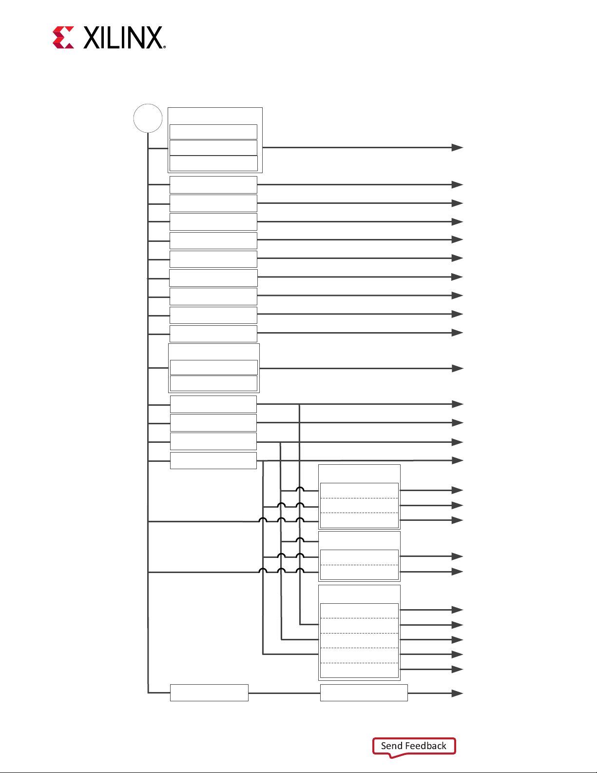
The JTAG chain of the board is illustrated in the following gure. By default, only the RFSoC is in
the chain. Installing a shunt at J6 adds the FMC interfaces to the chain.
UG1348 (v1.0) July 16, 2019 www.xilinx.com
ZCU1285 Board User Guide 21
Page 22
Chapter 1: ZCU1285 Board Features and Operation
Send Feedback
Figure 8: JTAG Chain
Xilinx
System Controller
XC7Z010-CLG225
Bank 34 (1.8V)
USB-JTAG
Module
MICRO-B
USB Conn.
1.8V
SYS_TCK
SYS_TMS
SYS_TDI
SYS_TDO
JTAG
Conn.
1.8V
VCCO_MIO
3.3V
DUT_TDI
FMC_TCK
FMC_TMS
Connector
(not populated)
FMC1_TDI
FMC1
VCCO_MIO
2:1
MUX
FMC2_TDI FMC3_TDI
TDI_0
FMC3_TDO
FMC2
Connector
(VCCO_HP)
TMS_0
TDO_0
FMC3
Connector
(VCCO_HD)
Bank 503 (VCCO_MIO)
PROGRAM Pushbutton
Pressing the PROGRAM pushbuon SW7 (callout 44, Figure 2: Board Component Locaons)
asserts the acve-Low program pin of the RFSoC.
Xilinx
Zynq
UltraScale+
RFSoC
X22890-060719
DONE LED
The DONE LED DS17 (callout 45, Figure 2: Board Component Locaons) indicates the state of
the DONE pin of the RFSoC. When the DONE pin is High, DS17 lights up, indicang the RFSoC
is successfully congured.
INIT LED
The dual-color INIT LED DS3 (callout 45, Figure 2: Board Component Locaons) indicates the
RFSoC inializaon status. During RFSoC inializaon the INIT LED illuminates red. When
RFSoC inializaon has completed, the LED illuminates green.
STATUS LED
The STATUS LED DS39 (callout 45, Figure 2: Board Component Locaons) indicates a secure
lockdown state. When the PS_ERROR_STATUS pin is High, DS39 lights up.
UG1348 (v1.0) July 16, 2019 www.xilinx.com
ZCU1285 Board User Guide 22
Page 23
Chapter 1: ZCU1285 Board Features and Operation
Send Feedback
ERROR LED
The ERROR LED DS40 (callout 45, Figure 2: Board Component Locaons) indicates an accidental
loss of power, an error, or an excepon in the RFSoC processor PMU. When the
PS_ERROR_OUT pin is High, DS40 lights up.
PS_POR_B Pushbutton
Pressing the PS_POR_B pushbuon SW14 (callout 15, Figure 2: Board Component Locaons)
asserts the acve-Low PS_POR_B pin of the RFSoC processor.
PS_SRST_B Pushbutton
Pressing the PS_SRST_B pushbuon SW15 (callout 15, Figure 2: Board Component Locaons)
asserts the acve-Low PS_SRST_B pin of the RFSoC processor.
Boot Mode Selection Headers
Four 3-pin headers are provided for mode pin selecon to set the boot mode for the RFSoC
processor (callout 12, Figure 2: Board Component Locaons). Install a jumper across pins 1–2
(MIO_BUS) to set a 1, and pins 2–3 (GND) to set a 0. See the following table for a complete list
of boot mode sengs.
Table 6: Boot Mode Selection
Boot Mode MODE 3 (J163) MODE 2 (J164) MODE 1 (J166) MODE 0 (J165)
JTAG 0 0 0 0
QSPI24 0 0 0 1
QSPI32 0 0 1 0
1
SD0
1
NAND
1
SD1
eMMC_18
USB 0
PJTAG_0
PJTAG_1
SD1-LS 1 1 1 0
Notes:
1. These boot modes are not directly supported by the ZCU1285 board.
1
1
1
1
0 0 1 1
0 1 0 0
0 1 0 1
0 1 1 0
0 1 1 1
1 0 0 0
1 0 0 1
UG1348 (v1.0) July 16, 2019 www.xilinx.com
ZCU1285 Board User Guide 23
Page 24

Chapter 1: ZCU1285 Board Features and Operation
Send Feedback
RFSoC Processor Reference Clock
A free-running 33.3333333 MHz clock (U12) is the clock source for the RFSoC processor
(PS_REF_CLK).
300 MHz LVDS Oscillator
A 300 MHz LVDS oscillator U145 (SiTime SIT9107AI-243N25E300.0000) connects to global
clock (GC) pins on the RFSoC. The following table lists the RFSoC pin connecons to the LVDS
oscillator.
Table 7: LVDS Oscillator GC Connections
RFSoC (U1)
Pin Function Direction
AP22 SYSTEM
CLOCK_P
AR22 SYSTEM
CLOCK_N
Input LVDS LVDS_OSC_P 4 300 MHz LVDS
Input LVDS LVDS_OSC_N 5 300 MHz LVDS
I/O
Standard
Schematic
Net Name
Pin Function Direction
Device (U145)
Output
oscillator
Output
oscillator
Differential SMA Pin Inputs
Two pairs of SMA connectors (callout 49, Figure 2: Board Component Locaons) provide access
to global clock (GC) pins on the RFSoC. The GC pins are connected to the SMA connectors as
shown in the following table.
Table 8: Differential SMA Clock Connections
RFSoC (U1)
Pin Function Direction IOSTANDARD
AP26 USER CLOCK_1_P Input LVDS CLK_DIFF_1_P J84
AR26 USER CLOCK_1_N Input LVDS CLK_DIFF_1_N J85
AT23 USER CLOCK_2_P Input LVDS CLK_DIFF_2_P J83
AT24 USER CLOCK_2_N Input LVDS CLK_DIFF_2_N J86
Schematic Net
Name
SMA Connector
UG1348 (v1.0) July 16, 2019 www.xilinx.com
ZCU1285 Board User Guide 24
User LEDs
Eight acve-High LEDs, DS22 through DS26, and DS46 through DS48 (callout 43, Figure
2: Board Component Locaons), are connected to GPIO pins on the RFSoC. These LEDs can be
used to indicate status or other funcons. Their pinout is listed in the following table.
Page 25
Table 9: User LEDs
Send Feedback
Chapter 1: ZCU1285 Board Features and Operation
RFSoC (U1)
Pin Function Direction IOSTANDARD
AM25 USER LED Output LVCMOS18 APP_LED1 DS26
AL24 USER LED Output LVCMOS18 APP_LED2 DS22
AK22 USER LED Output LVCMOS18 APP_LED3 DS23
AJ22 USER LED Output LVCMOS18 APP_LED4 DS24
AN25 USER LED Output LVCMOS18 APP_LED5 DS25
AN24 USER LED Output LVCMOS18 APP_LED6 DS46
AM23 USER LED Output LVCMOS18 APP_LED7 DS47
AL23 USER LED Output LVCMOS18 APP_LED8 DS48
Schematic Net
Name
Reference
Designator
User DIP Switches and I/O Header
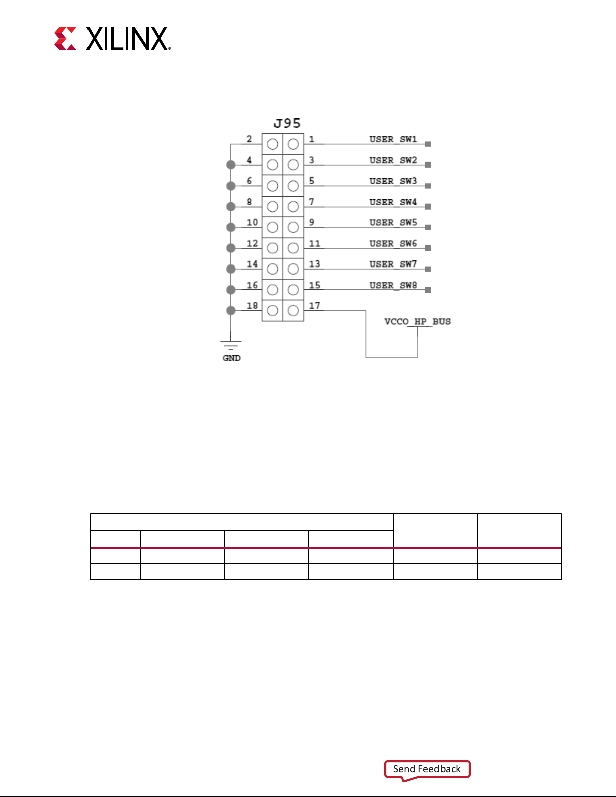
The DIP switch SW3 (callout 43, Figure 2: Board Component Locaons) provides a set of eight
acve-High switches that connect to user I/O pins on the RFSoC as shown in the following table.
Use these pins to set control pins or for any other purpose. The eight I/Os also map to test
header J95 (callout 43, Figure 2: Board Component Locaons), providing external access for
these pins. The I/O pins can be connected to the onboard System Controller as addional GPIO
between the two devices.
Note: Install J7 to connect the user DIP switches to the System Controller.
Table 10: User DIP Switches
RFSoC (U1)
Pin Function Direction IOStandard
AV25 User Switch Input LVCMOS18 USER_SW1
AU25 User Switch Input LVCMOS18 USER_SW2 3 E13
AV23 User Switch Input LVCMOS18 USER_SW3 5 E11
AU23 User Switch Input LVCMOS18 USER_SW4 7 E12
AW24 User Switch Input LVCMOS18 USER_SW5 9 F13
AV24 User Switch Input LVCMOS18 USER_SW6 11 F14
BA22 User Switch Input LVCMOS18 USER_SW7 13 G15
AY22 User Switch Input LVCMOS18 USER_SW8 15 F15
Schematic
Net Name
DIP Switch
Reference
Designator
SW3
J95 Test
Header Pin
1
Device
(U38) Pin
F12
The following gure shows the user I/O connector J95 (callout 43, Figure 2: Board Component
Locaons).
UG1348 (v1.0) July 16, 2019 www.xilinx.com
ZCU1285 Board User Guide 25
Page 26
Chapter 1: ZCU1285 Board Features and Operation
Send Feedback
Figure 9: User I/O Connector J95
User Pushbuttons
SW16 and SW17 (callout 43, Figure 2: Board Component Locaons) are acve-High user
pushbuons that are connected to RFSoC I/O pins as shown in the following table. These
pushbuons can be used for any user-determined purpose.
Table 11: User Pushbuttons
RFSoC (U1)
Pin Function Direction IOSTANDARD
AM22 User pushbutton Input LVCMOS18 USER_PB1 SW16
AN26 User pushbutton Input LVCMOS18 USER_PB2 SW17
Schematic Net
Name
Reference
Designator
System Monitor
The System Monitor (SYSMON) monitors the physical environment using on-chip temperature
and supply sensors, up to 17 external analog inputs, and an integrated analog-to-digital converter
(ADC). There is a separate SYSMON for the PL and the PS. The PS SYSMON is powered using
the on-chip reference voltage (V
regulator. See the following gure for connecon details. More informaon about the system
monitor is available in the UltraScale Architecture System Monitor User Guide (UG580).
), and the PL SYSMON is powered using an external 1.25V
REF
UG1348 (v1.0) July 16, 2019 www.xilinx.com
ZCU1285 Board User Guide 26
Page 27
VCCAUX
Send Feedback
(1.8V +/- 3%)
Chapter 1: ZCU1285 Board Features and Operation
Figure 10: PL and PS SYSMON Power Connections
VCCAUX
Supply Filter
470 nF 100 nF
VCCADC
Digital
GND
1.25 +/- 0.2%
50 ppm /*C
VCCPAUX
(1.8V +/- 3%)
Digital
GND
Regulated
Analog
GND
VCCPAUX
Supply Filter
Analog
GND
Analog
GND
100 nF
10 µF 100 nF
100 nF
470 nF 100 nF
GNDADC
VREFP
VREFN
VCC_PSADC
(Zync UltraScale+
MPSoC only)
GND_PSADC
(Zync UltraScale+
MPSoC only)
VREFP
Quad SPI Flash Memory
UG1348 (v1.0) July 16, 2019 www.xilinx.com
ZCU1285 Board User Guide 27
Package Pins
VREFN
X22896-051519
A single quad SPI device (MT25QU01GBBB8ESF-0SIT 1.8V) is available for boong the RFSoC.
To enable QSPI, boot shunts must be installed as indicated in the table in Boot Mode Selecon
Headers.
Page 28

SD Card
Send Feedback
An SD card slot is provided (callout 52, Figure 2: Board Component Locaons) for boong the
RFSoC. The ZCU1285 board supports SD 3.0 and has an SD 3.0 compliant voltage level shier.
To enable SD boot, shunts must be installed for SD1-LS boot mode as indicated in the table in
Boot Mode Selecon Headers.
DDR3 Memory
The board provides 2 GB of DDR3 memory ulizing a 64-bit bus and running at 2133 Mb/s. The
memory system is composed of four x16 Samsung 4 Gb, 1.5V K4B4G1646D-BCNB devices. The
memory is accessible through the processing system (PS) of the Zynq UltraScale+ RFSoC.
Chapter 1: ZCU1285 Board Features and Operation
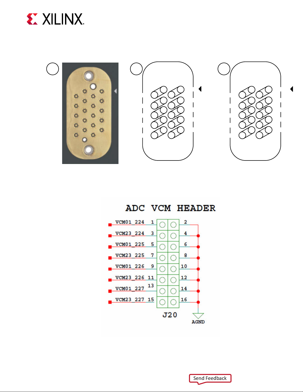
RF Data Converters and Sampling Clocks
The ZCU1285 board provides access to all of the RFSoC RF-ADC and RF-DAC signal and clock
pins. Each RF-ADC and RF-DAC is designed with –70 db isolaon at 3 GHz. The four RF-ADC
les (224, 225, 226, and 227) are brought out to two Bulls Eye connectors and a header for the
VCM pins (callout 36 and 37, Figure 2: Board Component Locaons). The four RF-DAC les (228,
229, 230, and 231) are brought out to two Bulls Eye connectors and an SMA pair for SYSREF
(callout 36 and 48, Figure 2: Board Component Locaons). The pinouts for the RF-ADC and RF-
DAC Bulls Eye connectors, and the pinout for the VCM connector are shown in the following
gures.
UG1348 (v1.0) July 16, 2019 www.xilinx.com
ZCU1285 Board User Guide 28
Page 29
Chapter 1: ZCU1285 Board Features and Operation
Send Feedback
Figure 11: A: Bulls Eye Connector Pad. B: RF-ADC Connector Pinout. C: RF-DAC
Connector Pinout
Bulls Eye Connector Pad
B
VIN_3
P
N
VIN_0
P
N
VIN_1
VIN_2
VIN_3
CLK
RF-ADC Connector Pinout RF-DAC Connector Pinout
P
N
P
N
P
N
P
N
VIN_2
P
N
N
N
N
VIN_1
P
VIN_0
P
CLK
P
Figure 12: RF-ADC VCM Header Pinout
CA
VOUT_0
VOUT_1
VOUT_2
VOUT_3
CLK
VOUT_3
P
N
P
N
P
N
P
N
P
N
P
N
VOUT_2
P
N
N
N
N
P
P
P
VOUT_1
VOUT_0
CLK
X22897-051519
UG1348 (v1.0) July 16, 2019 www.xilinx.com
ZCU1285 Board User Guide 29
Page 30

Chapter 1: ZCU1285 Board Features and Operation
Send Feedback
RF-ADC Pins
The informaon for each RF-ADC pin is listed in the following table.
Table 12: RF-ADC Pins
RFSoC (U1) Net Name Tile Connector Trace Length (mils)
AU5 ADC_VIN0_224_P 224 J124 3283.024
AU4 ADC_VIN0_224_N 224 J124 3280.721
AU2 ADC_VIN1_224_P 224 J124 3138.125
AU1 ADC_VIN1_224_N 224 J124 3135.787
AR5 ADC_VIN2_224_P 224 J124 3277.759
AR4 ADC_VIN2_224_N 224 J124 3275.53
AR2 ADC_VIN3_224_P 224 J124 3164.561
AR1 ADC_VIN3_224_N 224 J124 3162.691
BA3 ADC_CLK_224_P 224 J124 3283.463
BB3 ADC_CLK_224_N 224 J124 3279.967
AJ11 VCM01_224 224 J20 -
AJ10 VCM23_224 224 J20 -
AF9 ADC_REXT_224 224 J127 -
AN5 ADC_VIN0_225_P 225 J124 3309.41
AN4 ADC_VIN0_225_N 225 J124 3307.012
AN2 ADC_VIN1_225_P 225 J124 3196.802
AN1 ADC_VIN1_225_N 225 J124 3194.401
AL5 ADC_VIN2_225_P 225 J124 3342.156
AL4 ADC_VIN2_225_N 225 J124 3339.779
AL2 ADC_VIN3_225_P 225 J124 3223.9
AL1 ADC_VIN3_225_N 225 J124 3221.624
AW4 ADC_CLK_225_P 225 J124 3280.453
AY4 ADC_CLK_225_N 225 J124 3279.826
AH11 VCM01_225 225 J20 -
AH10 VCM23_225 225 J20 -
AJ5 ADC_VIN0_226_P 226 J278 3360.63
AJ4 ADC_VIN0_226_N 226 J278 3358.274
AJ2 ADC_VIN1_226_P 226 J278 3242.988
AJ1 ADC_VIN1_226_N 226 J278 3240.685
AG5 ADC_VIN2_226_P 226 J278 3376.291
AG4 ADC_VIN2_226_N 226 J278 3374.059
AG2 ADC_VIN3_226_P 226 J278 3253.421
AG1 ADC_VIN3_226_N 226 J278 3253.248
BA5 ADC_CLK_226_P 226 J278 3091.053
BB5 ADC_CLK_226_N 226 J278 3088.424
UG1348 (v1.0) July 16, 2019 www.xilinx.com
ZCU1285 Board User Guide 30
Page 31

Chapter 1: ZCU1285 Board Features and Operation
Send Feedback
Table 12: RF-ADC Pins (cont'd)
RFSoC (U1) Net Name Tile Connector Trace Length (mils)
AJ8 VCM01_226 226 J20 -
AJ7 VCM23_226 226 J20 -
AE5 ADC_VIN0_227_P 227 J278 3393.677
AE4 ADC_VIN0_227_N 227 J278 3391.355
AE2 ADC_VIN1_227_P 227 J278 3274.172
AE1 ADC_VIN1_227_N 227 J278 3272.253
AC5 ADC_VIN2_227_P 227 J278 3399.961
AC4 ADC_VIN2_227_N 227 J278 3397.632
AC2 ADC_VIN3_227_P 227 J278 3288.831
AC1 ADC_VIN3_227_N 227 J278 3286.82
AW6 ADC_CLK_227_P 227 J278 3095.716
AY6 ADC_CLK_227_N 227 J278 3099.089
AH8 VCM01_227 227 J20 -
AH7 VCM23_227 227 J20 -
RF-DAC Pins
The informaon for each RF-DAC pin is listed in the following table.
Table 13: RF-DAC Pins
RFSoC (U1) Net Name Tile Connector Trace Length (mils)
Y5 DAC_VOUT0_228_P 228 J129 3366.712
Y4 DAC_VOUT0_228_N 228 J129 3364.991
Y2 DAC_VOUT1_228_P 228 J129 3209.197
Y1 DAC_VOUT1_228_N 228 J129 3207.209
V5 DAC_VOUT2_228_P 228 J129 3349.961
V4 DAC_VOUT2_228_N 228 J129 3347.9
V2 DAC_VOUT3_228_P 228 J129 3192.969
V1 DAC_VOUT3_228_N 228 J129 3190.879
B3 DAC_CLK_228_P 228 J129 3340.507
A3 DAC_CLK_228_N 228 J129 3343.285
D2 SYSREF_228_P 228 J242 -
D1 SYSREF_228_N 228 J243 -
U9 DAC_REXT_228 228 J128 -
T5 DAC_VOUT0_229_P 229 J129 3319.868
T4 DAC_VOUT0_229_N 229 J129 3317.681
T2 DAC_VOUT1_229_P 229 J129 3178.213
T1 DAC_VOUT1_229_N 229 J129 3176.101
UG1348 (v1.0) July 16, 2019 www.xilinx.com
ZCU1285 Board User Guide 31
Page 32

Chapter 1: ZCU1285 Board Features and Operation
Send Feedback
Table 13: RF-DAC Pins (cont'd)
RFSoC (U1) Net Name Tile Connector Trace Length (mils)
P5 DAC_VOUT2_229_P 229 J129 3320.982
P4 DAC_VOUT2_229_N 229 J129 3319.001
P2 DAC_VOUT3_229_P 229 J129 3163.2
P1 DAC_VOUT3_229_N 229 J129 3165.4
D4 DAC_CLK_229_P 229 J129 3556.617
C4 DAC_CLK_229_N 229 J129 3560.447
M5 DAC_VOUT0_230_P 230 J279 3267.684
M4 DAC_VOUT0_230_N 230 J279 3265.525
M2 DAC_VOUT1_230_P 230 J279 3152.804
M1 DAC_VOUT1_230_N 230 J279 3150.782
K5 DAC_VOUT2_230_P 230 J279 3287.039
K4 DAC_VOUT2_230_N 230 J279 3284.711
K2 DAC_VOUT3_230_P 230 J279 3141.679
K1 DAC_VOUT3_230_N 230 J279 3139.098
B5 DAC_CLK_230_P 230 J279 3615.019
A5 DAC_CLK_230_N 230 J279 3619.695
H5 DAC_VOUT0_231_P 231 J279 3265.511
H4 DAC_VOUT0_231_N 231 J279 3263.254
H2 DAC_VOUT1_231_P 231 J279 3111.166
H1 DAC_VOUT1_231_N 231 J279 3108.992
F5 DAC_VOUT2_231_P 231 J279 3243.78
F4 DAC_VOUT2_231_N 231 J279 3241.56
F2 DAC_VOUT3_231_P 231 J279 3071.556
F1 DAC_VOUT3_231_N 231 J279 3069.35
D6 DAC_CLK_231_P 231 J279 3834.883
C6 DAC_CLK_231_N 231 J279 3835.078
Serial Transceivers and Reference Clocks
UG1348 (v1.0) July 16, 2019 www.xilinx.com
ZCU1285 Board User Guide 32
The ZCU1285 board provides access to all GTY and PS-GTR transceiver and reference clock pins
of the RFSoC (callout 33 and 34, Figure 2: Board Component Locaons). The serial transceivers
are grouped into ve sets of four TX-RX lanes, referred to as Quads. There are four GTY Quads
(Q128 –Q131), and one PS-GTR Quad (bank 505).
Page 33

Chapter 1: ZCU1285 Board Features and Operation
Send Feedback
All GTY and PS-GTR Quads and their associated reference clocks (CLK0 and CLK1) are brought
out to a connector pad, which interfaces with Samtec Bulls Eye connectors used with the Samtec
RSP-200723-02-BEYE cable assembly. Contact Samtec, Inc. for informaon about this or other
cable assemblies. In the following gure, A shows the connector pad and B shows the connector
pinout.
Figure 13: Serial Transceiver Connector Pad and Pinout
BA
CLK1
P
N
N
N
N
N
RX3
P
TX3
P
TX2
P
RX2
P
CLK0
RX0
TX0
TX1
RX1
N
P
N
P
N
P
N
P
N
P
Serial Transceiver
Connector Pinout
X22898-051519
PS-GTR bank 505 has two
Serial Transceiver
Connector Pad
addional reference clocks (CLK2 and CLK3) which are brought out to
two pairs of SMA connectors (callout 18, Figure 2: Board Component Locaons).
GTY Transceiver Pins
The informaon for each GTY transceiver pin is shown in the following table.
Table 14: GTY Transceiver Pins
RFSoC (U1) Net Name Quad Connector
AC42 128_RX0_N 128 J117 2707.458
AC41 128_RX0_P 128 J117 2707.296
AB40 128_RX1_N 128 J117 3507.681
AB39 128_RX1_P 128 J117 3508.445
AA42 128_RX2_N 128 J117 2940.702
AA41 128_RX2_P 128 J117 2938.24
Y40 128_RX3_N 128 J117 2644.503
Y39 128_RX3_P 128 J117 2647.811
Trace Length
(mils)
UG1348 (v1.0) July 16, 2019 www.xilinx.com
ZCU1285 Board User Guide 33
Page 34

Table 14: GTY Transceiver Pins (cont'd)
Send Feedback
Chapter 1: ZCU1285 Board Features and Operation
RFSoC (U1) Net Name Quad Connector
V39 128_TX0_N 128 J117 3148.266
V38 128_TX0_P 128 J117 3147.413
U37 128_TX1_N 128 J117 3228.503
U36 128_TX1_P 128 J117 3229.157
T39 128_TX2_N 128 J117 3053.346
T38 128_TX2_P 128 J117 3057.162
R37 128_TX3_N 128 J117 2914.568
R36 128_TX3_P 128 J117 2917.948
W42 129_RX0_N 129 J118 2336.327
W41 129_RX0_P 129 J118 2336.177
U42 129_RX1_N 129 J118 2915.189
U41 129_RX1_P 129 J118 2915.033
R42 129_RX2_N 129 J118 2660.231
R41 129_RX2_P 129 J118 2663.549
N42 129_RX3_N 129 J118 2191.652
N41 129_RX3_P 129 J118 2194.96
P39 129_TX0_N 129 J118 2580.324
P38 129_TX0_P 129 J118 2579.92
N37 129_TX1_N 129 J118 2828.966
N36 129_TX1_P 129 J118 2829.422
M39 129_TX2_N 129 J118 2684.658
M38 129_TX2_P 129 J118 2688.416
L37 129_TX3_N 129 J118 2565.464
L36 129_TX3_P 129 J118 2564.925
L42 130_RX0_N 130 J280 2169.162
L41 130_RX0_P 130 J280 2168.011
J42 130_RX1_N 130 J280 2753.85
J41 130_RX1_P 130 J280 2753.847
G42 130_RX2_N 130 J280 2708.119
G41 130_RX2_P 130 J280 2710.988
F40 130_RX3_N 130 J280 2298.952
F39 130_RX3_P 130 J280 2302.779
K39 130_TX0_N 130 J280 2503.962
K38 130_TX0_P 130 J280 2502.727
J37 130_TX1_N 130 J280 2738.854
J36 130_TX1_P 130 J280 2738.821
H39 130_TX2_N 130 J280 2660.143
H38 130_TX2_P 130 J280 2659.72
Trace Length
(mils)
UG1348 (v1.0) July 16, 2019 www.xilinx.com
ZCU1285 Board User Guide 34
Page 35

Table 14: GTY Transceiver Pins (cont'd)
Send Feedback
Chapter 1: ZCU1285 Board Features and Operation
RFSoC (U1) Net Name Quad Connector
G37 130_TX3_N 130 J280 2877.072
G36 130_TX3_P 130 J280 2877.059
E42 131_RX0_N 131 J281 2585.706
E41 131_RX0_P 131 J281 2585.352
D40 131_RX1_N 131 J281 3037.05
D39 131_RX1_P 131 J281 3034.196
C42 131_RX2_N 131 J281 3275.72
C41 131_RX2_P 131 J281 3274.21
B40 131_RX3_N 131 J281 2676.92
B39 131_RX3_P 131 J281 2675.781
F35 131_TX0_N 131 J281 2940.112
F34 131_TX0_P 131 J281 2939.226
E37 131_TX1_N 131 J281 3346.063
E36 131_TX1_P 131 J281 3345.916
C37 131_TX2_N 131 J281 3431.684
C36 131_TX2_P 131 J281 3432.171
A37 131_TX3_N 131 J281 3180.526
A36 131_TX3_P 131 J281 3181.286
Trace Length
(mils)
GTY Transceiver Reference Clock Inputs
Informaon for each GTY transceiver clock input is shown in the following table.
Table 15: GTY Transceiver Reference Clock Inputs
RFSoC (U1) Net Name Quad Connector
AA36 128_REFCLK0_N 128 J117
AA37 128_REFCLK0_P 128 J117
Y34 128_REFCLK1_N 128 J117
Y35 128_REFCLK1_P 128 J117
V34 129_REFCLK0_N 129 J118
V35 129_REFCLK0_P 129 J118
T34 129_REFCLK1_N 129 J118
T35 129_REFCLK1_P 129 J118
P34 130_REFCLK0_N 130 J280
P35 130_REFCLK0_P 130 J280
M34 130_REFCLK1_N 130 J280
M35 130_REFCLK1_P 130 J280
UG1348 (v1.0) July 16, 2019 www.xilinx.com
ZCU1285 Board User Guide 35
Page 36

Chapter 1: ZCU1285 Board Features and Operation
Send Feedback
Table 15: GTY Transceiver Reference Clock Inputs (cont'd)
RFSoC (U1) Net Name Quad Connector
K34 131_REFCLK0_N 131 J281
K35 131_REFCLK0_P 131 J281
H34 131_REFCLK1_N 131 J281
H35 131_REFCLK1_P 131 J281
PS-GTR Transceiver Pins
Informaon for each PS-GTR transceiver pin is shown in the following table.
Table 16: PS-GTR Transceiver Pins
RFSoC (U1) Net Name Bank Connector
AJ42 PS_RX0_N 505 J39 3920.298
AJ41 PS_RX0_P 505 J39 3918.182
AH40 PS_RX1_N 505 J39 4537.184
AH39 PS_RX1_P 505 J39 4537.361
AG42 PS_RX2_N 505 J39 4299.2
AG41 PS_RX2_P 505 J39 4302.524
AE42 PS_RX3_N 505 J39 3174.371
AE41 PS_RX3_P 505 J39 3173.868
AH36 PS_TX0_N 505 J39 3400.509
AH35 PS_TX0_P 505 J39 3399.45
AG38 PS_TX1_N 505 J39 3468.187
AG37 PS_TX1_P 505 J39 3467.251
AF40 PS_TX2_N 505 J39 3721.249
AF39 PS_TX2_P 505 J39 3724.655
AE38 PS_TX3_N 505 J39 3301.206
AE37 PS_TX3_P 505 J39 3304.523
Trace Length
(mils)
UG1348 (v1.0) July 16, 2019 www.xilinx.com
ZCU1285 Board User Guide 36
PS-GTR Transceiver Reference Clock Inputs
Informaon for each PS-GTR transceiver clock input is shown in the following table.
Table 17:
PS-GTR Transceiver Reference Clock Inputs
RFSoC (U1) Net Name Bank Connector
AF34 PS_REFCLK0_P 505 J39
AF35 PS_REFCLK0_N 505 J39
AD34 PS_REFCLK1_P 505 J39
Page 37

Table 17: PS-GTR Transceiver Reference Clock Inputs (cont'd)
Send Feedback
RFSoC (U1) Net Name Bank Connector
AD35 PS_REFCLK1_N 505 J39
AC36 PS_REFCLK2_P 505 J194
AC37 PS_REFCLK2_N 505 J156
AB34 PS_REFCLK3_P 505 J158
AB35 PS_REFCLK3_N 505 J159
SuperClock-2 Module
The SuperClock-2 Module (callout 6, Figure 2: Board Component Locaons) connects to the
clock module interface connector (J36) and provides a programmable, low-noise and low-jier
clock source for use with the GTY and PS-GTR transceivers. The clock module maps to the
RFSoC by way of two I2C signals, two LVDS pairs, and one global clock pair. The following table
lists the RFSoC mapping for the SuperClock-2 Module interface. To program the SuperClock-2
Module using the System Controller, see Appendix E: System Controller. To connect to the
SuperClock-2 Module using the I2C bus, see I2C Bus Management.
Chapter 1: ZCU1285 Board Features and Operation
Table 18: SuperClock-2 Interface Connections
RFSoC (U1)
Pin Function Direction
L28 Clock recovery Input LVDS CM_LVDS1_P 1 Clock recovery Output
L29 Clock recovery Input LVDS CM_LVDS1_N 3 Clock recovery Output
H10 Clock recovery Input LVDS CM_LVDS2_P 9 Clock recovery Output
H9 Clock recovery Input LVDS CM_LVDS2_N 11 Clock recovery Output
AP24 Global clock Input LVDS CM_GCLK_P 25 Global clock Output
AR24 Global clock Input LVDS CM_GCLK_N 27 Global clock Output
AM26 Control I/O Bidir LVCMOS CM_I2C_SCL/
AP23 Control I/O Bidir LVCMOS CM_I2C_SDA/
IOSTANDAR
D
Schematic Net
Name
DUT_PMBUS_CLK
DUT_PMBUS_DATA
Pin Function Direction
62 I2C Bidir
64 I2C Bidir
J36 Pin
UG1348 (v1.0) July 16, 2019 www.xilinx.com
ZCU1285 Board User Guide 37
Page 38

SuperClock-RF2 Module
Send Feedback
The SuperClock-RF2 Module (callout 42, Figure 2: Board Component Locaons) connects to the
clock module interface connector (J170) and provides a programmable, ultra low-noise and low-
jier wideband RF clock source intended for use with the RFSoC RF data converters. It provides
three phase-aligned LVDS reference clocks, one single-ended LVCMOS reference clock, four
dierenal pair RF clocks for RF-ADCs, and four dierenal pair RF clocks for RF-DACs. The
SuperClock-RF2 module schemac, BOM, and Allegro board les are in the XTP document
package on the Zynq UltraScale+ RFSoC ZCU1285 Characterizaon Kit website. The
SuperClock-RF2 Module block diagram is shown in the following gure.
Figure 14: SuperClock-RF2 Module Block Diagram
Chapter 1: ZCU1285 Board Features and Operation
UG1348 (v1.0) July 16, 2019 www.xilinx.com
ZCU1285 Board User Guide 38
X22902-051519
SuperClock-RF2 Module Features
The following gure shows the SuperClock-RF2 Module. Each numbered feature referenced in
this gure is described in the following table and secons.
Page 39

Chapter 1: ZCU1285 Board Features and Operation
Send Feedback
Figure 15: SuperClock-RF2 Module Features
1
7
2
3
56
4
X22899-060719
Table 19: SuperClock-RF2 Interface Connections
Callouts Reference Designators Feature Description
1 J12, J13, J14, J15, J16, J17, J18, J19 PLL A RF sampling clock SMA pairs
2 J4, J5, J6, J7, J8, J9 General-purpose clock SMA pairs
3 J20, J21, J22, J23 PLL B RF sampling clock SMA pairs
4 J26, J27, J28, J29 PLL C RF sampling clock SMA pairs
5 J11 External reference clock input
6 J10 Single-ended reference clock output
7 DS1, DS2, DS3, DS5 PLL lock indicator LEDs
PLL A
PLL A has four dierenal output SMA pairs that are used as RF sampling clocks for RF-ADCs.
They are programmable to any frequency up to 4.0 GHz with a phase noise performance of -133
dBc/Hz at 1 MHz oset from the carrier and a typical output power level of 3 dBm at 4 GHz. The
default boot frequency for this PLL is 3.93216 GHz.
UG1348 (v1.0) July 16, 2019 www.xilinx.com
ZCU1285 Board User Guide 39
Page 40

Chapter 1: ZCU1285 Board Features and Operation
Send Feedback
PLL B and C
PLL B and C have two dierenal output SMA pairs each that are used as RF sampling clocks for
RF-DACs. Each PLL is programmable to any frequency up to 6.4 GHz with a phase noise
performance of -130 dBc/Hz at 1 MHz oset from the carrier and individually programmable
output power levels up to 6 dBm. The default boot frequency for each of these PLLs is 4.9152
GHz and a typical output power level is 4 dBm.
General Purpose Clocks
The general-purpose clocks are three pairs of phase-aligned LVDS clocks (SYS_REF_1,
SYS_REF_2, and FPGA_REF_CLK) programmable to any frequency up to 1.0 GHz. Each clock pair
can be individually enabled or disabled. The default boot state for these clocks is disabled.
Single-Ended Reference Clock
The single-ended reference clock is an LVCMOS output that can be enabled or disabled, and is
programmable to any frequency up to 250 MHz. The default boot frequency for this clock is 12.8
MHz.
Programming the Clocks
The clocks on the SuperClock-RF2 Module can be programmed using the System Controller user
interface (SCUI). See Appendix E: System Controller. A set of clock les are provided along with
the System Controller user interface. The clock les contain PLL register values used to program
the clocks to a pre-set frequency. To create custom clock les, contact Texas Instruments.
SuperClock-RF2 Pin Mapping
The SuperClock-RF2 Module maps to RFSoC I/O by way of two I2C signals. The following table
lists the RFSoC I/O mapping for the SuperClock-RF2 Module interface. To connect to the
SuperClock-RF2 Module using the I2C bus, see I2C Bus Management.
Table 20: RFSoC PS to UART Connection
RFSoC (U1)
Pin Function Direction
AM26 Control I/O Bidir LVCMOS ACM_SCL/
AP23 Control I/O Bidir LVCMOS ACM_SDA/
IOSTANDAR
D
Schematic Net
Name
DUT_PMBUS_CLK
DUT_PMBUS_DATA
Pin Function Direction
62 I2C Bidir
64 I2C Bidir
J170 Pin
UG1348 (v1.0) July 16, 2019 www.xilinx.com
ZCU1285 Board User Guide 40
Page 41

Balun Board
Send Feedback
The balun board shown in the following gures is included in the ZCU1285 board kit. It has ve
baluns accessible through SMA connectors. Two baluns are high frequency, two are low
frequency, and one is for a clock channel. The balun board details are listed in the following table.
The balun board schemac, BOM, and Allegro board les are in the XTP document package on
the Zynq UltraScale+ RFSoC ZCU1285 Characterizaon Kit website.
Chapter 1: ZCU1285 Board Features and Operation
Figure 16: Balun Board - Top Side
UG1348 (v1.0) July 16, 2019 www.xilinx.com
ZCU1285 Board User Guide 41
X22951-061219
Page 42

Chapter 1: ZCU1285 Board Features and Operation
Send Feedback
Figure 17: Balun Board - Bottom Side
X22952-061219
Table 21: Balun Board Details
Board Label Manufacturer Part Number Frequency Range
HF_CH0 Anaren BD3150N50100AHF 4000-6000 MHz
HF_CH1 Anaren BD3150N50100AHF 4000-6000 MHz
CLK Anaren BD60120N50100AHF 3500-12000 MHz
HF_CH2 Anaren BD3150N50100AHF 4000-6000 MHz
HF_CH3 Anaren BD3150N50100AHF 4000-6000 MHz
UG1348 (v1.0) July 16, 2019 www.xilinx.com
ZCU1285 Board User Guide 42
Page 43
Chapter 1: ZCU1285 Board Features and Operation
Send Feedback
FPGA Mezzanine Card Interface
The ZCU1285 board features one high pin count (HPC) FPGA mezzanine card (FMC) connector
and one low pin count (LPC) FMC connector as dened by the VITA 57.1 FPGA mezzanine card
specicaon (callout 53 and 54, Figure 2: Board Component Locaons). The FMC connector is a
10 x 40 posion socket. See Appendix C: VITA 57.1 FMC Connector Pinouts for a cross-
reference of signal names to pin coordinates. The FMC connectors are idened as FMC2 at JA3
and FMC3 at JA4.
FMC 2 HPC connector JA3 provides connecvity for:
•
80 dierenal user-dened pairs:
○ 34 LA pairs
○ 24 HA pairs
○ 22 HB pairs
FMC3 LPC connector JA4 provides connecvity for:
• 34 dierenal user-dened pairs:
○ 34 LA pairs
• 4 dierenal clocks
IMPORTANT! The V
tracks VCCO_HD.
voltage on the FMC2 LPC connector tracks VCCO_HP, and on the FMC3 connector it
ADJ
The connecons for each of these connectors are listed in the following two tables.
Table 22: FMC2 HPC Connections at JA3
RFSoC (U1) Pin Net Name FMC Pin
H28 FMC2_CLK0_M2C_P H4
H29 FMC2_CLK0_M2C_N H5
H30 FMC2_CLK1_M2C_P G2
G30 FMC2_CLK1_M2C_N G3
AP26 FMC2_CLK2_BIDIR_P K4
AR26 FMC2_CLK2_BIDIR_N K5
AT23 FMC2_CLK3_BIDIR_P J2
AT24 FMC2_CLK3_BIDIR_N J3
AP18 FMC2_HA00_CCP F4
AP17 FMC2_HA00_CCN F5
AN21 FMC2_HA01_CCP E2
AN20 FMC2_HA01_CCN E3
UG1348 (v1.0) July 16, 2019 www.xilinx.com
ZCU1285 Board User Guide 43
Page 44

Chapter 1: ZCU1285 Board Features and Operation
Send Feedback
Table 22: FMC2 HPC Connections at JA3 (cont'd)
RFSoC (U1) Pin Net Name FMC Pin
AH20 FMC2_HA02P K7
AH19 FMC2_HA02N K8
AH21 FMC2_HA03P J6
AJ21 FMC2_HA03N J7
AH18 FMC2_HA04P F7
AJ18 FMC2_HA04N F8
AK21 FMC2_HA05P E6
AK20 FMC2_HA05N E7
AJ17 FMC2_HA06P K10
AK17 FMC2_HA06N K11
AK19 FMC2_HA07P J9
AL19 FMC2_HA07N J10
AL18 FMC2_HA08P F10
AL17 FMC2_HA08N F11
AM21 FMC2_HA09P E9
AM20 FMC2_HA09N E10
AM18 FMC2_HA10P K13
AN18 FMC2_HA10N K14
AN19 FMC2_HA11P J12
AP19 FMC2_HA11N J13
AP21 FMC2_HA12P F13
AR21 FMC2_HA12N F14
AT20 FMC2_HA13P E12
AT19 FMC2_HA13N E13
AU21 FMC2_HA14P J15
AU20 FMC2_HA14N J16
AT18 FMC2_HA15P F16
AU18 FMC2_HA15N F17
AW21 FMC2_HA16P E15
AY21 FMC2_HA16N E16
AR20 FMC2_HA17_CCP K16
AR19 FMC2_HA17_CCN K17
AV19 FMC2_HA18P J18
AW19 FMC2_HA18N J19
AY20 FMC2_HA19P F19
BA20 FMC2_HA19N F20
AV18 FMC2_HA20P E18
AW18 FMC2_HA20N E19
AY19 FMC2_HA21P K19
UG1348 (v1.0) July 16, 2019 www.xilinx.com
ZCU1285 Board User Guide 44
Page 45

Chapter 1: ZCU1285 Board Features and Operation
Send Feedback
Table 22: FMC2 HPC Connections at JA3 (cont'd)
RFSoC (U1) Pin Net Name FMC Pin
BA19 FMC2_HA21N K20
BA18 FMC2_HA22P J21
BB18 FMC2_HA22N J22
BB21 FMC2_HA23P K22
BB20 FMC2_HA23N K23
AT15 FMC2_HB00_CCP K25
AU15 FMC2_HB00_CCN K26
AJ14 FMC2_HB01_CCP J24
AK14 FMC2_HB01_CCN J25
AK16 FMC2_HB02P F22
AK15 FMC2_HB02N F23
AL15 FMC2_HB03P E21
AM15 FMC2_HB03N E22
AM16 FMC2_HB04P F25
AN15 FMC2_HB04N F26
AM16 FMC2_HB05P E24
AN15 FMC2_HB05N E25
AU17 FMC2_HB06P K28
AU16 FMC2_HB06N K29
AN16 FMC2_HB07P J27
AP16 FMC2_HB07N J28
AN13 FMC2_HB08P F28
AP13 FMC2_HB08N F29
AR16 FMC2_HB09P E27
AR15 FMC2_HB09N E28
AR14 FMC2_HB10P K31
AT14 FMC2_HB10N K32
AR17 FMC2_HB11P J30
AT17 FMC2_HB11N J31
AV16 FMC2_HB12P F31
AV15 FMC2_HB12N F32
AV14 FMC2_HB13P E30
AW14 FMC2_HB13N E31
AW17 FMC2_HB14P K34
AW16 FMC2_HB14N K35
AV13 FMC2_HB15P J33
AW13 FMC2_HB15N J34
AY17 FMC2_HB16P F34
AY16 FMC2_HB16N F35
UG1348 (v1.0) July 16, 2019 www.xilinx.com
ZCU1285 Board User Guide 45
Page 46

Chapter 1: ZCU1285 Board Features and Operation
Send Feedback
Table 22: FMC2 HPC Connections at JA3 (cont'd)
RFSoC (U1) Pin Net Name FMC Pin
AT13 FMC2_HB17_CCP K37
AU13 FMC2_HB17_CCN K38
AY15 FMC2_HB18P J36
AY14 FMC2_HB18N J37
BA15 FMC2_HB19P E33
BA14 FMC2_HB19N E34
BB16 FMC2_HB20P F37
BB15 FMC2_HB20N F38
BA13 FMC2_HB21P E36
BA12 FMC2_HB21N E37
G27 FMC2_LA00_CCP G6
G28 FMC2_LA00_CCN G7
F30 FMC2_LA01_CCP D8
E30 FMC2_LA01_CCN D9
A29 FMC2_LA02P H7
A30 FMC2_LA02N H8
B32 FMC2_LA03P G9
A32 FMC2_LA03N G10
B28 FMC2_LA04P H10
A28 FMC2_LA04N H11
B30 FMC2_LA05P D11
B31 FMC2_LA05N D12
B27 FMC2_LA06P C10
A27 FMC2_LA06N C11
C30 FMC2_LA07P H13
C31 FMC2_LA07N H14
E27 FMC2_LA08P G12
D27 FMC2_LA08N G13
D29 FMC2_LA09P D14
C29 FMC2_LA09N D15
F27 FMC2_LA10P C14
F28 FMC2_LA10N C15
F29 FMC2_LA11P H16
E29 FMC2_LA11N H17
J27 FMC2_LA12P G15
J28 FMC2_LA12N G16
K29 FMC2_LA13P D17
J29 FMC2_LA13N D18
K26 FMC2_LA14P C18
UG1348 (v1.0) July 16, 2019 www.xilinx.com
ZCU1285 Board User Guide 46
Page 47

Chapter 1: ZCU1285 Board Features and Operation
Send Feedback
Table 22: FMC2 HPC Connections at JA3 (cont'd)
RFSoC (U1) Pin Net Name FMC Pin
J26 FMC2_LA14N C19
L25 FMC2_LA15P H19
K25 FMC2_LA15N H20
M27 FMC2_LA16P G18
M28 FMC2_LA16N G19
F23 FMC2_LA17_CCP D20
F24 FMC2_LA17_CCN D21
H26 FMC2_LA18_CCP C22
G26 FMC2_LA18_CCN C23
A22 FMC2_LA19P H22
A23 FMC2_LA19N H23
A24 FMC2_LA20P G21
A25 FMC2_LA20N G22
B22 FMC2_LA21P H25
B23 FMC2_LA21N H26
C25 FMC2_LA22P G24
B25 FMC2_LA22N G25
D24 FMC2_LA23P D23
C24 FMC2_LA23N D24
C26 FMC2_LA24P H28
B26 FMC2_LA24N H29
D23 FMC2_LA25P G27
C23 FMC2_LA25N G28
E26 FMC2_LA26P D26
D26 FMC2_LA26N D27
E22 FMC2_LA27P C26
D22 FMC2_LA27N C27
G25 FMC2_LA28P H31
F25 FMC2_LA28N H32
G22 FMC2_LA29P G30
F22 FMC2_LA29N G31
H24 FMC2_LA30P H34
H25 FMC2_LA30N H35
H23 FMC2_LA31P G33
G23 FMC2_LA31N G34
K24 FMC2_LA32P H37
J24 FMC2_LA32N H38
K22 FMC2_LA33P G36
J22 FMC2_LA33N G37
UG1348 (v1.0) July 16, 2019 www.xilinx.com
ZCU1285 Board User Guide 47
Page 48
Chapter 1: ZCU1285 Board Features and Operation
Send Feedback
Table 22: FMC2 HPC Connections at JA3 (cont'd)
RFSoC (U1) Pin Net Name FMC Pin
AL20 FMC2_PRSNT_M2C_L H2
Table 23: FMC3 HPC Connections at JA4
RFSoC (U1) Pin Net Name FMC Pin
AV9 FMC3_CLK0_M2C_P H4
AW9 FMC3_CLK0_M2C_N H5
AV11 FMC3_CLK1_M2C_P G2
AW11 FMC3_CLK1_M2C_N G3
A13 FMC3_CLK2_BIDIR_P K4
A12 FMC3_CLK2_BIDIR_N K5
F15 FMC3_CLK3_BIDIR_P J2
E14 FMC3_CLK3_BIDIR_N J3
AU12 FMC3_LA00_CCP G6
AU11 FMC3_LA00_CCN G7
AU10 FMC3_LA01_CCP D8
AV10 FMC3_LA01_CCN D9
AP11 FMC3_LA02P H7
AP10 FMC3_LA02N H8
AP12 FMC3_LA03P G9
AR11 FMC3_LA03N G10
AR10 FMC3_LA04P H10
AT10 FMC3_LA04N H11
AR12 FMC3_LA05P D11
AT12 FMC3_LA05N D12
AY11 FMC3_LA06P C10
AY10 FMC3_LA06N C11
AY9 FMC3_LA07P H13
BA9 FMC3_LA07N H14
BA10 FMC3_LA08P G12
BB9 FMC3_LA08N G13
BB11 FMC3_LA09P D14
BB10 FMC3_LA09N D15
F14 FMC3_LA10P C14
F13 FMC3_LA10N C15
A15 FMC3_LA11P H16
A14 FMC3_LA11N H17
D16 FMC3_LA12P G15
C16 FMC3_LA12N G16
UG1348 (v1.0) July 16, 2019 www.xilinx.com
ZCU1285 Board User Guide 48
Page 49

Chapter 1: ZCU1285 Board Features and Operation
Send Feedback
Table 23: FMC3 HPC Connections at JA4 (cont'd)
RFSoC (U1) Pin Net Name FMC Pin
E16 FMC3_LA13P D17
E15 FMC3_LA13N D18
B16 FMC3_LA14P C18
B15 FMC3_LA14N C19
C15 FMC3_LA15P H19
C14 FMC3_LA15N H20
B13 FMC3_LA16P G18
B12 FMC3_LA16N G19
J16 FMC3_LA17_CCP D20
H16 FMC3_LA17_CCN D21
K17 FMC3_LA18_CCP C22
K16 FMC3_LA18_CCN C23
G16 FMC3_LA19P H22
G15 FMC3_LA19N H23
H15 FMC3_LA20P G21
H14 FMC3_LA20N G22
H13 FMC3_LA21P H25
G13 FMC3_LA21N H26
J14 FMC3_LA22P G24
J13 FMC3_LA22N G25
K15 FMC3_LA23P D23
K14 FMC3_LA23N D24
L14 FMC3_LA24P H28
K15 FMC3_LA24N H29
M17 FMC3_LA25P G27
L17 FMC3_LA25N G28
N14 FMC3_LA26P D26
M14 FMC3_LA26N D27
N15 FMC3_LA27P C26
M15 FMC3_LA27N C27
N16 FMC3_LA28P H31
M16 FMC3_LA28N H32
D9 FMC3_LA29P G30
C9 FMC3_LA29N G31
E11 FMC3_LA30P H34
D11 FMC3_LA30N H35
E10 FMC3_LA31P G33
E9 FMC3_LA31N G34
F10 FMC3_LA32P H37
UG1348 (v1.0) July 16, 2019 www.xilinx.com
ZCU1285 Board User Guide 49
Page 50

Table 23: FMC3 HPC Connections at JA4 (cont'd)
Send Feedback
RFSoC (U1) Pin Net Name FMC Pin
F9 FMC3_LA32N H38
G12 FMC3_LA33P G36
G11 FMC3_LA33N G37
C13 FMC3_PRSNT_M2C_L H2
System Controller
The ZCU1285 board uses a Xilinx XC7Z010-CLG225 Zynq-7000 SoC System Controller U38
that can be used to:
• Select the output frequencies of the SuperClock2 Module
• Select the output frequencies of the SuperClock-RF2 Module
Chapter 1: ZCU1285 Board Features and Operation
• Monitor the onboard power system (PMBus)
See Appendix E: System Controller for informaon on the System Controller menu opons.
System Controller Reset
The SYS_POR pushbuon SW4 (callout 10, Figure 2: Board Component Locaons) asserts the
System Controller’s acve-Low power-on-reset signal. When SYS_POR is reasserted, the System
Controller is recongured from the design stored on its dedicated quad SPI (QSPI) ash memory.
System Controller Status LEDs
DS1, DS12, DS16, and DS27 (callout 10, Figure 2: Board Component Locaons) enunciate the
System Controller’s INIT_B, DONE, STATUS, and ERROR status, respecvely.
I2C Bus Management
The I2C bus is routed through U22, an 8-channel I2C-bus mulplexer (NXP Semiconductor
TCA9548A). The I2C address of the mulplexer is 0x75. The mulplexer routes I2C/PMBus
communicaon between the bus master (System Controller or RFSoC) and eight sub-systems:
UG1348 (v1.0) July 16, 2019 www.xilinx.com
ZCU1285 Board User Guide 50
• Onboard regulators and power monitoring for RFSoC logic, processor, and transceivers
• Onboard regulators and power monitoring for RF data converters
Page 51

Chapter 1: ZCU1285 Board Features and Operation
Send Feedback
• SuperClock-2 Module
• SuperClock-RF2 Module
• System Controller EEPROM
• FMC1 connector (not populated)
• FMC2 connector
• FMC3 connector
The following table lists the I2C channel assignments.
U22
Channel
I2C Component
0 RFSoC and serial transceiver regulators and power monitoring bus (PMBus)
1 SuperClock-2 Module
2 System Controller EEPROM
3 FMC1 (N/A)
4 FMC2
5 RF data converter regulators and power monitoring bus (PMBus)
6 SuperClock-RF2 Module
7 FMC3
The upstream port of the mulplexer connects to two pairs of PCA9306 bidireconal I2C/
PMBus level translators (U46, U53, U55, and U58 in the following gure). J121 and J125 (callout
13, Figure 2: Board Component Locaons) are used to enable or disable the bus repeaters and
isolate the System Controller or the RFSoC I2C bus.
Figure 18: I2C Bus Multiplexer and Upstream Repeater
System Controller
RFSoC
PCA9306DCTR
PCA9306DCTR
I2C Bus
I2C Bus
Repeater
Repeater
U46, U53
PCA9306DCTR
PCA9306DCTR
I2C Bus
I2C Bus
Repeater
Repeater
U55, U58
2
J125
2
J121
UTIL_3V3
1
Enable
3
Disable
UTIL_3V3
1
Enable
3
Disable
TCA9548APWR
U22
PL, PS, MGT PMBus
SuperClock-2 module
SYS_EEPROM
FMC1
FMC2
RF data converter PMBus
Analog Clock module
FMC3
X22900-060719
UG1348 (v1.0) July 16, 2019 www.xilinx.com
ZCU1285 Board User Guide 51
Page 52

Chapter 1: ZCU1285 Board Features and Operation
Send Feedback
USB to Quad-UART Bridge
A USB to Quad-UART bridge (U32, Silicon Laboratories CP2108) is used for simultaneous serial
communicaon between a host terminal (115200-8-N-1) and the RFSoC PL and PS, and the
System Controller. The onboard USB Micro-B receptacle USB connector J1 (callout 5, Figure
2: Board Component Locaons) is connected to the quad-UART bridge.
Each UART port has four signals: transmit (TX), receive (RX), request-to-send (RTS), and clear-tosend (CTS). RTS and CTS are only connected on the UART interface 0 port and are not connected
on the other two ports.
• UART interface 0 is connected to RFSoC bank 66
• UART interface 1 is connected to the System Controller
• UART interface 2 is connected to RFSoC bank 501
• UART interface 3 is not connected
Silicon Labs provides royalty-free virtual COM port (VCP) drivers for the host computer. These
drivers permit the CP2108 to appear as four COM ports to communicaons applicaon soware
(for example, Tera Term or Hyper Terminal) that runs on the host computer.
Figure 19: Silicon Labs USB-to-UART Bridge Standard COM Port
IMPORTANT! Install the VCP device drivers on the host PC before establishing communicaons with the
ZCU1285 board.
The connecons between the RFSoC PL bank 66 and the Silicon Labs CP2108 are listed in the
following table.
Table 24: RFSoC PL to UART Connection
RFSoC (U1)
Pin Function Direction
BB25 RTS OUTPUT LVCMOS18 UART_CTS_I_B 54 CTS INPUT
BA25 CTS INPUT LVCMOS18 UART_RTS_O_B 55 RTS OUTPUT
BB23 TX OUTPUT LVCMOS18 UART_TXD_O 56 RX INPUT
BB22 RX INPUT LVCMOS18 UART_RXD_I 57 TX OUTPUT
IOSTANDA
RD
Schematic Net
Name
Pin Function Direction
Device (U32)
UG1348 (v1.0) July 16, 2019 www.xilinx.com
ZCU1285 Board User Guide 52
Page 53
Chapter 1: ZCU1285 Board Features and Operation
Send Feedback
The Silicon Labs CP2108 also provides as many as four user-dened GPIO signals for status and
control informaon (see the following table).
Table 25: CP2108 USB-to-UART Bridge User GPIO
RFSoC (U1)
Pin Function Direction
AY25 SelectIO IN/OUT LVCMOS18 UART_GPIO_0 41 GPIO IN/OUT
AY24 SelectIO IN/OUT LVCMOS18 UART_GPIO_1 40 GPIO IN/OUT
BA24 SelectIO IN/OUT LVCMOS18 UART_GPIO_2 38 GPIO IN/OUT
BA23 SelectIO IN/OUT LVCMOS18 UART_GPIO_3 37 GPIO IN/OUT
IOSTANDA
RD
Schematic
Net Name
Pin Function Direction
Device (U32)
The connecons between the RFSoC processor and the Silicon Labs CP2108 are listed in the
following table. This connecon is a UART 0 controller on the processor.
Table 26: RFSoC to UART Connection
RFSoC (U1)
Pin Function Direction
C33 MIO35 TX OUTPUT MIO35_UART_TX 15 RX INPUT
D31 MIO34 RX INPUT MIO34_UART_RX 16 TX OUTPUT
IOSTANDA
RD
Schematic Net
Name
Pin Function Direction
Device (U32)
The second port of the CP2108 USB to Quad-UART is connected to the onboard System
Controller.
Default Jumper and Switch Positions
Active Heat Sink and Power Connector
UG1348 (v1.0) July 16, 2019 www.xilinx.com
ZCU1285 Board User Guide 53
Related Informaon
System Controller
A list of jumpers and switches and their required posions for normal board operaon is provided
in Appendix B: Default Jumper Sengs.
An acve heat sink (see following gure) is provided for the RFSoC. A 12V fan is axed to the
heat sink and is powered from the 3-pin fricon lock header J99 (callout 19, Figure 2: Board
Component Locaons).
Page 54

Chapter 1: ZCU1285 Board Features and Operation
Send Feedback
Figure 20: Active Heat Sink
The fan power connecons are listed in the following table.
Table 27: Fan Power Connections
Fan Wire Header Pin
Black J99.1 - FAN_NEG
Red J99.2 - VCC12_SW
Blue J99.3 - NC
The following gure shows the heat sink fan power connector J99.
UG1348 (v1.0) July 16, 2019 www.xilinx.com
ZCU1285 Board User Guide 54
Page 55
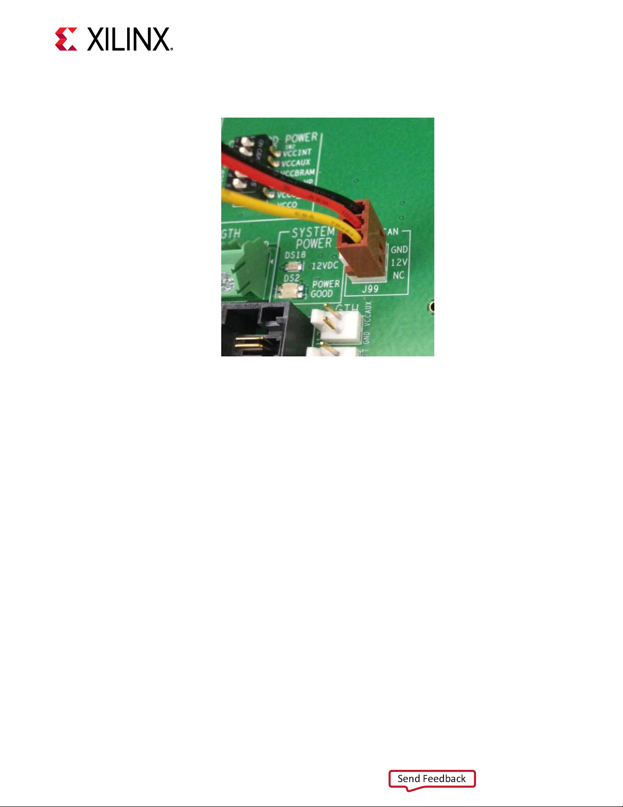
Chapter 1: ZCU1285 Board Features and Operation
Send Feedback
Figure 21: Heat Sink Fan Power Connector J99
UG1348 (v1.0) July 16, 2019 www.xilinx.com
ZCU1285 Board User Guide 55
Page 56

Appendix A: Regulatory and Compliance Information
Send Feedback
Regulatory and Compliance
Information
This product is designed and tested to conform to the European Union direcves and standards
described in this secon.
For Technical Support, open a Support Service Request.
Appendix A
CE Information
CE Directives
2006/95/EC, Low Voltage Direcve (LVD)
2004/108/EC, Electromagnec Compability (EMC) Direcve
CE Standards
EN standards are maintained by the European Commiee for Electrotechnical Standardizaon
(CENELEC). IEC standards are maintained by the Internaonal Electrotechnical Commission (IEC).
CE Electromagnetic Compatibility
EN 55022:2010, Informaon Technology Equipment Radio Disturbance Characteriscs – Limits and
Methods of Measurement
EN 55024:2010, Informaon Technology Equipment Immunity Characteriscs – Limits and Methods
of Measurement
This is a Class A product. In a domesc environment, this product can cause radio interference, in
which case the user might be required to take adequate measures.
UG1348 (v1.0) July 16, 2019 www.xilinx.com
ZCU1285 Board User Guide 56
CE Safety
IEC 60950-1:2005, Informaon technology equipment – Safety, Part 1: General requirements
EN 60950-1:2006, Informaon technology equipment – Safety, Part 1: General requirements
Page 57

Compliance Markings
Send Feedback
In August of 2005, the European Union (EU) implemented the EU Waste Electrical
and Electronic Equipment (WEEE) Directive 2002/96/EC and later the WEEE Recast
Directive 2012/19/EU. These directives require Producers of electronic and
electrical equipment (EEE) to manage and finance the collection, reuse, recycling
and to appropriately treat WEEE that the Producer places on the EU market after
August 13, 2005. The goal of this directive is to minimize the volume of electrical
and electronic waste disposal and to encourage re-use and recycling at the end
of life.
Xilinx has met its national obligations to the EU WEEE Directive by registering in
those countries to which Xilinx is an importer. Xilinx has also elected to join WEEE
Compliance Schemes in some countries to help manage customer returns at
end-of-life.
If you have purchased Xilinx-branded electrical or electronic products in the EU
and are intending to discard these products at the end of their useful life, please
do not dispose of them with your other household or municipal waste. Xilinx has
labeled its branded electronic products with the WEEE Symbol to alert our
customers that products bearing this label should not be disposed of in a landfill
or with municipal or household waste in the EU.
Appendix A: Regulatory and Compliance Information
This product complies with Directive 2002/95/EC on the restriction of hazardous
substances (RoHS) in electrical and electronic equipment.
This product complies with CE Directives 2006/95/EC, Low Voltage Directive (LVD)
and 2004/108/EC, Electromagnetic Compatibility (EMC) Directive.
UG1348 (v1.0) July 16, 2019 www.xilinx.com
ZCU1285 Board User Guide 57
Page 58

Default Jumper Settings
Send Feedback
The following table lists the jumpers that must be installed on the ZCU1285 board for proper
operaon. These jumpers must be installed except where specically noted in this user guide.
IMPORTANT! Any jumper not listed in the following table should be le open for normal operaon.
Table 28: Default Jumper Settings
Appendix B: Default Jumper Settings
Appendix B
Reference
Designator
SW2.2 VCCINT Upper left ENABLED
SW2.3 VCCAUX Upper left ENABLED
SW2.4 VCCBRAM Upper left ENABLED
SW2.5 VCCO_HP Upper left ENABLED
SW2.6 VCCO_HD Upper left ENABLED
SW2.7 VCCPINT Upper left ENABLED
SW2.8 VCCPAUX Upper left ENABLED
SW2.9 VCC_PSPLL Upper left ENABLED
SW2.10 VCCO_DDR Upper left ENABLED
SW2.11 VCCO_MIO Upper left ENABLED
SW2.12 VCCINT_AMS Upper left ENABLED
J87 GTY PMBUS CTRL Upper left GND (2-3)
J215 PMBUS CTRL Center Left GND (2-3)
J40 POR_OVERRIDE Center middle GND (2-3)
J121 DUT I2C Upper right GND (2-3) DIS Disabled
J125 SYS I2C Upper right PWR (1-2) EN Enabled
J154 GTY PMBUS ISO Upper right Installed
J8 PMBUS ISO Upper right Installed
J165 PS Mode Pin 0 Upper right GND (2-3) JTAG mode
J166 PS Mode Pin 1 Upper right GND (2-3) JTAG mode
J164 PS Mode Pin 2 Upper right GND (2-3) JTAG mode
J163 PS Mode Pin 3 Upper right GND (2-3) JTAG mode
J275 VTT_HP SOURCE Upper right VTT_HP (1-2)
J216 VTT_HD SOURCE Lower Right VTT_HD (1-2)
J60 APM PMBUS CTRL Center Right Installed
J11 CLK_DIFF_1_P Lower Middle Installed
Name Board Location
Jumper/DIP-Switch
Position
Comments
UG1348 (v1.0) July 16, 2019 www.xilinx.com
ZCU1285 Board User Guide 58
Page 59

Table 28: Default Jumper Settings (cont'd)
Send Feedback
Appendix B: Default Jumper Settings
Reference
Designator
J12 CLK_DIFF_1_N Lower Middle Installed
J13 CLK_DIFF_2_P Lower Middle Installed
J14 CLK_DIFF_2_N Lower Middle Installed
Name Board Location
Jumper/DIP-Switch
Position
Comments
UG1348 (v1.0) July 16, 2019 www.xilinx.com
ZCU1285 Board User Guide 59
Page 60

Appendix C: VITA 57.1 FMC Connector Pinouts
Send Feedback
Appendix C
VITA 57.1 FMC Connector Pinouts
The following table provides a cross-reference of signal names to pin coordinates for the VITA
57.1 FMC high pin count (HPC) connector.
Table 29: FMC HPC Connector Pinout
K J H G F E D C B A
1 VREF_B_M2C GND VREF_A_M2C GND PG_M2C GND PG_C2M GND RES1 GND
2 GND CLK3_M2C_P PRSNT_M2C_L CLK1_M2C_P GND HA01_P_CC GND DP0_C2M_P GND DP1_M2C_P
3 GND CLK3_M2C_N GND CLK1_M2C_N GND HA01_N_CC GND DP0_C2M_N GND DP1_M2C_N
4 CLK2_M2C_P GND CLK0_M2C_P GND HA00_P_CC GND GBTCLK0_M2C_PGND DP9_M2C_P GND
5 CLK2_M2C_N GND CLK0_M2C_N GND HA00_N_CC GND GBTCLK0_M2C_NGND DP9_M2C_N GND
6 GND HA03_P GND LA00_P_CC GND HA05_P GND DP0_M2C_P GND DP2_M2C_P
7 HA02_P HA03_N LA02_P LA00_N_CC HA04_P HA05_N GND DP0_M2C_N GND DP2_M2C_N
8 HA02_N GND LA02_N GND HA04_N GND LA01_P_CC GND DP8_M2C_P GND
9 GND HA07_P GND LA03_P GND HA09_P LA01_N_CC GND DP8_M2C_N GND
10 HA06_P HA07_N LA04_P LA03_N HA08_P HA09_N GND LA06_P GND DP3_M2C_P
11 HA06_N GND LA04_N GND HA08_N GND LA05_P LA06_N GND DP3_M2C_N
12 GND HA11_P GND LA08_P GND HA13_P LA05_N GND DP7_M2C_P GND
13 HA10_P HA11_N LA07_P LA08_N HA12_P HA13_N GND GND DP7_M2C_N GND
14 HA10_N GND LA07_N GND HA12_N GND LA09_P LA10_P GND DP4_M2C_P
15 GND HA14_P GND LA12_P GND HA16_P LA09_N LA10_N GND DP4_M2C_N
16 HA17_P_CC HA14_N LA11_P LA12_N HA15_P HA16_N GND GND DP6_M2C_P GND
17 HA17_N_CC GND LA11_N GND HA15_N GND LA13_P GND DP6_M2C_N GND
18 GND HA18_P GND LA16_P GND HA20_P LA13_N LA14_P GND DP5_M2C_P
19 HA21_P HA18_N LA15_P LA16_N HA19_P HA20_N GND LA14_N GND DP5_M2C_N
20 HA21_N GND LA15_N GND HA19_N GND LA17_P_CC GND GBTCLK1_M2C_PGND
21 GND HA22_P GND LA20_P GND HB03_P LA17_N_CC GND GBTCLK1_M2C_NGND
22 HA23_P HA22_N LA19_P LA20_N HB02_P HB03_N GND LA18_P_CC GND DP1_C2M_P
23 HA23_N GND LA19_N GND HB02_N GND LA23_P LA18_N_CC GND DP1_C2M_N
24 GND HB01_P GND LA22_P GND HB05_P LA23_N GND DP9_C2M_P GND
25 HB00_P_CC HB01_N LA21_P LA22_N HB04_P HB05_N GND GND DP9_C2M_N GND
26 HB00_N_CC GND LA21_N GND HB04_N GND LA26_P LA27_P GND DP2_C2M_P
27 GND HB07_P GND LA25_P GND HB09_P LA26_N LA27_N GND DP2_C2M_N
28 HB06_P_CC HB07_N LA24_P LA25_N HB08_P HB09_N GND GND DP8_C2M_P GND
29 HB06_N_CC GND LA24_N GND HB08_N GND TCK GND DP8_C2M_N GND
30 GND HB11_P GND LA29_P GND HB13_P TDI SCL GND DP3_C2M_P
31 HB10_P HB11_N LA28_P LA29_N HB12_P HB13_N TDO SDA GND DP3_C2M_N
32 HB10_N GND LA28_N GND HB12_N GND 3P3VAUX GND DP7_C2M_P GND
UG1348 (v1.0) July 16, 2019 www.xilinx.com
ZCU1285 Board User Guide 60
Page 61

Appendix C: VITA 57.1 FMC Connector Pinouts
Send Feedback
Table 29: FMC HPC Connector Pinout (cont'd)
K J H G F E D C B A
33 GND HB15_P GND LA31_P GND HB19_P TMS GND DP7_C2M_N GND
34 HB14_P HB15_N LA30_P LA31_N HB16_P HB19_N TRST_L GA0 GND DP4_C2M_P
35 HB14_N GND LA30_N GND HB16_N GND GA1 12P0V GND DP4_C2M_N
36 GND HB18_P GND LA33_P GND HB21_P 3P3V GND DP6_C2M_P GND
37 HB17_P_CC HB18_N LA32_P LA33_N HB20_P HB21_N GND 12P0V DP6_C2M_N GND
38 HB17_N_CC GND LA32_N GND HB20_N GND 3P3V GND GND DP5_C2M_P
39 GND VIO_B_M2C GND VADJ GND VADJ GND 3P3V GND DP5_C2M_N
40 VIO_B_M2C GND VADJ GND VADJ GND 3P3V GND RES0 GND
UG1348 (v1.0) July 16, 2019 www.xilinx.com
ZCU1285 Board User Guide 61
Page 62

Appendix D: Master Constraints File Listing
Send Feedback
Appendix D
Master Constraints File Listing
The Xilinx design constraints (XDC) le template for the ZCU1285 board provides for designs
targeng the Zynq UltraScale+ RFSoC ZCU1285 characterizaon kit. Net names in the listed
constraints correlate with net names on the ZCU1285 board schemac. Idenfy the appropriate
pins and replace the following net names with net names in the user RTL. See the Vivado Design
Suite User Guide: Using Constraints (UG903) for more informaon.
See the boards le on the ZCU1285 Characterizaon Kit documentaon website for the latest
version of the FPGA XDC le.
UG1348 (v1.0) July 16, 2019 www.xilinx.com
ZCU1285 Board User Guide 62
Page 63
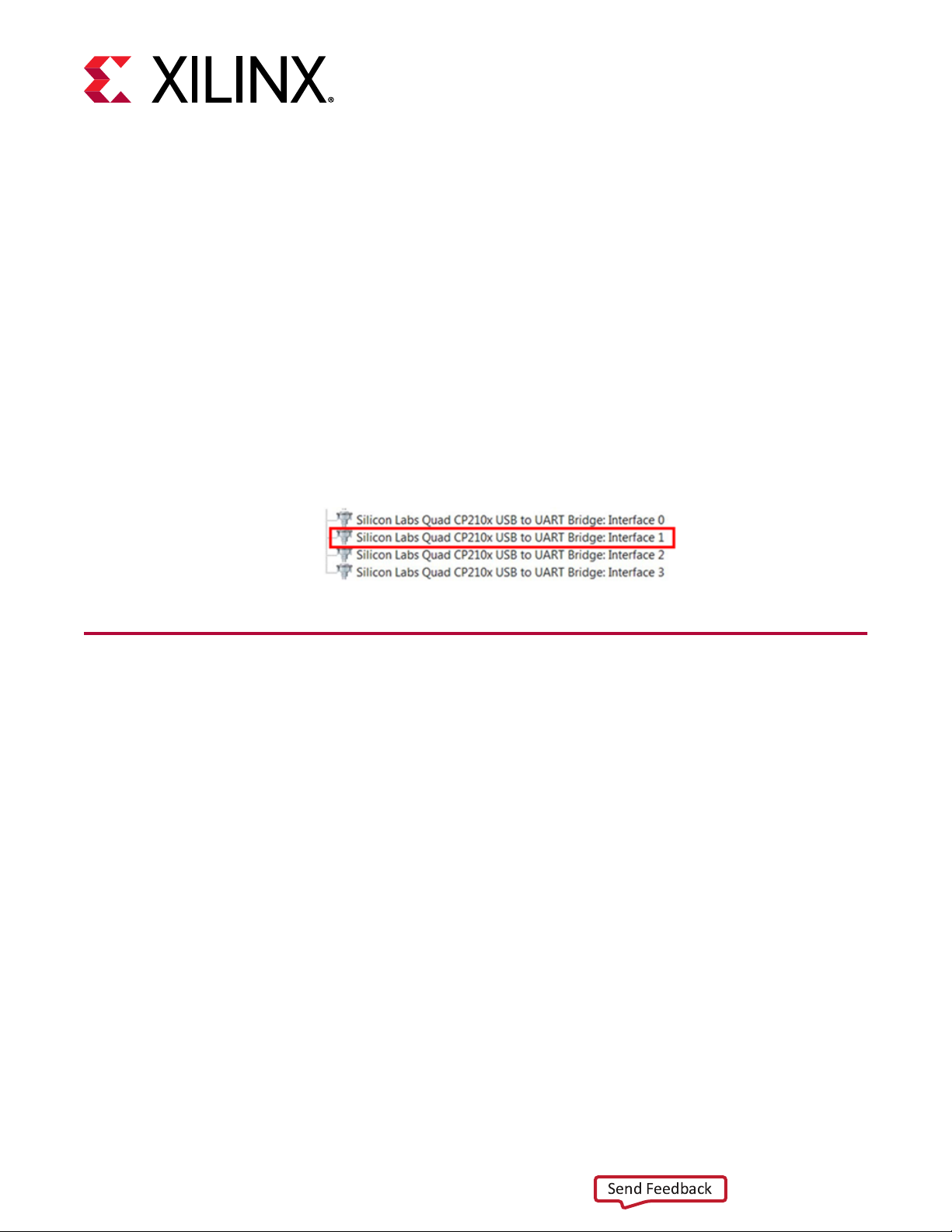
System Controller
Send Feedback
The Xilinx system controller is an applicaon that runs on a Zynq-7000 SoC at power-up on the
ZCU1285 board. The System Controller user interface (SCUI) can be downloaded from the Zynq
UltraScale+ RFSoC ZCU1285 Characterizaon Kit documentaon page. The SCUI le rdf0513-
zcu1285-system-controller-2019-1.zip is associated with this user guide. The SCUI
communicates with the Zynq-7000 SoC using the Interface 1 port of the Silicon Labs USB to
Quad-UART described in the USB to Quad-UART Bridge. See the following gure.
Figure 22: Silicon Labs Interface 1 COM Port
Appendix E
Connecting the System Controller User Interface
Aer starng the SCUI, a window opens with elds for entering informaon about the board (see
the following gure). These values can later be stored into EEPROM in the EEPROM Data tab. If
the EEPROM data has already been stored, only the Board and Revision elds need to be
selected.
UG1348 (v1.0) July 16, 2019 www.xilinx.com
ZCU1285 Board User Guide 63
Page 64

Appendix E: System Controller
Send Feedback
Figure 23: SCUI Board Information Window
Aer entering the board informaon and pressing OK, the main window of the SCUI is displayed
(see the following gure). On the le side of the window is the system controller controls and on
the right side is a log of the operaons.
Figure 24: SCUI Main Window
UG1348 (v1.0) July 16, 2019 www.xilinx.com
ZCU1285 Board User Guide 64
Page 65

Connect a USB A to Micro-B USB cable from the host PC to the ZCU1285 USB/UART connector
Send Feedback
(callout 5, Figure 1-2). In the SCUI click File → Change the System Controller Port. In the Select
the system controller port window, select the COM port associated with Silicon Labs Quad
CP210x USB to UART Bridge: Interface 2, and press OK. The SCUI is now connected to the
ZCU1285 board.
IMPORTANT! Make sure J121 is set to posion (2-3) DUT PMBUS DIS to isolate the DUT PMBUS/I2C signals
and prevent bus contenon. If contenon occurs, the system controller cannot execute commands.
Programmable Clocks Tab
The Clocks tab (see following gure) is used to set the frequency of the SuperClock-2 Module
clock sources (see SuperClock-2 Module) and the SuperClock-RF2 Module clock sources (see
SuperClock-RF2 Module).
Appendix E: System Controller
Figure 25: Clocks Tab
Under the Clocks tab is another row of tabs to select either the SuperClock-2 Module (CLK-101)
or the SuperClock-RF2 Module (CLK-103).
CLK-101 Tab
This secon includes a descripon of the CLK-101 tab opons that are used to control the
SuperClock-2 Module. Arbitrary eld value entries are used to illustrate the operaons. The
CLK-101 tab is shown in the following gure.
Figure 26: CLK-101 Tab
UG1348 (v1.0) July 16, 2019 www.xilinx.com
ZCU1285 Board User Guide 65
Note: For each of the following operaons, several seconds might elapse before the operaon completes.
Page 66

Appendix E: System Controller
Send Feedback
Set CLK-101 Si570 Frequency
In the Set tab, enter the desired Si570 frequency in MHz in the eld next to the Set Si570 User
Frequency buon and press Enter or click the buon (see the following gure). Aer the
frequency is set, the Logging pane shows no errors and prints Finished.
Figure 27: CLK-101 Set Si570 User Frequency
Set CLK-101 Si5368 Frequency
There are two buons in the Set tab that can be used to program the Si5368 clock source: Set
Si5368 Frequency (Auto Select) and Set Si5368 Frequency (Free Running). The free-running
opon uses the onboard XA-XB crystal as the acve clock routed to the Si5368 internal PLL. The
auto select opon uses one of the recovery clocks routed to the SuperClock-2 Module interface
as the acve clock. Enter the desired Si5368 frequency in MHz in the eld next to either the
auto select or free-running buons and press Enter or click the related buon (see the following
gure). Aer the frequency is set, the Logging pane shows no errors and prints Finished.
UG1348 (v1.0) July 16, 2019 www.xilinx.com
ZCU1285 Board User Guide 66
Page 67

Appendix E: System Controller
Send Feedback
Figure 28: CLK-101 Set Si5368 Frequency
Save CLK-101 Boot Frequency to EEPROM
Default boot frequency sengs can be stored in EEPROM, which are programmed into each
clock source at power-up. Enter the desired boot frequencies in the Set Boot Frequency tab and
press Enter to save the boot frequency to EEPROM (see the following gure). Aer the boot
frequencies are set, the Logging pane shows no errors and prints Finished.
Figure 29: CLK-101 Set Boot Frequency Tab
UG1348 (v1.0) July 16, 2019 www.xilinx.com
ZCU1285 Board User Guide 67
Page 68

Appendix E: System Controller
Send Feedback
Restore CLK-101 Boot Frequency from EEPROM
The boot frequencies saved in EEPROM can be restored at any me using the Restore Device
Defaults tab. Click Restore Si570 User to restore the Si570 frequency stored in EEPROM, and
click Restore Si5368 User to restore the Si5368 frequency stored in EEPROM (see the following
gure).
Figure 30: CLK-101 Restore Device Defaults Tab
View Last Set CLK-101 Frequencies
The last frequencies that were wrien to the CLK-101 Module can be viewed using the Last Set
tab. Click Read Si570 User Frequency to view the Si570 frequency and Last Set Si5368 User
Frequency to view the Si5368 frequency (see the following gure).
Figure 31: CLK-101 Last Set Tab
UG1348 (v1.0) July 16, 2019 www.xilinx.com
ZCU1285 Board User Guide 68
Page 69

Appendix E: System Controller
Send Feedback
CLK-103 Tab
This secon includes a descripon of the CLK-103 tab opons used to control the SuperClock-
RF2 Module. Arbitrary eld value entries are used to illustrate the operaons. The CLK-103 tab
is shown in the following gure.
Figure 32: CLK-103 Tab
The SCUI is packaged with a set of clock les that contain register values for preset frequencies
used by the SuperClock-RF2 clock sources. Each clock source has its own folder where the clock
les are stored. The folders are located in BoardUI\tests\ZCU1285\clockFiles (see the
following gure).
Note: Do not move or rename any of the folders because the SCUI relies on the directory structure to nd
the clock les.
Figure 33: CLK-103 Clock Files
Note: For each of the following operaons, several seconds might elapse before the operaon completes.
Set CLK-103 LMK04208 (General Purpose Clock) Frequency
In the Set tab, enter the full le name of the clock le with the desired LMK04208 frequency in
the eld next to the Type le name in the clockFiles/lmk04208 folder and press Enter or click the
Set LMK04208 Frequency buon (see following the gure). Aer the frequency is set, the
Logging pane shows no errors and prints Finished.
UG1348 (v1.0) July 16, 2019 www.xilinx.com
ZCU1285 Board User Guide 69
Page 70

Appendix E: System Controller
Send Feedback
Figure 34: CLK-103 Set LMK04208 Frequency
Aer entering a clock le, the current sengs and frequencies are listed to the right of the
relevant elds. To change the output divisors of an LMK04208 clock source, enter the new
divisor in the Output Divisor eld and press Enter. To disable or enable an output, use the
Output PwrDwn eld. A "0" enables the output and a "1" disables it.
Set CLK-103 LMX2592 PLL A, B, and C Frequency
Enter the full le name of the clock le with the desired frequency for PLL A in the eld next to
the Type le name in the clockFiles/lmx2592a folder and press Enter or click the Set
LMX2592_A Frequency buon (see following the gure). The same can be done for PLL B and C
in the next two elds down. Be sure to enter the exact le names from the associated folders.
Aer the frequency is set, the Logging pane shows no errors and prints Finished.
UG1348 (v1.0) July 16, 2019 www.xilinx.com
ZCU1285 Board User Guide 70
Page 71

Appendix E: System Controller
Send Feedback
Figure 35: CLK-103 Set LMX2592 Frequency
Save CLK-103 Boot Frequency to EEPROM
Default boot frequency sengs can be stored in EEPROM, which are programmed into each
clock source at power-up. In the Set Boot Frequency tab, enter the full name of the clock les for
the desired boot frequencies in each le name eld. In addion, LMK04208 output divisors and
enable/disable sengs can also be entered and stored. Aer clock les and values are entered,
click the related set boot frequency buon to store (see the following gure). Aer the boot
frequencies are set, the Logging pane shows no errors and prints Finished.
UG1348 (v1.0) July 16, 2019 www.xilinx.com
ZCU1285 Board User Guide 71
Page 72

Appendix E: System Controller
Send Feedback
Figure 36: CLK-103 Set Boot Frequency Tab
UG1348 (v1.0) July 16, 2019 www.xilinx.com
ZCU1285 Board User Guide 72
To view the boot frequency saved in EEPROM, click the related get boot frequency buon in the
Set Boot Frequency tab.
View Last Set CLK-103 Frequencies
The last frequencies that were wrien to the CLK-103 Module can be viewed using the Last Set
tab. Click the relevant last set buon to view the last frequency wrien to the PLL by the SCUI
(see the following gure).
Page 73

Figure 37: CLK-103 Last Set Tab
Send Feedback
Appendix E: System Controller
Reset CLK-103 Clocks
The SuperClock-RF2 clocks can be reset from the Reset Device For New Input tab. Click the
corresponding reset buon to restore the PLL registers to the default values (see the following
gure).
Figure 38: CLK-103 Reset Device For New Input Tab
Power Tab
UG1348 (v1.0) July 16, 2019 www.xilinx.com
ZCU1285 Board User Guide 73
The SCUI can read the onboard INA226 power rail measurements for each of the power rails
listed in the following table. The measurements can be read once or scanned connuously.
Page 74
Table 30: Monitored Power Rails
Send Feedback
RFSoC logic and processor
GTY transceiver
PS-GTR transceiver
Appendix E: System Controller
Power Rail
VCCINT
VCCBRAM
VCCAUX
VCCO_HP
VCCO_HD
VCCPINT
VCCPAUX
VCC_PSPLL
VCCO_DDR
VCCO_MIO
VCCINT_AMS
MGTAVCC
MGTAVTT
MGTVCCAUX
MGTRAVCC
MGTRAVTT
Read a Single Power Rail
To read a single power rail measurement, click the corresponding buon with the power rail
name on it. The power, voltage, and current measurements appear to the right of the buon (see
the following gure).
UG1348 (v1.0) July 16, 2019 www.xilinx.com
ZCU1285 Board User Guide 74
Page 75
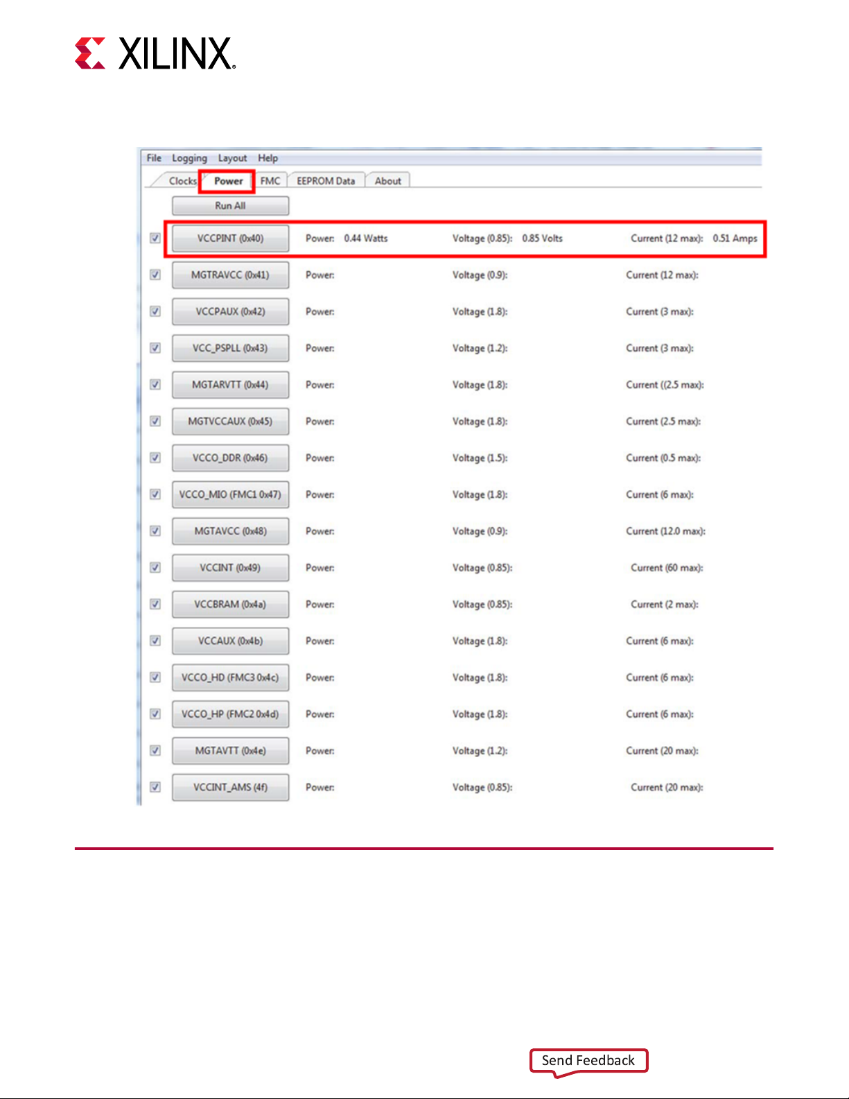
Figure 39: Read a Single Power Rail
Send Feedback
Appendix E: System Controller
Read Multiple Power Rails
UG1348 (v1.0) July 16, 2019 www.xilinx.com
ZCU1285 Board User Guide 75
To read mulple power rail measurements at once, check the box to the le of each power rail
buon and click Run All (see the following gure).
Page 76

Figure 40: Read Multiple Power Rails
Send Feedback
Appendix E: System Controller
Read Power Rails Continuously
UG1348 (v1.0) July 16, 2019 www.xilinx.com
ZCU1285 Board User Guide 76
To connuously read power rails, use the Buon Funconality opons at the boom of the SCUI.
Select either the Run Connuously or Run x mes, then click the power rail buon to read the
measurements. To stop the reading, click Terminate Running Operaons (see the following
gure).
Page 77
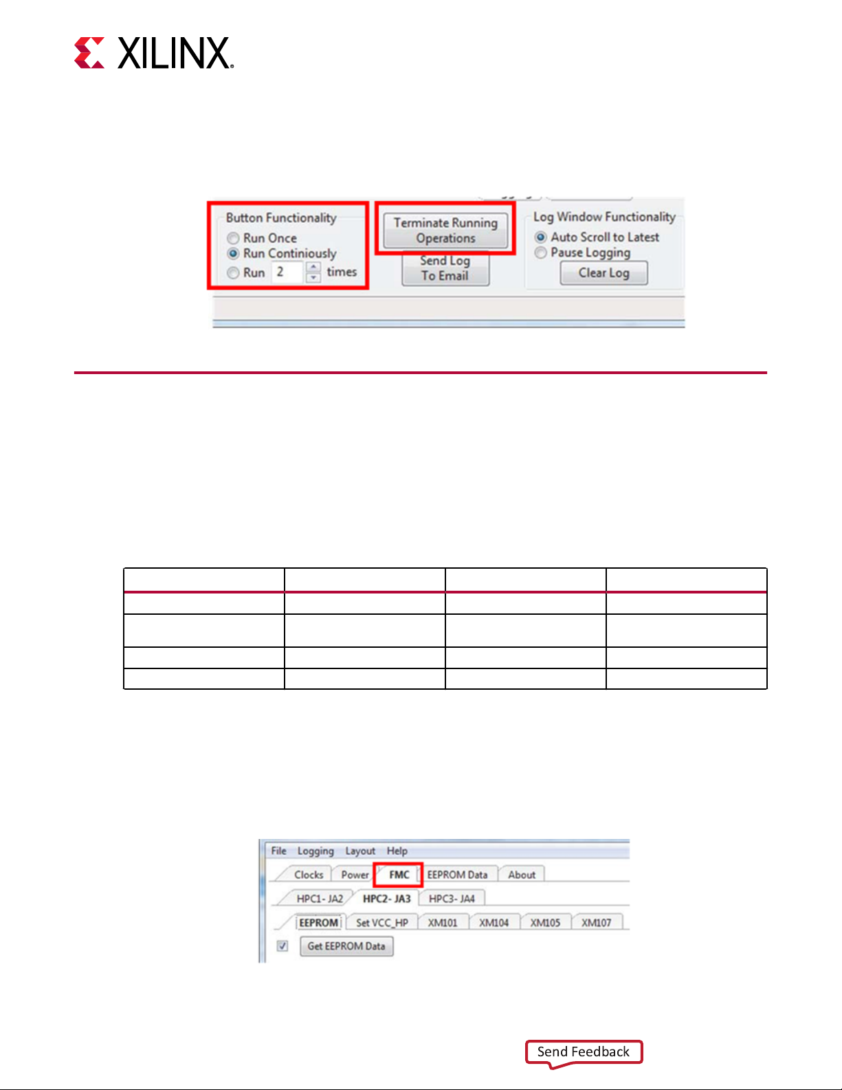
Note: The Buon Funconality opons apply to all buons in the System Controller pane, not just the
Send Feedback
Power tab. Be sure to switch back to Run Once when using other tabs in the SCUI.
FMC Tab
Appendix E: System Controller
Figure 41: Read Power Rails Continuously
The ZCU1285 board provides two FPGA mezzanine card (FMC) ANSI/VITA 57.1 expansion
interfaces, JA3 and JA4 (callout 53 and 54, Figure 2: Board Component Locaons). The following
table shows the FMC cards supported by the System Controller and the programmable clock
resources on each card.
Table 31: FMC Card Clock Sources
Xilinx FMC Card Description Clock Source #1 Clock Source #2
XM101 LVDS QSE card Si570 SI570
XM104 Serial transceiver
connectivity card
XM105 Debug card Si570 N/A
XM107 Loopback card Si570 N/A
Notes:
1. These FMC cards are not included in the ZCU1285 kit.
Si570 Si5368
The FMC tab has opons for viewing FMC card EEPROM data, changing the VADJ voltage for
each FMC interface, and programming clock sources (see the following gure).
Figure 42: FMC Tab
UG1348 (v1.0) July 16, 2019 www.xilinx.com
ZCU1285 Board User Guide 77
Page 78
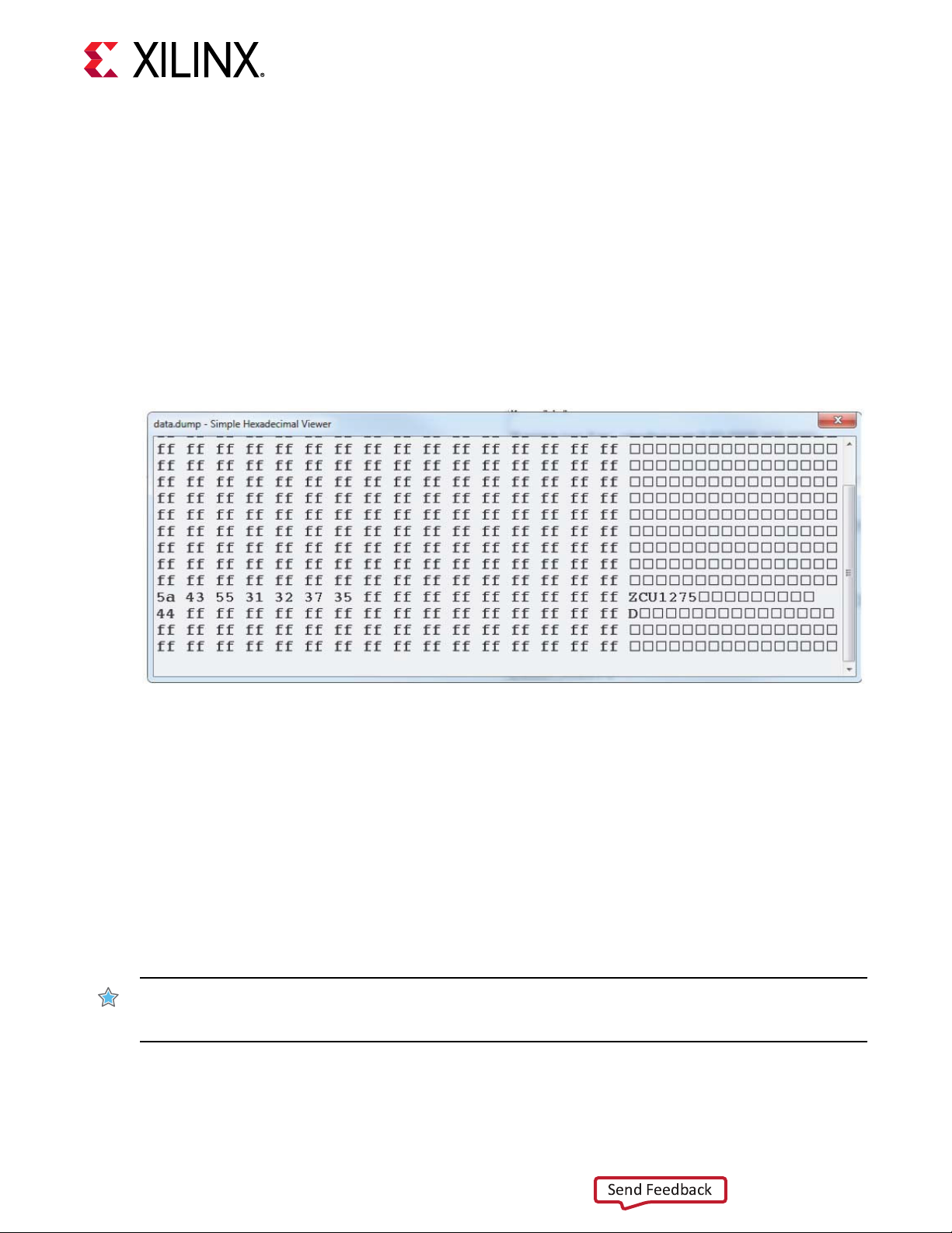
Appendix E: System Controller
Send Feedback
View FMC EEPROM Data
All FMC mezzanine cards host an I2C EEPROM that can be read out through the FMC menu. A
hexadecimal display and a formaed version of the FMC EEPROM data are provided through the
FMC menu. The VITA 57.1 standard idenes the data elds of the intelligent plaorm
management interface (IPMI) specicaon used for the FMC EEPROM.
Select the FMC interface tab with the target FMC card, and then select the EEPROM tab and
click Get EEPROM Data. A window appears displaying the contents of the EEPROM. The
example shown in the following gure is for an XM107 card connected to JA3.
Figure 43: Get EEPROM Data Window
UG1348 (v1.0) July 16, 2019 www.xilinx.com
ZCU1285 Board User Guide 78
Set FMC VADJ
Each FMC interface connects to a set of I/O banks on the RFSoC. The RFSoC bank voltage is
connected to VADJ on the FMC interface to allow the FMC card to track the bank voltage that is
connected to it. The system controller can change the bank voltage that is connected to each
FMC interface. JA3 is connected to VCCO_HP bank I/O pins and JA4 is connected to VCCO_HD
bank I/O pins.
Select the FMC interface tab with the target FMC card. Select the Set VCC_HP or Set VCC_HD
tab, depending on the interface. Click the buon with the desired bank voltage (see the following
gure).
IMPORTANT!
interface. Conrm that any other I/Os being used on the ZCU1285 board are compable with the new bank
voltage.
Note: Power cycling ZCU1285 reverts all bank voltage changes back to the default voltage levels.
Changing the bank voltage aects all banks connected to that bank voltage, not just the FMC
Page 79
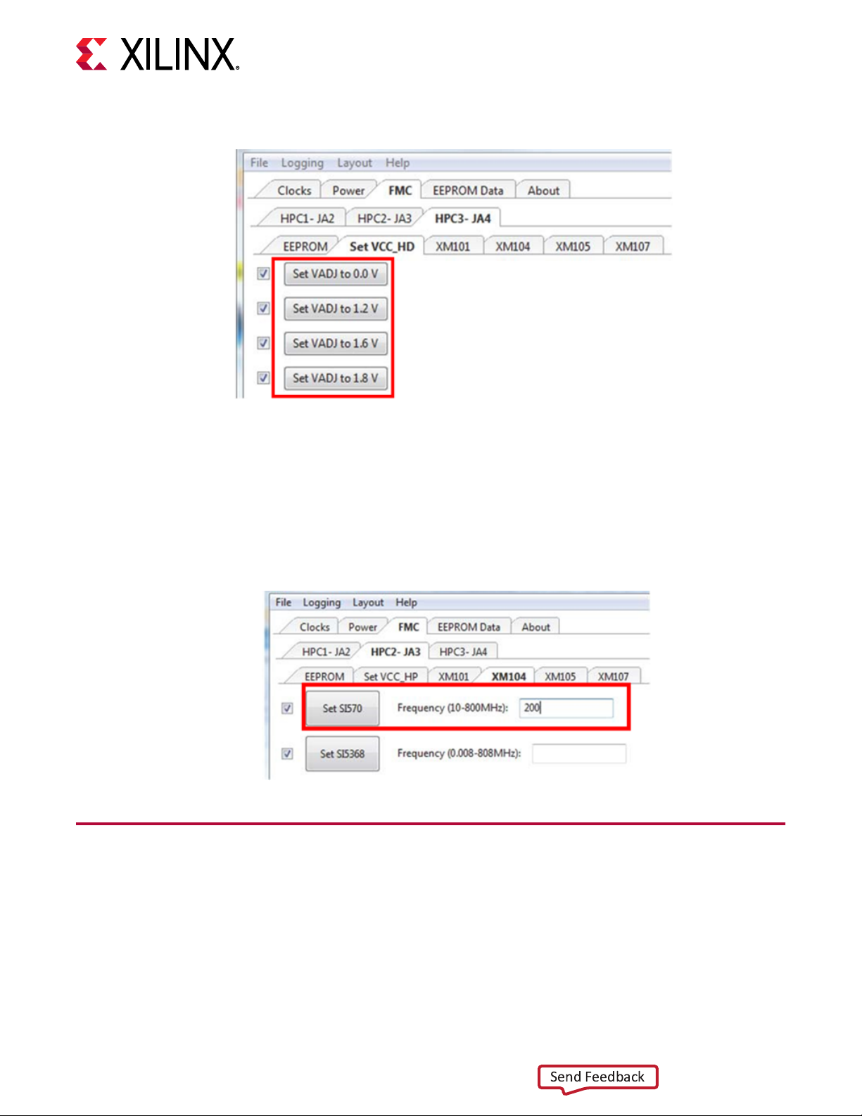
Set FMC Clocks
Send Feedback
Appendix E: System Controller
Figure 44: Set VADJ
Select the FMC interface tab with the target FMC card, and then select the tab with the FMC
card part number (XM101, XM104, XM105, or XM107). Each tab has opons to set the clocks
on available clock sources. Enter the frequency in MHz and click Set SI570 or Set SI5368 to
program the clock. The example shown in the following gure sets the SI570 clock to 200 MHz
on an XM104 card connected to JA3.
EEPROM Data Tab
UG1348 (v1.0) July 16, 2019 www.xilinx.com
ZCU1285 Board User Guide 79
The ZCU1285 System Controller includes an EEPROM that is used to store board informaon.
The informaon entered into the Board Informaon window that appears when the SCUI is
launched (see the SCUI Board Informaon Window in Connecng the System Controller User
Interface) can be stored to the EEPROM using the EEPROM Data tab. The EEPROM data can
also be read using this tab (see the following gure).
Page 80

Figure 45: EEPROM Data
Send Feedback
Appendix E: System Controller
Write Board EEPROM Data
UG1348 (v1.0) July 16, 2019 www.xilinx.com
ZCU1285 Board User Guide 80
To write EEPROM data, use the Set buons highlighted in the following gure.
Page 81
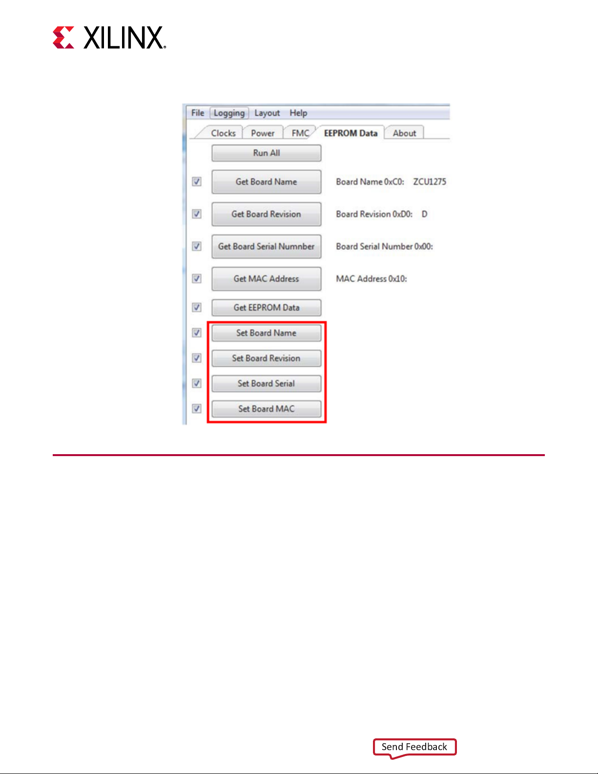
Figure 46: Set EEPROM Data
Send Feedback
Appendix E: System Controller
Read Board EEPROM Data
UG1348 (v1.0) July 16, 2019 www.xilinx.com
ZCU1285 Board User Guide 81
To read EEPROM data, use the Get buons highlighted in the following gure.
Page 82

Figure 47: Get EEPROM Data
Send Feedback
Appendix E: System Controller
The Get EEPROM Data buon opens a window displaying the full contents of the EEPROM
memory (see the following gure).
Figure 48: Get EEPROM Data Window
UG1348 (v1.0) July 16, 2019 www.xilinx.com
ZCU1285 Board User Guide 82
Page 83

Appendix F
Send Feedback
Additional Resources and Legal
Notices
Xilinx Resources
For support resources such as Answers, Documentaon, Downloads, and Forums, see Xilinx
Support.
Documentation Navigator and Design Hubs
Xilinx® Documentaon Navigator (DocNav) provides access to Xilinx documents, videos, and
support resources, which you can lter and search to nd informaon. To open DocNav:
• From the Vivado® IDE, select Help → Documentaon and Tutorials.
• On Windows, select Start → All Programs → Xilinx Design Tools → DocNav.
• At the Linux command prompt, enter docnav.
Xilinx Design Hubs provide links to documentaon organized by design tasks and other topics,
which you can use to learn key concepts and address frequently asked quesons. To access the
Design Hubs:
• In DocNav, click the Design Hubs View tab.
• On the Xilinx website, see the Design Hubs page.
Note: For more informaon on DocNav, see the Documentaon Navigator page on the Xilinx website.
UG1348 (v1.0) July 16, 2019 www.xilinx.com
ZCU1285 Board User Guide 83
Page 84

References
Send Feedback
The most up to date informaon related to the ZCU1285 board and its documentaon is
available on the following websites.
ZCU1285 Characterizaon Kit
Zynq UltraScale+ Characterizaon Kit — Master Answer Record 72434
These documents provide supplemental material useful with this guide:
1. UltraScale Architecture and Product Data Sheet: Overview (DS890)
2. UltraScale Architecture System Monitor User Guide (UG580)
3. Vivado Design Suite User Guide: Using Constraints (UG903)
4. HW-CLK-101-SCLK2 SuperClock-2 Module User Guide (UG770)
Appendix F: Additional Resources and Legal Notices
5. For addional documents associated with Xilinx devices, design tools, intellectual property,
boards, and kits see the Xilinx documentaon website.
These websites provide supplemental material useful with this guide:
6. Informaon about the power system components used in the ZCU1285 board is available
from the Maxim Integrated website at hp://www.maximintegrated.com/en/products/
power/intune
7. Renesas Power Management
8. Texas Instruments
9. Samtec, Inc. Bulls Eye interace
Please Read: Important Legal Notices
The informaon disclosed to you hereunder (the "Materials") is provided solely for the selecon
and use of Xilinx products. To the maximum extent permied by applicable law: (1) Materials are
made available "AS IS" and with all faults, Xilinx hereby DISCLAIMS ALL WARRANTIES AND
CONDITIONS, EXPRESS, IMPLIED, OR STATUTORY, INCLUDING BUT NOT LIMITED TO
WARRANTIES OF MERCHANTABILITY, NON-INFRINGEMENT, OR FITNESS FOR ANY
PARTICULAR PURPOSE; and (2) Xilinx shall not be liable (whether in contract or tort, including
negligence, or under any other theory of liability) for any loss or damage of any kind or nature
related to, arising under, or in connecon with, the Materials (including your use of the
Materials), including for any direct, indirect, special, incidental, or consequenal loss or damage
(including loss of data, prots, goodwill, or any type of loss or damage suered as a result of any
acon brought by a third party) even if such damage or loss was reasonably foreseeable or Xilinx
UG1348 (v1.0) July 16, 2019 www.xilinx.com
ZCU1285 Board User Guide 84
Page 85

Appendix F: Additional Resources and Legal Notices
Send Feedback
had been advised of the possibility of the same. Xilinx assumes no obligaon to correct any
errors contained in the Materials or to nofy you of updates to the Materials or to product
specicaons. You may not reproduce, modify, distribute, or publicly display the Materials
without prior wrien consent. Certain products are subject to the terms and condions of
Xilinx's limited warranty, please refer to Xilinx's Terms of Sale which can be viewed at hps://
www.xilinx.com/legal.htm#tos; IP cores may be subject to warranty and support terms contained
in a license issued to you by Xilinx. Xilinx products are not designed or intended to be fail-safe or
for use in any applicaon requiring fail-safe performance; you assume sole risk and liability for
use of Xilinx products in such crical applicaons, please refer to Xilinx's Terms of Sale which can
be viewed at hps://www.xilinx.com/legal.htm#tos.
AUTOMOTIVE APPLICATIONS DISCLAIMER
AUTOMOTIVE PRODUCTS (IDENTIFIED AS "XA" IN THE PART NUMBER) ARE NOT
WARRANTED FOR USE IN THE DEPLOYMENT OF AIRBAGS OR FOR USE IN APPLICATIONS
THAT AFFECT CONTROL OF A VEHICLE ("SAFETY APPLICATION") UNLESS THERE IS A
SAFETY CONCEPT OR REDUNDANCY FEATURE CONSISTENT WITH THE ISO 26262
AUTOMOTIVE SAFETY STANDARD ("SAFETY DESIGN"). CUSTOMER SHALL, PRIOR TO USING
OR DISTRIBUTING ANY SYSTEMS THAT INCORPORATE PRODUCTS, THOROUGHLY TEST
SUCH SYSTEMS FOR SAFETY PURPOSES. USE OF PRODUCTS IN A SAFETY APPLICATION
WITHOUT A SAFETY DESIGN IS FULLY AT THE RISK OF CUSTOMER, SUBJECT ONLY TO
APPLICABLE LAWS AND REGULATIONS GOVERNING LIMITATIONS ON PRODUCT
LIABILITY.
Copyright
© Copyright 2019 Xilinx, Inc. Xilinx, the Xilinx logo, Alveo, Arx, Kintex, Spartan, Versal, Virtex,
Vivado, Zynq, and other designated brands included herein are trademarks of Xilinx in the United
States and other countries.PCI, PCIe, and PCI Express are trademarks of PCI-SIG and used under
license. All other trademarks are the property of their respecve owners.
UG1348 (v1.0) July 16, 2019 www.xilinx.com
ZCU1285 Board User Guide 85
 Loading...