

Page 1

ZCU102 Evaluation
Board
User Guide
UG1182 (v1.2) March 20, 2017
Page 2
Revision History
Send Feedback
The following table shows the revision history for this document.
Date Version Revision
03/20/2017 1.2
11/16/2016 1.1
05/11/2016 1.0
Added notes to Dimensions in Chapter 1. Updated SW6 default switch setting in
Table 2-2 and SD configuration setting in Table 2-4. Clarified SW6[4:1] boot mode pin
settings under Quad-SPI and SD in Chapter 2. Changed “DDR SODIMM Memory J1”
heading to “DDR Component Memory” in Table 3-4. Changed PS_REF_CLK frequency
from 33 MHz to 33.33 MHz in Table 3-12. Changed “UART2_RTS_O_B” to
“UART2_CTS_O_B” in Table 3-16. Replaced Figure 3-16. Changed “QSPI119 (LWR),
U120 (UPR)” heading to “MSP430 U41” in Table 3-17. Clarified references to
Figure 3-17 in Table 3-19 and Table 3-20. Added addresses to titles in Table 3-21 and
Table 3-22 and headings in Table 3-23 and Table 3-24. Changed “22” to “L22” in
Table 3-28. Updated GTH connectivity for Quad 128, Quad 228, Quad 229, and
Quad 23 under GTH Transceivers in Chapter 3. Updated bank assignments in
Figure 3-35. Added callout 44 to Switches in Chapter 3. Updated Xilinx websites in
Appendix D, Additional Resources and Legal Notices.
Updated device part number from XCZU9EG-2FFVB1156 to XCZU9EG-2FFVB1156I
throughout document. Updated board photos (Figure 2-1 and Figure 2-1) to rev 1.0.
Updated Table 2-1 and Table 2-3. Updated Chapter 3, Component Descriptions.
Updated Appendix B, Master Constraints File Listing.
Initial Xilinx release - limited distribution.
ZCU102 Evaluation Board User Guide www.xilinx.com 2
UG1182 (v1.2) March 20, 2017
Page 3

Table of Contents
Send Feedback
Revision History . . . . . . . . . . . . . . . . . . . . . . . . . . . . . . . . . . . . . . . . . . . . . . . . . . . . . . . . . . . . . . . . . . . . 2
Chapter 1: Introduction
Overview . . . . . . . . . . . . . . . . . . . . . . . . . . . . . . . . . . . . . . . . . . . . . . . . . . . . . . . . . . . . . . . . . . . . . . . . 6
Block Diagram . . . . . . . . . . . . . . . . . . . . . . . . . . . . . . . . . . . . . . . . . . . . . . . . . . . . . . . . . . . . . . . . . . . . 7
Board Features . . . . . . . . . . . . . . . . . . . . . . . . . . . . . . . . . . . . . . . . . . . . . . . . . . . . . . . . . . . . . . . . . . . . 8
Board Specifications . . . . . . . . . . . . . . . . . . . . . . . . . . . . . . . . . . . . . . . . . . . . . . . . . . . . . . . . . . . . . . 10
Dimensions . . . . . . . . . . . . . . . . . . . . . . . . . . . . . . . . . . . . . . . . . . . . . . . . . . . . . . . . . . . . . . . . . . . . . . . . . . . . . .10
Environmental . . . . . . . . . . . . . . . . . . . . . . . . . . . . . . . . . . . . . . . . . . . . . . . . . . . . . . . . . . . . . . . . . . . . . . . . . . . .10
Operating Voltage . . . . . . . . . . . . . . . . . . . . . . . . . . . . . . . . . . . . . . . . . . . . . . . . . . . . . . . . . . . . . . . . . . . . . . . . .10
Chapter 2: Board Setup and Configuration
Board Component Location. . . . . . . . . . . . . . . . . . . . . . . . . . . . . . . . . . . . . . . . . . . . . . . . . . . . . . . . . 11
Default Switch and Jumper Settings . . . . . . . . . . . . . . . . . . . . . . . . . . . . . . . . . . . . . . . . . . . . . . . . . . 15
Switches . . . . . . . . . . . . . . . . . . . . . . . . . . . . . . . . . . . . . . . . . . . . . . . . . . . . . . . . . . . . . . . . . . . . . . . . . . . . . . . . .16
Jumpers . . . . . . . . . . . . . . . . . . . . . . . . . . . . . . . . . . . . . . . . . . . . . . . . . . . . . . . . . . . . . . . . . . . . . . . . . . . . . . . . .16
MPSoC Device Configuration . . . . . . . . . . . . . . . . . . . . . . . . . . . . . . . . . . . . . . . . . . . . . . . . . . . . . . . 19
Chapter 3: Board Component Descriptions
Overview . . . . . . . . . . . . . . . . . . . . . . . . . . . . . . . . . . . . . . . . . . . . . . . . . . . . . . . . . . . . . . . . . . . . . . . 20
Component Descriptions . . . . . . . . . . . . . . . . . . . . . . . . . . . . . . . . . . . . . . . . . . . . . . . . . . . . . . . . . . . 20
Zynq UltraScale XCZU9EG MPSoC . . . . . . . . . . . . . . . . . . . . . . . . . . . . . . . . . . . . . . . . . . . . . . . . . . . . . . . . . . . .20
PS-Side: DDR4 SODIMM Socket . . . . . . . . . . . . . . . . . . . . . . . . . . . . . . . . . . . . . . . . . . . . . . . . . . . . . . . . . . . . . .24
DDR4 Component Memory . . . . . . . . . . . . . . . . . . . . . . . . . . . . . . . . . . . . . . . . . . . . . . . . . . . . . . . . . . . . . . . . .29
PSMIO . . . . . . . . . . . . . . . . . . . . . . . . . . . . . . . . . . . . . . . . . . . . . . . . . . . . . . . . . . . . . . . . . . . . . . . . . . . . . . . . . . .32
Quad-SPI Flash Memory (MIO 0–12) . . . . . . . . . . . . . . . . . . . . . . . . . . . . . . . . . . . . . . . . . . . . . . . . . . . . . . . . . .33
USB 3.0 Transceiver and USB 2.0 ULPI PHY . . . . . . . . . . . . . . . . . . . . . . . . . . . . . . . . . . . . . . . . . . . . . . . . . . . . .34
SD Card Interface . . . . . . . . . . . . . . . . . . . . . . . . . . . . . . . . . . . . . . . . . . . . . . . . . . . . . . . . . . . . . . . . . . . . . . . . . .37
Programmable Logic JTAG Programming Options . . . . . . . . . . . . . . . . . . . . . . . . . . . . . . . . . . . . . . . . . . . . . . .40
EMIO ARM Trace Port . . . . . . . . . . . . . . . . . . . . . . . . . . . . . . . . . . . . . . . . . . . . . . . . . . . . . . . . . . . . . . . . . . . . . .41
Clock Generation . . . . . . . . . . . . . . . . . . . . . . . . . . . . . . . . . . . . . . . . . . . . . . . . . . . . . . . . . . . . . . . . . . . . . . . . . .43
GEM3 Ethernet (MIO 64-77) . . . . . . . . . . . . . . . . . . . . . . . . . . . . . . . . . . . . . . . . . . . . . . . . . . . . . . . . . . . . . . . .48
10/100/1000 MHz Tri-Speed Ethernet PHY . . . . . . . . . . . . . . . . . . . . . . . . . . . . . . . . . . . . . . . . . . . . . . . . . . . .49
CP2108 USB UART Interface . . . . . . . . . . . . . . . . . . . . . . . . . . . . . . . . . . . . . . . . . . . . . . . . . . . . . . . . . . . . . . . . .51
GPIO (MIO 13, 38) . . . . . . . . . . . . . . . . . . . . . . . . . . . . . . . . . . . . . . . . . . . . . . . . . . . . . . . . . . . . . . . . . . . . . . . . .53
I2C0 (MIO 14-15) . . . . . . . . . . . . . . . . . . . . . . . . . . . . . . . . . . . . . . . . . . . . . . . . . . . . . . . . . . . . . . . . . . . . . . . . . .54
I2C1 (MIO 16-17) . . . . . . . . . . . . . . . . . . . . . . . . . . . . . . . . . . . . . . . . . . . . . . . . . . . . . . . . . . . . . . . . . . . . . . . . . .58
UART0 (MIO 18-19) . . . . . . . . . . . . . . . . . . . . . . . . . . . . . . . . . . . . . . . . . . . . . . . . . . . . . . . . . . . . . . . . . . . . . . . .60
UART1 (MIO 20-21) . . . . . . . . . . . . . . . . . . . . . . . . . . . . . . . . . . . . . . . . . . . . . . . . . . . . . . . . . . . . . . . . . . . . . . . .60
ZCU102 Evaluation Board User Guide www.xilinx.com 3
UG1182 (v1.2) March 20, 2017
Page 4

GPIO (MIO 22-23) . . . . . . . . . . . . . . . . . . . . . . . . . . . . . . . . . . . . . . . . . . . . . . . . . . . . . . . . . . . . . . . . . . . . . . . . .61
Send Feedback
CAN1 (MIO 24-25) . . . . . . . . . . . . . . . . . . . . . . . . . . . . . . . . . . . . . . . . . . . . . . . . . . . . . . . . . . . . . . . . . . . . . . . . .61
PMU GPI (MIO 26) . . . . . . . . . . . . . . . . . . . . . . . . . . . . . . . . . . . . . . . . . . . . . . . . . . . . . . . . . . . . . . . . . . . . . . . . .62
DPAUX (MIO 27-30) . . . . . . . . . . . . . . . . . . . . . . . . . . . . . . . . . . . . . . . . . . . . . . . . . . . . . . . . . . . . . . . . . . . . . . . .62
PCIe Reset (MIO 31) . . . . . . . . . . . . . . . . . . . . . . . . . . . . . . . . . . . . . . . . . . . . . . . . . . . . . . . . . . . . . . . . . . . . . . .64
PMU GPO (MIO 32-37) . . . . . . . . . . . . . . . . . . . . . . . . . . . . . . . . . . . . . . . . . . . . . . . . . . . . . . . . . . . . . . . . . . . . .64
HDMI Video Output. . . . . . . . . . . . . . . . . . . . . . . . . . . . . . . . . . . . . . . . . . . . . . . . . . . . . . . . . . . . . . . . . . . . . . . .64
HDMI Clock Recovery . . . . . . . . . . . . . . . . . . . . . . . . . . . . . . . . . . . . . . . . . . . . . . . . . . . . . . . . . . . . . . . . . . . . . .67
SFP/SFP+ Connector . . . . . . . . . . . . . . . . . . . . . . . . . . . . . . . . . . . . . . . . . . . . . . . . . . . . . . . . . . . . . . . . . . . . . . .68
SFP/SFP+ Clock Recovery . . . . . . . . . . . . . . . . . . . . . . . . . . . . . . . . . . . . . . . . . . . . . . . . . . . . . . . . . . . . . . . . . . .70
User PMOD GPIO Headers . . . . . . . . . . . . . . . . . . . . . . . . . . . . . . . . . . . . . . . . . . . . . . . . . . . . . . . . . . . . . . . . . .71
Prototype Header . . . . . . . . . . . . . . . . . . . . . . . . . . . . . . . . . . . . . . . . . . . . . . . . . . . . . . . . . . . . . . . . . . . . . . . . .72
User I2C0 Receptacle . . . . . . . . . . . . . . . . . . . . . . . . . . . . . . . . . . . . . . . . . . . . . . . . . . . . . . . . . . . . . . . . . . . . . .74
User I/O . . . . . . . . . . . . . . . . . . . . . . . . . . . . . . . . . . . . . . . . . . . . . . . . . . . . . . . . . . . . . . . . . . . . . . . . . . . . . . . . .74
Power and Status LEDs . . . . . . . . . . . . . . . . . . . . . . . . . . . . . . . . . . . . . . . . . . . . . . . . . . . . . . . . . . . . . . . . . . . . .77
GTH Transceivers . . . . . . . . . . . . . . . . . . . . . . . . . . . . . . . . . . . . . . . . . . . . . . . . . . . . . . . . . . . . . . . . . . . . . . . . . .79
PS-Side: GTR Transceivers. . . . . . . . . . . . . . . . . . . . . . . . . . . . . . . . . . . . . . . . . . . . . . . . . . . . . . . . . . . . . . . . . . .89
PCIe (MIO 31) . . . . . . . . . . . . . . . . . . . . . . . . . . . . . . . . . . . . . . . . . . . . . . . . . . . . . . . . . . . . . . . . . . . . . . . . . . . . .92
PCI Express Root Port Slot . . . . . . . . . . . . . . . . . . . . . . . . . . . . . . . . . . . . . . . . . . . . . . . . . . . . . . . . . . . . . . . . . .92
FPGA Mezzanine Card Interface . . . . . . . . . . . . . . . . . . . . . . . . . . . . . . . . . . . . . . . . . . . . . . . . . . . . . . . . . . . . . .93
FMC HPC0 Connector J5 . . . . . . . . . . . . . . . . . . . . . . . . . . . . . . . . . . . . . . . . . . . . . . . . . . . . . . . . . . . . . . . . . . . .93
FMC HPC1 Connector J4 . . . . . . . . . . . . . . . . . . . . . . . . . . . . . . . . . . . . . . . . . . . . . . . . . . . . . . . . . . . . . . . . . . . .98
Cooling Fan Connector . . . . . . . . . . . . . . . . . . . . . . . . . . . . . . . . . . . . . . . . . . . . . . . . . . . . . . . . . . . . . . . . . . . .104
VADJ_FMC Power Rail . . . . . . . . . . . . . . . . . . . . . . . . . . . . . . . . . . . . . . . . . . . . . . . . . . . . . . . . . . . . . . . . . . . . .104
TI MSP430 System Controller . . . . . . . . . . . . . . . . . . . . . . . . . . . . . . . . . . . . . . . . . . . . . . . . . . . . . . . . . . . . . . .105
Switches . . . . . . . . . . . . . . . . . . . . . . . . . . . . . . . . . . . . . . . . . . . . . . . . . . . . . . . . . . . . . . . . . . . . . . . . . . . . . . . .107
ZCU102 Board Power System . . . . . . . . . . . . . . . . . . . . . . . . . . . . . . . . . . . . . . . . . . . . . . . . . . . . . . . . . . . . . . .110
Monitoring Voltage and Current . . . . . . . . . . . . . . . . . . . . . . . . . . . . . . . . . . . . . . . . . . . . . . . . . . . . . . . . . . . .112
Appendix A: VITA 57.1 FMC Connector Pinouts
Overview . . . . . . . . . . . . . . . . . . . . . . . . . . . . . . . . . . . . . . . . . . . . . . . . . . . . . . . . . . . . . . . . . . . . . . 114
Appendix B: Master Constraints File Listing
Overview . . . . . . . . . . . . . . . . . . . . . . . . . . . . . . . . . . . . . . . . . . . . . . . . . . . . . . . . . . . . . . . . . . . . . . 115
ZCU102 Board Constraints File Listing . . . . . . . . . . . . . . . . . . . . . . . . . . . . . . . . . . . . . . . . . . . . . . . 115
Appendix C: Regulatory and Compliance Information
Overview . . . . . . . . . . . . . . . . . . . . . . . . . . . . . . . . . . . . . . . . . . . . . . . . . . . . . . . . . . . . . . . . . . . . . . 133
Declaration of Conformity. . . . . . . . . . . . . . . . . . . . . . . . . . . . . . . . . . . . . . . . . . . . . . . . . . . . . . . . . 133
Directives . . . . . . . . . . . . . . . . . . . . . . . . . . . . . . . . . . . . . . . . . . . . . . . . . . . . . . . . . . . . . . . . . . . . . . 133
Standards . . . . . . . . . . . . . . . . . . . . . . . . . . . . . . . . . . . . . . . . . . . . . . . . . . . . . . . . . . . . . . . . . . . . . . 133
Electromagnetic Compatibility . . . . . . . . . . . . . . . . . . . . . . . . . . . . . . . . . . . . . . . . . . . . . . . . . . . . . . . . . . . . . .134
Safety . . . . . . . . . . . . . . . . . . . . . . . . . . . . . . . . . . . . . . . . . . . . . . . . . . . . . . . . . . . . . . . . . . . . . . . . . . . . . . . . . .134
Markings . . . . . . . . . . . . . . . . . . . . . . . . . . . . . . . . . . . . . . . . . . . . . . . . . . . . . . . . . . . . . . . . . . . . . . . 134
Appendix D: Additional Resources and Legal Notices
Xilinx Resources . . . . . . . . . . . . . . . . . . . . . . . . . . . . . . . . . . . . . . . . . . . . . . . . . . . . . . . . . . . . . . . . . 135
Solution Centers. . . . . . . . . . . . . . . . . . . . . . . . . . . . . . . . . . . . . . . . . . . . . . . . . . . . . . . . . . . . . . . . . 135
ZCU102 Evaluation Board User Guide www.xilinx.com 4
UG1182 (v1.2) March 20, 2017
Page 5

References . . . . . . . . . . . . . . . . . . . . . . . . . . . . . . . . . . . . . . . . . . . . . . . . . . . . . . . . . . . . . . . . . . . . . 135
Send Feedback
Please Read: Important Legal Notices . . . . . . . . . . . . . . . . . . . . . . . . . . . . . . . . . . . . . . . . . . . . . . . 136
ZCU102 Evaluation Board User Guide www.xilinx.com 5
UG1182 (v1.2) March 20, 2017
Page 6

Introduction
Send Feedback
Overview
The ZCU102 is a general purpose evaluation board for rapid-prototyping based on the
Zynq® UltraScale+
speed DDR4 SODIMM and component memory interfaces, FMC expansion ports,
multi-gigabit per second serial transceivers, a variety of peripheral interfaces, and FPGA
logic for user customized designs provides a flexible prototyping platform.
™
XCZU9EG-2FFVB1156I MPSoC (multiprocessor system-on-chip). High
Chapter 1
ZCU102 Evaluation Board User Guide www.xilinx.com 6
UG1182 (v1.2) March 20, 2017
Page 7
X-Ref Target - Figure 1-1
Prototype Header
Display Port Aux
MSP430 GPIO IIC0
Connection
Pages 44, 56, 38
SYSMON IIC
SFP Disables
MSP430/CP2108 UART
HDMI control
Pages 6, 34
PMOD
125MHz CLK
Trace
IIC1 Connection
Pages 54-55, 58
Ethernet
USB
Pages 51-52
SDIO
PMU, GPIO
PS Display Port Aux
Pages 47, 44-45
FMC HPC1
GT Interface
Pages 30-33
HDMI
SMA
Pages 35-37, 40
SFP 2x2 Cage
Page 34
FMC HPC0
GT Interface
Pages 26-29
FMC HPC0
LA Bus
Pages 26-29
FMC HPC0
LA Bus
Pages 41-43
FMC HPC1
LA Bus
Pages 30-33
HDMI TX Clock
Pages 35-37
DDR4 Comp.
Memory
16-bit: 1 x 16-bit
MT40A256M16GE-075E
Pages 26-29
SFP Recovered
Clock
Page 34
HDMI Recovered
Clock
Pages 35-37
MUX connections:
PCIe / DisplayPort
USB3.0 / SATA
Pages 43-45, 48, 51
INIT, DONE LEDs
PROG. PB
PS POR, SRST PBs
Page 12
SI570
Programmable
Oscillator
Page 40
BPIO
74.25MHz clk
Page 39
PS UART
PS I2C
PS QSPI
Pages 42, 46, 57-58
DDR4 72-bit
S0DIMM
Page 23
DDR4 DIMM
DECOUPLING
Page 24
JTAG CONN.
Page 22
GTR Muxes
Page 45
PS/PL/System
Clock devices
Pages 39-41
MECHANICALS
Page 87
GTH230
GTH229
GTH228
66
HP
65
HP
64
HP
49
50
48 47
PS
502
PS
501
PS
503
(PS-Side
CONFIG)
GTH130
GTH129
GTH128
PS
GTR505
67
HP
U1
0
44
PS
500
PS
504
PS DDR
PS PWR
XCZU9EGFFVB1156
;
Send Feedback
Chapter 1: Introduction
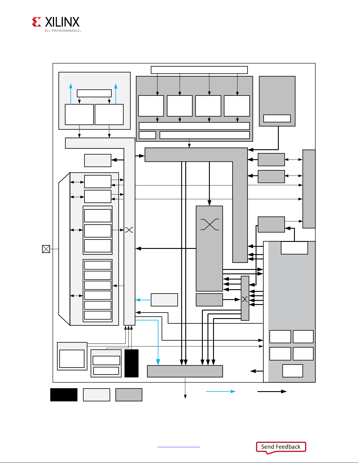
Block Diagram
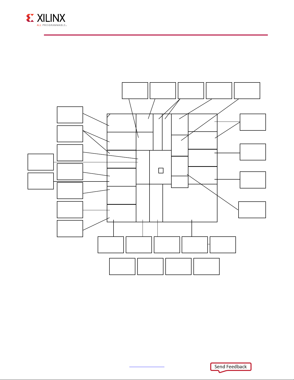
The ZCU102 board block diagram is shown in Figure 1-1. Page numbers in the block
diagram reference the corresponding page number(s) of schematic 0381701.
Figure 1-1: ZCU102 Evaluation Board Block Diagram
ZCU102 Evaluation Board User Guide www.xilinx.com 7
UG1182 (v1.2) March 20, 2017
Page 8

Chapter 1: Introduction
Send Feedback
Board Features
The ZCU102 evaluation board features are listed here. Detailed information for each feature
is provided in Chapter 3, Board Component Descriptions.
• XCZU9EG-2FFVB1156I MPSoC
•PL V
for range in datasheet
CCINT
• Form factor for PCIe Gen2x4 Host, Micro-ATX chassis footprint
• Configuration from QSPI
• Configuration from SD card
• Configuration over JTAG with PC4 header
• Configuration over JTAG with ARM 20-pin header
• Configuration over USB-to-JTAG Bridge
• Clocks (PL-system, PS_CLK, Programmable Clock, SMA, SMA_GT_REF, Ethernet, USB)
• PS DDR4 64-bit SODIMM w/ ECC
• PL DDR4 Component (16-bit)
• PS GTR assignment
SATA
°
DisplayPort
°
USB3
°
ZCU102 Evaluation Board User Guide www.xilinx.com 8
UG1182 (v1.2) March 20, 2017
PCIe Gen2x4 Root Port
°
• PL GTH assignment
FMC #1 (8 GTH) and FMC #2 (8 GTH) PL GT assignment
°
HDMI (3 GTH) PL GT assignment
°
SFP+ (4 GTH) PL GT assignment
°
SMA (1 GTH) PL GT assignment
°
• PL FMC HPC #1 Connectivity - Full LA Bus
• PL FMC HPC #2 Connectivity - Partial LA Bus
•PS MIO: QSPI
• PS MIO: Ethernet
• PS MIO: USB2 (same connector as USB3)
• PS MIO: SD
Page 9
•PS MIO: CAN
Send Feedback
• PS MIO: UART (using USB-to-UART bridge)
• PS MIO: Second UART
• PS MIO: I2C shared across PS and PL
•PS/PL EMIO: Trace
•PL-side UART
• PL-side LEDs (8)
• PL-side DIP switch (8-position)
• PL-side Pushbuttons (5)
• PS-side Pushbutton (1)
• PS-side LED (1)
• System User Switches (PROG, CPU Reset)
•PJTAG
Chapter 1: Introduction
• Security - PSBATT button battery backup
•SYSMON
• Operational Switches (Power on/off, PROG, Boot mode)
• Operational Status LEDs (power supply status, INIT, DONE, PG, JTAG status, DDR power
good)
• Power Management
The ZCU102 evaluation board provides designers a rapid prototyping platform utilizing the
XCZU9EG-2FFVB1156I device. The ZU9EG contains many useful processor system (PS) hard
block peripherals exposed through the Multi-use I/O (MIO) interface and a variety of FPGA
programmable logic (PL), high-density (HD) and high-performance (HP) banks. Table 1-1
lists a brief summary of the resources available within the ZU9EG. A feature set overview,
description, and ordering information is provided in the UltraScale Architecture and Product
Overview (DS890) [Ref 1].
Table 1-1: Zynq UltraScale+ MPSoC ZCU9EG Features and Resources
Feature Resource Count
HD banks 5 banks, total of 120 pins
HP banks 4 banks, total of 208 pins
ZCU102 Evaluation Board User Guide www.xilinx.com 9
UG1182 (v1.2) March 20, 2017
MIO banks 3 banks, total of 78 pins
PS-side GTR 6 Gb/s transceivers 4 PS-GTRs
PL-side GTH 16.3 Gb/s transceivers 24 GTHs
Effective LEs 575K
Page 10
Chapter 1: Introduction
Send Feedback
Table 1-1: Zynq UltraScale+ MPSoC ZCU9EG Features and Resources (Cont’d)
Feature Resource Count
Logic cells 480K
CLB flip-flops 548K
Max. distributed RAM 8.8 Mb
Total block RAM 32.1 Mb
DSP slices 2,520
Board Specifications
Dimensions
Width: 9.350 in. (23.749 cm)
Length: 9.600 in. (24.384 cm)
Thickness: 0.104 in. (0.2642 cm)
Notes:
• A 3D model of this board is not available.
• ZCU102 board documentation (xdc listing, schematics, layout files and board outline/fab
drawings, etc.) is available on the web at: www.xilinx.com/zcu102
.
Environmental
Temp erature
Operating: 0°C to +45°C
Storage: -25°C to +60°C
Humidity
10% to 90% non-condensing
Operating Voltage
ZCU102 Evaluation Board User Guide www.xilinx.com 10
UG1182 (v1.2) March 20, 2017
+12 V
DC
Page 11
Board Setup and Configuration
Send Feedback
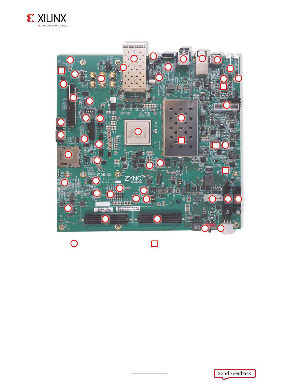
Board Component Location
Figure 2-1 shows the ZCU102 board component locations. Each numbered component
shown in Figure 2-1 is keyed to Table 2-1. Table 2-1 identifies the components, references
the respective schematic page numbers, and links to a detailed functional description of the
components and board features in Chapter 3.
IMPORTANT: Figure 2-1 is for visual reference only and might not reflect the latest revision of the
board. (This user guide documents ZCU102 Rev. 1.0 and later.)
IMPORTANT: There could be multiple revisions of this board. The specific details concerning the
differences between revisions is not captured in this document. This document is not intended to be a
reference design guide and the information herein should not be used as such. Always refer to the
schematic and xdc of the specific ZCU102 version of interest for such details.
Chapter 2
CAUTION! Electrostatic discharge (ESD) can cause board damage. Follow standard ESD prevention
measures when handling the board.
ZCU102 Evaluation Board User Guide www.xilinx.com 11
UG1182 (v1.2) March 20, 2017
Page 12
X-Ref Target - Figure 2-1
5RXQGFDOORXWUHIHUHQFHVDFRPSRQHQW
2QWKHIURQWVLGHRIWKHERDUG
6TXDUHFDOORXWUHIHUHQFHVDFRPSRQHQW
2QWKHEDFNVLGHRIWKHERDUG
;
Send Feedback
Chapter 2: Board Setup and Configuration
Figure 2-1: ZCU102 Evaluation Board Components
ZCU102 Evaluation Board User Guide www.xilinx.com 12
UG1182 (v1.2) March 20, 2017
Page 13
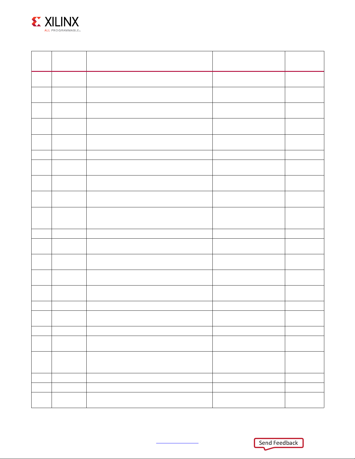
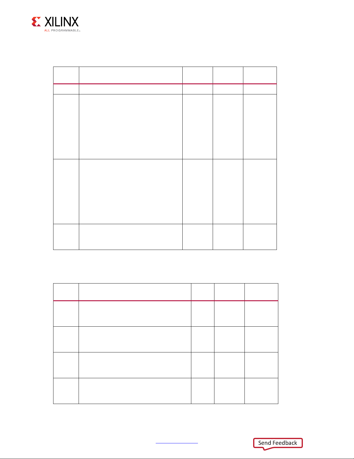
Table 2-1: ZCU102 Board Components
Send Feedback
Chapter 2: Board Setup and Configuration
Callout Ref. Des. Feature/Component Notes
Page Number
1
2
3
4
5
6J100SD Card Interface (connector) Hirose DMIAA-SF-PET(21) 47
7
8
9
10
11 U20 SFP/SFP+ Clock Recovery (jitter attenuated clock) Silicon Labs SI5328B-C-GMR 41
12
13
14
15
16 U34, U135 I2C1 (MIO 16-17) bus switches TI TCA9548APWR, 2ea. 58
17
18 U41 TI MSP430 System Controller TI MSP430F5342 38
19
20
21 DS37-DS44 User I/O (8 LEDs) GPIO LEDs, GREEN 0603 53
22 SW13
23
U1 Zynq UltraScale XCZU9EG MPSoC
with fan sink on soldered FPGA
J1 PS-Side: DDR4 SODIMM Socket
with SODIMM
U2 DDR4 Component Memory, (4 Gb) Micron
U119, U120 Quad-SPI Flash Memory (MIO 0–12) (1 Gb total) Micron
U116, J96 USB 3.0 Transceiver and USB 2.0 ULPI PHY (USB
micro-AB connector)
U21/J2 Programmable Logic JTAG Programming Options
(module with separate USB Micro-B conn.)
U42 Programmable User Clock
(300 MHz default, 3.3V LVDS)
U56 Programmable User MGT Clock
(156.250 MHz default, 3.3V LVDS)
U69 SI5341B 10 Independent Output Any-Frequency
Clock Generator (PS Reference Clock) (I2C
programmable any frequency clock generator)
U98/P12 Ethernet PHY LED Interface Ethernet PHY U98 with
P12 RJ45 with magnetics
U40/J83 CP2108 USB UART Interface (bridge IC/USB Micro-B
connector)
U94/P7 HDMI Video Output (controller/connector) TI SN65DP159RGZ,
U60, U61,
U97
J54 SFP/SFP+ Connector (quad) Allbest
J55/J87 User PMOD GPIO Headers
J160 For more information about PMOD connector
SW14-SW18 User I/O (pushbutton switches, active High) E-Switch TL3301EP100QG
I2C0 (MIO 14-15) bus switch and expanders) TI PCA9544ARGYR, 2 ea.
(PMOD0-RA receptacle/PMOD1-vert. male pin hdr.)
compatible PMOD modules, see [Ref 23]. (PMOD I2C
RA receptacle)
User I/O (8-pole DIP switch) C&K SDA08H1SBD 53
XCZU9EG-2FFVB1156I
Radian FA35+K52B+T710
LOTES ADDR0067-P001A
Micron
MT40A256M16GE-075E:B
MT25QU512ABB8ESF-OSIT
SMCS USB3320-EZK, KYON
KMMX-AB10-SMT1SB30TR
Digilent JTAG_2_NC,
Hirose ZX62D-AB-5P8
Silicon Labs
SI570BAB001614DG
Silicon Labs SI
SI570BAB001544DG
Silicon Labs
SI5341B-B05071-GM 39
TI DP83867IRPAP,
Wurth 7499111221A
Silicon Labs CP2108-B02-GM,
Hirose ZX62D-AB-5P8
TEC Connectivity 1888811-1
TI TCA6416APWR
R-OP-008080-6-F-N-26-F63
SULLINS PPPO062LJBN-RC,
SULLINS PBC36DAAN
SULLINS PPPO062LJBN-RC
placed in N, S, W, E, C pattern
Schematic
0381449
23
25
46
51
22
40
40
52
42
35
57
34
55
49
53
ZCU102 Evaluation Board User Guide www.xilinx.com 13
UG1182 (v1.2) March 20, 2017
Page 14

Table 2-1: ZCU102 Board Components (Cont’d)
Send Feedback
Chapter 2: Board Setup and Configuration
Callout Ref. Des. Feature/Component Notes
0381449
Page Number
24 SW20 User I/O (CPU_RESET pushbutton switch, active High) E-Switch TL3301EP100QG 53
Schematic
25
26
27
28
29 J52 Power connector (Power On/Off Slide Switch) MOLEX 39-30-1060 59
30 SW5 Program_B Pushbutton (FPGA program) E-Switch TL3301EP100QG 12
31 J5 FMC HPC0 Connector J5 Samtec ASP_134486_01 26-29
32 J4 FMC HPC1 Connector J4 Samtec ASP_134486_01 30-33
33 J10 Switched output power connector TEC Connectivity 794285-1 59
34 - Power management system (top and bottom) Maxim Regulators 59-86
35 P1 PCI Express Root Port Slot (PCIe 4-lane connector) FCI 10061913-101CLF 43
36 P11 DPAUX (MIO 27-30) (DisplayPort) MOLEX 0472720001 44
37 J84 PMBus connector (Monitoring Voltage and Current) ASSMANN
38 J92 JTAG connector (TI MSP430 System Controller) TYCO 5103308-2 38
39 J6 ARM JTAG connector (Programmable Logic JTAG
40 U108 HDMI Clock Recovery (HDMI jitter attenuated clock) Silicon Labs SI 5324C-C-GMR 37
41 J3 For more information about PMOD connector
42 J70-J72
43 P6 EMIO ARM Trace Port (ARM Trace receptacle) MICTOR 2-5767004-2 54
44 SW6 Switches (mode 4-pole DIP switch) 4-pole C&K SDA04H1SBD 12
45 (Misc. DSnn) Power and Status LEDs (Misc. LEDs) Miscellaneous LEDs 86
SW8 DIP Switch, 5-pole, GPIO (TI MSP430 System
Controller)
SW3, SW4 Switches (SRST_RESET, POR_B pushbutton switches,
active Low)
U122, J98 CAN1 (MIO 24-25) (bus transceiver/2x4 male header) TI SN65HVD232,
SW1 Power On/Off Slide Switch (Power On/Off slide
switch)
Programming Options)
compatible PMOD modules, see [Ref 23]. MPSoC U1
Bank 50 GPIO 2x12 male pin proto header
SMA (MGTH interface SMA connectors) ROSENBERGER
J79-J80
5 pole C&K SDA05H1SBD 38
E-Switch TL3301EP100QG 12
SULLINS PBC36DAAN
C&K 1201M2S3AQE2 59
AWHW16G-0202-T-R
ASSMANN
AWHW20G-0202-T-R
SULLINS PBC36DAAN
32K10K-400L5
50
57
22
56
40
ZCU102 Evaluation Board User Guide www.xilinx.com 14
UG1182 (v1.2) March 20, 2017
Page 15
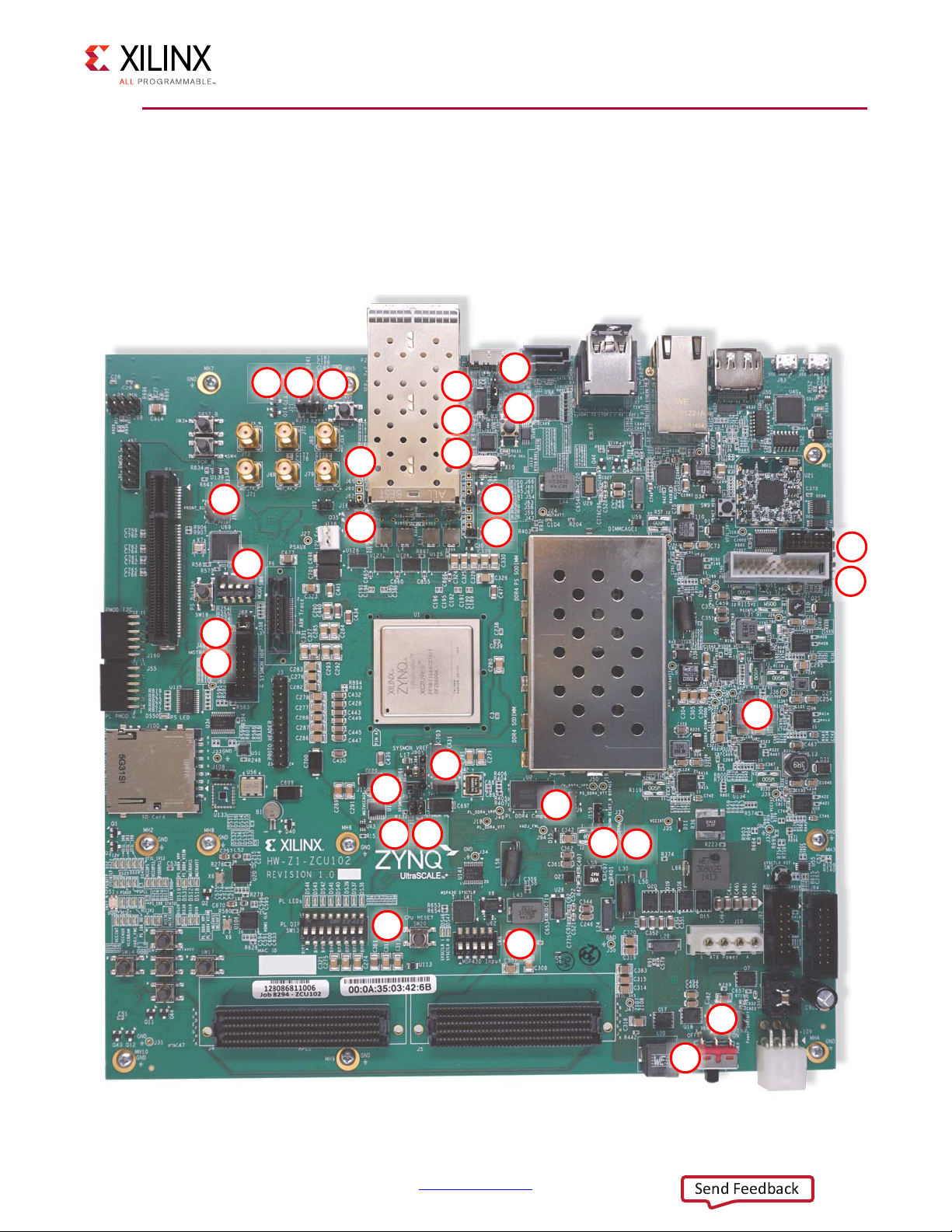
X-Ref Target - Figure 2-2
;
Send Feedback
Chapter 2: Board Setup and Configuration
Default Switch and Jumper Settings
Figure 2-2 shows the board jumper header and DIP switch locations. Each numbered
component shown in the figure is keyed to Table 2-2 (for default switch settings) or
Table 2-3 (for default jumper settings). Both tables reference the respective schematic page
numbers.
ZCU102 Evaluation Board User Guide www.xilinx.com 15
UG1182 (v1.2) March 20, 2017
Figure 2-2: DIP Switch and Board Header Jumper Locations
Page 16
Switches
Send Feedback
Table 2-2: Default Switch Settings
Chapter 2: Board Setup and Configuration
DIP
Switch
SW1 Main Power Switch OFF 29 59
Switch PS_MODE select
• ON = pull down =
• OFF = pull up = 1
SW6
SW8
SW13
• MODE[3:0] = 0010 (selects QSPI32)
MSP430 GPIO 5-POLE
•ON = GND
• OFF = Open
GPIO 8-POLE
• OFF = pull down
• ON = pull up
Function Default
0
4: PS_MODE3
3: PS_MODE2
2: PS_MODE1
1: PS_MODE0
1: SW0
2: SW1
3: SW2
4: SW3
5: SW4
ON
ON
OFF
ON
OFF
OFF
OFF
OFF
OFF
All OFF 28 53
Figure 2-2
Callout
26 12
27 38
Schematic
Page
Jumpers
Table 2-3: Default Jumper Settings
Jumper Function Default
POR_OVERRIDE
J85
J12
J13
J90
• 1-2: Enable
•2-3: Disable
SYSMON I2C Address
• Open: SYSMON_VP_R floating
• 1-2: SYSMON_VP_P pulled down
SYSMON I2C Address
• Open: SYSMON_VN_R floating
• 1-2: SYSMON_VP_N pulled down
SYSMON VREFP
• 1-2: 1.25V VREFP connected to FPGA
• 2-3: VREFP connected to GND
2-3 1 3
1-2 2 3
1-2 3 3
1-2 4 3
Figure 2-2
Callout
Schematic
Page
ZCU102 Evaluation Board User Guide www.xilinx.com 16
UG1182 (v1.2) March 20, 2017
Page 17
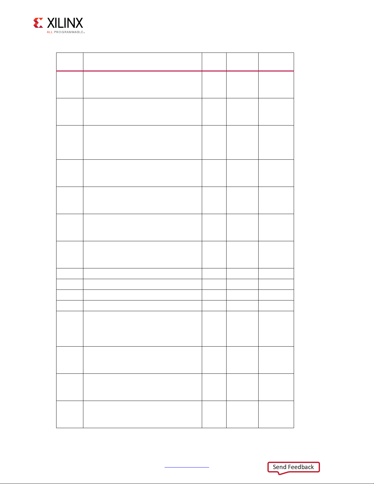
Table 2-3: Default Jumper Settings (Cont’d)
Send Feedback
Chapter 2: Board Setup and Configuration
Jumper Function Default
Reset Sequencer PS_POR_B
J20
J21
J22
J14
J15
J56
• OFF: No sequencer control of PS_POR_B
• 1-2: Sequencer can control PS_POR_B
Reset Sequencer PS_SRST_B
• OFF: No sequence control of PS_SRST_B
• 1-2: Sequencer can control PS_SRST_B
Reset Sequencer inhibit
• OFF: Sequencer normal operation
• 1-2: Sequencer inhibit (resets will stay
asserted)
ARM Debug VTREF
•Open: VTREF floating
• 1-2: VTREF = VCCOPS3 (1.8V)
ARM Debug VSUPPLY
• OFF: VSUPPLY floating
• 1-2: VSUPPLY = VCCOPS3 (1.8V)
VCCO_PSDDR_504 select
• 1-2: Switched DDR4 VDDQ
• 3-4: Direct DDR4 VDDQ
1-2 5 12
1-2 6 12
OFF 7 12
1-2 8 22
OFF 9 22
1-2 10 24
Figure 2-2
Callout
Schematic
Page
DDR4 Reset Suspend Enable
J159
J16 SFP0 TX: 1-2:Disable; OFF: Enable OFF 12 34
J17 SFP1 TX: 1-2:Disable; OFF: Enable OFF 12 34
J42 SFP2 TX: 1-2:Disable; OFF: Enable OFF 14 34
J54 SFP3 TX: 1-2:Disable; OFF: Enable OFF 15 34
J162
J110
J109
J112
• 1-2: Suspend disabled (Gate bypass)
• 2-3: Suspend enabled
PCIe PRSNT select
•1-2: x1
•3-4: x4
•5-6: GND (not used)
USB ULPI CVBUS Select
•1-2: DEVICE or OTG Mode
• 2-3: Host Mode
USB ULPI ID select
• 1-2: Connector ID
• 2-3: VDD33 ID
USB ULPI Shield GND select
•1-2: Capacitor
•2-3: GND
1-2 11 24
5-6 16 43
1-2 17 51
2-3 18 51
1-2 19 51
ZCU102 Evaluation Board User Guide www.xilinx.com 17
UG1182 (v1.2) March 20, 2017
Page 18
Table 2-3: Default Jumper Settings (Cont’d)
Send Feedback
Chapter 2: Board Setup and Configuration
Jumper Function Default
USB ULPI Device or Host select
J7
J113
J88
J38
J153
J9
• 1-2: HOST/OTG
•Open: Device
USB ULPI Device/Host or OTG select
• 1-2: Device or Host
•2-3: OTG
ARM Trace VTREF
• 1-2: 3.3V
•Open: 0V
ARM Trace power
• 1-2: 3.3V
•Open: 0V
Power inhibit
• OFF: rails power on normally
• 1-2: all rails (except UTIL) OFF
PS_DDR4_VPP_2V5 power inhibit (U39)
• OFF: rail powers on normally
• 1-2: PS_DDR4_VPP_2V5 OFF
OPEN 20 51
1-2 21 51
1-2 22 54
1-2 23 54
OFF 24 59
OFF 25 77
Figure 2-2
Callout
Schematic
Page
J164 MSP430 firmware upgrade header OFF 26 38
ZCU102 Evaluation Board User Guide www.xilinx.com 18
UG1182 (v1.2) March 20, 2017
Page 19
Chapter 2: Board Setup and Configuration
Send Feedback
MPSoC Device Configuration
Zynq UltraScale+ XCZU9EG MPSoC devices use a multi-stage boot process documented in
the Boot and Configuration chapter of the Zynq UltraScale+ MPSoC Technical Reference
Manual (UG1085) [Ref 2].
Switch SW6 configuration option settings are identified in Table 2-4.
Table 2-4: Switch SW6 Configuration Option Settings
Boot Mode Mode Pins [3:0] Mode SW6 [4:1]
JTAG
QSPI32
SD
Notes:
1. Default switch setting.
0000
0010
1110
(1)
on, on, on, on
on, on, off, on
off, off, off, on
JTAG
Vivado, SDK, or third-party tools can establish a JTAG connection to the Zynq UltraScale+
MPSoC device through one of the three provided JTAG interfaces:
1. Xilinx platform USB or cable PC4 connector (J8)
2. ARM 20-pin JTAG connector (J6)
3. Digilent SMT2.5 USB-to-JTAG module with off-module micro-USB connector (J2)
Quad-SPI
Booting from the dual Quad-SPI nonvolatile configuration memory is accomplished by
storing a valid Zynq UltraScale+ MPSoC boot image into the Quad-SPI flash devices
connected to the MIO Quad-SPI interface, setting the boot mode pins SW6 [4:1] = QSPI32
(see Table 2-4), then either power-cycling or pressing the power-on reset (POR) pushbutton.
SW6 is callout 23 in Figure 2-1.
ZCU102 Evaluation Board User Guide www.xilinx.com 19
UG1182 (v1.2) March 20, 2017
SD
Booting from an SD card is accomplished by storing a valid Zynq UltraScale+ MPSoC boot
image file onto an SD card (plugged into SD socket J100) connected to the MIO SD
interface, setting the boot mode pins SW6 [4:1] = SD (see Table 2-4), then either
power-cycling or pressing the power-on reset (POR) pushbutton.
See the Zynq UltraScale+ MPSoC Technical Reference Manual (UG1085) [Ref 2] for more
information about Zynq UltraScale+ MPSoC configuration options.
Page 20
Board Component Descriptions
Send Feedback
Overview
This chapter provides a detailed functional description of the board’s components and
features. Table 2-1, page 13 identifies the components, references the respective schematic
page numbers, and links to the corresponding detailed functional description in this
chapter. Component locations are shown in Figure 2-1, page 12.
Component Descriptions
Chapter 3
Zynq UltraScale XCZU9EG MPSoC
[Figure 2-1, callout 1]
The ZCU102 board is populated with the Zynq UltraScale+ XCZU9EG-2FFVB1156I MPSoC
which combines a powerful processing system (PS) and user-programmable logic (PL) into
the same device. The processing system in a Zynq UltraScale+ MPSoC features the ARM®
flagship Cortex®-A53 64-bit quad-core processor and Cortex-R5 dual-core real-time
processor.
Production ZCU102 Evaluation boards will ship with -2LE speed grade devices. Support of
multiple speed grades requires voltage adjustments.
The PL-side V
in Table 3-1 to support multiple Zynq UltraScale+ MPSoC speed grades.
Table 3-1: Recommended Operating Conditions
Symbol Description Min. Typ. Max Units
Programmable Logic (PL)
V
CCINT
supply will be user adjustable via PMBUS with the voltage ranges shown
CCINT
Internal supply voltage.
For -1LI and -2LE devices: internal supply voltage.
For -3E devices: internal supply voltage.
0.825 0.850 0.875 V
0.698 0.720 0.742 V
0.873 0.900 0.927 V
ZCU102 Evaluation Board User Guide www.xilinx.com 20
UG1182 (v1.2) March 20, 2017
Page 21
X-Ref Target - Figure 3-1
RPU
256 KB
OCM
LPD-DMA
CSU
PMU
Processing System
Cortex-R5
32 KB I/D
128 KB TCM
Cortex-R5
32 KB I/D
128 KB TCM
4 x 1GE
APU
Cortex-A53
32 KB I/D
Cortex-A53
32 KB I/D
Cortex-A53
32 KB I/D
Cortex-A53
32 KB I/D
GIC
SCU
ACP 1 MB L2
GPU
Mali-400 MP2
64 KB L2
2 x USB 3.0
NAND x8
ONFI 3.1
2 x SD3.0/
eMMC4.51
Quad-SPI
x 8
2 x SPI
2 x CAN
2 x I2C
2 x UART
GPIOs
SYSMON
MIO
Central
Switch
FPD-DMA
PCIe
Gen4
DisplayPort
v1.2 x1, x2
2 x SATA
v3.1
PCIe Gen2
x1, x2, or x4
SHA3
AES-GCM
RSA
Processor
System
BPU
DDRC (DDR4/3/3L, LPDDR3/4)
Programmable
Logic
128 KB RAM
PL_LPD
HP
GIC
RGMII
ULPI
PS-GTR
SMMU/CCI
GFC
USB 3.0
SGMII
Low Power Switch
To ACP
Low Power Full Power
Battery
Power
32-bit/64-bit
64-bit
MS
128-bit
MS
LPD_PL HPCHPM
GTY
Quad
GTH
Quad
Interlaken
100G
Ethernet
ACE
DisplayPort
Video and
Audio Interface
Low-latency
Peripheral Port
Low-latency
Peripheral Port
;
Send Feedback
Chapter 3: Board Component Descriptions
The top-level block diagram is shown in Figure 3-1.
ZCU102 Evaluation Board User Guide www.xilinx.com 21
UG1182 (v1.2) March 20, 2017
Figure 3-1: Zynq UltraScale+ MPSoC Top-Level Block Diagram
Page 22

Chapter 3: Board Component Descriptions
Send Feedback
The Zynq UltraScale+ MPSoC PS block has three major processing units:
Cortex-A53 application processing unit (APU)-ARM v8 architecture-based 64-bit
°
quad-core multiprocessing CPU.
Cortex-R5 real-time processing unit (RPU)-ARM v7 architecture-based 32-bit dual
°
real-time processing unit with dedicated tightly coupled memory (TCM).
Mali-400 graphics processing unit (GPU)-graphics processing unit with pixel and
°
geometry processor and 64 KB L2 cache.
The Zynq UltraScale+ MPSoC PS has four high-speed serial I/O (HSSIO) interfaces
supporting the following protocols:
Integrated block for PCI Express® interface-PCIe™ base specification version 2.1
°
compliant.
SATA 3.1 specification compliant interface.
°
DisplayPort interface-implements a DisplayPort source-only interface with video
°
resolution up to 4K x 2K-30 (300 MHz pixel rate).
USB 3.0 interface-compliant to USB 3.0 specification implementing a 5 Gb/s line
°
rate.
Serial GMII interface-supports a 1 Gb/s SGMII interface.
°
The PS and PL can be coupled with multiple interfaces and other signals to effectively
integrate user-created hardware accelerators and other functions in the PL logic that are
accessible to the processors. They can also access memory resources in the processing
system. The PS I/O peripherals, including the static/flash memory interfaces share a
multiplexed I/O (MIO) of up to 78 MIO pins. Zynq UltraScale+ MPSoCs can also use the I/O
in the PL domain for many of the PS I/O peripherals. This is done through an extended
multiplexed I/O interface (EMIO).and boots at power-up or reset.
For additional information on Zynq UltraScale+ MPSoC devices, see the UltraScale
Architecture and Product Overview (DS890) [Ref 1], and the Zynq UltraScale+ MPSoC
Technical Reference Manual (UG1085) [Ref 2] for more information about Zynq UltraScale+
MPSoC configuration options.
ZCU102 Evaluation Board User Guide www.xilinx.com 22
UG1182 (v1.2) March 20, 2017
Page 23
Chapter 3: Board Component Descriptions
;
Send Feedback
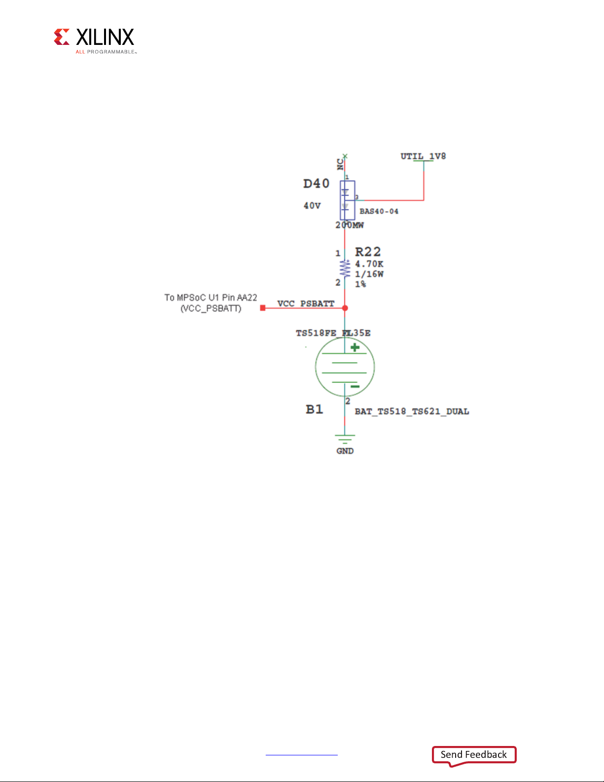
Encryption Key Backup Circuit
The XCZU9EG MPSoC U1 implements bitstream encryption key technology. The ZCU102
board provides the encryption key backup battery circuit shown in Figure 3-2
X-Ref Target - Figure 3-2
ZCU102 Evaluation Board User Guide www.xilinx.com 23
UG1182 (v1.2) March 20, 2017
Figure 3-2: Encryption Key Backup Circuit
The Seiko TS518FE rechargeable 1.5V lithium button-type battery B1 is soldered to the
board with the positive output connected to the XCZU9EG MPSoC U1 V
The battery supply current I
specification is 150 nA maximum when board power is off.
BATT
CC_PSBATT
pin AA22.
B1 is charged from the UTIL_1V8 1.8V rail through a series diode with a typical forward
voltage drop of 0.38V and 4.7 ΩK current limit resistor. The nominal charging voltage is
1.42V.
Page 24

Chapter 3: Board Component Descriptions
Send Feedback
I/O Voltage Rails
There are nine PL I/O banks available on the XCZU9EG MPSoC. The voltages applied to the
XCZU9EG MPSoC I/O banks used by the ZCU102 board are listed in Table 3-2.
Table 3-2: I/O Voltage Rails
XCZU9EG Power Net Name Voltage Connected To
PL Bank 0
PL Bank 44
PL Bank 47
PL Bank 48
PL Bank 49
PL Bank 50
PL Bank 64
PL Bank 65
PL Bank 66
PL Bank 67
PS Bank 500
PS Bank 501
PS Bank 502
PS Bank 503
PS DDR Bank 504
NA NA
V
CC3V3
V
CC3V3
V
CC3V3
V
CC3V3
V
CC3V3
V
CC1V2
V
CCOPS
V
CCOPS
V
CCOPS
CCOPS3
(1)
(1)
(1)
V
ADJ_FMC
V
ADJ_FMC
V
ADJ_FMC
V
V
CCO_PSDDR_504
3.3V
3.3V
3.3V
3.3V
3.3V
1.2V
1.8V
1.8V
1.8V
1.8V
1.8V
1.8V
1.81V
1.2V
MPSoC Configuration Bank 0
GPIO DIP SW, PB SW, LEDs, 74.25 MHz CLK
GPIO PMOD0 (RT-ANG. FEMALE), PMOD1 (STR.
MALE), PL I2C1, TRACEDATA, 125 MHz CLK
TRACEDATA
HDMI Codec, SYSMON I2C, SFP CTRL, UART2, MSP430
UCA1
HDMI Codec, MSP430 GPIO, PL I2C0, PROTO. HDR. IO
DDR4 DQ[0:15], DDR4 ADDR/CTRL, USER_SI570 CLK
FMC_HPC1 LA BUS, HDMI TX
FMC_HPC0 LA BUS, HDMI REC CLK
FMC_HPC0 LA BUS, SFP REC CLK
QSPI LWR, QSPI UPR, UART1, MIO_I2C0, MIO_I2C1,
MIO_RXD/TXD, CAN IF
MIO_SD IF, MIO_PMU IF, MIO_DP IF
MIO_ENET, MIO_USB
PS CONFIGURATION IF
DDR4 SODIMM IF
ZCU102 Evaluation Board User Guide www.xilinx.com 24
UG1182 (v1.2) March 20, 2017
Notes:
1. The ZCU102 board is shipped with V
ADJ_FMC
set to 1.8V by the MSP430 system controller.
PS-Side: DDR4 SODIMM Socket
[Figure 2-1, callout 2]
The PS-side memory is wired to the Zynq UltraScale+ DDRC hard memory controller. A
64-bit single rank DDR4 SODIMM with ECC (72-bit) is inserted into socket J1. The ZCU102
is shipped with a DDR4 SODIMM installed:
• Manufacturer: Kingston
• Part Number: KVR21SE15S8/4
•Description:
4GByte DDR4 SODIMM
°
Single Rank x8
°
512Mbit x 72-Bit
°
PC4-2133 260-Pin
°
Page 25
Chapter 3: Board Component Descriptions
Send Feedback
The ZCU102 supports full power-off suspend mode where only the system controller and
the PS-side DDR4 SODIMM memory are powered. The DDR4 memory is kept in a
self-refresh state and has its reset input controlled by the system controller such that the
memory is not reset when waking-up from suspend mode. DDR4 SODIMM standard right
angle Socket J1 connections are identified in Table 3-3.
Table 3-3: DDR4 SODIMM Socket J1 Connections to FPGA PS DDR Bank 504
XCZU9EG
(U1) Pin
AP29
AP30
AP26
AP27
AP25
AN24
AM29
AM28
AM26
AM25
AL28
AK27
AJ25
AL25
AH26
Net Name
DDR4 SODIMM Memory J1
Pin Number Pin Name
DDR4_SODIMM_A0 144 A0
DDR4_SODIMM_A1 133 A1
DDR4_SODIMM_A2 132 A2
DDR4_SODIMM_A3 131 A3
DDR4_SODIMM_A4 128 A4
DDR4_SODIMM_A5 126 A5
DDR4_SODIMM_A6 127 A6
DDR4_SODIMM_A7 122 A7
DDR4_SODIMM_A8 125 A8
DDR4_SODIMM_A9 121 A9
DDR4_SODIMM_A10 146 A10/AP
DDR4_SODIMM_A11 120 A11
DDR4_SODIMM_A12 119 A12
DDR4_SODIMM_A13 158 A13
DDR4_SODIMM_BA0 150 BA0
ZCU102 Evaluation Board User Guide www.xilinx.com 25
UG1182 (v1.2) March 20, 2017
AG26
AK28
AH27
AP20
AP18
AP19
AP17
AM20
AM19
AM18
AL18
AP22
AP21
AP24
DDR4_SODIMM_BA1 145 BA1
DDR4_SODIMM_BG0 115 BG0
DDR4_SODIMM_BG1 113 BG1
DDR4_SODIMM_DQ0 8 DQ0
DDR4_SODIMM_DQ1 7 DQ1
DDR4_SODIMM_DQ2 20 DQ2
DDR4_SODIMM_DQ3 21 DQ3
DDR4_SODIMM_DQ4 4 DQ4
DDR4_SODIMM_DQ5 3 DQ5
DDR4_SODIMM_DQ6 16 DQ6
DDR4_SODIMM_DQ7 17 DQ7
DDR4_SODIMM_DQ8 28 DQ8
DDR4_SODIMM_DQ9 29 DQ9
DDR4_SODIMM_DQ10 41 DQ10
Page 26
Chapter 3: Board Component Descriptions
Send Feedback
Table 3-3: DDR4 SODIMM Socket J1 Connections to FPGA PS DDR Bank 504 (Cont’d)
XCZU9EG
(U1) Pin
AN23
AL21
AL22
AM23
AL23
AL20
AK20
AJ20
AK18
AG20
AH18
AG19
AG18
AG21
AH21
Net Name
DDR4 SODIMM Memory J1
Pin Number Pin Name
DDR4_SODIMM_DQ11 42 DQ11
DDR4_SODIMM_DQ12 24 DQ12
DDR4_SODIMM_DQ13 25 DQ13
DDR4_SODIMM_DQ14 38 DQ14
DDR4_SODIMM_DQ15 37 DQ15
DDR4_SODIMM_DQ16 50 DQ16
DDR4_SODIMM_DQ17 49 DQ17
DDR4_SODIMM_DQ18 62 DQ18
DDR4_SODIMM_DQ19 63 DQ19
DDR4_SODIMM_DQ20 46 DQ20
DDR4_SODIMM_DQ21 45 DQ21
DDR4_SODIMM_DQ22 58 DQ22
DDR4_SODIMM_DQ23 59 DQ23
DDR4_SODIMM_DQ24 70 DQ24
DDR4_SODIMM_DQ25 71 DQ25
AG24
AG23
AK22
AJ21
AJ22
AK23
AG31
AG30
AG29
AG28
AJ30
AK29
AK30
AJ29
AE27
AF28
AF30
DDR4_SODIMM_DQ26 83 DQ26
DDR4_SODIMM_DQ27 84 DQ27
DDR4_SODIMM_DQ28 66 DQ28
DDR4_SODIMM_DQ29 67 DQ29
DDR4_SODIMM_DQ30 79 DQ30
DDR4_SODIMM_DQ31 80 DQ31
DDR4_SODIMM_DQ32 174 DQ32
DDR4_SODIMM_DQ33 173 DQ33
DDR4_SODIMM_DQ34 187 DQ34
DDR4_SODIMM_DQ35 186 DQ35
DDR4_SODIMM_DQ36 170 DQ36
DDR4_SODIMM_DQ37 169 DQ37
DDR4_SODIMM_DQ38 183 DQ38
DDR4_SODIMM_DQ39 182 DQ39
DDR4_SODIMM_DQ40 195 DQ40
DDR4_SODIMM_DQ41 194 DQ41
DDR4_SODIMM_DQ42 207 DQ42
ZCU102 Evaluation Board User Guide www.xilinx.com 26
UG1182 (v1.2) March 20, 2017
AF31
AD28
DDR4_SODIMM_DQ43 208 DQ43
DDR4_SODIMM_DQ44 191 DQ44
Page 27

Chapter 3: Board Component Descriptions
Send Feedback
Table 3-3: DDR4 SODIMM Socket J1 Connections to FPGA PS DDR Bank 504 (Cont’d)
XCZU9EG
(U1) Pin
AD27
AD29
AD30
AH33
AJ34
AH34
AH32
AK34
AK33
AL32
AL31
AG33
AG34
AF32
AF33
Net Name
DDR4 SODIMM Memory J1
Pin Number Pin Name
DDR4_SODIMM_DQ45 190 DQ45
DDR4_SODIMM_DQ46 203 DQ46
DDR4_SODIMM_DQ47 204 DQ47
DDR4_SODIMM_DQ48 216 DQ48
DDR4_SODIMM_DQ49 215 DQ49
DDR4_SODIMM_DQ50 228 DQ50
DDR4_SODIMM_DQ51 229 DQ51
DDR4_SODIMM_DQ52 211 DQ52
DDR4_SODIMM_DQ53 212 DQ53
DDR4_SODIMM_DQ54 224 DQ54
DDR4_SODIMM_DQ55 225 DQ55
DDR4_SODIMM_DQ56 237 DQ56
DDR4_SODIMM_DQ57 236 DQ57
DDR4_SODIMM_DQ58 249 DQ58
DDR4_SODIMM_DQ59 250 DQ59
AD31
AD32
AD34
AD33
AN31
AP31
AP32
AP33
AM31
AM33
AM34
AL33
AN17
AM21
AK19
AH24
AH31
DDR4_SODIMM_DQ60 232 DQ60
DDR4_SODIMM_DQ61 233 DQ61
DDR4_SODIMM_DQ62 245 DQ62
DDR4_SODIMM_DQ63 246 DQ63
DDR4_SODIMM_CB0 92 CB0/NC
DDR4_SODIMM_CB1 91 CB1/NC
DDR4_SODIMM_CB2 101 CB2/NC
DDR4_SODIMM_CB3 105 CB3/NC
DDR4_SODIMM_CB4 88 CB4/NC
DDR4_SODIMM_CB5 87 CB5/NC
DDR4_SODIMM_CB6 100 CB6/NC
DDR4_SODIMM_CB7 104 CB7/NC
DDR4_SODIMM_DM0_B 12 DM0_N/DBI0_N
DDR4_SODIMM_DM1_B 33 DM1_N/DBI1_N
DDR4_SODIMM_DM2_B 54 DM2_N/DBI2_N
DDR4_SODIMM_DM3_B 75 DM3_N/DBI3_N
DDR4_SODIMM_DM4_B 178 DM4_N/DBI4_N
ZCU102 Evaluation Board User Guide www.xilinx.com 27
UG1182 (v1.2) March 20, 2017
AE30
AJ31
DDR4_SODIMM_DM5_B 199 DM5_N/DBI5_N
DDR4_SODIMM_DM6_B 220 DM6_N/DBI6_N
Page 28

Chapter 3: Board Component Descriptions
Send Feedback
Table 3-3: DDR4 SODIMM Socket J1 Connections to FPGA PS DDR Bank 504 (Cont’d)
XCZU9EG
(U1) Pin
AE34
AN34
AN18
AN19
AN21
AN22
AH19
AJ19
AH22
AH23
AH28
AH29
AE28
AE29
AJ32
Net Name
DDR4 SODIMM Memory J1
Pin Number Pin Name
DDR4_SODIMM_DM7_B 241 DM7_N/DBI7_N
DDR4_SODIMM_DM8_B 96 DM8_N/DBI8_N/NC
DDR4_SODIMM_DQS0_T 13 DQS0_T
DDR4_SODIMM_DQS0_C 11 DQS0_C
DDR4_SODIMM_DQS1_T 34 DQS1_T
DDR4_SODIMM_DQS1_C 32 DQS1_C
DDR4_SODIMM_DQS2_T 55 DQS2_T
DDR4_SODIMM_DQS2_C 53 DQS2_C
DDR4_SODIMM_DQS3_T 76 DQS3_T
DDR4_SODIMM_DQS3_C 74 DQS3_C
DDR4_SODIMM_DQS4_T 179 DQS4_T
DDR4_SODIMM_DQS4_C 177 DQS4_C
DDR4_SODIMM_DQS5_T 200 DQS5_T
DDR4_SODIMM_DQS5_C 198 DQS5_C
DDR4_SODIMM_DQS6_T 221 DQS6_T
AK32
AE32
AE33
AN32
AN33
AN27
AN26
AL27
AL26
AN29
AJ27
AM30
AJ26
AM24
AK24
AK25
AG25
DDR4_SODIMM_DQS6_C 219 DQS6_C
DDR4_SODIMM_DQS7_T 242 DQS7_T
DDR4_SODIMM_DQS7_C 240 DQS7_C
DDR4_SODIMM_DQS8_T 97 DQS8_T
DDR4_SODIMM_DQS8_C 95 DQS8_C
DDR4_SODIMM_CK0_C 139 CK0_C
DDR4_SODIMM_CK0_T 137 CK0_T
DDR4_SODIMM_CK1_C 140 CK1_C/NF
DDR4_SODIMM_CK1_T 138 CK1_T/NF
DDR4_SODIMM_CKE0 109 CKE0
DDR4_SODIMM_CKE1 110 CKE1
DDR4_SODIMM_ODT0 155 ODT0
DDR4_SODIMM_ODT1 161 ODT1
DDR4_SODIMM_RAS_B 152 RAS_N/A16
DDR4_SODIMM_CAS_B 156 CAS_N/A15
DDR4_SODIMM_WE_B 151 WE_N/A14
DDR4_SODIMM_ACT_B 114 ACT_N
ZCU102 Evaluation Board User Guide www.xilinx.com 28
UG1182 (v1.2) March 20, 2017
AF22
AF20
DDR4_SODIMM_ALERT_B 116 ALERT_N
DDR4_SODIMM_PARITY 143 PARITY
Page 29

Chapter 3: Board Component Descriptions
Send Feedback
Table 3-3: DDR4 SODIMM Socket J1 Connections to FPGA PS DDR Bank 504 (Cont’d)
XCZU9EG
(U1) Pin
AN28
AL30
Net Name
DDR4_SODIMM_CS0_B 149 CS0_N
DDR4_SODIMM_CS1_B 157 CS1_N
DDR4 SODIMM Memory J1
Pin Number Pin Name
The ZCU102 DDR4 SODIMM interface adheres to the constraints guidelines documented in
the PCB Guidelines for DDR4 section of UltraScale Architecture PCB Design Guide (UG583)
[Ref 3] The ZCU102 DDR4 SODIMM interface is a 40Ω impedance implementation. Other
memory interface details are also available in the UltraScale Architecture FPGAs Memory
Interface Solutions Guide (PG150) [Ref 4].
DDR4 Component Memory
[Figure 2-1, callout 3]
The 4 Gb, 16-bit wide DDR4 memory system is comprised of one 256 Mb x 16 SDRAM
(Micron MT40A256M16GE-075E) at U2. This memory system is connected to the PL-side
XCZU9EG bank 64. The DDR4 0.6V VTT termination voltage is supplied from sink-source
regulator U35. The connections between the DDR4 memory and XCZU9EG bank 64 are
listed in Table 3-4.
Table 3-4: DDR4 Component Memory Connection to the XCZU9EG MPSoC
XCZU9EG
(U1) Pin
AM8
AM9
AP8
AN8
AK10
AJ10
AP9
AN9
AP10
AP11
AM10
AL10
AM11
AL11
Net Name I/O Standard
DDR4_A0 SSTL12_DCI P3 A0
DDR4_A1 SSTL12_DCI P7 A1
DDR4_A2 SSTL12_DCI R3 A2
DDR4_A3 SSTL12_DCI N7 A3
DDR4_A4 SSTL12_DCI N3 A4
DDR4_A5 SSTL12_DCI P8 A5
DDR4_A6 SSTL12_DCI P2 A6
DDR4_A7 SSTL12_DCI R8 A7
DDR4_A8 SSTL12_DCI R2 A8
DDR4_A9 SSTL12_DCI R7 A9
DDR4_A10 SSTL12_DCI M3 A10/AP
DDR4_A11 SSTL12_DCI T2 A11
DDR4_A12 SSTL12_DCI M7 A12/BC_B
DDR4_A13 SSTL12_DCI T8 A13
DDR4 Component Memory
Pin Number Pin Name
ZCU102 Evaluation Board User Guide www.xilinx.com 29
UG1182 (v1.2) March 20, 2017
AK12
DDR4_BA0 SSTL12_DCI N2 BA0
Page 30

Chapter 3: Board Component Descriptions
Send Feedback
Table 3-4: DDR4 Component Memory Connection to the XCZU9EG MPSoC (Cont’d)
XCZU9EG
(U1) Pin
AJ12
AK7
AJ7
AJ9
AL5
AN7
AP7
AM3
AK8
AP1
AH9
AK9
AP2
AK4
AK5
Net Name I/O Standard
DDR4 Component Memory
Pin Number Pin Name
DDR4_BA1 SSTL12_DCI N8 BA1
DDR4_BG0 SSTL12_DCI M2 BG0
DDR4_A14_WE_B SSTL12_DCI L2 WE_B/A14
DDR4_A16_RAS_B SSTL12_DCI L8 RAS_B/A16
DDR4_A15_CAS_B SSTL12_DCI M8 CAS_B/A15
DDR4_CK_T DIFF_SSTL12 K7 CK_T
DDR4_CK_C DIFF_SSTL12 K8 CK_C
DDR4_CKE SSTL12_DCI K2 CKE
DDR4_ACT_B SSTL12_DCI L3 ACT_B
DDR4_PAR SSTL12_DCI T3 PAR
DDR4_RESET_B_LS LVCMOS18 P1 RESET_B
DDR4_ODT SSTL12_DCI K3 ODT
DDR4_CS_B SSTL12_DCI L7 CS_B
DDR4_DQ0 POD12_DCI G2 DQL0
DDR4_DQ1 POD12_DCI F7 DQL1
AN4
AM4
AP4
AP5
AM5
AM6
AK2
AK3
AL1
AK1
AN1
AM1
AP3
AN3
AN6
AP6
AL3
DDR4_DQ2 POD12_DCI H3 DQL2
DDR4_DQ3 POD12_DCI H7 DQL3
DDR4_DQ4 POD12_DCI H2 DQL4
DDR4_DQ5 POD12_DCI H8 DQL5
DDR4_DQ6 POD12_DCI J3 DQL6
DDR4_DQ7 POD12_DCI J7 DQL7
DDR4_DQ8 POD12_DCI A3 DQU0
DDR4_DQ9 POD12_DCI B8 DQU1
DDR4_DQ10 POD12_DCI C3 DQU2
DDR4_DQ11 POD12_DCI C7 DQU3
DDR4_DQ12 POD12_DCI C2 DQU4
DDR4_DQ13 POD12_DCI C8 DQU5
DDR4_DQ14 POD12_DCI D3 DQU6
DDR4_DQ15 POD12_DCI D7 DQU7
DDR4_DQS0_T DIFF_POD12 G3 DQSL_T
DDR4_DQS0_C DIFF_POD12 F3 DQSL_C
DDR4_DQS1_T DIFF_POD12 B7 DQSU_T
ZCU102 Evaluation Board User Guide www.xilinx.com 30
UG1182 (v1.2) March 20, 2017
AL2
DDR4_DQS1_C DIFF_POD12 A7 DQSU_C
Page 31

Chapter 3: Board Component Descriptions
Send Feedback
Table 3-4: DDR4 Component Memory Connection to the XCZU9EG MPSoC (Cont’d)
XCZU9EG
(U1) Pin
AL6
AN2
Net Name I/O Standard
DDR4_DM0 POD12_DCI E7 DML_B/DBIL_B
DDR4_DM1 POD12_DCI E2 DMU_B/DBIU_B
DDR4 Component Memory
Pin Number Pin Name
Note: The ZCU102 board DDR4 16-bit component memory interface adheres to the constraints
guidelines documented in the PCB Guidelines for DDR4 section of UltraScale Architecture PCB Design
User Guide (UG583) [Ref 3]. The ZCU102 DDR4 component interface is a 40Ω impedance
implementations. Other memory interface details are also available in the UltraScale Architecture
FPGAs Memory Interface Solutions Product Guide (PG150) [Ref 4]. For more details, see the Micron
MT40A256M16GE-075E data sheet at the Micron website [Ref 13].
ZCU102 Evaluation Board User Guide www.xilinx.com 31
UG1182 (v1.2) March 20, 2017
Page 32

PSMIO
Send Feedback
Table 3-5 provides PS MIO peripheral mapping implemented on the ZCU102 board. See the
Zynq UltraScale+ MPSoC Technical Reference Manual (UG1085) [Ref 2] for more information
on PS MIO peripheral mapping.
Table 3-5: ZCU102 MIO Connections
Chapter 3: Board Component Descriptions
MIO
ZU7EV
[25:0]
U1 Pin
Bank
500
MIO25 AE19 MIO25_CAN_RX CAN1 MIO51 N25 MIO51_SDIO_CLK_R SD1 MIO77 F25 MIO77_ENET_MDIO
MIO24 AE20 MIO24_CAN_TX CAN1 MIO50 P25 MIO50_SDIO_CMD_R SD1 MIO76 H25 MIO76_ENET_MDC
MIO23 AD19 MIO23_LED GPIO MIO49 K25 MIO49_SDIO_DAT3_R SD1 MIO75 D25 MIO75_ENET_RX_CTRL
MIO22 AD20 MIO22_BUTTON GPIO MIO48 M25 MIO48_SDIO_DAT2_R SD1 MIO74 G25 MIO74_ENET_RX_D3
MIO21 AF18 MIO21_UART1_RXD UART1 MIO47 L25 MIO47_SDIO_DAT1_R SD1 MIO73 H24 MIO73_ENET_RX_D2
MIO20 AD18 MIO20_UART1_TXD UART1 MIO46 J25 MIO46_SDIO_DAT0_R SD1 MIO72 E25 MIO72_ENET_RX_D1
MIO19 AL17 MIO19_UART0_TXD UART0 MIO45 P24 MIO45_SDIO_DETECT SD1 MIO71 C27 MIO71_ENET_RX_D0
MIO18 AE18 MIO18_UART0_RXD UART0 MIO44 N24 MIO44_SDIO_PROTECT SD1 MIO70 C26 MIO70_ENET_RX_CLK
MIO17 AP16 MIO17_I2C1_SDA I2C1 MIO43 K24 Not Connected NC MIO69 B27 MIO69_ENET_TX_CTRL
MIO16 AM16 MIO16_I2C1_SCL I2C1 MIO42 M24 MIO42_SDIO_DIR_DAT1 SD1 MIO68 B26 MIO68_ENET_TX_D3
MIO15 AN16 MIO15_I2C0_SDA I2C0 MIO41 J24 MIO41_SDIO_DIR_DAT0 SD1 MIO67 B25 MIO67_ENET_TX_D2
MIO14 AL16 MIO14_I2C0_SCL I2C0 MIO40 M23 MIO40_SDIO_DIR_CMD SD1 MIO66 A27 MIO66_ENET_TX_D1
MIO13 AK17 MIO13 PS_GPIO2 GPIO MIO39 N23 MIO39_SDIO_SEL SD1 MIO65 A26 MIO65_ENET_TX_D0
MIO12 AJ17 MIO12_QSPI_UPR_CLK QSP1 MIO38 L23 MIO38_PS_GPIO1 GPIO MIO64 A25 MIO64_ENET_TX_CLK
MIO11 AF17 MIO11_QSPI_UPR_DQ3 QSP1 MIO37 N22 MIO37_PMU_GPO5 PM OUT MIO63 D24 MIO63_USB_DATA7_R
MIO10 AH17 MIO10_QSPI_UPR_DQ2 QSP1 MIO36 K23 MIO36_PMU_GPO4 PM OUT MIO62 G24 MIO62_USB_DATA6_R
MIO9 AP15 MIO9_QSPI_UPR_DQ1 QSP1 MIO35 P22 MIO35_PMU_GPO3 PM OUT MIO61 C24 MIO61_USB_DATA5_R
MIO8 AE17 MIO8_QSPI_UPR_DQ0 QSP1 MIO34 L22 MIO34_PMU_GPO2 PM OUT MIO60 E24 MIO60_USB_DATA4_R
MIO7 AD17 MIO7_QSPI_UPR_CS_B QSP1 MIO33 H23 MIO33_PMU_GPO1 PM OUT MIO59 B24 MIO59_USB_DATA3_R
MIO6 AL15 Not Connected NC MIO32 H22 MIO32_PMU_GPO0 PM OUT MIO58 G23 MIO58_USB_STP_R
MIO5 AM15 MIO5_QSPI_LWR_CS_B QSP1 MIO31 J22 MIO31_PCIE_RESET_N PCIE MIO57 A23 MIO57_USB_DATA1_R
MIO4 AH16 MIO4_QSPI_LWR_DQ0 QSP1 MIO30 L21 MIO30_DP_AUX_IN DPAUX MIO56 C23 MIO56_USB_DATA0_R
MIO3 AG16 MIO3_QSPI_LWR_DQ3 QSP1 MIO29 K22 MIO29_DP_OE DPAUX MIO55 B23 MIO55_USB_NXT
MIO2 AD16 MIO2_QSPI_LWR_DQ2 QSP1 MIO28 N21 MIO28_DP_HPD DPAUX MIO54 F23 MIO54_USB_DATA2_R
MIO1 AJ16 MIO1_QSPI_LWR_DQ1 QSP1 MIO27 M21 MIO27_DP_AUX_OUT DPAUX MIO53 E23 MIO53_USB_DIR
MIO0 AF16 MIO0_QSPI_LWR_CLK QSP1 MIO26 P21 MIO26_PMU_INPUT PMU IN MIO52 F22 MIO52_USB_CLK
Schematic Net Name Type
No.
MIO
[51:26]
Bank
501
ZU7EV
U1 Pin
Schematic Net Name Type
No.
MIO
[77:52]
Bank
502
ZU7EV
U1 Pin
Schematic Net Name Type
No.
MDIO3
MDIO3
GEM3
GEM3
GEM3
GEM3
GEM3
GEM3
GEM3
GEM3
GEM3
GEM3
GEM3
GEM3
USB0
USB0
USB0
USB0
USB0
USB0
USB0
USB0
USB0
USB0
USB0
USB0
ZCU102 Evaluation Board User Guide www.xilinx.com 32
UG1182 (v1.2) March 20, 2017
Page 33

Chapter 3: Board Component Descriptions
Send Feedback
Quad-SPI Flash Memory (MIO 0–12)
[Figure 2-1, callout 4]
The Micron dual MT25QU512ABB8ESF serial NOR flash Quad-SPI memories are capable of
holding the boot image for the MPSoC system. To achieve higher performance two
Quad-SPI devices are connected in parallel and provide an 8-bit data bus for booting and
configuration. This interface is used to support QSPI32 boot mode as defined in the Zynq
UltraScale+ MPSoC Technical Reference Manual (UG1085) [Ref 2].
The dual Quad-SPI flash memory located at U119/U120 provides 1 Gb of non-volatile
storage that can be used for configuration and data storage.
• Part number: MT25QU512ABB8ESF-0SIT (Micron)
• Supply voltage: 1.8V
• Datapath width: 8 bits
• Data rate: Various depending on Single/Dual/Quad mode
The connections between the SPI flash memory and the XCZU9EG MPSoC are listed in
Table 3-6.
Table 3-6: Quad-SPI Component Connections to FPGA U1
XCZU9EG
(U1) Pin
AH16 MIO4_QSPI_LWR_DQ0 15 DQ0
AJ16 MIO1_QSPI_LWR_DQ1 8 DQ1
AD16 MIO2_QSPI_LWR_DQ2 9 DQ2_WP_B
AG16 MIO3_QSPI_LWR_DQ3 1 DQ3_RST_HOLD_B
AF16 MIO0_QSPI_LWR_CLK 16 C
AM15 MIO5_QSPI_LWR_CS_B 7 S_B
AE17 MIO8_QSPI_UPR_DQ0 15 DQ0
AP15 MIO9_QSPI_UPR_DQ1 8 DQ1
AH17 MIO10_QSPI_UPR_DQ2 9 DQ2_WP_B
AF17 MIO11_QSPI_UPR_DQ3 1 DQ3_RST_HOLD_B
AJ17 MIO12_QSPI_UPR_CLK 16 C
AD17 MIO7_QSPI_UPR_CS_B 7 S_B
Net Name
Quad-SPI U119 (LWR), U120 (UPR)
Pin Number Pin Name
ZCU102 Evaluation Board User Guide www.xilinx.com 33
UG1182 (v1.2) March 20, 2017
The configuration and Quad-SPI section of the Zynq UltraScale+ MPSoC Technical Reference
Manual (UG1085) [Ref 2] provides details on using the Quad-SPI flash memory. For more
QSPI details, see the Micron MT25QU512ABB8ESF-0SIT data sheet at the Micron website
[Ref 13].
Page 34

Chapter 3: Board Component Descriptions
60
86%
86%
0,2
8/3,
86%
&RQQHFWRU
86%
*75
*757[5[
*75
0X[
86%
;
Send Feedback
USB0 (MIO 52-63)
The USB interface on the PS-side serves multiple roles as a host, device, and OTG controller.
The USB 3.0 interface is supported by the MPSoC GTR interface while the USB 2.0
capabilities of the SMSC USB3320C controller are shared on a common USB 3.0 micro USB
type AB connector (J96).
USB 3.0 Transceiver and USB 2.0 ULPI PHY
[Figure 2-1, callout 5]
The ZCU102 board uses a Standard Microsystems Corporation USB3320 USB 2.0 ULPI
Transceiver at U116 to support a USB connection to the host computer (see Figure 3-3). A
USB cable is supplied in the ZCU102 Evaluation Kit (standard-A connector to host computer,
micro-B connector to ZCU102 board connector J96). The USB3320 is a high-speed USB 2.0
PHY supporting the UTMI+ low pin interface (ULPI) interface standard. The ULPI standard
defines the interface between the USB controller IP and the PHY device which drives the
physical USB bus. Use of the ULPI standard reduces the interface pin count between the USB
controller IP and the PHY device.
X-Ref Target - Figure 3-3
Figure 3-3: USB Interface
The USB3320 is clocked by a 24 MHz crystal. Consult the Standard Microsystems
Corporation (SMSC) USB3320 data sheet for clocking mode details [Ref 14].
The interface to the USB3320 PHY is implemented through the IP in the XCZU9EG MPSoC
Processor System (PS).
ZCU102 Evaluation Board User Guide www.xilinx.com 34
UG1182 (v1.2) March 20, 2017
Table 3-7 describes the jumper settings for the USB 2.0 circuit. Bold text identifies the
default shunt positions for USB 2.0 high speed on-the-go (OTG) mode.
Page 35

Chapter 3: Board Component Descriptions
Send Feedback
Table 3-7: USB Jumper Settings
Header Function Shunt Position Notes
J7
J113
J110
J109
J112
V
5V supply Shunt ON = Host or OTG mode
BUS
Shunt OFF = Device mode
RV
select Position 1-2 = Device mode (10 kΩ)
BUS
Position 2-3 = OTG mode (1 kW)
CV
select Position 1-2 = OTG and Device mode (1 mF)
BUS
Position 2-3 = Host mode (120 µF)
Cable ID select Position 1-2 = A/B cable detect
Position 2-3 = ID not used
USB Micro-B Position 1-2 = Shield connected to GND
Position 2-3 = Shield floating
Over voltage protection.
V
load capacitance.
BUS
Used in OTG mode.
The connections between the USB 2.0 PHY at U116 and the XCZU9EG MPSoC are listed in
Table 3-8.
Table 3-8: USB 2.0 ULPI Transceiver Connections to the XCZU9EG MPSoC
XCZU9EG
(U1) Pin
U117.4
(1)
G23 MIO58_USB_STP 29 STP
Net Name
Pin Number Pin Name
ULPI0_RST_B 27 RESET_B
USB3320 U116
E23 MIO53_USB_DIR 31 DIR
F22 MIO52_USB_CLK 1 CLKOUT
B23 MIO55_USB_NXT 2 NXT
C23 MIO56_USB_DATA0 3 DATA0
A23 MIO57_USB_DATA1 4 DATA1
F23 MIO54_USB_DATA2 5 DATA2
B24 MIO59_USB_DATA3 6 DATA3
E24 MIO60_USB_DATA4 7 DATA4
C24 MIO61_USB_DATA5 9 DATA5
G24 MIO62_USB_DATA6 10 DATA6
D24 MIO63_USB_DATA7 13 DATA7
Notes:
1. PS_POR_B (U1.V23) or PS_MODE1 (DIP SW6.2) or PB SW2 drive U116 RST_B via OR
gate U117.
Note that the shield for the USB 3.0 micro-B connector (J96) ca n b e tied to GND by a jumper
on header J96 pins 2-3 (default). The USB shield can optionally be connected through a
capacitor to GND by installing a capacitor (body size 0402) at location C887 and jumping
pins 1-2 on header J112.
ZCU102 Evaluation Board User Guide www.xilinx.com 35
UG1182 (v1.2) March 20, 2017
Page 36

X-Ref Target - Figure 3-4
;
Send Feedback
Chapter 3: Board Component Descriptions
The USB3320 ULPI U116 transceiver circuit (see Figure 3-4) has a Micrel MIC2544 high-side
programmable current limit switch (U121). This switch has an open-drain output fault flag
on pin 2, which will turn on LED DS51 if overcurrent or thermal shutdown conditions are
detected. DS51 is located in the U116 circuit area near push-button SW2 (Figure 2-1, callout
5).
ZCU102 Evaluation Board User Guide www.xilinx.com 36
UG1182 (v1.2) March 20, 2017
Figure 3-4: ULPI U116 Transceiver Circuit
Page 37

Chapter 3: Board Component Descriptions
Send Feedback
SD1 (MIO 39-51)
A PS-side interface to an SD card connector is provided for booting and file system storage.
This interface is used for the SD boot mode and supports SD3.0 access post boot.
SD Card Interface
[Figure 2-1, callout 6]
The ZCU102 board includes a secure digital input/output (SDIO) interface to provide access
to general purpose non-volatile SDIO memory cards and peripherals. Information for the
SD I/O card specification can be found at the SanDisk Corporation [Ref 15] or SD
Association [Ref 16] websites. The ZCU102 SD card interface supports the SD1_LS
configuration boot mode documented in the Zynq UltraScale+ MPSoC Technical Reference
Manual (UG1085) [Ref 2].
The SDIO signals are connected to XCZU9EG MPSoC PS bank 501 which has its V
CCMIO
set
to 1.8V. Each of the six MIOxx_SDIO_* nets has a series 30 ohm resistor at the source. An
NXP IP4856CX25 SD 3.0-compliant voltage level-translator U133 is present between the
XCZU9EG MPSoC and the SD card connector (J100). The NXP IP4856CX25 U133 device
provides SD3.0 capability with SDR104 performance. The NXP SD3.0 level shifter is mounted
on an Aries adapter board that has the pin mapping shown in Table 3-9.
Table 3-9: U133 IP4856CX25 Adapter Pin-Out
Aires Adapter
Pin Number
1C1
2C3
3D3
4D2
5E2
6E4
7B4
8C4
9A3
IP4856CX25 U133
Pin Number
IP4856CX25 U133
Pin Name
CLK_IN
GND
CD
CMD_H
CLK_FB
WP
VLDO
V
SD_REF
DIR_0
ZCU102 Evaluation Board User Guide www.xilinx.com 37
UG1182 (v1.2) March 20, 2017
10 A4
11 B3
12 A2
13 D1
14 B2
15 B1
16 E1
V
SUPPLY
V
CCA
DIR_CMD
DATA0_H
SEL
DATA3_H
DATA1_H
Page 38

Table 3-9: U133 IP4856CX25 Adapter Pin-Out (Cont’d)
;
Send Feedback
Chapter 3: Board Component Descriptions
X-Ref Target - Figure 3-5
Aires Adapter
Pin Number
17 E3
18 A1
19 E5
20 D5
21 C5
22 D4
23 B5
24 A5
25 C2
IP4856CX25 U133
Pin Number
IP4856CX25 U133
Pin Name
DIR_1_3
DATA2_H
DATA1_SD
DATA0_SD
CLK_SD
CMD_SD
DATA3_SD
DATA2_SD
ENABLE
Figure 3-5 shows the connections of the SD card interface on the ZCU102 board.
ZCU102 Evaluation Board User Guide www.xilinx.com 38
UG1182 (v1.2) March 20, 2017
Figure 3-5: SD Card Interface
Table 3-10 lists the SD card interface connections to the XCZU9EG MPSoC.
Table 3-10: SD Interface Connections to the XCZU9EG MPSoC
XCZU9EG (U1)
Pin
N23
M23
Net Name
MIO39_SDIO_SEL
MIO40_SDIO_DIR_CMD
U133 IP4856CX25 Adapter
Pin Number Pin Name
14
12
SEL
DIR_CMD
Page 39

Chapter 3: Board Component Descriptions
Send Feedback
Table 3-10: SD Interface Connections to the XCZU9EG MPSoC (Cont’d)
XCZU9EG (U1)
Pin
J24
M24
J25
L25
M25
K25
P25
N25
N24
P24
Net Name
MIO41_SDIO_DIR_DAT0
MIO42_SDIO_DIR_DAT1_3
MIO46_SDIO_DAT0
MIO47_SDIO_DAT1
MIO48_SDIO_DAT2
MIO49_SDIO_DAT3
MIO50_SDIO_CMD
MIO51_SDIO_CLK
MIO44_SDIO_PROTECT
MIO45_SDIO_DETECT
U133 IP4856CX25 Adapter
Pin Number Pin Name
9
17
13
16
18
15
4
1
6
3
DIR_0
DIR_1_3
DATA0_H
DATA1_H
DATA2_H
DATA3_H
CMD_H
CLK_IN
WP
CD
ZCU102 Evaluation Board User Guide www.xilinx.com 39
UG1182 (v1.2) March 20, 2017
Page 40

X-Ref Target - Figure 3-6
-7$*
+HDGHU
7'2
7',
-7$*
0RGXOH
7'2
7',
-7$*
+HDGHU
7'2
7',
-7$*
,)
7',
7'2
-
8
-
8
-[$50-7$*PDOHSLQKHDGHU
8'LOLJHQW86%-7$*PRGXOH
-[PPVKURXGHGNH\HG-7$*
SRGIODWFDEOHFRQQHFWRU
8;&=8(*036R&
-7$*
7'2
%8)
)0&+3&
&RQQHFWRU
7',7'2
)0&+3&
&RQQHFWRU
7',7'2
6367%XV6ZLWFK 6367%XV6ZLWFK
1& 1&
-
-
8
-7$*
7'2
%8)
8
;
99
8
8
Send Feedback
Chapter 3: Board Component Descriptions
Programmable Logic JTAG Programming Options
[Figure 2-1, callouts 7 and 39]
ZCU102 JTAG chain:
• J2 USB micro AB connector connected to U21 Digilent USB JTAG
• J8 2x7 2 mm shrouded, keyed JTAG pod flat cable connector
• J6 2x10 ARM JTAG male pin header
The ZCU102 board JTAG chain is shown in Figure 3-6.
Figure 3-6: JTAG Chain Block Diagram
ZCU102 Evaluation Board User Guide www.xilinx.com 40
UG1182 (v1.2) March 20, 2017
Page 41

X-Ref Target - Figure 3-7
Send Feedback
Chapter 3: Board Component Descriptions
FMC Connector JTAG Bypass
When an FPGA mezzanine card (FMC) is attached to J5 or J4 it is automatically added to the
JTAG chain through electronically controlled single-pole single-throw (SPST) switches U27
and U24. The SPST switches are normally closed and transition to an open state when an
FMC is attached. Switch U27 adds an attached FMC to the JTAG chain as determined by the
FMC_HPC0_PRSNT_M2C_B signal. Switch U24 adds an attached FMC to the JTAG chain as
determined by the FMC_HPC1_PRSNT_M2C_B signal. The attached FMC card must
implement a TDI-to-TDO connection using a device or bypass jumper to ensure that the
JTAG chain connects to the XCZU9EG MPSoC.
EMIO ARM Trace Port
[Figure 2-1, callout 43]
The ZCU102 evaluation board provides a trace/debug 38-pin Mictor connector, P6.
Figure 3-7 shows connector P6 with its MPSoC Bank 47/48 connections.
ZCU102 Evaluation Board User Guide www.xilinx.com 41
UG1182 (v1.2) March 20, 2017
Figure 3-7: EMIO ARM Trace Port Interface
Page 42

Chapter 3: Board Component Descriptions
Send Feedback
The P6 connector to MPSoC connections are listed in Table 3-11.
Table 3-11: Trace/Debug Conn. P6 Connections to the XCZU9EG MPSoC
XCZU9EG (U1)
Pin
L19
J21
H21
H18
H19
J17
H17
L18
G18
G19
F17
F18
E19
D19
E17
Schematic Net
Name
TRACEDATA0
TRACEDATA1
TRACEDATA2
TRACEDATA3
TRACEDATA4
TRACEDATA5
TRACEDATA6
TRACEDATA7
TRACEDATA8
TRACEDATA9
TRACEDATA1
TRACEDATA11
TRACEDATA12
TRACEDATA13
TRACEDATA14
I/O Standard
LVCMOS33 38
LVCMOS33 28
LVCMOS33 26
LVCMOS33 24
LVCMOS33 22
LVCMOS33 20
LVCMOS33 18
LVCMOS33 16
LVCMOS33 37
LVCMOS33 35
LVCMOS33 33
LVCMOS33 31
LVCMOS33 29
LVCMOS33 27
LVCMOS33 25
Trace/Debug P6
Pin
E18
K17
C18
A18
L17
K19
K18
B19
C17
C19
B18
D17
A17
TRACEDATA15
TRACECLKA
TRACERTCK
TRACEDBGRQ
TRACEDBGACK
TRACECTL
TRACEEXTTRIG
TRACETCK
TRACETDI
TRACETDO
TRACETMS
TRACETRST_B
TRACESRST_B
LVCMOS33 23
LVCMOS33 6
LVCMOS33 13
LVCMOS33 7
LVCMOS33 8
LVCMOS33 36
LVCMOS33 10
LVCMOS33 15
LVCMOS33 19
LVCMOS33 11
LVCMOS33 17
LVCMOS33 21
LVCMOS33 9
For more information about managing the Zynq MPSoC extended MIO (EMIO) trace port
connections refer to the Zynq UltraScale+ MPSoC Technical Reference Manual (UG1085)
[Ref 2].
ZCU102 Evaluation Board User Guide www.xilinx.com 42
UG1182 (v1.2) March 20, 2017
Page 43

Chapter 3: Board Component Descriptions
Send Feedback
Clock Generation
The ZCU102 board provides fixed and variable clock sources for the XCZU9EG MPSoC.
Table 3-12 lists the source devices for each clock.
Table 3-12: ZCU102 Board Clock Sources
Clock Name Frequency Clock Source
Fixed Frequency Clocks
PS_REF_CLK
CLK_74_25
CLK_125
GTR_REF_CLK_PCIE
PCIE_SLOT_CLK
GTR_REF_CLK_SATA
GTR_REF_CLK_USB3
GTR_REF_CLK_DP
33.33 MHz
74.25 MHz
125 MHz
100 MHz
U69 SI5341B Clock Generator
100 MHz
125 MHz
24 MHz
27 MHz
Programmable Frequency Clocks
USER_SI570
USER_MGT_SI570
USER_MGT_SMA
HDMI_SI5324_OUT
SFP_SI5328_OUT
300 MHz (Default)
156.2 MHz (Default)
User-Provided Source
Variable
Variable
U42 SI570 I2C PROG. OSC.
U56 SI570 I2C PROG. OSC.
J79 (P)/J80 (N) SMA CONN.
U108 Clock Recovery
U20 Clock Recovery
Table 3-13 lists the source devices for each clock.
Table 3-13: Clock Connections, Source to XCZU9EG MPSoC
Clock Source
Ref. Des. and
U69.59 PS_REF_CLK
U69.45 CLK_125_P
U69.44 CLK_125_N
U69.51 CLK_74_25_P
U69.50 CLK_74_25_N
U69.38 PCIE_SLOT_CLK_P
U69.37 PCIE_SLOT_CLK_N
U69.42 GTR_REF_CLK_PCIE_P
U69.41 GTR_REF_CLK_PCIE_N
ZCU102 Evaluation Board User Guide www.xilinx.com 43
UG1182 (v1.2) March 20, 2017
Pin
Schematic Net Name I/O Standard FPGA (U1) Pin
(1)
LVDS_25 G21
LVDS_25 F21
LVDS_25 AK15
LVDS_25 AK14
N/A (PCIE CONNECTOR) P1.A13
N/A (PCIE CONNECTOR) P1.A14
(2)
(2)
U24
AA27
AA28
Page 44

Chapter 3: Board Component Descriptions
Send Feedback
Table 3-13: Clock Connections, Source to XCZU9EG MPSoC (Cont’d)
Clock Source
Ref. Des. and
Schematic Net Name I/O Standard FPGA (U1) Pin
Pin
U69.35 GTR_REF_CLK_SATA_P
U69.34 GTR_REF_CLK_SATA_N
U69.31 GTR_REF_CLK_USB3_P
U69.30 GTR_REF_CLK_USB3_N
U69.24 GTR_REF_CLK_DP_P
U69.23 GTR_REF_CLK_DP_N
(2)
(2)
(2)
(2)
(2)
(2)
W27
W28
U27
U28
U31
U32
U42.4 USER_SI570_P
U42.5 USER_SI570_N
U56.4 USER_MGT_SI570_P
U56.5 USER_MGT_SI570_N
U51.11 USER_MGT_SI570_CLOCK1_P
U51.12 USER_MGT_SI570_CLOCK1_N
U51.13 USER_MGT_SI570_CLOCK2_P
U51.14 USER_MGT_SI570_CLOCK2_N
J79.1 USER_SMA_MGT_CLOCK_P
J80.1 USER_SMA_MGT_CLOCK_N
U108.28 HDMI_SI5324_OUT_P
U108.29 HDMI_SI5324_OUT_N
U20.28 SFP_SI5328_OUT_P
U20.29 SFP_SI5328_OUT_N
Notes:
1. U1 XCU9EG Bank 503 supports LVCMOS level inputs.
2. U1 MGT (I/O standards do not apply).
DIFF_SSTL12 AL8
DIFF_SSTL12 AL7
(2)
(2)
(2)
(2)
(2)
(2)
(2)
(2)
(2)
(2)
(2)
(2)
(1-to-2 CLOCK BUFFER) U51.6
(1-to-2 CLOCK BUFFER) U51.7
L27
L28
C8
C7
N27
N28
R27
R28
B10
B9
ZCU102 Evaluation Board User Guide www.xilinx.com 44
UG1182 (v1.2) March 20, 2017
SI5341B 10 Independent Output Any-Frequency Clock Generator (PS Reference Clock)
[Figure 2-1, callout 10]
• Clock generator: Silicon Labs SI5341B-B05071-GM
• Jitter: <100 fs RMS typical
• Differential and single-ended outputs
The SI5341B is a one-time programmable clock source. For more details refer to the SI5341B
data sheet [Ref 17] for more details. The clock circuit is shown in Figure 3-8.
Page 45

X-Ref Target - Figure 3-8
;
Send Feedback
Chapter 3: Board Component Descriptions
ZCU102 Evaluation Board User Guide www.xilinx.com 45
UG1182 (v1.2) March 20, 2017
Figure 3-8: SI5341B Clock Generator
Programmable User Clock
[Figure 2-1, callout 8]
The ZCU102 board has an I2C programmable SI570 low-jitter 3.3V LVDS differential
oscillator (U42) connected to the GC inputs of PL bank 64. This USER_SI570_P and
USER_SI570_N clock signal pair is connected to XCZU9EG MPSoC U1 pins AL8 and AL7
respectively. On power-up the user clock defaults to an output frequency of 300.000 MHz.
User applications can change the output frequency within the range of 10 MHz to 810 MHz
through an I2C interface. Power cycling the ZCU102 board reverts this user clock to the
default frequency of 300.000 MHz.
This oscillator can be reprogrammed from MSP430 system controller U41 (see TI MSP430
System Controller, page 105 for more information).
Page 46

X-Ref Target - Figure 3-9
;
Send Feedback
Chapter 3: Board Component Descriptions
• Programmable oscillator: Silicon Labs Si570BAB001614DG (10 MHz-810 MHz)
• LVDS differential output
• Total Stability: 61.5 ppm
The user clock circuit is shown in Figure 3-9. The Silicon Labs Si570 and Si53340 data sheets
are available on the Silicon Labs website [Ref 17].
Figure 3-9: Programmable User Clock
Programmable User MGT Clock
[Figure 2-1, callout 9]
The ZCU102 board has a programmable low-jitter 3.3V LVDS SI570 differential oscillator
(U56) connected to a 1-to-2 SI53340 clock driver (U51). On power-up the user clock defaults
to an output frequency of 156.250 MHz. User applications can change the output frequency
within the range of 10 MHz to 810 MHz through an I2C interface. Power cycling the ZCU102
board reverts this user clock to the default frequency of 156.250 MHz.
This oscillator can be reprogrammed from MSP430 system controller U41 (see TI MSP430
System Controller, page 105 for more information).
• Programmable oscillator: Silicon Labs Si570BAB000544DG (10 MHz-810 MHz)
• LVDS differential output
• Total stability: 61.5 ppm
The user clock MGT circuit is shown in Figure 3-10. The Silicon Labs Si570 and Si53340 data
sheets are available on the Silicon Labs website [Ref 17].
ZCU102 Evaluation Board User Guide www.xilinx.com 46
UG1182 (v1.2) March 20, 2017
Page 47

X-Ref Target - Figure 3-10
;
;
Send Feedback
Chapter 3: Board Component Descriptions
Figure 3-10: Programmable User MGT Clock
X-Ref Target - Figure 3-11
User SMA MGT Clock
[Figure 2-1, callout 42]
The ZCU102 board provides a pair of SMAs for differential AC coupled user MGT clock input
into FPGA U1 MGTH bank 129. This differential signal pair is series-capacitor coupled. The
P-side SMA J79 signal USER_SMA_MGT_CLOCK_P is connected to U1 MGTREFCLK0P pin J27,
with the N-side SMA J80 signal USER_SMA_MGT_CLOCK_N connected to U1 MGTREFCLK0N
pin J28. The user SMA MGT clock circuit is shown in Figure 3-11.
ZCU102 Evaluation Board User Guide www.xilinx.com 47
UG1182 (v1.2) March 20, 2017
Figure 3-11: User SMA MGT Clock
Page 48

Chapter 3: Board Component Descriptions
7,
'3,5
*(0
0,2
5*0,,
0',2
5-DQG
0DJQHWLFV
;
Send Feedback
GEM3 Ethernet (MIO 64-77)
[Figure 2-1, callout 12]
The PS-side Gigabit Ethernet MAC (GEM) implements a 10/100/1000 Mb/s Ethernet
interface, shown in Figure 3-12, which connects to a TI DP83867IRPAP Ethernet RGMII PHY
before being routed to an RJ45 Ethernet connector. The RGMII Ethernet PHY is boot
strapped to PHY address 5'b01100 (0x0C) and Auto Negotiation set to Enable.
Communication with the device is covered in the DP83867 RGMII PHY data sheet [Ref 18].
X-Ref Target - Figure 3-12
Figure 3-12: Ethernet Block Diagram
ZCU102 Evaluation Board User Guide www.xilinx.com 48
UG1182 (v1.2) March 20, 2017
Page 49

Chapter 3: Board Component Descriptions
Send Feedback
10/100/1000 MHz Tri-Speed Ethernet PHY
[Figure 2-1, callout 12]
The ZCU102 board uses the TIDP83867IRPAP Ethernet RGMII PHY [Ref 18] at U98 for
Ethernet communications at 10 Mb/s, 100 Mb/s, or 1000 Mb/s. The board supports RGMII
mode only. The PHY connection to a user-provided Ethernet cable is through a Wurth
7499111221A RJ-45 connector (P12) with built-in magnetics.
The Ethernet connections from XCZU9EG MPSoC U1 to the DP83867IRPAP PHY device at
U98 are listed in Table 3-14.
Table 3-14: Ethernet Connections, XCZU9EG MPSoC to the PHY Device
XCZU9EG (U1)
Pin
A25
A26
A27
B25
B26
B27
C26
C27
E25
H24
G25
D25
H25
F25
Schematic Net Name
MIO64_ENET_TX_CLK
MIO65_ENET_TX_D0
MIO66_ENET_TX_D1
MIO67_ENET_TX_D2
MIO68_ENET_TX_D3
MIO69_ENET_TX_CTRL
MIO70_ENET_RX_CLK
MIO71_ENET_RX_D0
MIO72_ENET_RX_D1
MIO73_ENET_RX_D2
MIO74_ENET_RX_D3
MIO75_ENET_RX_CTRL
MIO76_ENET_MDC
MIO77_ENET_MDIO
DP83867 PHY U98
Pin Name
40
38
37
36
35
52
43
44
45
46
47
53
20
21
GTX_CLK
TX_DO
TX_D1
TX_D2
TX_D3
TX_EN_TX_CTRL
RX_CLK
RX_DO
RX_D1
RX_D2
RX_D3
RX_DV_RX_CTRL
MDC
MDIO
ZCU102 Evaluation Board User Guide www.xilinx.com 49
UG1182 (v1.2) March 20, 2017
Page 50

X-Ref Target - Figure 3-13
;
Send Feedback
Chapter 3: Board Component Descriptions
Ethernet PHY Reset
The DP83867IRPAP PHY U98 reset circuit is shown in Figure 3-13. The DP83867IRPAP can be
reset by the SW9 push-button (U59.6), the MAX16025 U22 MPSoC PS-side POR reset device
(U59.1), or the I2C0 connected U97 TCA6416A I/0 expander port P06 pin 10 (U59.3).
Figure 3-13: Ethernet PHY Reset Circuit
Ethernet PHY LED Interface
[Figure 2-1, callout 12]
The DP83867IRPAP PHY U98 LED interface (LED_0, LED_2) uses the two LEDs embedded in
the P12 RJ45 connector bezel. The LED functional description is show in Table 3-15.
Table 3-15: Ethernet PHY LED Functional Description
Pin
Name No.
LED_2 61 S, I/O, PD
LED_1 62 S, I/O, PD
LED_0 63 S, I/O, PD
Type Description
By default, this pin indicates receive or transmit activity.
Additional functionality is configurable by means of LEDCR1[11:8]
register bits.
Note: This pin is a strap configuration pin for RGZ devices only.
By default, this pin indicates that 100BASE-T link is established.
Additional functionality is configurable by means of LEDCR1[7:4]
register bits.
By default, this pin indicates that link is established. Additional
functionality is configurable by means of LEDCR1[3:0] register
bits.
ZCU102 Evaluation Board User Guide www.xilinx.com 50
UG1182 (v1.2) March 20, 2017
The LED functions can be re-purposed with a LEDCR1 register write available via the PHY's
management Data Interface, MDIO/MDC. LED_2 is assigned to ACT (activity indicator) and
Page 51

X-Ref Target - Figure 3-14
;
Send Feedback
Chapter 3: Board Component Descriptions
LED_0 indicates link established. For more Ethernet PHY details, see the TI DS83867 data
sheet [Ref 18].
CP2108 USB UART Interface
[Figure 2-1, callout 13]
The CP2108 quad USB-UART on the ZCU102 board provides four level-shifted UART
connections through single micro-B USB connector J83. Channel 0 and 1 are PS-side MIO
connections described in the MIO section. Channel 2 is a PL-side connection and Channel 3
is connected to MSP430 system controller U41. The USB UART interface circuit is shown in
Figure 3-14. The Silicon Labs CP2108 data sheet is available on the Silicon Labs website
[Ref 17].
ZCU102 Evaluation Board User Guide www.xilinx.com 51
UG1182 (v1.2) March 20, 2017
Figure 3-14: USB UART Interface
Page 52

X-Ref Target - Figure 3-15
;
Send Feedback
Chapter 3: Board Component Descriptions
CP2108 Channel 2 PL-Side UART Interface
The CP2108 channel 2 PL-side UART interface circuit is shown in Figure 3-15. The
connections from XCZU9EG MPSoC U1 to CP2108 U40 via TSX0104E level shifter U52 are
listed in Table 3-16.
Figure 3-15: PL-Side USB UART Interface
Table 3-16: XCZU9EG U1 to CP2108 U40 Connections via L/S U52
XCZU9EG (U1)
Pin
E13
F13
D12
E12
Schematic Net Name
UART2_TXD_O_FPGA_RXD TX_2
UART2_RXD_I_FPGA_TXD RX_2
UART2_RTS_O_B RTS_2
UART2_CTS_I_B CTS_2
CP2108 U40
Pin Name Pin No.
16
15
14
13
ZCU102 Evaluation Board User Guide www.xilinx.com 52
UG1182 (v1.2) March 20, 2017
Page 53

X-Ref Target - Figure 3-16
Send Feedback
Chapter 3: Board Component Descriptions
CP2108 Channel 3 MSP430 UART Interface
The CP2108 Channel 3 MSP430 UART interface circuit is shown in Figure 3-16. The
connections from MSP430 U41 to CP2108 U40 via TSX0104E level shifter U53 are listed in
Table 3-17.
Figure 3-16: MSP430 USB UART Interface
Table 3-17: MSP430 U41 to CP2108 U40 Connections via L/S U53
MSP430 U41
CP2108 U40
Schematic Net Name
Pin Name Pin No. Pin Name Pin No.
P3_3 26
P3_3 25
UART3_TXD_O_MSP430_UCA0_RXD
UART3_RXD_I_MSP430_UCA0_TXD
TX_3 4
RX_3 1
GPIO (MIO 13, 38)
These two (2) GPIO bits are connected to the U41 MSP430 system controller for general
purpose signaling or communications between the Zynq UltraScale+ MPSoC device and the
MSP430 system controller. These signals are level-shifted by TSX0108E U141. The
connections between the U41 system controller and the XCZU9EG MPSoC are listed in
Table 3-18.
Table 3-18: System Controller U41 GPIO Connections to XCZU9EG U1
XCZU9EG
(U1) Pin
Net Name
Pin Name Pin No.
MSP430 U41
ZCU102 Evaluation Board User Guide www.xilinx.com 53
UG1182 (v1.2) March 20, 2017
AK17
L23
MIO13_PS_GPIO2
MIO38_PS_GPIO1
20 P1_7
19 P1_6
Page 54

Chapter 3: Board Component Descriptions
Send Feedback
I2C0 (MIO 14-15)
I2C0 connects to MPSoC U1 PS Bank 500 and PL bank 50, and to system controller U41, as
shown in Figure 3-17. I2C0 connects to two GPIO 16-bit port expanders (TCA6416A U61 and
U97) and an I2C SWITCH (PCA9544A U60) for controlling resets, GTR multiplexer settings,
and power system enable pins, without requiring the PL-side to be configured. TCA6416A
U97 is pin-strapped to respond to I2C address 0x20, and U61 to 0x21. The PCA9544A
multiplexer is set to 0x75.
The I2C0 bus also provides access to the PMBUS power controllers and PS-side and PL-side
INA226 power monitors via the U60 PCA9544A bus switch. All PMBus controlled Maxim
regulators are tied to the MAXIM_PMBUS, while the INA226 power monitors are separated
on to PS_PMBUS and PL_PMBUS. Figure 3-17 shows the I2C0 bus topology.
Table 3-19 lists the I2C0 port expander TCA6416A U61 connections and Table 3-20 the
TCA6416A U97 connections. The devices on each bus of the I2C0 multiplexer U60 are
identified in Table 3-21 and the multiplexer bus connections are listed in Table 3-22.
ZCU102 Evaluation Board User Guide www.xilinx.com 54
UG1182 (v1.2) March 20, 2017
Page 55

%$1.
36,&
0,2
0,2
%$1.
3/,&
--
036
3B
3B
8
8
8
7&$$
7&$$
8
8
,&B6'$6&/
6'$
6&/
3
3
3
3
3
3
3
3
3
3
3
3
3
3
3
3
3
3
3
3
3
3
3
VCCPSPLL_EN
MGTRAVCC_EN
MGTRAVTT_EN
VCCPSDDRPLL_EN
MI026_PMU_INPUT_LS
PS_GTR_LANE_SEL0
PS_GTR_LANE_SEL1
PS_GTR_LANE_SEL2
PS_GTR_LANE_SEL3
PCIE_CLK_DIR_SEL
IIC_MUX_RESET_B
GEM3_EXP_RESET_B
FMC_HPC0_PRSNT_M2C_B
8
6'$
6&/
8
3&$$
6'6&
6'6&
6'6&
6'6&
36B30%86B6'$6&/
3/B30%86B6'$6&/
MAXIM_PMBUS_SDA/SCL
SYSMON_SDA/SCL
6'$
6&/
8
FMC_HPC1_PRSNT_M2C_B
PL_PMBUS_ALERT
PS_PMBUS_ALERT
MAXIM_PMBUS_ALERT
PL_DDR4_VTERM_EN
PL_DDR4_VPP_2V5_EN
PS_DIMM_VDDQ_TO_PSVCCO_ON
PS_DIMM_SUSPEND_EN
PS_DDR4_VTERM_EN
PS_DDR4_VPP_2V5_EN
[
[
[
;
/6
/6
Send Feedback
X-Ref Target - Figure 3-17
Chapter 3: Board Component Descriptions
ZCU102 Evaluation Board User Guide www.xilinx.com 55
UG1182 (v1.2) March 20, 2017
Figure 3-17: I2C0 Bus Topology
Page 56

Table 3-19: I2C0 Port Expander TCA6416A U61 Connections
Send Feedback
Chapter 3: Board Component Descriptions
TCA6416A
U61
Schematic Net Name
Pin
Name
SDA 23
SCL 22
P00 4
P01 5 MGTRAVCC_EN
P02 6 MGTRAVTT_EN
P03 7 VCCPSDDRPLL_EN
P04 8 MIO26_PMU_INPUT_LS
P05 9 PL_PMBUS_ALERT ALERT 3
P06 10 PS_PMBUS_ALERT ALERT 3
P07 11 MAXIM_PMBUS_ALERT ALERT 9, 11, 13
P10 13 PL_DDR4_VTERM_EN
Pin
No.
I2C0_SDA
I2C0_SCL
VCCPSPLL_EN
Pin
Name
B 2 U140 SN74LVC1G08
B2 U112
B2 U130
B2 U142
B4 U147
EN 7 U35
Pin No. Reference Designation Device
Refer to connections shown in Figure 3-17.
Connected To
(TCA6416A U61 Addr. 0x21)
U16, U65, U74, U75, U79, U80,
U81, U84
U15, U76, U77, U78, U87, U85,
U86, U88, U92, U93
J84.7, U4, U8, U7, U9, U10,
U13, U18, U46, U47, U49, U63,
U95, U96
SN74LVC1G08
SN74LVC1G08
SN74LVC1G08
SN74AVC1T45
INA226 Op amps
INA226 Op amps
MAX15301:9,
MAX15303:11,
MAX20751:13
TPS51200
P11 14 PL_DDR4_VPP2V5_EN
P12 15
P13 16
P14 17 PS_DDR4_VTERM_EN
P15 18 PS_DDR4_VPP_2V5_EN
PS_DIMM_VDDQ_TO_
PSVCCO_ON
PS_DIMM_SUSPEND_EN
EN 5 U38
ON C2 U57
A1 U26
EN 7 U36
EN 5 U39
Table 3-20: I2C0 Port Expander TCA6416A U97 Connections
TCA6416A
U97
Schematic Net Name
Pin
Name
SDA 23
SCL 22
P00 4
P01 5 PS_GTR_LANE_SEL1
P02 6 PS_GTR_LANE_SEL2
P03 7 PS_GTR_LANE_SEL3
Pin
No.
I2C0_SDA
I2C0_SCL
PS_GTR_LANE_SEL0
Pin
Name
SEL 3 U125 PI2DBS6212
SEL 3 U126
SEL 3 U127
SEL 3 U128
Pin No. Reference Designation Device
Refer to connections shown in Figure 3-17.
MAX15027
TPS22924
SN74AUC1G32
OR-gate
TPS51200
MAX15027
Connected To
(TCA6416A U97 Addr. 0x20)
PI2DBS6212
PI2DBS6212
PI2DBS6212
P04 8 PCIE_CLK_DIR_SEL
ZCU102 Evaluation Board User Guide www.xilinx.com 56
UG1182 (v1.2) March 20, 2017
DIR 5 U139
SN74AVC1T45
Page 57

Chapter 3: Board Component Descriptions
Send Feedback
Table 3-20: I2C0 Port Expander TCA6416A U97 Connections (Cont’d)
TCA6416A
U97
Connected To
Schematic Net Name
Pin
Name
P05 9 IIC_MUX_RESET_B RESET_B 3
P06 10 GEM3_EXP_RESET_B 2A 3
P10 13 FMC_HPC0_PRSNT_M2C_B
P11 14 FMC_HPC1_PRSNT_M2C_B
Pin
No.
Pin
Name
OE 4 U27, J5.H2
OE 4 U24, J4.H2
Pin No. Reference Designation Device
U34, U135
U59
TCA9548A
SN74LVC3G07
NC7SZ66, FMC0
NC7SZ66, FMC1
Table 3-21: I2C0 Multiplexer PCA9544A U60 (Addr. 0x75) Connections
U60 I2C Mux Mux’d I2C Bus Reference Designation Device(s)
0 PS_PMBUS U76, U77, U78, U87, U85, U86, U93, U88, U15, U92 INA226 Op amps
1 PL_PMBUS U79, U81, U80, U84, U16, U65, U74, U75 INA226 Op amps
2MAXIM_PMBUS
3 SYSMON U135, U1 I2C1MUX, MPSoC
J84.3, U47, U7, U6, U10, U9, U63, U95, U96, U46, U4, U18,
U13, U49
PMBUS connector,
Voltage regulators
Table 3-22: I2C0 U60 (Addr. 0x75) Mux Target Bus Connections
Reference
Designation
Address Device(s)
U76 0X40
U77
U78
U87
U85
U86
U93
U88
U15
U92
U79
U81
U80
U84
0X41
0X42
0X43
0X44
0X45
0X46
0X47
0X4A
0X4B
0X40
0X41
0X42
0X43
PS_PMBUS
INA226 VCCPSINTFP
INA226 VCCPSINTLP
INA226 VCCPSAUX
INA226 VCCPSPLL
INA226 MGTRAVCC
INA226 MGTRAVTT
INA226 VCCO_PSDDR_504
INA226 VCCOPS
INA226 VCCOPS3
INA226 VCCPSDDRPLL
PL_PMBUS
INA226 VCCINT
INA226 VCCBRAM
INA226 VCCAUX
INA226 VCC1V2
ZCU102 Evaluation Board User Guide www.xilinx.com 57
UG1182 (v1.2) March 20, 2017
Page 58

Chapter 3: Board Component Descriptions
Send Feedback
Table 3-22: I2C0 U60 (Addr. 0x75) Mux Target Bus Connections (Cont’d)
Reference
Designation
U16
U65
U74
U75
J84 N/A
U47
U7
U6 0X15
U10
U9
U63
U95
U96
Address Device(s)
0X44
0X45
0X46
0X47
INA226 VCC3V3
INA226 VADJ_FMC
INA226 MGTAVCC
INA226 MGTAVTT
MAXIM_PMBUS
PMBUS Conn SDA Pin 3/SCL Pin 1
0X13
0X14
0X16
0X17
0X18
0X72
0X73
MAX15301 VCCINT
MAX15303 VCCBRAM
MAX15303 VCCAUX
MAX15303 VCC1V2
MAX15303 VCC3V3
MAX15301 VADJ_FMC
MAX20751 MGTAVCC
MAX20751 MGTAVTT
U46
U4
U18
U13
U49
U8
0X0A
0X0B
0X1D
0X10
0X1A
0X1B
MAX15301 VCCPSINTFP
MAX15303 VCCPSINTLP
MAX15303 DDR4_DIMM_VDDQ
MAX15303 VCCOPS
MAX15301 UTIL_3V3
MAX15301 UTIL_5V0
SYSMON
U1 N/A
U135 N/A
U1 BANK 49 SDA Pin B14/SCL Pin C14
TCA9548A Mux I2C1 Bus Port 2
I2C1 (MIO 16-17)
The PS-side I2C1 interface provides access to I2C peripherals through a set of I2C switches.
The I2C connection is shared with the PL-side and the system controller. Figure 3-18 shows
a high-level view of the I2C1 bus connectivity represented in Table 3-23 and Table 3-24.
TCA9548A U34 is set to 0x74 and TCA9548A U135 is set to 0x75.
ZCU102 Evaluation Board User Guide www.xilinx.com 58
UG1182 (v1.2) March 20, 2017
Page 59

X-Ref Target - Figure 3-18
%$1.
36,&
0,2
0,2
%$1.
3/,&
/.
036
3B
3B
8
8
8
7&$$
7&$$
8
8
,&B6'$6&/
6'$
6&/
6'6&
6'6&
6'6&
6'6&
6'6&
6'6&
6'6&
6'6&
6'6&
6'6&
6'6&
6'6&
6'6&
IIC_EEPROM_SDA/SCL
SI5341_SDA/SCL
USER_S1570_SDA/SCL
USER_MGT_SI570_SDA/SCL
S15328_SDA/SCL
FMC_HPC0_IIC_SDA/SCL
FMC_HPC1_IIC_SDA/SCL
SYSMON_SDA/SCL
DDR4_SODIMM_SDA/SCL
SFP3_IIC_SDA/SCL
SFP2_IIC_SDA/SCL
SFP1_IIC_SDA/SCL
SFP0_IIC_SDA/SCL
8
6'$
6&/
8
[
[
;
/6
/6
Send Feedback
Chapter 3: Board Component Descriptions
ZCU102 Evaluation Board User Guide www.xilinx.com 59
UG1182 (v1.2) March 20, 2017
Figure 3-18: I2C1 Bus Topology
Table 3-23: I2C1 TCA9548A U34 Multiplexer Connections
U34 I2C Mux
(Addr 0x74) Port
0
1
2
3
4
5
6
7
I2C BUS 1 Device(s)
EEPROM
Si5341 Clock
USER Si570 clock
USER MGT Si570 clock
Si5328 (Clock recovery)
No connection
No connection
No connection
Page 60

Chapter 3: Board Component Descriptions
Send Feedback
Table 3-24: I2C1 TCA9548A U135 Multiplexer Connections
U135 I2C Mux
(Addr 0x75) Port
0
1
2
3
4
5
6
7
FMC HPC_0
FMC HPC_1
SYSMON
DDR4 SODIMM
SFP_3
SFP_2
SFP_1
SFP_0
I2C BUS 1 Device(s)
UART0 (MIO 18-19)
This is the primary Zynq UltraScale+ MPSoC PS-side UART interface and is connected to the
U40 CP2108 USB-to-Quad-UART bridge with port assignments as listed in Table 3-25.
PS-side UART0 is accessed through the U40 CP2108 USB-to-Quad-UART bridge port 0.
IMPORTANT: Use SiLabs CP210X VCP driver version 6.7.0 or later for proper USB enumeration as
identified in Table 3-25.
Table 3-25: CP2108 UART Assignments
CP2108 U40 Zynq UltraScale+ MPSoC
UART0
UART1
UART2
UART3
PS_UART0 (MIO 18-19)
PS_UART1 (MIO 20-21)
PL-UART (HD Bank 49)
U41 System Controller UART
UART1 (MIO 20-21)
PS-side UART1 is accessed through the U40 CP2108 USB-to-Quad-UART Bridge port 1. The
CP2108 Channel 1 PS-side UART interface circuit is shown in Figure 3-19. The connections
from XCZU9EG U1 to CP2108 U40 via L/S U54 are listed in Table 3-26.
ZCU102 Evaluation Board User Guide www.xilinx.com 60
UG1182 (v1.2) March 20, 2017
Page 61

X-Ref Target - Figure 3-19
;
Send Feedback
Chapter 3: Board Component Descriptions
Figure 3-19: CP2108 Channel 1 PS-Side UART Interface
Table 3-26: XCZU9EG U1 to CP2108 U40 Connections via L/S U54
XCZU9EG U1
CP2108 U40
Schematic Net Name
Pin Name Pin No. Pin Name Pin No.
PS_MIO18_AE18 AE18 MIO18_UART0_RXD
PS_MIO19_AL17 AL17 MIO19_UART0_TXD
PS_MIO21_AF18 AF18 MIO21_UART1_RXD
PS_MIO20_AD18 AD18 MIO20_UART1_TXD
TX_0 57
RX_0 56
TX_1 49
RX_1 48
GPIO (MIO 22-23)
PS-side pushbutton SW19 is connected to MIO22 (pin U1.AD20). PS-side LED DS50, placed
next to the pushbutton, is connected to MIO23 (pin U1.AD19).
CAN1 (MIO 24-25)
The PS-side CAN bus TX and RX MIO pins go through TXS0104E level-translator U33 and TI
SN65HVD232 CAN-bus transceiver U122 before being presented to the user on 0.1 inch
centered 8-pin male header J98 (see Figure 3-20 and Figure 3-21).
ZCU102 Evaluation Board User Guide www.xilinx.com 61
UG1182 (v1.2) March 20, 2017
Page 62

X-Ref Target - Figure 3-20
7;6( 61+9'
&$1+
&$1/
&$1B7;
&$1B5;
;
2KPV
2KPV
S)
&$1+B7(50 &$1/B7(50
&$1/B7(50
&$1+B7(50
&$1+&$1/
*1'*1'
;
Send Feedback
X-Ref Target - Figure 3-21
Chapter 3: Board Component Descriptions
Figure 3-20: PS-Side CAN Bus Interface Diagram
PMU GPI (MIO 26)
PS-side MIO 26 is reserved as an input to the PMU for indicating a warm boot. PS bank 501
MIO26 (U1.P21) is connected to the I2C0 U61 TCA6416APWR bus expander (port P04 U61.8)
through L/S U147 SN74AVC1T45. Refer the Zynq UltraScale+ MPSoC Technical Reference
Manual (UG1085) [Ref 2] for more details about the PMU interface.
DPAUX (MIO 27-30)
The Zynq UltraScale+ MPSoC provides a VESA DisplayPort 1.2 source-only controller that
supports up to two lanes of main link data at rates of 1.62 Gb/s, 2.70 Gb/s, or 5.40 Gb/s. The
DisplayPort standard defines an auxiliary channel that uses LVDS signaling at a 1 Mb/s data
rate, which is translated from single-ended MIO signals to the differential DisplayPort AUX
channel, DPAUX (see Table 3-27). The DisplayPort circuit is shown in Figure 3-22.
Figure 3-21: PS-Side Can Bus Interface Connector
ZCU102 Evaluation Board User Guide www.xilinx.com 62
UG1182 (v1.2) March 20, 2017
Page 63

Table 3-27: DPAUX/MIO Connections
;
Send Feedback
Chapter 3: Board Component Descriptions
X-Ref Target - Figure 3-22
XCZU9EG
(U1) Pin
L21 MIO30_DP_AUX_IN
K22 MIO29_DP_OE
N21 MIO28_DP_HPD
M21 MIO27_DP_AUX_OUT
Schematic Net Name
Level Shifter U114
Pin Name Pin No.
2A1 8
1A2 7
2A2 9
1A1 6
ZCU102 Evaluation Board User Guide www.xilinx.com 63
UG1182 (v1.2) March 20, 2017
Figure 3-22: DisplayPort Circuit
Page 64

Chapter 3: Board Component Descriptions
Send Feedback
PCIe Reset (MIO 31)
The Zynq UltraScale+ MPSoC contains an integrated block for PCI Express interface based
on the PCIe base v2.1 specification. The PS-side PCIe reset signal is wired to the PCIe
Gen2 x4 r oot por t slot P1. The MIO3 1 pin is a n output f or PCIe R oot Port m ode ope r ation on
the ZCU102.
PMU GPO (MIO 32-37)
The platform management unit (PMU) within the Zynq UltraScale+ MPSoC signals power
domain changes using the PMU output pins for deep-sleep mode. The Zynq UltraScale+
MPSoC PMU GPO pins are connected to inputs of the MSP430 system controller via
TXS0108E level-shifter U141. The connections from MPSoC U1 Bank 501 to MSP430 U41 are
listed in Table 3-28.
Table 3-28: XCZU9EG U1 to MSP430 Connections
XCZU9EG (U1)
Pin
N22
K23
P22
L22
H23
H22
Schematic Net Name
MIO37_PMU_GPO5
MIO36_PMU_GPO4
MIO35_PMU_GPO3
MIO34_PMU_GPO2
MIO33_PMU_GPO1
MIO32_PMU_GPO0
MSP430 U41
Pin Name Pin No.
P1_0 13
P1_1 14
P1_2 15
P1_3 16
P1_4 17
P1_5 18
Through the I2C0 Bus MPSoC MIO pins, the PMU has access to the board power controllers
and power monitors. See Figure 3-17, page 55 for more details.
Refer the Zynq UltraScale+ MPSoC Technical Reference Manual (UG1085) [Ref 2] for more
details about the PMU interface.
HDMI Video Output
[Figure 2-1, callout 14]
The ZCU102 board provides a high-definition multimedia interface (HDMI®) video output
using a TI SN65DP159RGZ HDMI re-timer at U94. The HDMI output is provided on a TE
Connectivity 1888811-1 right-angle dual-stacked HDMI type-A receptacle at P7. The
SN65DP159RGZ device is a dual mode DisplayPort to transition-minimized differential
signal (TMDS) re-timer supporting digital video interface (DVI) 1.0 and high-definition
multimedia interface (HDMI) 1.4b and 2.0 output signals. The SN65DP159RGZ device
supports the dual mode standard version 1.1 type 1 and type 2 through the DDC link or AUX
channel. The SN65DP159RGZ device supports data rates up to 6 Gb/s per data lane to
support Ultra HD (4K x 2K / 60 Hz) 8-bits per color high-resolution video and HDTV with
ZCU102 Evaluation Board User Guide www.xilinx.com 64
UG1182 (v1.2) March 20, 2017
Page 65

X-Ref Target - Figure 3-23
3/6LGH
+'0,
,3
+'0,B
'5,9(5
61'3
+'0,B
+'0,B
7;B&/.B/9'6
&B65&
&B&7/B+'0,B287
6
(','
((3520
70'6*7+
7HUPLQDWLRQ
1HWZRUN
&/.%8))(5
+'0,B,1
+'0,B287
70'6B
70'6B
70'6B
70'6B&/.
&B61.
7;B*7+B5()B&/.
+'0,B
+'0,B
+'0,B
5;B*7+B5()&/.
70'6B
70'6B
70'6B
70'6B&/.
&B+'0,B,1
;
Send Feedback
Chapter 3: Board Component Descriptions
16-bit color depth at 1080p (1920 x 1080 / 60 Hz). The SN65DP159RGZ device can
automatically configure itself as a re-driver at data rates <1 Gb/s, or as a re-timer at more
than this data rate. This feature can be turned off through I2C programming.
The HDMI video output block diagram is shown in Figure 3-23, the interface circuit in
Figure 3-24. The connections between the codec and the XCZU9EG MPSoC are listed in
Table 3-29.
Figure 3-23: HDMI Interface Block Diagram
ZCU102 Evaluation Board User Guide www.xilinx.com 65
UG1182 (v1.2) March 20, 2017
Page 66

X-Ref Target - Figure 3-24
;
Send Feedback
Chapter 3: Board Component Descriptions
Figure 3-24: HDMI Interface Circuit
Table 3-29: HDMI Retimer U94 Connections to FPGA U1
XCZU9EG
(U1) Pin
T29
T30
R31
R32
P29
P30
AF6
AG6
C16
D16
B15
F15
F16
Schematic Net Name I/O Standard
HDMI_TX0_P
HDMI_TX0_N
HDMI_TX1_P
HDMI_TX1_N
HDMI_TX2_P
HDMI_TX2_N
HDMI_TX_LVDS_OUT_P
HDMI_TX_LVDS_OUT_N
HDMI_TX_SRC_SCL
HDMI_TX_SRC_SDA
HDMI_TX_EN
HDMI_CTL_SCL
HDMI_CTL_SDA
(1)
(1)
(1)
(1)
(1)
(1)
LVDS 11
LVDS 12
LVCMOS33 46
LVCMOS33 47
LVCMOS33 42
LVCMOS33 15
LVCMOS33 16
Connected Component
Pin No. Pin Name Device
8
9
5
6
2
3
IN_D0P
IN_D0N
IN_D1P
IN_D1N
IN_D2P
IN_D2N
IN_CLKP
IN_CLKN
SCL_SRC
SDA_SRC
OE
SCL_CTL
SDA_CTL
SN65DP159
(U94)
(2)
ZCU102 Evaluation Board User Guide www.xilinx.com 66
UG1182 (v1.2) March 20, 2017
Page 67

Chapter 3: Board Component Descriptions
Send Feedback
Table 3-29: HDMI Retimer U94 Connections to FPGA U1 (Cont’d)
XCZU9EG
(U1) Pin
D15
E15
A15
A16
B16
H12
J12
F11
AG5
AG4
R27
R28
T33
T34
P33
P34
N31
N32
N27
N28
Schematic Net Name I/O Standard
HDMI_RX_CEC_SINK
HDMI_RX_SNK_SCL
HDMI_RX_SNK_SDA
HDMI_TX_CEC
HDMI_TX_HPD
HDMI_SI5324_LOL
HDMI_SI5324_RST
HDMI_SI5324_INT_ALM
HDMI_REC_CLOCK_C_P
HDMI_REC_CLOCK_C_N
HDMI_SI5324_OUT_C_P
HDMI_SI5324_OUT_C_N
HDMI_RX0_C_P
HDMI_RX0_C_N
HDMI_RX1_C_P
HDMI_RX1_C_N
HDMI_RX2_C_P
HDMI_RX2_C_N
HDMI_RX_CLK_C_P
HDMI_RX_CLK_C_N
LVCMOS33 24
LVCMOS33 1
LVCMOS33 1
LVCMOS33 24
LVCMOS33 3
LVCMOS33 18
LVCMOS33 1
LVCMOS33 3
LVDS 16
LVDS 17
(1)
(1)
(1)
(1)
(1)
(1)
(1)
(1)
(1)
(1)
Connected Component
Pin No. Pin Name Device
CEC_A
TPD12S016RK
(U110)
TPD12S016RK
(U70)
SI5324C (U108)
HDMI BOTTOM
PORT(P7)
28
29
B7
B9
B4
B6
B1
B3
B10
B12
SCL_A
SDA_A
CEC_A
HPD_A
LOL
RST_B
INT_C1B
CKIN1_P
CKIN1_N
CKOUT1_P
CKOUT1_N
TMDS_DATA0_P
TMDS_DATA0_N
TMDS_DATA1_P
TMDS_DATA1_N
TMDS_DATA2_P
TMDS_DATA2_N
TMDS_CLK_P
TMDS_CLK_N
Notes:
1. U1 MGT (I/O standards do not apply).
2. SN65DP159 (U94), M24C64-W (U109), SI5324C (U108).
ZCU102 Evaluation Board User Guide www.xilinx.com 67
UG1182 (v1.2) March 20, 2017
D14
E14
HDMI_RX_PWR_DET
HDMI_RX_HPD
LVCMOS33 3 D Q46
LVCMOS33 1 G Q41
HDMI Clock Recovery
[Figure 2-1, callout 40]
The ZCU102 board includes a Silicon Labs Si5324C jitter attenuator U70 (2 kHz - 945 MHz).
The FPGA can output the RX recovered clock to a differential I/O pair on I/O bank 66
(HDMI_REC_CLOCK_C_P, pin Y8 and HDMI_REC_CLOCK_C_N, pin Y7) for jitter attenuation.
The jitter attenuated clock (HDMI_SI5324_OUT_C_P (U108 pin 28), HDMI_SI5324_OUT_C_N
(U108 pin 29) is then routed as a reference clock to GTH Quad 128 inputs MGTREFCLK0P (U1
pin R27) and MGTREFCLK0N (U1 pin R28).
Page 68

X-Ref Target - Figure 3-25
Send Feedback
Chapter 3: Board Component Descriptions
The primary purpose of this clock is to support synchronous protocols (such as CPRI or
OBSAI to perform clock recovery from a user-supplied SFP/SFP+ module) and use the jitter
attenuated recovered clock to drive the reference clock inputs of a GTH transceiver. The
system controller configures the SI5324C in free-run mode (see TI MSP430 System
Controller, page 105). Enabling the jitter attenuation feature requires additional user
programming from the FPGA through the I2C bus. The jitter attenuated clock circuit is
shown in Figure 3-25.
IMPORTANT: The Silicon Labs Si5324C U108 pin 1 reset net HDMI_SI5324_RST must be driven High to
enable the device. U108 pin 1 net HDMI_SI5324_RST is connected to FPGA U1 bank 50 pin J12.
ZCU102 Evaluation Board User Guide www.xilinx.com 68
UG1182 (v1.2) March 20, 2017
Figure 3-25: HDMI Interface Clock Recovery
SFP/SFP+ Connector
[Figure 2-1, callout 17]
The ZCU102 board contains a small form-factor pluggable (SFP+) 2x2 quad-connector and
cage assembly that accepts SFP or SFP+ modules. Figure 3-26 shows a typical SFP+ module
connector circuitry implementation. Table 3-30 lists the connections between the
connectors and the XCZU9EG MPSoC.
Note that the SFPx_TX_DISABLE_TRANS default 2-pin jumper strapping is Open which
means the SFPx_TX_DISABLE_TRANS net is pulled High, thus disabling the TX output of SFP
module. The open jumper also allows user-FPGA IP to control activation or deactivation of
SFPx_TX_DISABLE_TRANS on each module independently.
Page 69

X-Ref Target - Figure 3-26
;
Send Feedback
Chapter 3: Board Component Descriptions
Figure 3-26: Quad-SFP Interface
Table 3-30: XCZU9EG U1 to P2 SFP+ Module Quad-Connector
XCZU9EG
(U1) Pin
Schematic Net Name SFP+ Pin SFP+ Pin Name
Location Right Top SFP0
E4
E3
D2
D1
A12
SFP0_TX_P
SFP0_TX_N
SFP0_RX_P
SFP0_RX_N
SFP0_TX_DISABLE
(1)
RT18
RT19
RT13
RT12
RT3
RT_TD_P
RT_TD_N
RT_RD_P
RT_RD_N
RT_ TX_DISABLE
Location Right Lower SFP1
D6
D5
C4
C3
A13
SFP1_TX_P
SFP1_TX_N
SFP1_RX_P
SFP1_RX_N
SFP1_TX_DISABLE
(1)
RL18
RL19
RL13
RL12
RL3
RL_TD_P
RL_TD_N
RL_RD_P
RL_RD_N
RL_ TX_DISABLE
Location Left Top SFP2
B6
SFP2_TX_P
LT18
LT_TD_P
ZCU102 Evaluation Board User Guide www.xilinx.com 69
UG1182 (v1.2) March 20, 2017
B5
B2
B13
B13
SFP2_TX_N
SFP2_RX_P
SFP2_RX_N
SFP2_TX_DISABLE
(1)
LT19
LT13
LT12
LT3
LT_TD_N
LT_RD_P
LT_RD_N
LT_ TX_DISABLE
Page 70

Chapter 3: Board Component Descriptions
Send Feedback
Table 3-30: XCZU9EG U1 to P2 SFP+ Module Quad-Connector (Cont’d)
XCZU9EG
(U1) Pin
Schematic Net Name SFP+ Pin SFP+ Pin Name
Location Left Lower SFP3
A8
A7
A4
A3
C13
Notes:
1. SFPx_TX_DISABLE pins should implement the LVCMOS33 I/O standard.
SFP3_TX_P
SFP3_TX_N
SFP3_RX_P
SFP3_RX_N
SFP3_TX_DISABLE
(1)
LL18
LL19
LL13
LL12
LL3
LL_TD_P
LL_TD_N
LL_RD_P
LL_RD_N
LL_ TX_DISABLE
SFP/SFP+ Clock Recovery
[Figure 2-1, callout 11]
The ZCU102 board includes a Silicon Labs Si5328B jitter attenuator U20 (8 kHz - 808 MHz).
The FPGA can output the RX recovered clock to a differential I/O pair on I/O bank 67
(SFP_REC_CLOCK_C_P, pin R10 and SFP_REC_CLOCK_C_N, pin R9) for jitter attenuation.
The jitter attenuated clock (SFP_SI5328_OUT_C_P (U20 pin 28), SFP_SI5328_OUT_C_N (U20
pin 29)) is then routed as a reference clock to GTH Quad 230 inputs MGTREFCLK1P (U1 pin
B10) and MGTREFCLK1N (U1 pin B9).
The primary purpose of this clock is to support synchronous protocols such as CPRI or
OBSAI to perform clock recovery from a user-supplied SFP/SFP+ module and use the jitter
attenuated recovered clock to drive the reference clock inputs of a GTH transceiver. The
system controller configures the SI5328B in free-run mode (see TI MSP430 System
Controller, page 105). Enabling the jitter attenuation feature requires additional user
programming from the FPGA through the I2C bus.The jitter attenuated clock circuit is
shown in Figure 3-28.
ZCU102 Evaluation Board User Guide www.xilinx.com 70
UG1182 (v1.2) March 20, 2017
Page 71

X-Ref Target - Figure 3-27
;
Send Feedback
Chapter 3: Board Component Descriptions
Figure 3-27: SFP/SFP+ Clock Recovery
X-Ref Target - Figure 3-28
User PMOD GPIO Headers
[Figure 2-1, callout 19]
The ZCU102 evaluation board supports two PMOD GPIO headers J55 (right-angle female)
and J87 (vertical male). The PMOD nets are wired to the XCZU9EG device U1 bank 47.
Figure 3-28 shows the GPIO PMOD headers J55 and J87. Table 3-31 lists the connections
between the XCZU9EG MPSoC and the PMOD connectors.
ZCU102 Evaluation Board User Guide www.xilinx.com 71
UG1182 (v1.2) March 20, 2017
Figure 3-28: PMOD Connectors
Page 72

Table 3-31: XCZU9EG U1 to PMOD Connections
Send Feedback
Chapter 3: Board Component Descriptions
XCZU9EG
(U1) Pin
A20
B20
A22
A21
B21
C21
C22
D21
D20
E20
D22
E22
F20
G20
J20
Schematic Net
Name
PMOD0_0 LVCMOS33
PMOD0_1 LVCMOS33
PMOD0_2 LVCMOS33
PMOD0_3 LVCMOS33
PMOD0_4 LVCMOS33
PMOD0_5 LVCMOS33
PMOD0_6 LVCMOS33
PMOD0_7 LVCMOS33
PMOD1_0 LVCMOS33
PMOD1_1 LVCMOS33
PMOD1_2 LVCMOS33
PMOD1_3 LVCMOS33
PMOD1_4 LVCMOS33
PMOD1_5 LVCMOS33
PMOD1_6 LVCMOS33
I/O Standard PMOD Pin
J55.1
J55.3
J55.5
J55.7
J55.2
J55.4
J55.6
J55.8
J87.1
J87.3
J87.5
J87.7
J87.2
J87.4
J87.6
J19
PMOD1_7 LVCMOS33
J77.8
For more information about PMOD connector compatible PMOD modules, see [Ref 23].
Prototype Header
[Figure 2-1, callout 41]
The ZCU102 evaluation board provides a 2x12 male header prototype header J3 which
makes ten Bank 50 GPIO connections available. Figure 3-29 shows connector J3 with its
MPSoC (U1) Bank 50 connections.
ZCU102 Evaluation Board User Guide www.xilinx.com 72
UG1182 (v1.2) March 20, 2017
Page 73

X-Ref Target - Figure 3-29
Send Feedback
Chapter 3: Board Component Descriptions
Figure 3-29: Prototype Header J3
The J3 connector to MPSoC connections are listed in Table 3-32.
Table 3-32: Prototype Header J3 Connections to the XCZU9EG MPSoC
XCZU9EG
(U1) Pin
J15
J16
G16
H16
H14
J14
G14
G15
G13
H13
Schematic Net Name I/O Standard
L12N_AD8N_50_N
L12N_AD8P_50_P
L11N_AD9N_50_N
L11N_AD9P_50_P
L10N_AD10N_50_N
L10N_AD10P_50_P
L9N_AD11N_50_N
L9N_AD11P_50_P
L8N_HDGC_50_P
L8N_HDGC_50_N
LVCMOS33 14
LVCMOS33 16
LVCMOS33 18
LVCMOS33 20
LVCMOS33 6
LVCMOS33 8
LVCMOS33 10
LVCMOS33 12
LVCMOS33 22
LVCMOS33 24
Prototype
Header J3 Pin
ZCU102 Evaluation Board User Guide www.xilinx.com 73
UG1182 (v1.2) March 20, 2017
Page 74

Chapter 3: Board Component Descriptions
;
Send Feedback
User I2C0 Receptacle
[Figure 2-1, callout 20]
The ZCU102 evaluation board supports a PMOD 2X6 receptacle (right-angle female) J160.
Figure 3-30 shows the I2C0 PMOD receptacle J160. The I2C0 nets are a branch of the I2C0
main bus (see Figure 3-17 and I2C0 (MIO 14-15), page 54 for more details).
X-Ref Target - Figure 3-30
Figure 3-30: J160 PMOD I2C0 R.A. Receptacle
User I/O
[Figure 2-1, callouts 21-23]
The ZCU102 board provides these user and general purpose I/O capabilities:
• Eight user LEDs (callout 21)
GPIO_LED[7-0]: DS38, DS37, DS39, DS40, DS41, DS42, DS43, DS44
°
• 8-position user DIP Switch (callout 22)
GPIO_DIP_SW[7:0]: SW13
°
• Five user pushbuttons and CPU reset switch (callout 23)
GPIO_SW_[NESWC]: SW18, SW17, SW16, SW14, SW15
°
CPU_RESET: SW20
°
ZCU102 Evaluation Board User Guide www.xilinx.com 74
UG1182 (v1.2) March 20, 2017
Page 75

X-Ref Target - Figure 3-31
;
;
Send Feedback
X-Ref Target - Figure 3-32
Chapter 3: Board Component Descriptions
Figures Figure 3-31 through Figure 3-33 show the GPIO circuits, and Table 3-33 lists the
GPIO to XCZU9EG U1 connections.
Figure 3-31: GPIO LEDs
ZCU102 Evaluation Board User Guide www.xilinx.com 75
UG1182 (v1.2) March 20, 2017
Figure 3-32: GPIO Pushbutton Switches
Page 76

X-Ref Target - Figure 3-33
;
Send Feedback
Chapter 3: Board Component Descriptions
Figure 3-33: GPIO 8-Pole DIP Switch
Table 3-33: XCZU9EG U1 to GPIO Connections
XCZU9EG
(U1) Pin
AG14
AF13
AE13
AJ14
AJ15
AH13
AH14
AL12
AG15
AE14
AF15
AE15
AG13
Schematic Net
Name
I/O Standard Device
GPIO LEDs (Active High)
GPIO_LED_0
GPIO_LED_1
GPIO_LED_2
GPIO_LED_3
GPIO_LED_4
GPIO_LED_5
GPIO_LED_6
GPIO_LED_7
LVCMOS33 DS38.2
LVCMOS33 DS37.2
LVCMOS33 DS39.2
LVCMOS33 DS40.2
LVCMOS33 DS41.2
LVCMOS33 DS42.2
LVCMOS33 DS43.2
LVCMOS33 DS44.2
Directional Pushbuttons (Active High)
GPIO_SW_N
GPIO_SW_E
GPIO_SW_W
GPIO_SW_S
GPIO_SW_C
LVCMOS33 SW18.3
LVCMOS33 SW17.3
LVCMOS33 SW14.3
LVCMOS33 SW16.3
LVCMOS33 SW15.3
ZCU102 Evaluation Board User Guide www.xilinx.com 76
UG1182 (v1.2) March 20, 2017
AM13
AN14
CPU Reset Pushbutton (Active High)
CPU_RESET
LVCMOS33 SW20.3
GPIO DIP SW (Active High)
GPIO_DIP_SW0
LVCMOS33 SW13.8
Page 77

Table 3-33: XCZU9EG U1 to GPIO Connections (Cont’d)
Send Feedback
Chapter 3: Board Component Descriptions
XCZU9EG
(U1) Pin
AP14 GPIO_DIP_SW1 LVCMOS33 SW13.7
AM14 GPIO_DIP_SW2 LVCMOS33 SW13.6
AN13 GPIO_DIP_SW3 LVCMOS33 SW13.5
AN12 GPIO_DIP_SW4 LVCMOS33 SW13.4
AP12 GPIO_DIP_SW5 LVCMOS33 SW13.3
AL13 GPIO_DIP_SW6 LVCMOS33 SW13.2
AK13 GPIO_DIP_SW7 LVCMOS33 SW13.1
Schematic Net
Name
Power and Status LEDs
[Figure 2-1, callout 21]
Table 3-34 defines the power and status LEDs. For user controlled LEDs see User I/O,
page 74.
Table 3-34: Power and Status LEDs
Reference
Designator
Schematic Net Name LED Color Description
I/O Standard Device
DS1
DS2
DS3
DS4
DS5
DS6
DS7
DS8
DS9
DS10
DS11
DS12
DS13
DS14
DS15
DS16
FPGA_INIT_B
VCC12_SW
VCCAUX_PGOOD
VCC3V3_PGOOD
VCCINT_PGOOD
VADJ_FMC_PGOOD
VCC1V2_PGOOD
VCCBRAM_PGOOD
MGTAVTT_PGOOD
MGTAVCC_PGOOD
VCCPSINTFP_PGOOD
MGTRAVCC_PGOOD
MGTVCCAUX_PGOOD
VCCPSAUX_PGOOD
VCCPSPLL_PGOOD
VCCPSINTLP_PGOOD
Green/Red
Green
Green
Green
Green
Green
Green
Green
Green
Green
Green
Green
Green
Green
Green
Green
Green: FPGA initialization was successful Red:
FPGA initialization is in progress
12VDC Power ON
VCCAUX 1.8VDC Power ON
VCC3V3 3.3VDC Power ON
VCCINT 0.85VDC Power ON
VADJ_FMC 1.8VDC (Nom.) Power ON
VCC1V2 1.2VDC Power ON
VCCBRAM 0.85VDC Power ON
MGTAVTT 1.2VDC Power ON
MGTAVCC 0.9VDC Power ON
VCCPSINTFP 0.85VDC Power ON
MGTRAVCC 0.85VDC Power ON
MGTVCCAUX 1.81VDC Power ON
VCCPSAUX 1.81VDC Power ON
VCCPSPLL 1.2VDC Power ON
VCCPSINTLP 0.85VDC Power ON
ZCU102 Evaluation Board User Guide www.xilinx.com 77
UG1182 (v1.2) March 20, 2017
DS17
DS18
DDR4_DIMM_VDDQ_PGOOD
MGTRAVTT_PGOOD
Green
Green
DDR4_DIMM_VDDQ 1.2VDC Power ON
MGTRAVTT 1.81VDC Power ON
Page 78

Table 3-34: Power and Status LEDs (Cont’d)
Send Feedback
Chapter 3: Board Component Descriptions
Reference
Designator
DS19
DS20
DS21
DS22
DS24
DS25
DS26
DS27
DS29
DS30
DS31
DS32
DS33
DS34
DS35
Schematic Net Name LED Color Description
PS_DDR4_VPP_2V5
PL_DDR4_VPP_2V6
VCCOPS_PGOOD
UTIL_5V0_PGOOD
VCCPSDDRPLL_PGOOD
UTIL_3V3_PGOOD
VCCOPS3_PGOOD
ENET_LED_1
UTIL_1V8
PL_DDR4_VTERM_0V60_PGOOD
PS_DDR4_VTERM_0V60_PGOOD
DONE
PS_ERR_STATUS
(1)
DP_VCC3V3
PS_ERR_OUT
(1)
Green
Green
Green
Green
Green
Green
Green
Green
Green
Green
Green
Green
Green
Green
Red
PS_DDR4_VPP_2V5 2.5VDC Power ON
PL_DDR4_VPP_2V5 2.5VDC Power ON
VCCOPS 1.80VDC Power ON
UTIL_5V0 5VDC Power ON
VCCPSDDRPLL 1.81VDC Power ON
UTIL_3V3 3.3VDC Power ON
VCCOPS3 1.81VDC Power ON
EHPY U98 1000BASE-T link is established
UTIL_1V8 1.8VDC Power ON
PL_DDR4_VTERM 0.6VDC Power ON
PS_DDR4_VTERM 0.6VDC Power ON
MPSoC U1 bit file download is complete
PS error status indicates a secure lockdown
state. Alternatively, it can be used by the PMU
firmware to indicate system status.
Display Port 3.3VDC Power ON
PS error out is asserted for accidental loss of
power, an error in the PMU that holds the CSU
in reset, or an exception in the PMU.
DS36
POR_RST_B
Red
POR U22 asserts RST_B low when any of the
monitored voltages (IN_) falls below its
respective threshold, any EN_ goes low, or MR is
asserted.
DS37-DS44
DS46
DS47
DS49
DS50
DS51
Notes:
1. See the Zynq UltraScale+ MPSoC Technical Reference Manual (UG1085) [Ref 2] for more information about
Zynq UltraScale+MPSoC configuration pins.
GPIO_LED_1, GPIO_LED_[0,2:7]
MSP430_LED1
MSP430_LED0
UTIL_1V13_PG
MIO23_LED
MIC2544 U121 FLG
Green
Green
Green
Green
Green
Green
USER GPIO LEDs
MSP430 U41 GPIO LED
MSP430 U41 GPIO LED
UTIL_1V13 1.13VDC Power ON
MPSoC U1 Bank 500 GPIO LED
PS USB 3.0 ULPI VBUS Power Error
ZCU102 Evaluation Board User Guide www.xilinx.com 78
UG1182 (v1.2) March 20, 2017
Page 79

Figure 3-34 shows the power and status LEDs.
;
Send Feedback
X-Ref Target - Figure 3-34
Chapter 3: Board Component Descriptions
ZCU102 Evaluation Board User Guide www.xilinx.com 79
UG1182 (v1.2) March 20, 2017
Figure 3-34: Power and Status LEDs
GTH Transceivers
[Figure 2-1, callout 1]
The Zynq UltraScale+ MPSoC has 24 GTH gigabit transceivers (16.3 Gb/s capable) on the
PL-side.
The GTH transceivers in the XCZU9EG device are grouped into four channels referred to as
Quads. The reference clock for a Quad can be sourced from the Quad above or Quad below
the GTH Quad of interest. There are six GTH Quads on the ZCU102 board with connectivity
as shown here:
• Two of the GTH transceivers are wired to the FMC0 HPC connector (J5)
• Two of the GTH transceivers are wired to the FMC1 HPC connector (J4)
Page 80

Chapter 3: Board Component Descriptions
Send Feedback
• One of the GTH transceivers is wired to SFP/SFP+ Quad-Module connector (P2)
• One GTH transceiver is wired to the HDMI re-timer U94 and a set of GTH SMAs
Quad 128:
• MGTREFCLK0 - HDMI_SI5324_OUT_C_P/N
• MGTREFCLK1 - HDMI_RX_CLK_C_P/N
• Contains 3 GTH transceivers allocated to HDMI_TX/RX[0:2]_P/N
• Contains 1 GTH transceiver allocated to a set of SMA connectors (SMA_MGT_TX and RX
P/N)
Quad 129:
• MGTREFCLK0 - USER_MGT_SI570_CLOCK1_C_P/N
• MGTREFCLK1 - USER_SMA_MGT_CLOCK_C_P/N
• Contains 4 GTH transceivers allocated to FMC_HPC1_DP[4:7]_C2M/M2C_P/N
Quad 130:
• MGTREFCLK0 - FMC_HPC1_GBTCLK0_M2C_P/N
• MGTREFCLK1 - FMC_HPC1_GBTCLK1_M2C_P/N
• Contains 4 GTH transceivers allocated to FMC_HPC1_DP[0:3]_C2M/M2C_P/N
Quad 228:
• MGTREFCLK0 - FMC_HPC0_GBTCLK1_M2C_P/N
• MGTREFCLK1 - Not connected
• Contains 4 GTH transceivers allocated to FMC_HPC0_DP[4:7]_C2M/M2C_P/N
Quad 229:
• MGTREFCLK0 - FMC_HPC0_GBTCLK0_M2C_P/N
• MGTREFCLK1 - Not connected
• Contains 4 GTH transceivers allocated to FMC_HPC0_DP[0:3]_C2M/M2C_P/N
Quad 230:
ZCU102 Evaluation Board User Guide www.xilinx.com 80
UG1182 (v1.2) March 20, 2017
• MGTREFCLK0 - USER_MGT_SI570_CLOCK2_C_P/N
• MGTREFCLK1 - SFP_SI5328_OUT_C_P/N
• Contains 4 GTH transceivers allocated to SFP[0:3]_TX/RX_P/N
GTH usage on the ZCU102 is shown in Figure 3-35.
Page 81

X-Ref Target - Figure 3-35
0*7BB
0*7BB
0*7BB
0*7BB
0*7BB5()&/.B
0*7BB5()&/.B
+'0,B
+'0,B
+'0,B
60$B0*7
+'0,B6,B287
+'0,B5;B&/.
0*7BB
0*7BB
0*7BB
0*7BB
0*7BB5()&/.B
0*7BB5()&/.B
)0&B+3&B'3
)0&B+3&B'3
)0&B+3&B'3
)0&B+3&B'3
)0&B+3&B*%7&/.
1RWFRQQHFWHG
0*7BB
0*7BB
0*7BB
0*7BB
0*7BB5()&/.B
0*7BB5()&/.B
)0&B+3&B'3B
)0&B+3&B'3B
)0&B+3&B'3B
)0&B+3&B'3B
86(5B0*7B6,B&/2&.
86(5B60$B0*7B&/2&.
0*7BB
0*7BB
0*7BB
0*7BB
0*7BB5()&/.B
0*7BB5()&/.B
)0&B+3&B'3
)0&B+3&B'3
)0&B+3&B'3
)0&B+3&B'3
)0&B+3&B*%7&/.
1RWFRQQHFWHG
0*7BB
0*7BB
0*7BB
0*7BB
0*7BB5()&/.B
0*7BB5()&/.B
)0&B+3&B'3B
)0&B+3&B'3B
)0&B+3&B'3B
)0&B+3&B'3B
)0&B+3&B*%7&/.B
)0&B+3&B*%7&/.B
0*7BB
0*7BB
0*7BB
0*7BB
0*7BB5()&/.B
0*7BB5()&/.B
63)
63)
63)
63)
86(5B0*7B6,B&/2&.
6)3B6,B287
%$1.
%$1.
%$1.
%$1.
%$1.
%$1.
;
Send Feedback
Chapter 3: Board Component Descriptions
FMC HPC_0
Eight (8) MGTs in a common FPGA column are provided by PL-side MGT banks 229 and 230.
Available MGT reference clocks include the FMC defined GBT clocks 0 and 1 for HPC_0, a
programmable Si570 clock, and a jitter attenuated recovered clock from a Si5328. The MGT
reference clocks are located in adjacent MGT banks, 228, 229, and 230.
FMC HPC_1
Eight (8) MGTs in a common FPGA column are provided by PL-side MGT banks 129 and 130.
Available MGT reference clocks include the FMC defined GBT clocks 0 and 1 for HPC_1, a
programmable Si570 clock, and a user provided SMA clock. The MGT reference clocks are
located in adjacent MGT banks, 128, 129, and 130.
Figure 3-35: GTH Bank Assignments
ZCU102 Evaluation Board User Guide www.xilinx.com 81
UG1182 (v1.2) March 20, 2017
Page 82

Chapter 3: Board Component Descriptions
Send Feedback
SFP+
Four (4) PL-side GTH transceivers in Bank 228 are provided for the quad SFP+ interface.
Available GTH reference clocks include a programmable Si570 clock, and a jitter attenuated
recovered clock from a Si5328.
SFP+ modules typically provide an I2C based control interface. This I2C interface is
accessible for each individual SFP+ module through the I2C multiplexer topology on the
ZCU102.
HDMI
Three (3) PL-side GTH transceivers are dedicated for HDMI source and sink. Modes
supported are 4K, 2K at 60 f/s and 2160p60. External circuitry for interfacing TMDS signals
with the GTH transceivers is required.
SMA
One (1) MGT in Bank 128 is provided on a SMA connector pair. Available MGT clocks include
a user provided MGT reference clock on an SMA connector pair, and a programmable Si570
clock. Table 3-35 lists GTH bank 128 connections.
ZCU102 Evaluation Board User Guide www.xilinx.com 82
UG1182 (v1.2) March 20, 2017
Page 83

Table 3-35: ZCU102 GTH Bank 128 Interface Connections
Send Feedback
Chapter 3: Board Component Descriptions
XCZU9EG
(U1) Pin
T29
T30
R31
R32
P29
P30
T33
T34
P33
P34
N31
N32
N27
N28
M29
XCZU9EG (U1) Pin
Name
Schematic Net Name
MGTHTXP0_128 HDMI_TX0_P
MGTHTXN0_128 HDMI_TX0_N
MGTHTXP1_128 HDMI_TX1_P
MGTHTXN1_128 HDMI_TX1_N
MGTHTXP2_128 HDMI_TX2_P
MGTHTXN2_128 HDMI_TX2_N
MGTHRXP0_128 HDMI_RX0_C_P
MGTHRXN0_128 HDMI_RX0_C_N
MGTHRXP1_128 HDMI_RX1_C_P
MGTHRXN1_128 HDMI_RX1_C_N
MGTHRXP2_128 HDMI_RX2_C_P
MGTHRXN2_128 HDMI_RX2_C_N
(1)
(1)
(1)
(1)
(1)
(1)
MGTREFCLK1P_18 HDMI_RX_CLK_C_P
MGTREFCLK1N_128 HDMI_RX_CLK_C_N
MGTHTXP3_128 SMA_MGT_TX_P
(1)
(1)
(2)
Connected To
Pin No. Pin Name Device
8
IN_D0P
9
IN_D0N
5
IN_D1P
6
IN_D1N
2
IN_D2P
3
IN_D2N
B7
TMDS_DATA0_P
B9
TMDS_DATA0_N
B4
TMDS_DATA1_P
B6
TMDS_DATA1_N
B1
TMDS_DATA2_P
B3
TMDS_DATA2_N
B10
B12
TMDS_CLK_P
TMDS_CLK_N
1
SIG SMA J71
TI SN65DP159RGZ
HDMI RETIMER
U94
MOLEX HDMI
BOTTOM PORT P7
M30
M33
M34
R27
R28
Notes:
1. Series capacitor coupled.
2. MGT connections I/O standard not applicable.
MGTHTXN3_128 SMA_MGT_TX_N
MGTHRXP3_128 SMA_MGT_RX_C_P
MGTHRXN3_128 SMA_MGT_RX_C_N
MGTREFCLK0P_128 HDMI_SI5324_OUT_C_P
MGTREFCLK0N_128 HDMI_SI5324_OUT_C_N
(1)
(1)
(1)
(1)
1
SIG SMA J72
1
SIG SMA J69
1
SIG SMA J70
28
CKOUT1_P
29
CKOUT1_N
SI5324C JITTER
ATTEN. U108
ZCU102 Evaluation Board User Guide www.xilinx.com 83
UG1182 (v1.2) March 20, 2017
Page 84

Table 3-36 lists GTH bank 129 connections.
Send Feedback
Table 3-36: ZCU102 GTH Bank 129 Interface Connections
Chapter 3: Board Component Descriptions
XCZU9EG
(U1) Pin
K29
K30
L31
L32
J31
J32
K33
K34
H29
H30
H33
H34
G31
G32
F33
XCZU9EG (U1) Pin
Name
Schematic Net Name
MGTHTXP0_129 FMC_HPC1_DP4_C2M_P
MGTHTXN0_129 FMC_HPC1_DP4_C2M_N
MGTHRXP0_129 FMC_HPC1_DP4_M2C_P
MGTHRXN0_129 FMC_HPC1_DP4_M2C_N
MGTHTXP1_129 FMC_HPC1_DP5_C2M_P
MGTHTXN1_129 FMC_HPC1_DP5_C2M_N
MGTHRXP1_129 FMC_HPC1_DP5_M2C_P
MGTHRXN1_129 FMC_HPC1_DP5_M2C_N
MGTHTXP2_129 FMC_HPC1_DP6_C2M_P
MGTHTXN2_129 FMC_HPC1_DP6_C2M_N
MGTHRXP2_129 FMC_HPC1_DP6_M2C_P
MGTHRXN2_129 FMC_HPC1_DP6_M2C_N
MGTHTXP3_129 FMC_HPC1_DP7_C2M_P
MGTHTXN3_129 FMC_HPC1_DP7_C2M_N
MGTHRXP3_129 FMC_HPC1_DP7_M2C_P
(2)
Connected To
Pin No. Pin Name Device
A34
A35
A14
A15
A38
A39
A18
A19
B36
B37
B16
B17
B32
B33
B12
DP4_C2M_P
DP4_C2M_N
DP4_M2C_P
DP4_M2C_N
DP5_C2M_P
DP5_C2M_N
DP5_M2C_P
DP5_M2C_N
FMC HPC1 J4
DP6_C2M_P
DP6_C2M_N
DP6_M2C_P
DP6_M2C_N
DP7_C2M_P
DP7_C2M_N
DP7_M2C_P
F34
L27
L28
J27
MGTHRXN3_129 FMC_HPC1_DP7_M2C_N
MGTREFCLK0P_129 USER_MGT_SI570_CLOCK1_C_P
MGTREFCLK0N_129 USER_MGT_SI570_CLOCK1_C_N
MGTREFCLK1P_129 USER_SMA_MGT_CLOCK_C_P
J28 MGTREFCLK1N_129 USER_SMA_MGT_CLOCK_C_N
Notes:
1. Series capacitor coupled.
2. MGT connections I/O standard not applicable.
3. U51 buffer driven by SI570 U56 (156.250 MHz default)
(1)
(1)
(1)
(1)
B13
DP7_M2C_N
11
Q1_P
12
Q1_N
1
SIG J79
SI53340
BUFF. U51
1SIG J80
(3)
ZCU102 Evaluation Board User Guide www.xilinx.com 84
UG1182 (v1.2) March 20, 2017
Page 85

Table 3-37 lists GTH bank 130 connections.
Send Feedback
Table 3-37: ZCU102 GTH Bank 130 Interface Connections
Chapter 3: Board Component Descriptions
XCZU9EG
(U1) Pin
F29
F30
E31
E32
D29
D30
D33
D34
B29
B30
C31
C32
A31
A32
B33
XCZU9EG (U1) Pin
Name
Schematic Net Name
MGTHTXP0_130 FMC_HPC1_DP0_C2M_P
MGTHTXN0_130 FMC_HPC1_DP0_C2M_N
MGTHRXP0_130 FMC_HPC1_DP0_M2C_P
MGTHRXN0_130 FMC_HPC1_DP0_M2C_N
MGTHTXP1_130 FMC_HPC1_DP1_C2M_P
MGTHTXN1_130 FMC_HPC1_DP1_C2M_N
MGTHRXP1_130 FMC_HPC1_DP1_M2C_P
MGTHRXN1_130 FMC_HPC1_DP1_M2C_N
MGTHTXP2_130 FMC_HPC1_DP2_C2M_P
MGTHTXN2_130 FMC_HPC1_DP2_C2M_N
MGTHRXP2_130 FMC_HPC1_DP2_M2C_P
MGTHRXN2_130 FMC_HPC1_DP2_M2C_N
MGTHTXP3_130 FMC_HPC1_DP3_C2M_P
MGTHTXN3_130 FMC_HPC1_DP3_C2M_N
MGTHRXP3_130 FMC_HPC1_DP3_M2C_P
(2)
Connected To
Pin No. Pin Name Device
C2
DP0_C2M_P
C3
DP0_C2M_N
C6
DP0_M2C_P
C7
DP0_M2C_N
A22
A23
A26
A27
A30
A31
A10
A2
A3
A6
A7
DP1_C2M_P
DP1_C2M_N
DP1_M2C_P
DP1_M2C_N
DP2_C2M_P
DP2_C2M_N
FMC HPC1 J4
DP2_M2C_P
DP2_M2C_N
DP3_C2M_P
DP3_C2M_N
DP3_M2C_P
B34
G27
G28
E27
E28
Notes:
1. Series capacitor coupled.
2. MGT connections I/O standard not applicable.
MGTHRXN3_130 FMC_HPC1_DP3_M2C_N
MGTREFCLK0P_130 FMC_HPC1_GBTCLK0_M2C_C_P
MGTREFCLK0N_130 FMC_HPC1_GBTCLK0_M2C_C_N
MGTREFCLK1P_130 FMC_HPC1_GBTCLK1_M2C_C_P
MGTREFCLK1N_130 FMC_HPC1_GBTCLK1_M2C_C_N
(1)
(1)
(1)
(1)
A11
D4
D5
B20
B21
DP3_M2C_N
GBTCLK0_M2C_P
GBTCLK0_M2C_N
GBTCLK1_M2C_P
GBTCLK1_M2C_N
ZCU102 Evaluation Board User Guide www.xilinx.com 85
UG1182 (v1.2) March 20, 2017
Page 86

Table 3-38 lists GTH bank 228 connections.
Send Feedback
Table 3-38: ZCU102 GTH Bank 228 Interface Connections
Chapter 3: Board Component Descriptions
XCZU9EG
(U1) Pin
R4
R3
T2
T1
P6
P5
P2
P1
N4
N3
M2
M1
M6
M5
L4
XCZU9EG (U1) Pin
Name
Schematic Net Name
MGTHTXP0_228 FMC_HPC0_DP6_C2M_P
MGTHTXN0_228 FMC_HPC0_DP6_C2M_N
MGTHRXP0_228 FMC_HPC0_DP6_M2C_P
MGTHRXN0_228 FMC_HPC0_DP6_M2C_N
MGTHTXP1_228 FMC_HPC0_DP5_C2M_P
MGTHTXN1_228 FMC_HPC0_DP5_C2M_N
MGTHRXP1_228 FMC_HPC0_DP5_M2C_P
MGTHRXN1_228 FMC_HPC0_DP5_M2C_N
MGTHTXP2_228 FMC_HPC0_DP7_C2M_P
MGTHTXN2_228 FMC_HPC0_DP7_C2M_N
MGTHRXP2_228 FMC_HPC0_DP7_M2C_P
MGTHRXN2_228 FMC_HPC0_DP7_M2C_N
MGTHTXP3_228 FMC_HPC0_DP4_C2M_P
MGTHTXN3_228 FMC_HPC0_DP4_C2M_N
MGTHRXP3_228 FMC_HPC0_DP4_M2C_P
(2)
Connected To
Pin No. Pin Name Device
B36
B37
B16
B17
A38
A39
A18
A19
B32
B33
B12
B13
A34
A35
A14
DP6_C2M_P
DP6_C2M_N
DP6_M2C_P
DP6_M2C_N
DP5_C2M_P
DP5_C2M_N
DP5_M2C_P
DP5_M2C_N
DP7_C2M_P
FMC HPC0 J5
DP7_C2M_N
DP7_M2C_P
DP7_M2C_N
DP4_C2M_P
DP4_C2M_N
DP4_M2C_P
L3
L8
L7
J8
J7
Notes:
1. Series capacitor coupled.
2. MGT connections I/O standard not applicable.
MGTHRXN3_228 FMC_HPC0_DP4_M2C_N
MGTREFCLK0P_228 FMC_HPC0_GBTCLK1_M2C_C_P
MGTREFCLK0N_228 FMC_HPC0_GBTCLK1_M2C_C_N
MGTREFCLK1P_228 NC
MGTREFCLK1N_228 NC
(1)
(1)
A15
B20
B21
NA
NA
DP4_M2C_N
GBTCLK1_M2C_P
GBTCLK1_M2C_N
NA N/A
NA N/A
ZCU102 Evaluation Board User Guide www.xilinx.com 86
UG1182 (v1.2) March 20, 2017
Page 87

Table 3-39 lists GTH bank 229 connections.
Send Feedback
Table 3-39: ZCU102 GTH Bank 229 Interface Connections
Chapter 3: Board Component Descriptions
XCZU9EG
(U1) Pin
K6
K5
K2
K1
H6
H5
J4
J3
G4
G3
H2
H1
F6
F5
F2
XCZU9EG (U1) Pin
Name
Schematic Net Name
MGTHTXP0_229 FMC_HPC0_DP3_C2M_P
MGTHTXN0_229 FMC_HPC0_DP3_C2M_N
MGTHRXP0_229 FMC_HPC0_DP3_M2C_P
MGTHRXN0_229 FMC_HPC0_DP3_M2C_N
MGTHTXP1_229 FMC_HPC0_DP1_C2M_P
MGTHTXN1_229 FMC_HPC0_DP1_C2M_N
MGTHRXP1_229 FMC_HPC0_DP1_M2C_P
MGTHRXN1_229 FMC_HPC0_DP1_M2C_N
MGTHTXP2_229 FMC_HPC0_DP0_C2M_P
MGTHTXN2_229 FMC_HPC0_DP0_C2M_N
MGTHRXP2_229 FMC_HPC0_DP0_M2C_P
MGTHRXN2_229 FMC_HPC0_DP0_M2C_N
MGTHTXP3_229 FMC_HPC0_DP2_C2M_P
MGTHTXN3_229 FMC_HPC0_DP2_C2M_N
MGTHRXP3_229 FMC_HPC0_DP2_M2C_P
(2)
Connected To
Pin No. Pin Name Device
A30
A31
A10
A11
A22
A23
A26
A27
A2
A3
C2
C3
C6
C7
A6
DP3_C2M_P
DP3_C2M_N
DP3_M2C_P
DP3_M2C_N
DP1_C2M_P
DP1_C2M_N
DP1_M2C_P
DP1_M2C_N
DP0_C2M_P
FMC HPC0 J5
DP0_C2M_N
DP0_M2C_P
DP0_M2C_N
DP2_C2M_P
DP2_C2M_N
DP2_M2C_P
F1
G8
G7
E8
E7
Notes:
1. Series capacitor coupled.
2. MGT connections I/O standard not applicable.
MGTHRXN3_229 FMC_HPC0_DP2_M2C_N
MGTREFCLK0P_229 FMC_HPC0_GBTCLK0_M2C_C_P
MGTREFCLK0N_229 FMC_HPC0_GBTCLK0_M2C_C_N
MGTREFCLK1P_229 NC
MGTREFCLK1N_229 NC
(1)
(1)
A7
D4
D5
NA
NA
DP2_M2C_N
GBTCLK0_M2C_P
GBTCLK0_M2C_N
NA NA
NA NA
ZCU102 Evaluation Board User Guide www.xilinx.com 87
UG1182 (v1.2) March 20, 2017
Page 88

Table 3-40 lists GTH bank 230 connections.
Send Feedback
Table 3-40: ZCU102 GTH Bank 230 Interface Connections
Chapter 3: Board Component Descriptions
XCZU9EG
(U1) Pin
E4
E3
D2
D1
D6
D5
C4
C3
B6
B5
B2
B1
A8
A7
A4
XCZU9EG (U1) Pin
Name
Schematic Net Name
MGTHTXP0_230 SFP0_TX_P
MGTHTXN0_230 SFP0_TX_N
MGTHRXP0_230 SFP0_RX_P
MGTHRXN0_230 SFP0_RX_N
MGTHTXP1_230 SFP1_TX_P
MGTHTXN1_230 SFP1_TX_N
MGTHRXP1_230 SFP1_RX_P
MGTHRXN1_230 SFP1_RX_N
MGTHTXP2_230 SFP2_TX_P
MGTHTXN2_230 SFP2_TX_N
MGTHRXP2_230 SFP2_RX_P
MGTHRXN2_230 SFP2_RX_N
MGTHTXP3_230 SFP3_TX_P
MGTHTXN3_230 SFP3_TX_N
MGTHRXP3_230 SFP3_RX_P
(2)
Connected To
Pin No. Pin Name Device
RT18
RT19
RT13
RT12
RL18
RL19
RL13
RL12
LT18
LT19
LT13
LT12
LL18
LL19
LL13
RT_TD_P
RT_TD_N
RT_RD_P
RT_RD_N
RL_TD_P
RL_TD_N
RL_RD_P
RL_RD_N
QUAD SFP P2
LT_TD_P
LT_TD_N
LT_RD_P
LT_RD_N
LL_TD_P
LL_TD_N
LL_RD_P
A3
C8
C7
B10
B9
Notes:
1. Series capacitor coupled.
2. MGT connections I/O standard not applicable.
3. U51 buffer driven by SI570 U56 (156.250 MHz default).
MGTHRXN3_230 SFP3_RX_N
MGTREFCLK0P_230 USER_MGT_SI570_CLOCK2_C_P
MGTREFCLK0N_230 USER_MGT_SI570_CLOCK2_C_N
MGTREFCLK1P_230 SFP_SI5328_OUT_C_P
MGTREFCLK1N_230 SFP_SI5328_OUT_C_N
For additional information on GTH transceivers, see the UltraScale Architecture GTH
Transceivers User Guide (UG576) [Ref 5]. For additional information about UltraScale FPGA
PCIe functionality, see the UltraScale Architecture Gen3 Integrated Block for PCI Express
LogiCORE IP Product Guide (PG156) [Ref 6]. Additional information about the PCI Express
standard is available at the PCI Express website [Ref 19].
(1)
(1)
LL12
(1)
(1)
13
14
28
LL_RD_N
Q2_P
Q2_N
CLKOUT1_P
SI53340
(3)
BUFF. U51
SI5328B U20
29
CLKOUT1_N
ZCU102 Evaluation Board User Guide www.xilinx.com 88
UG1182 (v1.2) March 20, 2017
Page 89

X-Ref Target - Figure 3-36
A0+ B0+
A0- B0-
A1+ B1+
A1- B1-
C0+
C0-
C1+
C1-
SEL
GND B0+
1 24
NC B0-
2 23
SEL B1+
3 22
A0+ B1-
4 21
A0- GND
5 20
A1+
V
DD
6 19
A1- C0+
7 18
NC C0-
8 17
V
DD
C1+
9 16
GND C1-
10 15
V
DD
GND
V
DD
GND
V
DD
GND
V
DD
GND
Function SEL
A to B L
A to C H
Block Diagram Pin Description
Truth Table
28 27 26 25
11 12 13 14
;
Send Feedback
Chapter 3: Board Component Descriptions
PS-Side: GTR Transceivers
[Figure 2-1, callout 1]
The PS-side GTR transceivers are shared through on-board bidirectional 2:1
multiplexer/de-multiplexer switches U125-U128 (Pericom PI2DBS6212 [Ref 20]) capable of
6.5 Gb/s operation (see Figure 3-36).
Figure 3-36: Pericom GTR Switch Block Diagram
The external GT-switch selection must be set by the user to ensure consistency with the
ZU9EG's internal GT interconnect matrix (ICM) settings. There are PS-side MIO GPIO(s) that
control the Pericom GT switch settings via PS-side I2C0 and the external GPIO port
expander.
The functionality of each ZU9EG GTR lane is controlled through the MPSoC's ICM and is
defined in the Zynq UltraScale+ MPSoC Technical Reference Manual (UG1085) [Ref 2].
Table 3-41 lists the interconnect matrix (ICM). Table 3-42 lists the interconnect matrix
settings and GTR lane functionality.
ZCU102 Evaluation Board User Guide www.xilinx.com 89
UG1182 (v1.2) March 20, 2017
Page 90

Chapter 3: Board Component Descriptions
Send Feedback
Table 3-41: XCZU9EG Interconnect Matrix
Protocol PHY Lane 0 PHY Lane 1 PHY Lane 2 PHY Lane 3
PCIe
SATA
USB0
USB1
DisplayPort
SGMII0
SGMII1
SGMII2
SGMII3
PCIe.0 PCIe.0 PCIe.0 PCIe.0
SATA.0 SATA.1 SATA.0 SATA.1
USB0 USB0 USB0
USB1
DP.1 DP.0 DP.1 DP.0
SGMII0
SGMII1
SGMII2
SGMII3
Table 3-42: Interconnect Matrix Settings and GTR Lane Functionality
Protocol Values
Power down
PCIe
SATA
USB
DisplayPort
3’h0
3’h1
3’h2
3’h3
3’h4
SGMII
3’h5
The GTR selections provided with GT switch topology shown in Figure 3-37 are:
1. PCIe Gen2/1 x4
2. DisplayPort (2-Lanes), USB, SATA
3. PCIe Gen2/1 x2, USB, SATA
4. PCIe Gen2/1 x1, DisplayPort (1-Lane), USB, SATA
ZCU102 Evaluation Board User Guide www.xilinx.com 90
UG1182 (v1.2) March 20, 2017
Page 91

X-Ref Target - Figure 3-37
*75
0X[
%
%
&
&
3&,H
6ORW
;
*EV
'3
86%
6$7$
$
$
*75
0X[
%
%
&
&
$
$
*75
0X[
%
%
&
&
$
$
*75
0X[
%
%
&
&
$
$
6
6
6
6
*75/DQH
7;BSQ
5;BSQ
*75/DQH
*75/DQH
7;BSQ
5;BSQ
*75/DQH
*75/DQH
7;BSQ
5;BSQ
*75/DQH
*75/DQH
7;BSQ
5;BSQ
*75/DQH
6
6
6
6
7[
5[
7[
5[
7[
5[
7[
5[
7[
5[
7[
5[
7[
7[
;
Send Feedback
Chapter 3: Board Component Descriptions
The ICM settings for lane functionality must be set consistent with the external U125
Figure 3-37: GTR External Switch Connectivity
Pericom PI2DBS6212 GTR multiplexer settings to provide appropriate functionality on the
connectors wired to the PS-side GTR transceivers. The external GTR multiplexer selection is
controlled by the PS-side I2C0 GPIO port expander (U97) connected to the multiplexer’s "S"
input. S = 0 connects the A input to the B output, whereas S = 1, connects the A input to the
C output. The "S" select logic is implemented with GPIO pins to support the settings listed
in Table 3-43.
ZCU102 Evaluation Board User Guide www.xilinx.com 91
UG1182 (v1.2) March 20, 2017
Page 92

Table 3-43: Supported GTR Connector Functionality
Send Feedback
Chapter 3: Board Component Descriptions
SEL
(S3,2,1,0)
0000
1111
1100
1110
ICM Settings
(Lane 0,1,2, 3)
PCIe.0, PCIe.1,
PCIe.2, PCIe.3
DP.1, DP.0, USB,
SATA
PCIe.0, PCIe.1,
USB, SATA
PCIe.0, DP.0,
USB, SATA
PCIe Connector DP Connector USB Connector SATA Connector
PCIe Gen2 x4 N.C. N.C. N.C.
N.C. DP.0, DP.1 USB0 SATA1
PCIe Gen2 x2 N.C. USB0 SATA1
PCIe Gen2 x1 DP.0 USB0 SATA1
PCIe (MIO 31)
The ZCU102 hosts a 4-lane PCIe root port connector similar to those commonly used on
many micro-ATX motherboards. The PS-side GTR transceivers can be set to provide a PCI
Express interface that operates at GEN2 speeds with a width of 1-lane (x1), 2-lanes (x2), or
4-lanes (x4).
The Zynq UltraScale+ MPSoC contains an integrated block for PCI Express interface based
on the PCIe base v2.1 specification. The PS-side, PCIe reset signal (PS Bank 501 MIO31 pin
J22) is wired to the PCIe Gen2 x4 root port slot P1. This MIO pin is an output for Root Port
mode operation. The primary purpose of the ZCU102 is for PCIe root port operation.
PCI Express Root Port Slot
[Figure 2-1, callout 35]
Production ZCU102s implement an x8 PCIe connector P1 supporting x4 PCIe. This allows for
flexibility so the ZCU102 can accommodate PCIe boards that are designed for up to x8
without requiring an x8-to-x4 PCIe lane reducer.
The PCI Express connector P1 performs data transfers at the rate of 5.0 GT/s for Gen2
applications. The PCIe clock is routed as a 100Ω differential pair. The PCIe transmit and
receive signal data paths are routed with a differential characteristic impedance of 85 ±10%
with an insertion loss of <4 dB up to 8 GHz. The XCZU9EG-L2FFVB1156E (-2 speed grade)
device included with the ZCU102 board supports up to Gen3 x4. The PCIe reference clock
output is wired to the P1 connector. PCIE_SLOT_CLK_P is connected to clock driver U69
Si5341B pin 38, and the _N net is connected to pin 37. The PCI Express clock circuit is shown
in Figure 3-8, page 45. PCIe 4-lane connector P1 is shown in Figure 3-38.
The ZCU102 board’s PCIe Host connector supports power requirements consistent with the
PCI Express® Card Electromechanical Specification Revision 2.0 PCIe add-in cards up to
25W max (2.1A max on PCIe +12V and 3.0A max on PCIe +3.3V).
ZCU102 Evaluation Board User Guide www.xilinx.com 92
UG1182 (v1.2) March 20, 2017
Page 93

X-Ref Target - Figure 3-38
;
Send Feedback
Chapter 3: Board Component Descriptions
Figure 3-38: PCIe Connector P1
The 4-lane PCIe connector lane TX/RX nets are wired to the MPSoC U1 PS GTR Bank 505
transceiver channels through four 2-to-1 Pericom PI2DBS6212 [Ref 20] high speed
multiplexers.
FPGA Mezzanine Card Interface
[Figure 2-1, callouts 31, 32]
The ZCU102 evaluation board supports the VITA 57.1 FPGA mezzanine card (FMC)
specification [Ref 22] by providing subset implementations of high pin count connectors at
J5 (HPC0) and J4 (HPC1). HPC connectors use a 10 x 40 form factor, populated with 400 pins.
The connectors are keyed so that a mezzanine card, when installed in either of these FMC
connectors on the ZCU102 evaluation board, faces away from the board.
FMC HPC0 Connector J5
[Figure 2-1, callout 31]
The FMC connector at J5 (HPC0) implements a subset of the full FMC HPC connectivity:
• 68 single-ended, or 34 differential user-defined pairs (34 LA pairs: LA[00:33])
ZCU102 Evaluation Board User Guide www.xilinx.com 93
UG1182 (v1.2) March 20, 2017
• Eight GTH transceiver DP differential pairs
• Two GBTCLK differential clocks
• 159 ground and 15 power connections
Page 94

Chapter 3: Board Component Descriptions
Send Feedback
The ZCU102 board FMC VADJ voltage VADJ_FMC_BUS for the J5 (HPC0) and J4 (HPC1) FMC
connectors is determined by the MAX15301 U63 voltage regulator described in ZCU102
Board Power System, page 110. The valid values of the VADJ_FMC rail are 1.2V, 1.5V, and
1.8V. The HPC0 J5 connections to XCZU9EG U1 are shown in Table 3-44 through Table 3-48.
Table 3-44: J5 HPC0 FMC Section A and B Connections to XCZU9EG U1
J5 Pin Schematic Net Name
A2 FMC_HPC0_DP1_M2C_P J4 B1 NC
A3 FMC_HPC0_DP1_M2C_N J3 B4 NC
A6 FMC_HPC0_DP2_M2C_P F2 B5 NC
A7 FMC_HPC0_DP2_M2C_N F1 B8 NC
A10 FMC_HPC0_DP3_M2C_P K2 B9 NC
A11 FMC_HPC0_DP3_M2C_N K1 B12 FMC_HPC0_DP7_M2C_P M2
A14 FMC_HPC0_DP4_M2C_P L4 B13 FMC_HPC0_DP7_M2C_N M1
A15 FMC_HPC0_DP4_M2C_N L3 B16 FMC_HPC0_DP6_M2C_P T2
A18 FMC_HPC0_DP5_M2C_P P2 B17 FMC_HPC0_DP6_M2C_N T1
A19 FMC_HPC0_DP5_M2C_N P1 B20 FMC_HPC0_GBTCLK1_M2C_P
A22 FMC_HPC0_DP1_C2M_P H6 B21 FMC_HPC0_GBTCLK1_M2C_N
A23 FMC_HPC0_DP1_C2M_N H5 B24
A26 FMC_HPC0_DP2_C2M_P F6 B25 NC
A27 FMC_HPC0_DP2_C2M_N F5 B28 NC
A30 FMC_HPC0_DP3_C2M_P K6 B29 NC
A31 FMC_HPC0_DP3_C2M_N K5 B32 FMC_HPC0_DP7_C2M_P N4
A34 FMC_HPC0_DP4_C2M_P M6 B33 FMC_HPC0_DP7_C2M_N N3
A35 FMC_HPC0_DP4_C2M_N M5 B36 FMC_HPC0_DP6_C2M_P R4
I/O
Standard
U1 Pin J5 Pin Schematic Net Name
(1)
(1)
NC
I/O
Standard
L8
L7
U1 Pin
A38 FMC_HPC0_DP5_C2M_P P6 B37 FMC_HPC0_DP6_C2M_N R3
A39 FMC_HPC0_DP5_C2M_N P5 B40 NC
Notes:
1. Series capacitor coupled to XCZU9EG U1 pin.
ZCU102 Evaluation Board User Guide www.xilinx.com 94
UG1182 (v1.2) March 20, 2017
Page 95

Chapter 3: Board Component Descriptions
Send Feedback
Table 3-45: J5 HPC0 FMC Section C and D Connections to XCZU9EG U1
J5 Pin Schematic Net Name
I/O
Standard
U1 Pin J5 Pin Schematic Net Name
C2 FMC_HPC0_DP0_C2M_P G4 D1 VADJ_FMC_PGOOD
C3 FMC_HPC0_DP0_C2M_N G3 D4 FMC_HPC0_GBTCLK0_M2C_P
C6 FMC_HPC0_DP0_M2C_P H2 D5 FMC_HPC0_GBTCLK0_M2C_N
C7 FMC_HPC0_DP0_M2C_N H1 D8 FMC_HPC0_LA01_CC_P
C10 FMC_HPC0_LA06_P
C11 FMC_HPC0_LA06_N
C14 FMC_HPC0_LA10_P
C15 FMC_HPC0_LA10_N
C18 FMC_HPC0_LA14_P
C19 FMC_HPC0_LA14_N
C22 FMC_HPC0_LA18_CC_P
C23 FMC_HPC0_LA18_CC_N
C26 FMC_HPC0_LA27_P
C27 FMC_HPC0_LA27_N
C30 FMC_HPC0_IIC_SCL
C31 FMC_HPC0_IIC_SDA
(2)
(2)
LVCMOS18
LVCMOS18
LVCMOS18
LVCMOS18
LVCMOS18
LVCMOS18
LVCMOS18
LVCMOS18
LVCMOS18
LVCMOS18
AC2 D9 FMC_HPC0_LA01_CC_N LVCMOS18 AC4
AC1 D11 FMC_HPC0_LA05_P LVCMOS18 AB3
W5 D12 FMC_HPC0_LA05_N LVCMOS18 AC3
W4 D14
FMC_HPC0_LA09_P
AC7 D15 FMC_HPC0_LA09_N LVCMOS18 W1
AC6 D17 FMC_HPC0_LA13_P LVCMOS18 AB8
N9 D18 FMC_HPC0_LA13_N LVCMOS18 AC8
N8 D20 FMC_HPC0_LA17_CC_P LVCMOS18 P11
M10 D21 FMC_HPC0_LA17_CC_N LVCMOS18 N11
L10 D23 FMC_HPC0_LA23_P LVCMOS18 L16
D24 FMC_HPC0_LA23_N LVCMOS18 K16
D26 FMC_HPC0_LA26_P LVCMOS18 L15
C34 GND D27 FMC_HPC0_LA26_N
C35 VCC12_SW D29 FMC_HPC0_TCK_BUF
(3)
C37 VCC12_SW D30 FPGA_TDO_FMC_TDI_BUF
C39 UTIL_3V3 D31 FMC_HPC0_TDO_HPC1_TDI
D32 UTIL_3V3_10A
(5)
(4)
(1)
(1)
(3)(4)
I/O
Standard
U1 Pin
J4.D1,
U63.32,
U66.6
G8
G7
LVCMOS18 AB4
LVCMOS18 W2
LVCMOS18 K15
Notes:
1. Series capacitor coupled to XCZU9EG U1 pin.
2. Connected to I2C switch U135 pins 4 and 5.
3. XCZU9EG U1 JTAG TCK, TMS, TDO pins R25, R24, T25 are buffered by U48 SN74AVC8T245.
4. J5 HPC0 TDO-TDI connections to U27 HPC0 FMC JTAG bypass switch (N.C. normally-closed/bypassing J5 until an FMC card
is plugged onto J5).
5. Sourced from VADJ_FMC_BUS voltage regulator U63 MAX15301 pin 32 power good output signal.
ZCU102 Evaluation Board User Guide www.xilinx.com 95
UG1182 (v1.2) March 20, 2017
D33 FMC_HPC0_TMS_BUF (3)
D34 NC
D35 GND
D36 UTIL_3V3
D38 UTIL_3V3
D40 UTIL_3V3
Page 96

Chapter 3: Board Component Descriptions
Send Feedback
Table 3-46: J5 HPC0 FMC Section E and F Connections to XCZU9EG U1
J5 Pin Schematic Net Name
E2 NC F1 FMC_HPC0_PG_M2C P/U to 3.3V via
E3 NC F4 NC
E6 NC F5 NC
E7 NC F7 NC
E9 NC F8 NC
E10 NC F10 NC
E12 NC F11 NC
E13 NC F13 NC
E15 NC F14 NC
E16 NC F16 NC
E18 NC F17 NC
E19 NC F19 NC
E21 NC F20 NC
E22 NC F22 NC
E24 NC F23 NC
E25 NC F25 NC
E27 NC F26 NC
I/O
Standard
U1 Pin J5 Pin Schematic Net Name
I/O
Standard
R277
U1 Pin
E28 NC F28 NC
E30 NC F29 NC
E31 NC F31 NC
E33 NC F32 NC
E34 NC F34 NC
E36 NC F35 NC
E37 NC F37 NC
E39 VADJ_FMC_BUS F38 NC
F40 VADJ_FMC_BUS
ZCU102 Evaluation Board User Guide www.xilinx.com 96
UG1182 (v1.2) March 20, 2017
Page 97

Chapter 3: Board Component Descriptions
Send Feedback
Table 3-47: J5 HPC0 FMC Section G and H Connections to XCZU9EG U1
J5 Pin Schematic Net Name
I/O
Standard
U1 Pin J5 Pin Schematic Net Name
I/O
Standard
U1 Pin
G2 FMC_HPC0_CLK1_M2C_P LVDS T8 H1 NC
G3 FMC_HPC0_CLK1_M2C_N LVDS R8 H2 FMC_HPC0_PRSNT_M2C_B
G6 FMC_HPC0_LA00_CC_P
G7 FMC_HPC0_LA00_CC_N
G9 FMC_HPC0_LA03_P
G10 FMC_HPC0_LA03_N
G12 FMC_HPC0_LA08_P
G13 FMC_HPC0_LA08_N
G15 FMC_HPC0_LA12_P
G16 FMC_HPC0_LA12_N
G18 FMC_HPC0_LA16_P
G19 FMC_HPC0_LA16_N
G21 FMC_HPC0_LA20_P
G22 FMC_HPC0_LA20_N
G24 FMC_HPC0_LA22_P
G25 FMC_HPC0_LA22_N
G27 FMC_HPC0_LA25_P
G28 FMC_HPC0_LA25_N
G30 FMC_HPC0_LA29_P
G31 FMC_HPC0_LA29_N
G33 FMC_HPC0_LA31_P
G34 FMC_HPC0_LA31_N
G36 FMC_HPC0_LA33_P
G37 FMC_HPC0_LA33_N
LVCMOS18
LVCMOS18
LVCMOS18
LVCMOS18
LVCMOS18
LVCMOS18
LVCMOS18
LVCMOS18
LVCMOS18
LVCMOS18
LVCMOS18
LVCMOS18
LVCMOS18
LVCMOS18
LVCMOS18
LVCMOS18
LVCMOS18
LVCMOS18
LVCMOS18
LVCMOS18
LVCMOS18
LVCMOS18
Y4 H4 FMC_HPC0_CLK0_M2C_P LVDS AA7
Y3 H5 FMC_HPC0_CLK0_M2C_N LVDS AA6
Y2 H7 FMC_HPC0_LA02_P
Y1 H8 FMC_HPC0_LA02_N
V4 H10 FMC_HPC0_LA04_P
V3 H11 FMC_HPC0_LA04_N
W7 H13 FMC_HPC0_LA07_P
W6 H14 FMC_HPC0_LA07_N
Y12 H16 FMC_HPC0_LA11_P
AA12 H17 FMC_HPC0_LA11_N
N13 H19 FMC_HPC0_LA15_P
M13 H20 FMC_HPC0_LA15_N
M15 H22 FMC_HPC0_LA19_P
M14 H23 FMC_HPC0_LA19_N
M11 H25 FMC_HPC0_LA21_P
L11 H26 FMC_HPC0_LA21_N
U9 H28 FMC_HPC0_LA24_P
U8 H29 FMC_HPC0_LA24_N
V8 H31 FMC_HPC0_LA28_P
V7 H32 FMC_HPC0_LA28_N
V12 H34 FMC_HPC0_LA30_P
V11 H35 FMC_HPC0_LA30_N
G39 VADJ_FMC_BUS H37 FMC_HPC0_LA32_P
H38 FMC_HPC0_LA32_N
(1)
LVCMOS18
LVCMOS18
LVCMOS18
LVCMOS18
LVCMOS18
LVCMOS18
LVCMOS18
LVCMOS18
LVCMOS18
LVCMOS18
LVCMOS18
LVCMOS18
LVCMOS18
LVCMOS18
LVCMOS18
LVCMOS18
LVCMOS18
LVCMOS18
LVCMOS18
LVCMOS18
LVCMOS18
LVCMOS18
V2
V1
AA2
AA1
U5
U4
AB6
AB5
Y10
Y9
L13
K13
P12
N12
L12
K12
T7
T6
V6
U6
U11
T11
H40 VADJ_FMC_BUS
Notes:
1. FMC_HPC0_PRSNT_M2C_B is the HPC FMC JTAG bypass switch U27.4 OE control signal is driven from I2C I/O expander
U97.13.
ZCU102 Evaluation Board User Guide www.xilinx.com 97
UG1182 (v1.2) March 20, 2017
Page 98

Chapter 3: Board Component Descriptions
Send Feedback
Table 3-48: J5 HPC0 FMC Section J and K Connections to XCZU9EG U1
J5 Pin Schematic Net Name
J2 NC K1 NC
J3 NC K4 NC
J6 NC K5 NC
J7 NC K7 NC
J9 NC K8 NC
J10 NC K10 NC
J12 NC K11 NC
J13 NC K13 NC
J15 NC K14 NC
J16 NC K16 NC
J18 NC K17 NC
J19 NC K19 NC
J21 NC K20 NC
J22 NC K22 NC
J24 NC K23 NC
I/O
Standard
U1 Pin J5 Pin Schematic Net Name
I/O
Standard
U1 Pin
J25 NC K25 NC
J27 NC K26 NC
J28 NC K28 NC
J30 NC K29 NC
J31 NC K31 NC
J33 NC K32 NC
J34 NC K34 NC
J36 NC K35 NC
J37 NC K37 NC
J39 NC K38 NC
K40 NC
FMC HPC1 Connector J4
[Figure 2-1, callout 32]
The FMC connector at J4 (HPC1) implements a subset of the full FMC HPC connectivity:
• 60 single-ended, or 30 differential user-defined pairs (LA[00:29])
ZCU102 Evaluation Board User Guide www.xilinx.com 98
UG1182 (v1.2) March 20, 2017
• Eight GTH transceiver DP differential pairs
• Two GBTCLK differential clocks
Page 99

Chapter 3: Board Component Descriptions
Send Feedback
• 159 ground and 15 power connections
The ZCU102 board FMC VADJ voltage VADJ_FMC_BUS for the J5 (HPC0) and J4 (HPC1) FMC
connectors is determined by the MAX15301 U63 voltage regulator described in ZCU102
Board Power System, page 110. The valid values of the VADJ_FMC rail are 1.2V, 1.5V, and
1.8V. The HPC1 J4 connections to XCZU9EG U1 are shown in Table 3-49 through Table 3-53.
Table 3-49: J4 HPC1 FMC Section A and B Connections to XCZU9EG U1
J5 Pin Schematic Net Name
A2 FMC_HPC1_DP1_M2C_P D33 B1 NC
A3 FMC_HPC1_DP1_M2C_N D34 B4 NC
A6 FMC_HPC1_DP2_M2C_P C31 B5 NC
A7 FMC_HPC1_DP2_M2C_N C32 B8 NC
A10 FMC_HPC1_DP3_M2C_P B33 B9 NC
A11 FMC_HPC1_DP3_M2C_N B34 B12 FMC_HPC1_DP7_M2C_P F33
A14 FMC_HPC1_DP4_M2C_P L31 B13 FMC_HPC1_DP7_M2C_N F34
A15 FMC_HPC1_DP4_M2C_N L32 B16 FMC_HPC1_DP6_M2C_P H33
A18 FMC_HPC1_DP5_M2C_P K33 B17 FMC_HPC1_DP6_M2C_N H34
A19 FMC_HPC1_DP5_M2C_N K34 B20 FMC_HPC1_GBTCLK1_M2C_P
A22 FMC_HPC1_DP1_C2M_P D29 B21 FMC_HPC1_GBTCLK1_M2C_N
A23 FMC_HPC1_DP1_C2M_N D30 B24 NC
A26 FMC_HPC1_DP2_C2M_P B29 B25 NC
A27 FMC_HPC1_DP2_C2M_N B30 B28 NC
A30 FMC_HPC1_DP3_C2M_P A31 B29 NC
A31 FMC_HPC1_DP3_C2M_N A32 B32 FMC_HPC1_DP7_C2M_P G31
A34 FMC_HPC1_DP4_C2M_P K29 B33 FMC_HPC1_DP7_C2M_N G32
I/O
Standard
U1 Pin J5 Pin Schematic Net Name
(1)
(1)
I/O
Standard
E27
E28
U1 Pin
A35 FMC_HPC1_DP4_C2M_N K30 B36 FMC_HPC1_DP6_C2M_P H29
A38 FMC_HPC1_DP5_C2M_P J31 B37 FMC_HPC1_DP6_C2M_N H30
A39 FMC_HPC1_DP5_C2M_N J32 B40 NC
Notes:
1. Series capacitor coupled to XCZU9EG U1 pin.
ZCU102 Evaluation Board User Guide www.xilinx.com 99
UG1182 (v1.2) March 20, 2017
Page 100

Chapter 3: Board Component Descriptions
Send Feedback
Table 3-50: J4 HPC1 FMC Section C and D Connections to XCZU9EG U1
J5 Pin Schematic Net Name
I/O
Standard
U1 Pin J5 Pin Schematic Net Name
C2 FMC_HPC1_DP0_C2M_P F29 D1 VADJ_FMC_PGOOD
C3 FMC_HPC1_DP0_C2M_N F30 D4 FMC_HPC1_GBTCLK0_M2C_P
C6 FMC_HPC1_DP0_M2C_P E31 D5 FMC_HPC1_GBTCLK0_M2C_N
C7 FMC_HPC1_DP0_M2C_N E32 D8 FMC_HPC1_LA01_CC_P
C10 FMC_HPC1_LA06_P
C11 FMC_HPC1_LA06_N
C14 FMC_HPC1_LA10_P
C15 FMC_HPC1_LA10_N
C18 FMC_HPC1_LA14_P
C19 FMC_HPC1_LA14_N
C22 FMC_HPC1_LA18_CC_P
C23 FMC_HPC1_LA18_CC_N
C26 FMC_HPC1_LA27_P
C27 FMC_HPC1_LA27_N
C30 FMC_HPC1_IIC_SCL
C31 FMC_HPC1_IIC_SDA
(2)
(2)
LVCMOS18 AH2 D9 FMC_HPC1_LA01_CC_N LVCMOS18 AJ5
LVCMOS18 AJ2 D11 FMC_HPC1_LA05_P LVCMOS18 AG3
LVCMOS18 AH4 D12 FMC_HPC1_LA05_N LVCMOS18 AH3
LVCMOS18 AJ4 D14 FMC_HPC1_LA09_P LVCMOS18 AE2
LVCMOS18 AH7 D15 FMC_HPC1_LA09_N LVCMOS18 AE1
LVCMOS18 AH6 D17 FMC_HPC1_LA13_P LVCMOS18 AG8
LVCMOS18 Y8 D18 FMC_HPC1_LA13_N LVCMOS18 AH8
LVCMOS18 Y7 D20 FMC_HPC1_LA17_CC_P LVCMOS18 Y5
LVCMOS18 U10 D21 FMC_HPC1_LA17_CC_N LVCMOS18 AA5
LVCMOS18 T10 D23 FMC_HPC1_LA23_P LVCMOS18 AE12
D24 FMC_HPC1_LA23_N LVCMOS18 AF12
D26 FMC_HPC1_LA26_P LVCMOS18 T12
(5)
I/O
Standard
(1)
(1)
G27
G28
LVCMOS18 AJ6
U1 Pin
J5.D1,
U63.32,
U66.6
C34 GND D27 FMC_HPC1_LA26_N
C35 VCC12_SW D29 FMC_HPC1_TCK_BUF
(3)
C37 VCC12_SW D30 FPGA_TDO_FMC_TDI_BUF
C39 UTIL_3V3 D31 FMC_HPC1_TDO_HPC1_TDI
(4)
LVCMOS18 R12
(3)(4)
D32 UTIL_3V3_10A
D33 FMC_HPC1_TMS_BUF
(3)
D34 NC
D35 GND
D36 UTIL_3V3
D38 UTIL_3V3
D40 UTIL_3V3
Notes:
1. Series capacitor coupled to XCZU9EG U1 pin.
2. Connected to I2C switch U135 pins 6 and 7.
3. XCZU9EG U1 JTAG TCK, TMS, TDO pins R25, R24, T25 are buffered by U48 SN74AVC8T245.
4. J5 HPC0 TDO-TDI connections to U27 HPC0 FMC JTAG bypass switch (N.C. normally-closed/bypassing J5 until an FMC card
is plugged onto J5).
5. Sourced from VADJ_FMC_BUS voltage regulator U63 MAX15301 pin 32 power good output signal.
ZCU102 Evaluation Board User Guide www.xilinx.com 100
UG1182 (v1.2) March 20, 2017
 Loading...