

Datasheet XQ4028EX-4HQ240N, XQ4028EX-4PG299M, XQ4028EX-4CB228M, XQ4028EX-4BG352N, XQ4028EX-3PG299M Datasheet (XILINX)
...
DS021 (v2.2) June 25, 2000 www.xilinx.com 1
Product Specification 1-800-255-7778
© 2000 Xilinx, Inc. All rights reserved. All Xilinx trademarks, registered trademarks, patents, and disclaimers are as listed at http://www.xilinx.com/legal.htm.
All other trademarks and registered trademarks are the property of their respective owners. All specifications are subject to change without notice.
Product Features
• Certified to MIL-PRF-38535, appendix A QML
(Qualified Manufacturers Listing)
• Also available under the fol lo wing Standard Microcircuit
Drawings (SMD)
- XC4005E 5962-97522
- XC4010E 5962-97523
- XC4013E 5962-97524
- XC4025E 5962-97525
- XC4028EX 5962-98509
• For more information contact the Defense Supply
Center Columbus (DSCC)
http://www.dscc.dla.mis/v/va/smd/smdsrch.html
• System featured Field-Programmable Gate Arrays
- Select-RAM
TM
memory: on-chip ultra-fast RAM with
· Synchronous write option
· Dual-port RAM option
- Abundant flip-flops
- Flexible function generators
- Dedicated high-speed carry logic
- Wide edge decoders on each edge
- Hierarchy of interconnect lines
- Internal 3-state bus capability
- Eight global low-skew clock or signal distribution
networks
• System Performance beyond 60 MHz
• Flexible Array Archit ec tur e
• Low Power Segmented Routing Architecture
• Systems-Oriented Features
- IEEE 1149.1- co mpatible boundary scan logic
support
- Individually programmable output slew rate
- Programmable input pull-up or pull-down resistors
- 12 mA sink current per XQ4000E/EX output
• Configured by Loading Binary Fi le
- Unlimited reprogrammability
• Readback Capability
- Program verification
- Inter nal node observability
• Backward Compatible with XC4000 Devices
• Development System runs on most common computer
platforms
- Interfaces to popular design environments
- Fully automatic mapping , placement and routi ng
- Interactive design editor for design optimization
• Available Speed Grades:
- XQ4000E -3 for plastic packages only
- -4 for ceramic packages only
- XQ4028EX -4 for all packages
More Information
For more information refer to Xilinx XC4000E and XC4000X
series Field Programmable Gate A rrays product specification. This data sheet contains pinout tables for XQ4010E
only. Refer to Xilinx web site for pinout tables for other
devices. (Pinouts for XQ4000E/EX are identical to
XC4000E/EX.)
(http://www.xilinx.com/partinfo/databook.htm
)
0
QPRO XQ4000E/ EX
QML High-Reliability FPGAs
DS021 (v2.2) June 25, 2000
02
Produc t S pecif i catio n
R
QPRO XQ4000E/EX QML High-Reliability FPGAs
2 www.xilinx.com DS021 (v2.2) June 25, 2000
1-800-255-7778 Product Specification
R
XQ4000E Switching Characteristics
XQ4000E Absolute Maximum Ratings
(1)
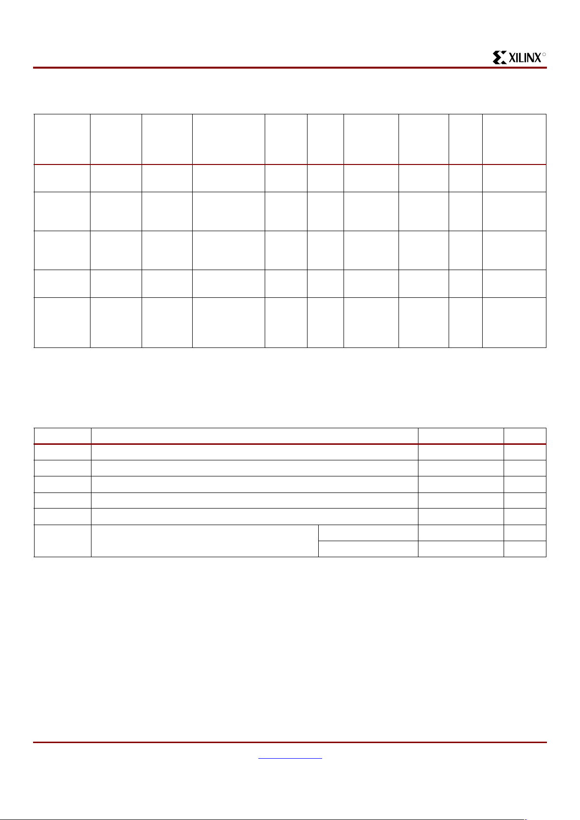
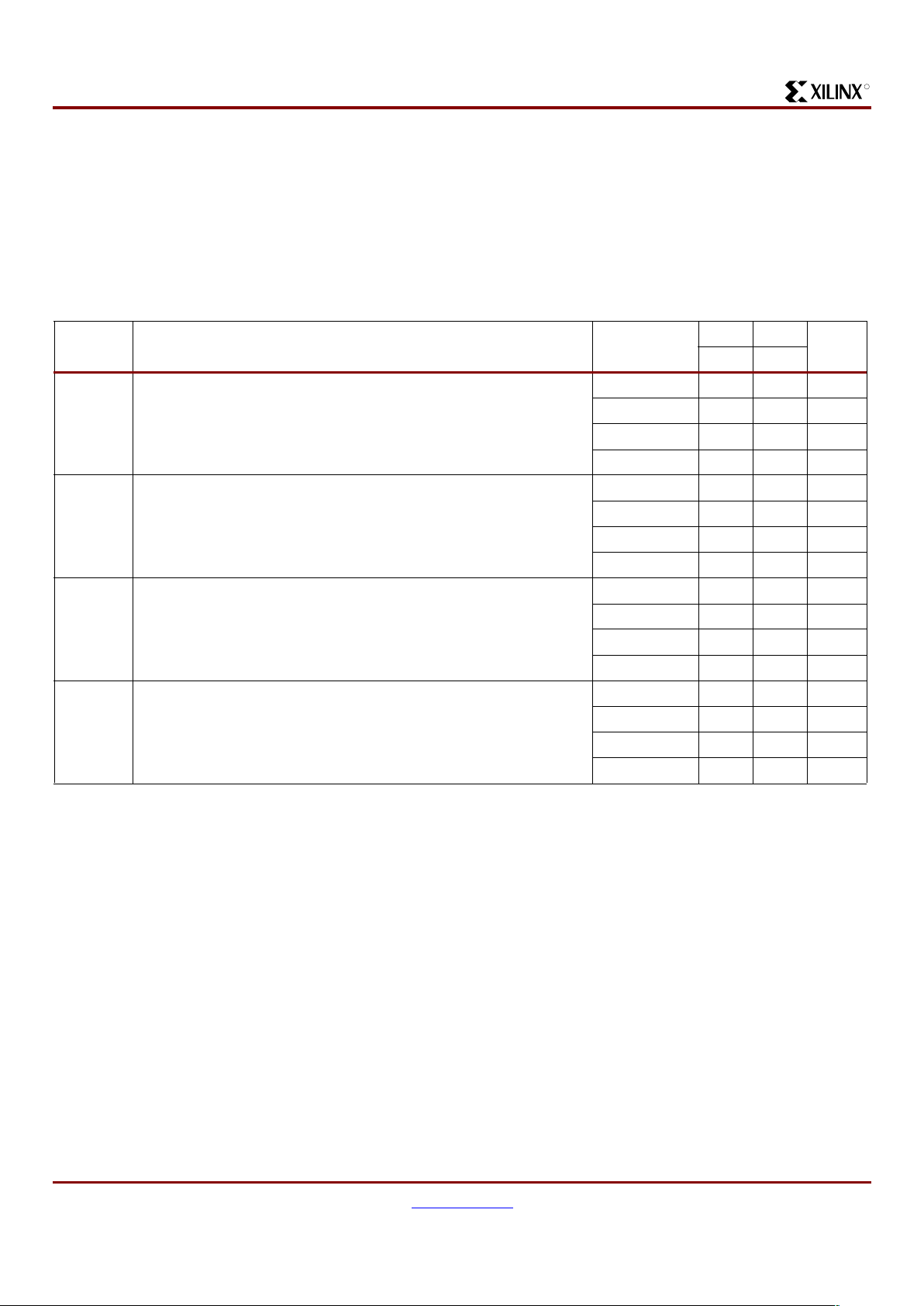
Table 1: XQ4000E/ EX Field Progr ammab le Gate Array s
Device
Max.
Logic
Gates
(No RAM)
Max.
RAM Bits
(No
Logic)
Typical
Gate Range
(Logic and
RAM)
(1)
CLB
Matrix
Total
CLBs
Number
of
Flip-Flops
Max.
Decode
Inputs
per Side
Max.
User
I/O Packages
XQ4005E 5,000 6,272 3,000 - 9,000 14 x 14 196 616 42 112 PG156,
CB164
XQ4010E 10,000 12,800 7,000 - 20,000 20 x 20 400 1,120 60 160 PG191,
CB196,
HQ208
XQ4013E 13,000 18,432 10,000 - 30,000 24 x 24 576 1,536 72 192 PG223,
CB228,
HQ240
XQ4025E 25,000 32,768 15,000 - 45,000 32 x 32 1,024 2,560 96 256 PG299,
CB228
XQ4028EX 28,000 32,768 18,000 - 50,000 32 x 32 1,024 2,560 96 256 PG299,
CB228,
HQ240,
BG352
Notes:
1. Max values of Typ ical Gate Range include 20- 30% of CLBs used as RAM.
Symbol Description Units
V
CC
Supply voltage relative to GND –0.5 to +7.0 V
V
IN
Input voltage relative to GND
(2)
–0.5 to VCC + 0.5 V
V
TS
Voltage applied to High-Z output
(2)
–0.5 to VCC + 0.5 V
T
STG
Storage temperature (ambient) –65 to +150 °C
T
SOL
Maximum soldering temperature (10s @ 1/16 in. = 1.5 mm) +260 °C
T
J
Junction temperature Ceramic package +150 °C
Plastic package +125 °C
Notes:
1. Stresses beyond those listed under Absolu te Maximum Ratings may cause permanent damage to the device. These are str ess
ratings only, and functional operat ion of the device at these or any other conditions beyon d those listed under Operat ing Conditions
is not implied. Exposure to Absolute Maximum Ratings conditions for extended periods of time may affect device reliability.
2. Maximum DC excursion a bov e V
CC
or below Ground must be limited t o ei ther 0.5V or 10 mA, whi chever is easier to achieve . During
transitions, the device pins may undershoot to –2.0V or overshoot to V
CC
+ 2.0V, provided this over or undershoot lasts less than
10 ns and with the forcing current being limited to 200 mA.
QPRO XQ4000E/EX QML High-Reliability FPGAs
DS021 (v2.2) June 25, 2000 www.xilinx.com 3
Product Specification 1-800-255-7778
R
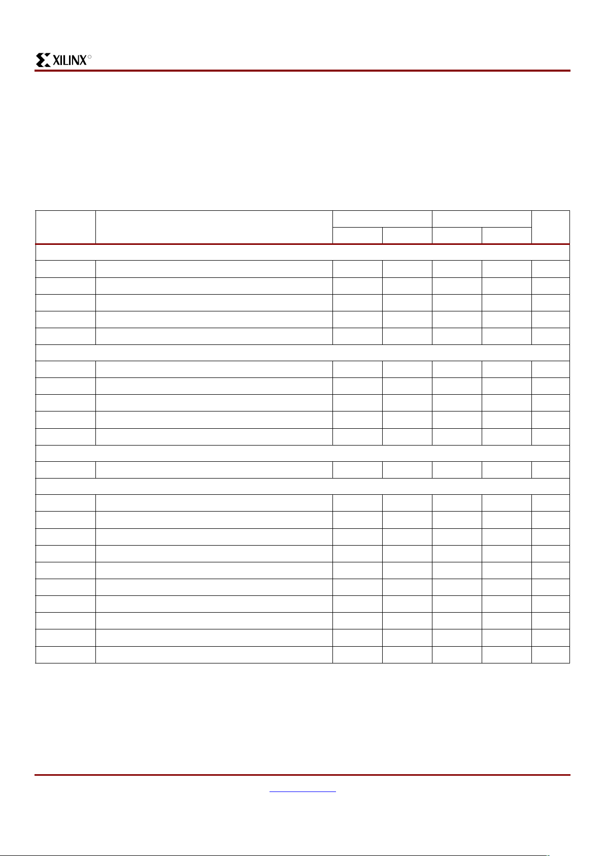
XQ4000E Recommended Operating Conditions
(1,2)
XQ4000E DC Characteristics Over Recommended Operating Conditions
Symbol Description Min Max Units
V
CC
Supply voltage relative to GND, TJ = –55°C to +125°CPlastic 4.5 5.5 V
Supply voltage relative to GND, T
C
= –55°C to +125°C Ceramic 4.5 5.5 V
V
IH
High-Level Input Voltage TTL inputs 2.0 V
CC
V
CMOS inputs 70% 100% V
CC
V
IL
Low-Level Input Voltage TTL inputs 0 0.8 V
CMOS inputs 0 20% V
CC
T
IN
Input signal transition time - 250 ns
Notes:
1. At junction temperatures above those l isted as Operating Condi tions, all delay parameter s increase by 0.35% per °C.
2. Input and output measurement thr eshold are 1.5V for TTL and 2.5V for CMOS.
Symbol Description Min Max Units
V
OH
High-level output voltage @ IOH = –4.0 mA, VCC min TTL outputs 2.4 - V
High-level output voltage @ I
OH
= –1.0 mA, VCC min CMOS outputs VCC – 0.5 - V
V
OL
Low-lev el output voltage @ IOL = 12.0 mA, VCC min
(1)
TTL outputs - 0.4 V
CMOS outputs - 0.4 V
I
CCO
Quiescent FPGA supply current
(2)
-50mA
I
L
Input or output leakage current –10 +10 µA
C
IN
Input capacitance (sample tested) - 16 pF
I
RIN
Pad pull-up (when selected) at VIN = 0V (sample tested)
(3)
–0.02 –0.25 mA
I
RLL
Horizontal longline pull-up (when selected) at logic Low
(3)
0.2 2.5 mA
Notes:
1. With 50% of the outputs simultaneously sinking 12 mA, up to a maximum of 64 pins.
2. With no output cu rrent loads , no a ctiv e input or Longli ne pul l-up resist ors , a ll pa c kage pi ns a t V
CC
or GND, and the FPGA configured
with the dev elopment system Tie opti on.
3. Characterized Only.
QPRO XQ4000E/EX QML High-Reliability FPGAs
4 www.xilinx.com DS021 (v2.2) June 25, 2000
1-800-255-7778 Product Specification
R
XQ4000E Switching Characteristic Guidelines
Testing of the switching parameters is modeled after testing
methods specified by MIL-M-38510/605. All devices are
100% functionally tested. Internal timing parameters are
derived from measuri ng i nter n al tes t patter ns. Listed below
are representative values where one global clock input
drives one vertical clock line in each accessibl e column, and
where all accessible IOB and CLB flip-flops are cl ocked by
the global clock net.
When fewer vertical clock lines are connected, the clock distribution is faster; when multiple clock lines per column are
driven from the same global c lock, the delay is longer. For
more specific, more precise, and worst-case guaranteed
data, reflecting the actual routing struc ture, use the values
provided by the static timing analyzer (TRCE in the Xilinx
Development System) and back-annotated to the simulation
netlist. These path delays, provided as a guideline, have
been extracted from the static timing analyzer report. All
timing parameters assume worst-case operating conditions
(supply voltage and junction temperature).
Note: -3 Speed Grade only applies to XQ4010E and
XQ4013E Plastic Package options only. -4 Speed Grade
applies to all XQ devices and is only available in
Ceramic Packages only.
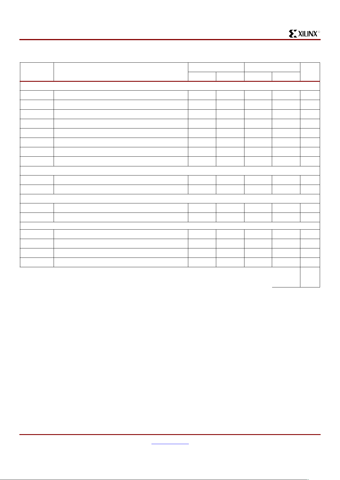
XQ4000E Global Buffer Switching Characteristics
Symbol Description Device
-3
(1)
-4
(2)
UnitsMax Max
T
PG
From pad through primary buffer, to any clock K XQ4005E - 7.0 ns
XQ4010E 6.3 11.0 ns
XQ4013E 6.8 11.5 ns
XQ4025E - 12.5 ns
T
SG
From pad through secondary buffer, to any clock K XQ4005E - 7.5 ns
XQ4010E 6.8 11.5 ns
XQ4013E 7.3 12.0 ns
XQ4025E - 13.0 ns
Notes:
1. For plastic package options only.
2. For ceramic package options only.
QPRO XQ4000E/EX QML High-Reliability FPGAs
DS021 (v2.2) June 25, 2000 www.xilinx.com 5
Product Specification 1-800-255-7778
R
XQ4000E Horizontal Longline Switching Characteristic Guidelines
Testing of switching parameters is modeled after testing
methods specified by MIL-M-38510/605. All devices are
100% functionally tested. Internal timing parameters are
derived from measuri ng i nter n al tes t patter ns. Listed below
are representative values. For more specific, more precise,
and worst-case guaranteed data, use t he values reported
by the static timing analyzer (TRCE i n the X ilinx Development System) and back-annotated t o t he simulation net list.
These path delays, provided as a guideline, have been
extracted from the static timing analyzer report. All timing
parameters assume worst-case operating conditions (supply voltage and junction tempe rature). Values apply to all
XQ4000E devices unless otherwise noted.
The following guidelines reflect worst-case values over the
recommended operating conditions.
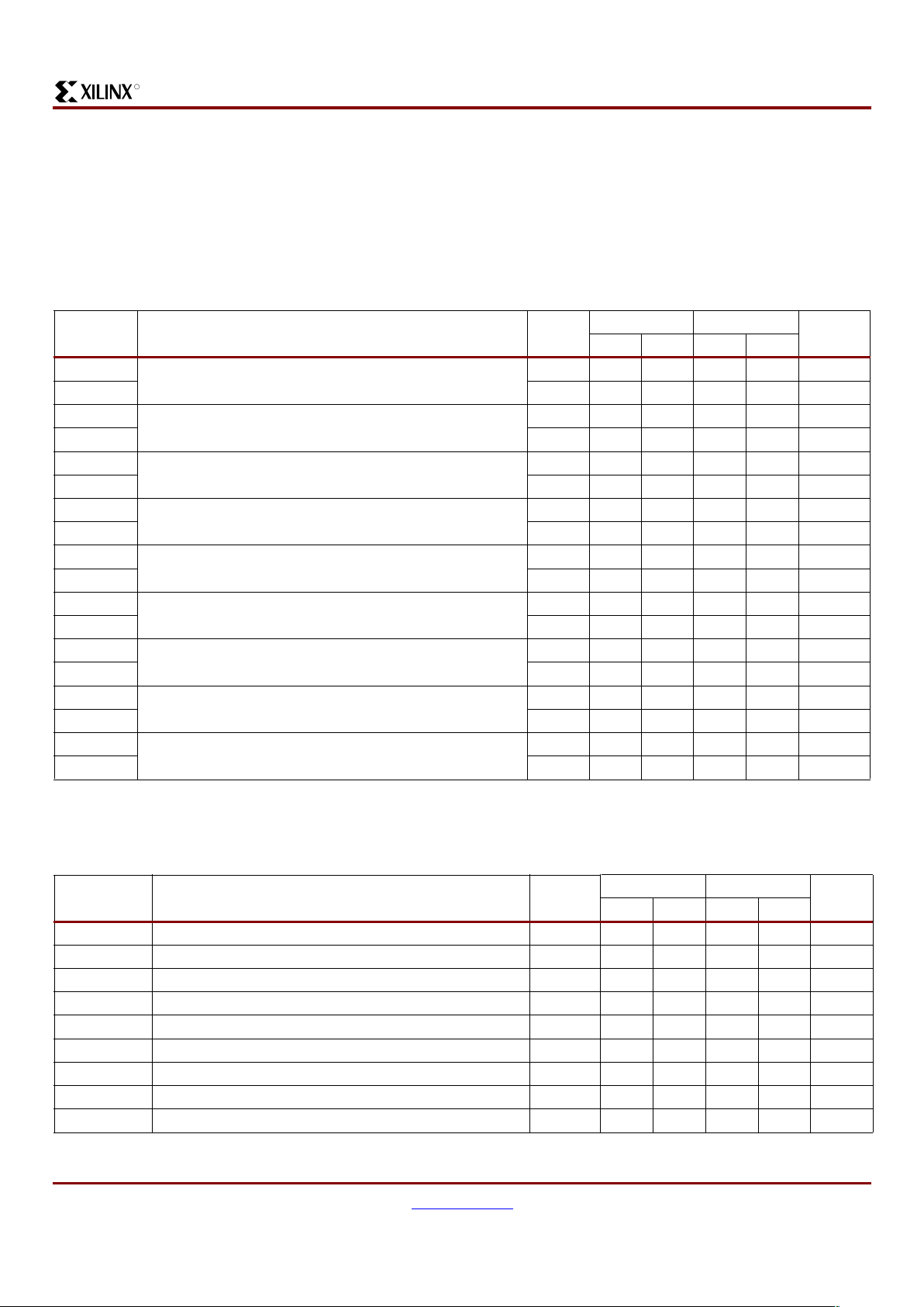
Symbol Description Device
-3 -4
UnitsMax Max
TBUF Driving a Horizontal Longline (LL) :
T
IO1
I going High or Low to LL going High or Low, while T is Low.
Buffer is constantly active.
(1)
XQ4005E - 5.0 ns
XQ4010E 6.4 8.0 ns
XQ4013E 7.2 9.0 ns
XQ4025E - 11.0 ns
T
IO2
I going Low to LL going from resistive pull-up High to active Low.
TBUF configured as open-drain.
(1)
XQ4005E - 6.0 ns
XQ4010E 6.9 10.5 ns
XQ4013E 7.7 11.0 ns
XQ4025E - 12.0 ns
T
ON
T going Low to LL going from resistive pull-up or floating High to
active Low. TBUF configured as open-drain or active buffer with
I=Low.
(1)
XQ4005E - 7.0 ns
XQ4010E 7.3 8.5 ns
XQ4013E 7.5 8.7 ns
XQ4025E - 11.0 ns
T
OFF
T going High to TBUF going inactive, not driving LL. XQ4005E - 1.8 ns
XQ4010E 1.5 1.8 ns
XQ4013E 1.5 1.8 ns
XQ4025E - 1.8 ns
T
PUS
T going High to LL going from Low to High, pulled up by a single
resistor.
(1)
XQ4005E - 23.0 ns
XQ4010E 22.0 29.0 ns
XQ4013E 26.0 32.0 ns
XQ4025E - 42.0 ns
T
PUF
T going High to LL going from Low to High, pulled up by two
resistors.
(1)
XQ4005E - 10.0 ns
XQ4010E 11.0 13.5 ns
XQ4013E 13.0 15.0 ns
XQ4025E - 18.0 ns
Notes:
1. These values include a minimum load. Use the static timing analyzer t o determine the delay for each destinat ion.
QPRO XQ4000E/EX QML High-Reliability FPGAs
6 www.xilinx.com DS021 (v2.2) June 25, 2000
1-800-255-7778 Product Specification
R
XQ4000E Wide Decoder Switching Characteristic Guidelines
Testing of switching parameters is modeled after testing
methods specified by MIL-M-38510/605. All devices are
100% functionally tested. Internal timing parameters are
derived from measuri ng i nter n al tes t patter ns. Listed below
are representative values. For more specific, more precise,
and worst-case guaranteed data, use t he values reported
by the static timing analyzer (TRCE i n the X ilinx Development System) and back-annotated t o t he simulation net list.
These path delays, provided as a guideline, have been
extracted from the static timing analyzer report. All timing
parameters assume worst-case operating conditions (supply voltage and junction tempe rature). Values apply to all
XQ4000E devices unless otherwise noted.
The following guidelines reflect worst-case values over the
recommended operating conditions.
Symbol Description
(1,2)
Device
-3 -4
UnitsMax Max
T
WAF
Full length, both pull-ups, inputs from IOB I-pins XQ4005E - 9. 5 ns
XQ4010E 9.0 15.0 ns
XQ4013E 11.0 16.0 ns
XQ4025E - 18.0 ns
T
WAFL
Full length, both pull-ups, inputs from internal logic XQ4005E - 12.5 ns
XQ4010E 11.0 18.0 ns
XQ4013E 13.0 19.0 ns
XQ4025E - 21.0 ns
T
WAO
Half length, one pull-up, inputs from IOB I-pins XQ4005E - 10.5 ns
XQ4010E 10.0 16.0 ns
XQ4013E 12.0 17.0 ns
XQ4025E - 19.0 ns
T
WAOL
Half length, one pull-up, inputs from internal logic XQ4005E - 12.5 ns
XQ4010E 12.0 18.0 ns
XQ4013E 14.0 19.0 ns
XQ4025E - 21.0 ns
Notes:
1. These delays are specified from the decoder input to the decoder output.
2. Fewer than t he specified numbe r of pull-up resistors can be used, if desi red. Using fewer pull-ups reduces powe r consumption but
increases delays. Use the static timing analyzer to determine delays if fewer pull-ups are used.
QPRO XQ4000E/EX QML High-Reliability FPGAs
DS021 (v2.2) June 25, 2000 www.xilinx.com 7
Product Specification 1-800-255-7778
R
XQ4000E CLB Switching Characteristic Guidelines
Testing of switching parameters is modeled after testing
methods specified by MIL-M-38510/605. All devices are
100% functionally tested. Internal timing parameters are
derived from measuri ng i nter n al tes t patter ns. Listed below
are representative values. For more specific, more precise,
and worst-case guaranteed data, use t he values reported
by the static ti ming analyzer (TR CE in the Xilinx Development System) and back-annotated to the simulation netlist.
These path delays, provided as a guideline, have been
extracted from the static timing analyzer report. All timing
parameters assume worst-case operating conditions (supply voltage and junction tempe rature). Values apply to all
XQ4000E devices unless otherwise noted.
Symbol Description
-3 -4
UnitsMin Max Min Max
Combinatorial Delays
T
ILO
F/G inputs to X/Y outputs - 2. 01 - 2.7 ns
T
IHO
F/G inputs via H to X/Y outputs - 4.3 - 4.7 ns
T
HH0O
C inputs via SR through H to X/Y outputs - 3.3 - 4.1 ns
T
HH1O
C inputs via H to X/Y outputs - 3.6 - 3.7 ns
T
HH2O
C inputs via DIN through H to X/Y outputs - 3.6 - 4.5 ns
CLB Fast Carry Logic
T
OPCY
Operand inputs (F1, F2, G1, G4) to C
OUT
-2.6-3.2ns
T
ASCY
Add/Subtract input (F3) to C
OUT
-4.4-5.5ns
T
INCY
Initialization inputs (F1, F3) to C
OUT
-1.7-1.7ns
T
SUM
CIN through function generators to X/Y outputs - 3.3 - 3.8 ns
T
BYP
C
IN
to C
OUT
, bypass function generators - 0.7 - 1.0 ns
Sequential Delays
T
CKO
Clock K to outputs Q - 2.8 - 3.7 ns
Setup Time before Clock K
T
ICK
F/G inputs 3.0 - 4. 0 - ns
T
IHCK
F/G in puts via H 4.6 - 6.1 - ns
T
HH0CK
C inputs via H0 through H 3.6 - 4.5 - ns
T
HH1CK
C inputs via H1 through H 4.1 - 5.0 - ns
T
HH2CK
C inputs via H2 through H 3.8 - 4.8 - ns
T
DICK
C inputs via D
IN
2.4 - 3. 0 - ns
T
ECCK
C inputs via EC 3.0 - 4.0 - ns
T
RCK
C inputs via S/R, going Low (inactive) 4.0 - 4.2 - ns
T
CCK
CIN input via F/G 2.1 - 2. 5 - ns
T
CHCK
CIN input via F/G and H 3.5 - 4. 2 - ns
QPRO XQ4000E/EX QML High-Reliability FPGAs
8 www.xilinx.com DS021 (v2.2) June 25, 2000
1-800-255-7778 Product Specification
R
XQ4000E CLB Switching Characteristic Guidelines (continued)
Symbol
Description
-3 -4
UnitsMin Max Min Max
Hold Time after Clock K
T
CKI
F/G inputs 0 - 0 - n s
T
CKIH
F/G inputs via H 0 - 0 - n s
T
CKHH0
C inputs via H0 through H 0 - 0 - ns
T
CKHH1
C inputs via H1 through H 0 - 0 - ns
T
CKHH2
C inputs via H2 through H 0 - 0 - ns
T
CKDI
C inputs via DIN/H2 0 - 0 - ns
T
CKEC
C inputs via EC 0 - 0 - ns
T
CKR
C inputs via SR, going Low (inactive) 0 - 0 - ns
Clock
T
CH
Clock High time 4.0 - 4.5 - ns
T
CL
Clock Low time 4.0 - 4.5 - ns
Set/Reset Direct
T
RPW
Width (High) 4.0 - 5.5 - ns
T
RIO
Delay from C inputs via S/R, going High to Q - 4.0 - 6.5 ns
Master Set/Reset
(1)
T
MRW
Width (High or Low) 11. 5 - 13.0 - ns
T
MRQ
Delay from Global Set/Reset net to Q - 18.7 - 23.0 ns
T
MRK
Global Set/Reset inactive to first active clock K edge - 18.7 - 23.0 ns
F
TOG
Toggle Frequency
(2)
- 125 - 111 MHz
Notes:
1. Timing is based on the XC4005E. For other devices see the static timing analyzer.
2. Export Control Max. flip-flop toggle rate.
QPRO XQ4000E/EX QML High-Reliability FPGAs
DS021 (v2.2) June 25, 2000 www.xilinx.com 9
Product Specification 1-800-255-7778
R
XQ4000E CLB Edge-Triggered (Synchro nous) RAM Switching Characteristic Guidelines
Testing of switching parameters is modeled after testing
methods specified by MIL-M-38510/605. All devices are
100% functionally tested. Internal timing parameters are
derived from measuri ng i nter n al tes t patter ns. Listed below
are representative values. For more specific, more precise,
and worst-case guaranteed data, use t he values reported
by the static timing analyzer (TRCE in the Xilinx Development System) an d back-ann otated to th e simu lation n etlist.
All timing parameters ass ume worst-case operating con ditions (supply voltage and junction temperature). Values
apply to all XQ4000E/EX devices unless otherwise noted.
Single-Port RAM Synchronous (Edge-Triggered) Write Operation Characteristics
Symbol Write Operation Description Size
-3 -4
UnitsMin Max Min Max
T
WCS
Address write cycle time (clock K period) 16x2 14.4 - 15.0 - ns
T
WCTS
32x1 14.4 - 15.0 - ns
T
WPS
Clock K pulse width (active edge) 16x2 7.2 1 ms 7.5 1 ms ns
T
WPTS
32x1 7.2 1 ms 7 .5 1 ms ns
T
ASS
Address setup time before clock K 16x2 2.4 - 2.8 - ns
T
ASTS
32x1 2. 4 - 2.8 - ns
T
AHS
Address hold time after clock K 16x2 0 - 0 - ns
T
AHTS
32x1 0 - 0 - ns
T
DSS
DIN setup time before clock K 16x2 3.2 - 3.5 - ns
T
DSTS
32x1 1. 9 - 2.5 - ns
T
DHS
D
IN
hold time after clock K 16x 2 0 - 0 - ns
T
DHTS
32x1 0 - 0 - ns
T
WSS
WE setup time before clock K 16x2 2.0 - 2 .2 - ns
T
WSTS
32x1 2. 0 - 2.2 - ns
T
WHS
WE hold time after clock K 16x2 0 - 0 - ns
T
WHTS
32x1 0 - 0 - ns
T
WOS
Data valid after clock K 16x2 8.8 - - 10.3 ns
T
WOTS
32x1 10.3 - - 11.6 ns
Notes:
1. Timing for the 16x1 RAM option is identical to 16x2 RAM timing.
2. Applicable Read timing specifications are ide ntical to Level-Sensitive Read timing.
Dual-Port RAM Synchronous (Edge-Triggered) Write Operation Characteristics
Symbol Write Operation Description Size
(1)
-3 -4
UnitsMin Max Min Max
T
WCDS
Address write cycle time (clock K period) 16x1 14.4 15.0 ns
T
WPDS
Clock K pulse width (active edge) 16x1 7.2 1 ms 7.5 1 ms ns
T
ASDS
Address setup time before clock K 16x1 2.5 - 2.8 - ns
T
AHDS
Address hold time after clock K 16x1 0 - 0 - ns
T
DSDS
DIN setup time before clock K 16x1 2. 5 - 2.2 - ns
T
DHDS
DIN hold time after clock K 16x1 0 - 0 - ns
T
WSDS
WE setup time before clock K 16x1 1.8 - 2.2 - ns
T
WHDS
WE hold time after clock K 16x1 0 - 0.3 - ns
T
WODS
Data valid after clock K 16x1 - 7.8 - 10.0 ns
Notes:
1. Applicable Read timing specifications are ide ntical to Level-Sensitive Read timing.
QPRO XQ4000E/EX QML High-Reliability FPGAs
10 www.xilinx.com DS021 (v2.2) June 25, 2000
1-800-255-7778 Product Specification
R
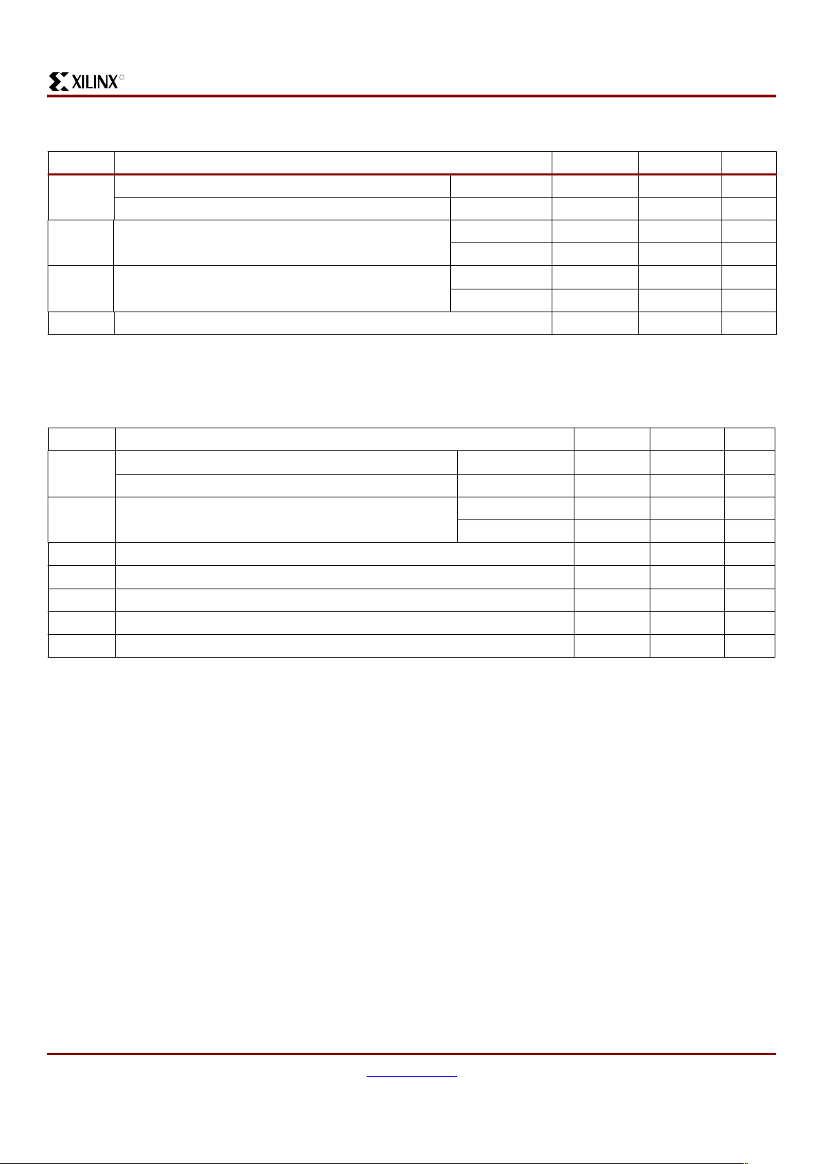
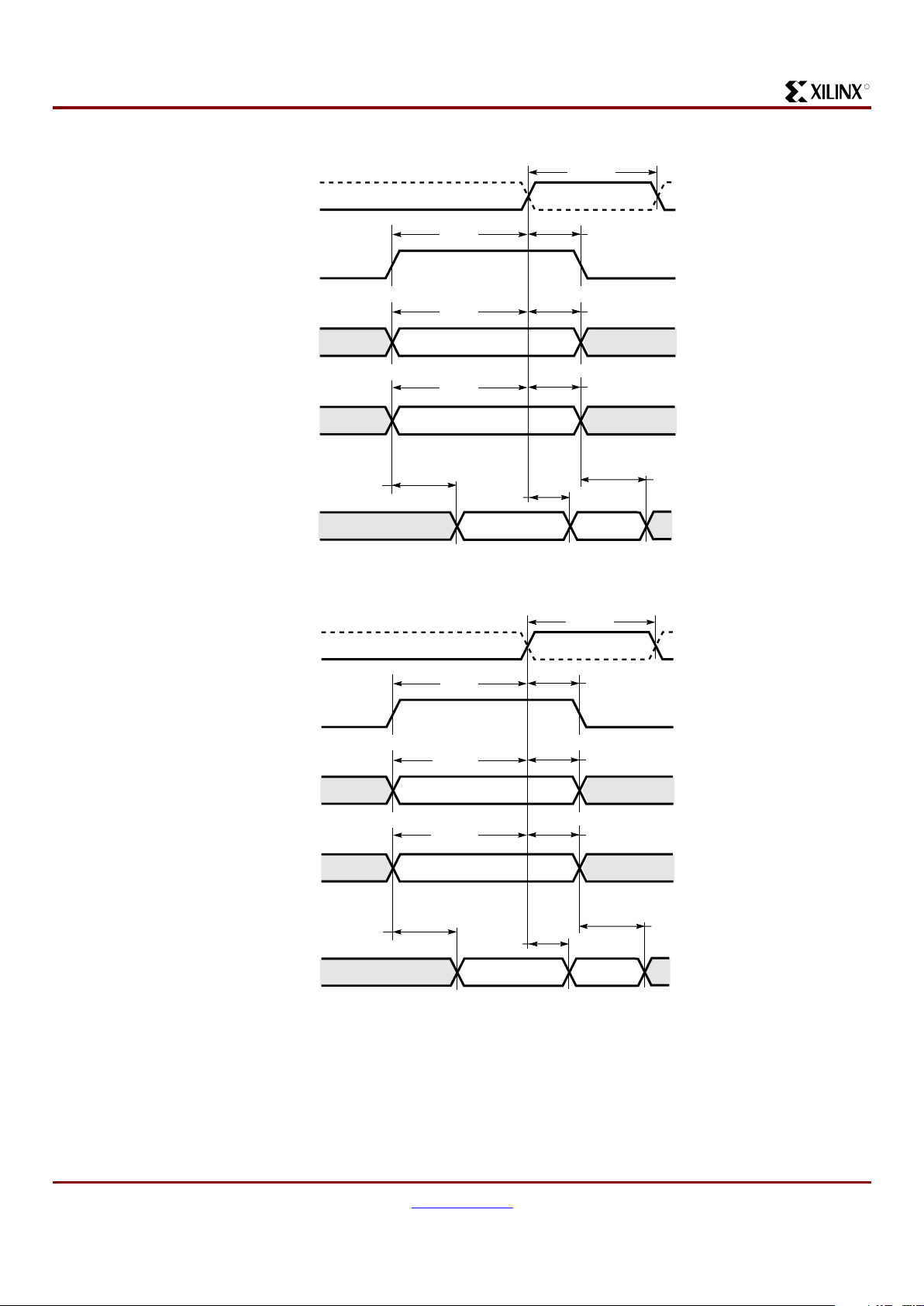
XQ4000E CLB RAM Synchronous (Edge-Triggered) Write Timing Waveform
XQ4000E CLB Dual-Port RAM Synchronous (Edge-Triggered) Write Timing Waveform
DS021_01_060100
WCLK (K)
WE
ADDRESS
DATA IN
DATA OUT
OLD NEW
T
DSS
T
DHS
T
ASS
T
AHS
T
WSS
T
WPS
T
WHS
T
WOS
T
ILO
T
ILO
DS021_02_060100
WCLK (K)
WE
ADDRESS
DATA IN
DATA OUT
OLD NEW
T
DSDS
T
DHDS
T
ASDS
T
AHDS
T
WSS
T
WPDS
T
WHS
T
WODS
T
ILO
T
ILO
QPRO XQ4000E/EX QML High-Reliability FPGAs
DS021 (v2.2) June 25, 2000 www.xilinx.com 11
Product Specification 1-800-255-7778
R
XQ4000E CLB Level-Sensitive RAM Switching Characteristic Guidelines
Testing of switching parameters is modeled after testing
methods specified by MIL-M-38510/605. All devices are
100% functionally tested. Internal timing parameters are
derived from measuri ng i nter n al tes t patter ns. Listed below
are representative values. For more specific, more precise,
and worst-case guaranteed data, use t he values reported
by the static timing analyzer (TRCE in the Xilinx Development System) an d back-ann otated to th e simu lation n etlist.
All timing parameters ass ume worst-case operating con ditions (supply voltage and junction temperature). Values
apply to all XQ4000E devices unless otherwise noted.
Symbol Single Port RAM Size
-3 -4
UnitsMin Max Min Max
Write Operation
T
WC
Address write cycle time 16x2 8.0 - 8 .0 - ns
T
WCT
32x1 8. 0 - 8.0 - ns
T
WP
Write Enable pulse width (High) 16x2 4.0 - 4.0 - ns
T
WPT
32x1 4. 0 - 4.0 - ns
T
AS
Address setup time before WE 16x2 2.0 - 2.0 - ns
T
AST
32x1 2. 0 - 2.0 - ns
T
AH
Address hold time after end of WE 16x2 2.0 - 2.5 - ns
T
AHT
32x1 2. 0 - 2.0 - ns
T
DS
DIN setup time before end of WE 16x2 2.2 - 4 .0 - ns
T
DST
32x1 2. 2 - 5.0 - ns
T
DH
DIN hold time after end of WE 16x2 2.0 - 2.0 - ns
T
DHT
32x1 2. 0 - 2.0 - ns
Read Operation
T
RC
Address read cycle time 16x2 3.1 - 4.5 - ns
T
RCT
32x1 5. 5 - 6.5 - ns
T
ILO
Data valid after address change (no Write Enable) 16x2 - 1.8 - 2.7 ns
T
IHO
32x1 - 3.2 - 4.7 ns
Read Operation, Clocking Data into Flip-Flop
T
ICK
Address setup time before clock K 16x2 3.0 - 4.0 - ns
T
IHCK
32x1 4. 6 - 6.1 - ns
Read During Write
T
WO
Data valid after WE goes active (DIN stable before WE) 16x2 - 6.0 - 10.0 ns
T
WOT
32x1 - 7.3 - 12.0 ns
T
DO
Data valid after DIN (DIN changes during WE) 16x2 - 6.6 - 9.0 ns
T
DOT
32x1 - 7.6 - 11.0 ns
Read During Write, Clocking Data into Flip-Flop
T
WCK
WE setup time before clock K 16x2 6.0 - 8 .0 - ns
T
WCKT
32x1 6. 8 - 9.6 - ns
T
DCK
Data setup time before clock K 16x2 5.2 - 7.0 - ns
T
DOCK
32x1 6. 2 - 8.0 - ns
Notes:
1. Timing for the 16x1 RAM option is identical to 16x2 RAM timing.

QPRO XQ4000E/EX QML High-Reliability FPGAs
12 www.xilinx.com DS021 (v2.2) June 25, 2000
1-800-255-7778 Product Specification
R
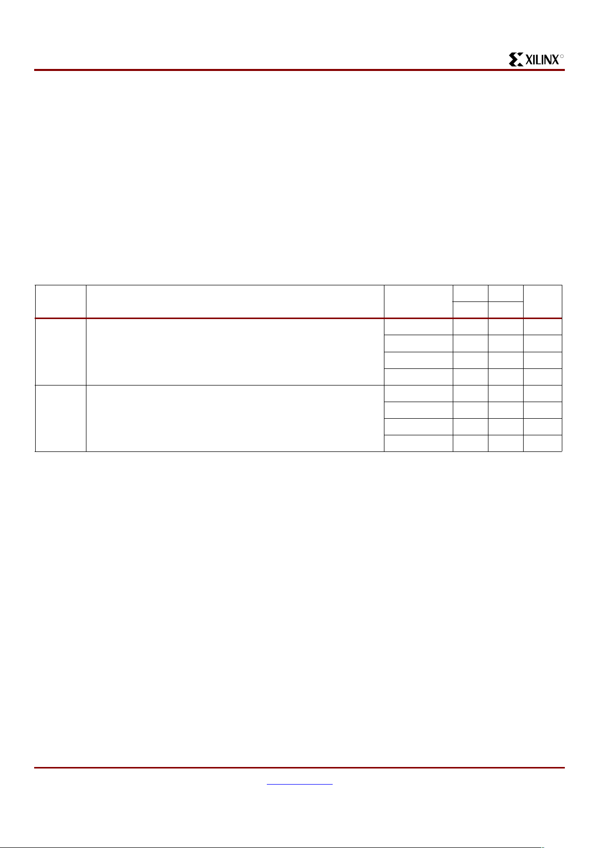
XQ4000E CLB Level-Sensitive RAM Timing Characteristics
DS021_03_060100
WE
ADDRESS
WRITE
READ WITHOUT WRITE
READ, CLOCKING DATA INTO FLIP-FLOP
READ DURING WRITE, CLOCKING DATA INTO FLIP-FLOP
READ DURING WRITE
DATA IN
CLOCK
XQ,YQ OUTPUTS
WRITE ENABLE
DATA IN
(stable during WE)
WRITE ENABLE
DATA IN
CLOCK
DATA IN
(changing during WE)
X,Y OUTPUTS
VALID
VALID
OLD NEW
VALID
VALID (NEW)VALID (OLD)
VALID
T
AS
T
ILO
T
AH
T
DS
REQUIRED
T
DH
T
WP
T
WC
T
ICK
T
CH
T
CKO
X,Y OUTPUTS
X,Y OUTPUTS
XQ,YQ OUTPUTS
T
DH
T
WO
T
WO
T
DO
T
WCK
T
DCK
T
CKO
T
WP
T
WP
VALID
(OLD)
VALID
(PREVIOUS)
VALID
(NEW)

QPRO XQ4000E/EX QML High-Reliability FPGAs
DS021 (v2.2) June 25, 2000 www.xilinx.com 13
Product Specification 1-800-255-7778
R
XQ4000E Guaranteed Input and Output Parameters (Pin-to-Pin, TTL I/O)
Testing of switching parameters is modeled after testing
methods specified by MIL-M-38510/605. All devices are
100% functionally tested. Pin-to-pin timing parameters are
derived from measuring external and inter nal test patterns
and are guaranteed over worst-case operating conditions
(supply voltage and junction temperature). Listed below are
representative values for typical pin locations and nor mal
clock loading. For more specific, more precise, and
worst-case guaranteed data, reflecting the actual routing
structure, use the values provided by the static timing analyzer (TRCE in the Xilinx Development System) and
back-annotated to the simulation netlist. These path delays,
provided as a guideline, have been extracted from the static
timing analyzer report. Values apply to all XQ4000E devices
unless otherwise noted.
Symbol Description D evice -3 -4 Units
T
ICKOF
(Max)
Global clock to output (fast) using OFF XQ4005E - 14.0 ns
XQ4010E 10.9 16.0 ns
XQ4013E 11.0 16.5 ns
XQ4025E - 17.0 ns
T
ICKO
(Max)
Global clock to output (slew-limited) using OFF X Q4005E - 18.0 ns
XQ4010E 14.9 20.0 ns
XQ4013E 15.0 20.5 ns
XQ4025E - 21.0 ns
T
PSUF
(Min)
Input setup time, using IFF (no delay) XQ4005E - 2.0 ns
XQ4010E 0.2 1.0 ns
XQ4013E 0 0.5 ns
XQ4025E - 0 ns
T
PHF
(Min)
Input hold time, using IFF (no delay) XQ4005E - 4.6 ns
XQ4010E 5.5 6.0 ns
XQ4013E 6.5 7.0 ns
XQ4025E - 8.0 ns
T
PSU
(Min)
Input setup time, using IFF (with delay) XQ4005E - 8.5 ns
XQ4010E 7.0 8.5 ns
XQ4013E 7.0 8.5 ns
XQ4025E - 9.5 ns
T
PH
(Min)
Input hold time, using IFF (with delay) XQ4005E - 0 ns
XQ4010E 0 0 ns
XQ4013E 0 0 ns
XQ4025E - 0 ns
Notes:
1. OFF = Output Flip-Flop
2. IFF = Input Flip-Flop or Latch
OFF
T
PG
Global Clock-to-Output Delay
DS021_04_060100
OFF
T
PG
Global Clock-to-Output Delay
DS021_04_060100
IFF
T
PG
D
Input
Setup
and Hold
Time
DS021_05_060100
IFF
T
PG
D
Input
Setup
and Hold
Time
DS021_05_060100
IFF
T
PG
D
Input
Setup
and Hold
Time
DS021_05_060100
IFF
T
PG
D
Input
Setup
and Hold
Time
DS021_05_060100

QPRO XQ4000E/EX QML High-Reliability FPGAs
14 www.xilinx.com DS021 (v2.2) June 25, 2000
1-800-255-7778 Product Specification
R
XQ4000E IOB Input Switching Characteristic Guidelines
Testing of switching parameters is modeled after testing
methods specified by MIL-M-38510/605. All devices are
100% functionally tested. Pin-to-pin timing parameters are
derived from measuring external and inter nal test patterns
and are guaranteed over worst-case operating conditions
(supply voltage and junction temperature). Listed below are
representative values for typical pin locations and nor mal
clock loading. For more specific, more precise, and
worst-case guaranteed data, reflecting the actual routing
structure, use the values provided by the static timing analyzer (TRCE in the Xilinx Development System) and
back-annotated to the simulation netlist. These path delays,
provided as a guideline, have been extracted from the static
timing analyzer report. Values apply to all XQ4000E devices
unless otherwise noted.
Symbol Description Device
-3 -4
UnitsMin Max Min Max
Propagation Delays (TTL Inputs)
(1)
T
PID
Pad to I1, I2 All devices - 2. 5 - 3.0 ns
T
PLI
Pad to I1, I2 via transparent input latch, no delay All devices - 3.6 - 4.8 ns
T
PDLI
Pad to I1, I2 via transparent FCL and input latch,
with delay
XQ4005E - - - 10.8 ns
XQ4010E - 10.8 - 11.0 ns
XQ4013E - 11.2 - 11.4 ns
XQ4025E - - - 13.8 ns
Propagation Delays (CMOS Inputs)
(1)
T
PIDC
Pad to I1, I2 All devices - 4. 1 - 5.5 ns
T
PLIC
Pad to I1, I2 via transparent input latch, no delay All devices - 8.8 - 6.8 ns
T
PDLIC
Pad to I1, I2 via transparent FCL and input latch,
with delay
XQ4005E - - - 16.5 ns
XQ4010E - 14.0 - 17.5 ns
XQ4013E - 14.4 - 18.0 ns
XQ4025E - - - 20.8 ns
Propagation Delays (TTL Inputs)
T
IKRI
Clock (IK) to I1, I2 (flip-flop) All devices - 2.8 - 5.6 ns
T
IKLI
Clock (IK) to I1, I2 (latch enable, active Low) All devices - 4.0 - 6.2 ns
Hold Times
(2)
T
IKPI
Pad to clock (IK), no delay All devices 0 - 0 - ns
T
IKPID
Pad to clock (IK), with delay All devices 0 - 0 - ns
T
IKEC
Clock enable (EC) to clock (K), no delay All devices 1.5 - 1.5 - ns
T
IKECD
Clock enable (EC) to clock (K), with delay All devices 0 - 0 - ns
Notes:
1. Input pad setup and hold ti mes are speci fie d with re spect t o the int ernal cloc k (IK). F or set up and ho ld times wit h respect to the clock
input pin, see the pin- to-pin parameter s in the Guaranteed Input and Output Param eters table.
2. Voltage levels of unused pads, bonded or unbonded, must be valid logic levels. Each can be configured with the internal pull-up
(default) or pull-down resistor, or configured as a driven output, or can be driven from an external source.

QPRO XQ4000E/EX QML High-Reliability FPGAs
DS021 (v2.2) June 25, 2000 www.xilinx.com 15
Product Specification 1-800-255-7778
R
XQ4000E IOB Input Switching Characteristic Guidelines (continued)
Symbol Description Device
-3 -4
UnitsMinMaxMinMax
Setup Times (TTL Inputs)
(1,2)
T
PICK
Pad to clock (IK), no delay All devices 2.6 - 4.0 - ns
T
PICKD
Pad to clock (IK), with delay X Q4005E - - 10.9 - ns
XQ4010E 9.8 - 11.3 - ns
XQ4013E 10.2 - 11.8 - ns
XQ4025E - - 14.0 - ns
Setup Times (CMOS Inputs)
(1,2)
T
PICKC
Pad to clock (IK), no delay All devices 3.3 - 6.0 - ns
T
PICKDC
Pad to clock (IK), with delay X Q4005E - - 12.0 - ns
XQ4010E 10.5 - 13.0 - ns
XQ4013E 10.9 - 13.5 - ns
XQ4025E - - 16.0 - ns
(TTL or CMOS)
T
ECIK
Clock enable (EC) to clock (IK), no delay All devices 2.5 - 3.5 - ns
T
ECIKD
Clock enable (EC) to clock (IK), with delay XQ4005E - - 10.4 - ns
XQ4010E 9.7 - 10.7 - ns
XQ4013E 10.1 - 11.1 - ns
XQ4025E - - 14.0 - ns
Global Set/Reset
(3)
T
RRI
Delay from GSR net through Q to I1, I2 All devices - 7.8 - 12.0 ns
T
MRW
GSR width All devices 11.5 - 13.0 - ns
T
MRI
GSR inactive to first active clock (IK) edge All devices 11.5 - 13.0 - ns
Notes:
1. Input pad setup and hold times ar e speci fied with r esp ect to the i nternal cloc k (IK). F o r setup an d hold ti mes with respe ct to the cloc k
input pin, see the pin- to-pin parameter s in the Guaranteed Input and Output Param eters table.
2. Voltage levels of unused pads, bonded or unbonded, must be valid logic levels. Each can be configured with the internal pull-up
(default) or pull-down resistor, or configured as a driven output, or can be driven from an external source.
3. Timing is based on the XC4005E. For other devices see the XACT timing calculator.

QPRO XQ4000E/EX QML High-Reliability FPGAs
16 www.xilinx.com DS021 (v2.2) June 25, 2000
1-800-255-7778 Product Specification
R
XQ4000E IOB Output Switching Characteristic Guidelines
Testing of switching parameters is modeled after testing
methods specified by MIL-M-38510/605. All devices are
100% functionally tested. Internal timing parameters are
derived from measuri ng i nter n al tes t patter ns. Listed below
are representative values. For more specific, more precise,
and worst-case guaranteed data, use t he values reported
by the static ti ming analyzer (TR CE in the Xilinx Develop-
ment System) an d back-ann otated to th e simu lation n etlist.
These path delays, provided as a guideline, have been
extracted from the static timing analyzer report. All timing
parameters assume worst-case operating conditions (supply voltage and junction temperature). For Propagation
Delays, slew-rate = fast unless otherwise noted. Values
apply to all XQ4000E devices unless otherwise noted.
Symbol Description
-3 -4
UnitsMin Max Min Max
Propagation Delays (TTL Output Levels)
T
OKPOF
Clock (OK) to pad, fast - 6.5 - 7.5 ns
T
OKPOS
Clock (OK) to pad, slew-rate limited - 9.5 - 11.5 ns
T
OPF
Output (O) to pad, fast - 5.5 - 8.0 ns
T
OPS
Output (O) to pad, slew-rate limited - 8.6 - 12.0 ns
T
TSHZ
3-state to pad High-Z, slew-rate independent - 4.2 - 10 .0 ns
T
TSONF
3-state to pad active and valid, fast - 8.1 - 10 .0 ns
T
TSONS
3-state to pad active and valid, slew-rate limited - 11.1 - 13.7 ns
Propagation Delays (CMOS Output Levels)
T
OKPOFC
Clock (OK) to pad, fast - 7.8 - 9.5 ns
T
OKPOSC
Clock (OK) to pad, slew-rate limited - 11. 6 - 13.5 ns
T
OPFC
Output (O) to pad, fast - 9.7 - 10.0 ns
T
OPSC
Output (O) to pad, slew-rate limited - 13.4 - 14.0 ns
T
TSHZC
3-state to pad High-Z, slew-rate independent - 4.3 - 5.2 ns
T
TSONFC
3-state to pad active and valid, fast - 7.6 - 9.1 ns
T
TSONSC
3-state to pad active and valid, slew-rate limited - 11.4 - 13.1 ns
Setup and Hold Times
T
OOK
Output (O) to clock (OK) setup time 4.6 - 5.0 - ns
T
OKO
Output (O) to clock (OK) hold time 0 - 0 - ns
T
ECOK
Clock enable (EC) to clock (OK) setup 3.5 - 4.8 - ns
T
OKEC
Clock enable (EC) to clock (OK) hold 1.2 - 1.2 - ns
Clock
T
CH
Clock High 4.0 - 4.5 - ns
T
CL
Clock Low 4.0 - 4.5 - ns
Global Set/Reset
(3)
T
RRO
Delay from GSR net to pad - 11. 8 - 15.0 ns
T
MRW
GSR width 11.5 - 13.0 - ns
T
MRO
GSR inactive to first active clock (OK) edge 11.5 - 13.0 - ns
Notes:
1. Output timing is measured at pin thr eshold, with 50 pF external capaciti ve loads (incl. test fixture). Sle w-rate limited output rise/fall
times are appr o ximat ely t wo times lon ger th an f ast o utput rise/f al l tim es. F or t he e ff ect of c apacit iv e l oads on g r ound bounce, se e the
“Additional XC4000 Data” secti on on the Xilinx web site , www.xilinx.com/partinfo/databook.htm
.
2. Voltage levels of unused pads, bonded or unbonded, must be valid logic levels. Each can be configured with the internal pull-up
(default) or pull-down resistor, or configured as a driven output, or can be driven from an external source.
3. Timing is based on the XC4005E. For other devices see the XACT timing calculator.

QPRO XQ4000E/EX QML High-Reliability FPGAs
DS021 (v2.2) June 25, 2000 www.xilinx.com 17
Product Specification 1-800-255-7778
R
XC4000E Boundary Scan (JTAG) Switching Characteristic Guidelines
Testing of the switching parameters is modeled after testing
methods specified by MIL-M-38510/605. All devices are
100% functionally tested. Internal timing parameters are not
measured directly . They are derived from benchmark timing
patterns that are taken at device introduction, prior to any
process improvements. For more detailed, more precise,
and more up-to-date information, us e the values provided
by the XACT timing calculator and used in the simulator.
These values can be printed in tabular format by running
LCA2XNF-S.
The following guidelines reflect worst-case values over the
recommended operating conditions. They are expressed in
units of nanoseconds and apply to all XC4000E devices
unless otherwise noted.
-3 -4
UnitsSymbol Description Min Max Min Max
Setup Times
T
TDITCK
Input (TDI) to clock (TCK) 30.0 30.0 ns
T
TMSTCK
Input (TMS) to clock (TCK) 15.0 15.0 ns
Hold Times
T
TCKTDI
Input (TDI) to clock (TCK) 0 0 ns
T
TCKTMS
Input (TMS) to clock (TCK) 0 0 ns
Propagation Delay
T
TCKPO
Clock (TCK) to pad (TDO) 30.0 30.0 ns
Clock
T
TCKH
Clock (TCK) High 5.0 5.0 ns
T
TCKL
Clock (TCK) Low 5.0 5.0 ns
F
MAX
Frequency 15.0 15.0 MHz
Notes:
1. Input setup and hold times and clock-to-pad times are specified with respect to external signal pins.
2. Output timing is measured at pin thr eshold, with 50pF ext ernal capacitiv e loads (incl. test fixture). Slew-r ate limited output rise/fall
times are appr o ximat ely t wo times lon ger th an f ast o utput rise/f al l tim es. F or t he e ff ect of c apacit iv e l oads on gr ound bounce, s ee the
“Additional XC4000 Data” secti on of the Programmab le Logic Data Book.
3. Voltage levels of unused pads, bonded or unbonded, must be valid logic levels. Each can be configured with the internal pull-up
(default) or pull-down resistor, or configured as a driven output, or can be driven from an external source.

QPRO XQ4000E/EX QML High-Reliability FPGAs
18 www.xilinx.com DS021 (v2.2) June 25, 2000
1-800-255-7778 Product Specification
R
XQ4028EX Swit chin g Chara cter ist ics
Definition of Terms
In the following tables, some specifications may be designated as Advance or Preliminary. These term s are defined as
follows:
Advance: Initial estimates based on simulation and/or extrapolation from ot her speed gra des, devices, or device families.
Values are subject to change. Use as estimates, not for production.
Preliminary: Based on preliminary characterizat ion. Further changes are not expected.
Unmarked: Specifications not identified as either Advance or Preliminary are to be considered Final.
Except for pin-to-pin input and output parameters, the A.C. parameter delay specifications included in this document are
derived from measuring internal test patterns. All specifications are representative of worst-case supply voltage and junction
temperature conditions.
All specifications subject to change without notice.
XQ4028EX Absolute Maximum Ratings
(1)
Symbol Description Units
V
CC
Supply voltage relative to GND –0.5 to +7.0 V
V
IN
Input voltage relative to GND
(2)
–0.5 to VCC + 0.5 V
V
TS
Voltage applied to High-Z output
(2)
–0.5 to VCC + 0.5 V
V
CCt
Longest supply voltage rise time from 1V to 4V 50 ms
T
STG
Storage temperature (ambient) –65 to +150 °C
T
SOL
Maximum soldering temperature (10s @ 1/16 in. = 1.5 mm) +260 °C
T
J
Junction temperature Ceramic package +150 °C
Plastic package +125 °C
Notes:
1. Stresses beyond those listed under Absolu te Maximum Ratings may cause permanent damage to the device. These are str ess
ratings only, and functional operat ion of the device at these or any other conditions beyon d those listed under Operat ing Conditions
is not implied. Exposure to Absolute Maximum Ratings conditions for extended periods of time may affect device reliability.
2. Maximum DC excursion above V
CC
or below Ground must be limited to either 0.5V or 10 mA, whic hever is easier to achieve.
Maximum total combined current on all dedicated inputs and Tri-state outputs must not exceed 200 mA. During transitions, the
device pins may undershoot to –2 .0V or ove rshoot toV
CC
+2.0V, provided this over or undershoot lasts les s than 10 ns and with the
forcing current being limited to 200 mA.

QPRO XQ4000E/EX QML High-Reliability FPGAs
DS021 (v2.2) June 25, 2000 www.xilinx.com 19
Product Specification 1-800-255-7778
R
XQ4028EX Recommended Operating Conditions
(1)
XQ4028EX DC Characteristics Over Recommended Operating Conditions
Symbol Descr iptiont Min Max Units
V
CC
Supply voltage relative to GND, TJ = –55°C to +125°CPlastic 4.5 5.5 V
Supply voltage relative to GND, T
C
= –55°C to +125°C Ceramic 4.5 5.5 V
V
IH
High-level input voltage
(2)
TTL inputs 2.0 V
CC
V
CMOS inputs 70% 100% V
CC
V
IL
Low-level input vol tag e TTL inputs 0 0.8 V
CMOS inputs 0 20% V
CC
T
IN
Input signal transition time - 250 ns
Notes:
1. At junction temperatures above those l isted as Operating Condi tions, all delay parameter s increase by 0.35% per °C.
2. Input and output measurement thr eshold are 1.5V for TTL and 2.5V for CMOS.
Symbol Description Min Max Units
V
OH
High-level output voltage at IOH = –4 mA, VCC min TTL outputs 2.4 - V
High-level output voltage at I
OH
= –1 mA CMOS outputs VCC – 0.5 - V
V
OL
Low-lev el output voltage at IOL = 12 mA, VCC min
(1)
TTL outputs - 0.4 V
CMOS outputs - 0.4 V
V
DR
Data retention supply voltage (below which configuration data may be lost) 3.0 - V
I
CCO
Quiescent FPGA supply current
(2)
-25mA
I
L
Input or output leakage current –10 10 µA
C
IN
Input capacitance (sample tested) Plastic packages - 10 V
Ceramic packages - 16 V
I
RPU
Pad pull-up (when selected) at VIN = 0V (sample tested) 0.02 0.25 mA
I
RPD
Pad pull-down (when selected) at VIN = 5.5V (sample tested) 0.02 0.25 mA
I
RLL
Horizontal longline pull-up (when selected) at logic Low
(3)
0.3 2.0 mA
Notes:
1. With up to 64 pins simultaneously sinking 12 mA.
2. With no output current loads, no active input or Longline pull-up re sistors, all package pins at V
CC
or GND.

QPRO XQ4000E/EX QML High-Reliability FPGAs
20 www.xilinx.com DS021 (v2.2) June 25, 2000
1-800-255-7778 Product Specification
R
XQ4028EX Swit chin g Chara cter ist ic Gu id elines
Testing of the switching parameters is modeled after testing
methods specified by MIL-M-38510/605. All devices are
100% functionally tested. Internal timing parameters are
derived from measuri ng i nter n al tes t patter ns. Listed below
are representative values where one global clock input
drives one vertical clock line in each accessibl e column, and
where all accessible IOB and CLB flip-flops are cl ocked by
the global clock net.
When fewer vertical clock lines are connected, the clock distribution is faster; when multiple clock lines per column are
driven from the same gl obal clock, the delay is longer. For
more specific, more precise, and worst-case guaranteed
data, reflecting the actual routing struc ture, use the values
provided by the static timing analyzer (TRCE in the Xilinx
Development System) and back-annotated to the simulation
netlist. These path delays, provided as a guideline, have
been extracted from the static timing analyzer report. All
timing parameters assume worst-case operating conditions
(supply voltage and junction temperature)
Global Buffer Switching Characteristics.
XQ4028EX Horizontal Longline Switching Characteristic Guidelines
Symbol Description
-4
UnitsMax
T
GLS
From pad through Global Low Skew buffer, to any clock K 9.2 ns
T
GE
From pad through Global Early buffer, to any clock K in same quadrant 5.7 ns
Symbol Description
-4
UnitsMax
TBUF Driving a Horizontal Longline
T
IO1
I going High or Low to horizontal longline going High or Low, while T is Low. Buffer is
constan t ly active.
13.7 ns
T
ON
T going Low to horizontal longline going from resistive pull-up or floating High to active Low.
TBUF configured as open-drain or active buffer with I = Low.
14.7 ns
TBUF Driving Half a Horizontal Longline
T
HIO1
I going High or Low to half of a horizontal longline going High or Low, while T is Low. Buffer
is constantly active.
6.3 ns
T
HON
T going Low to half of a horizontal longline going from resistive pull-up or floating High to
active Low. TBUF configured as open-drain or active buffer with I = Low.
7.2 ns
Notes:
1. These values include a minimum load of one output, spaced as far as possible from the activated pull-up( s). Use the static timing
analyzer to determine the delay for each destinati on.

QPRO XQ4000E/EX QML High-Reliability FPGAs
DS021 (v2.2) June 25, 2000 www.xilinx.com 21
Product Specification 1-800-255-7778
R
XQ4028EX CLB Switching Characteristic Guidelines
Testing of switching parameters is modeled after testing
methods specified by MIL-M-38510/605. All devices are
100% functionally tested. Internal timing parameters are
derived from measuri ng i nter n al tes t patter ns. Listed below
are representative values. For more specific, more precise,
and worst-case guaranteed data, use t he values reported
by the static timing analyzer (TRCE in the Xilinx Development System) and back-annotated to the simulation netl ist.
All timing parameters ass ume worst-case operating con ditions (supply voltage and junction temperature). Values
apply to all XQ4000EX devices unless otherwise noted.
CLB Switching Characteristics
Symbol
Description
-4
UnitsMin Max
Combinatorial Delays
T
ILO
F/G inputs to X/Y outputs - 2.2 ns
T
IHO
F/G inputs v ia H ’ to X/Y outputs - 3.8 ns
T
ITO
F/G inputs via transparent latch to Q outputs - 3.2 ns
T
HH0O
C inputs via SR/H0 via H to X/Y outputs - 3.6 ns
T
HH1O
C inputs via H1 via H to X/Y outputs - 3.0 ns
T
HH2O
C inputs via DIN/H2 via H to X/Y outputs - 3.6 ns
T
CBYP
C inputs via EC, DIN/H2 to YQ, XQ output (bypass) - 2.0 ns
CLB Fast Carry Logic
T
OPCY
Operand inputs (F1, F2, G1, G4) to C
OUT
-2.5ns
T
ASCY
Add/Subtract input (F3) to C
OUT
-4.1ns
T
INCY
Initializa t ion inputs (F 1, F3 ) to C
OUT
-1.9ns
T
SUM
CIN through function generators to X/Y outputs - 3.0 ns
T
BYP
C
IN
to C
OUT
, bypass function generators - 0.60 ns
T
NET
Carry net selay, C
OUT
to C
IN
-0.18ns
Sequential Delays
T
CKO
Clock K to flip-flop outputs Q - 2.2 ns
T
CKLO
Clock K to latch outputs Q - 2.2 ns
Setup Time before Clock K
T
ICK
F/G inputs 1.3 - ns
T
IHCK
F/G inputs v i a H 3.0 - ns
T
HH0CK
C inputs via H0 through H 2.8 - ns
T
HH1CK
C inputs via H1 through H 2.2 - ns
T
HH2CK
C inputs via H2 through H 2.8 - ns
T
DICK
C inputs via DIN 1.2 - ns
T
ECCK
C inputs via EC 1.2 - ns
T
RCK
C inputs via S/R, going Low (inactive) 0.8 - ns
T
CCK
CIN input via F/G 2.2 - ns
T
CHCK
CIN input via F/G and H 3.9 - ns
Hold Time after Clock K
T
CKI
F/G inputs 0 - n s

QPRO XQ4000E/EX QML High-Reliability FPGAs
22 www.xilinx.com DS021 (v2.2) June 25, 2000
1-800-255-7778 Product Specification
R
T
CKIH
F/G inputs v ia H 0 - n s
T
CKHH0
C inputs via SR/H0 through H 0 - ns
T
CKHH1
C inputs via H1 through H 0 - ns
T
CKHH2
C inputs via DIN/H2 through H 0 - ns
T
CKDI
C inputs via DIN/H2 0 - ns
T
CKEC
C inputs via EC 0 - ns
T
CKR
C inputs via SR, going Low (inactive) 0 - ns
Clock
T
CH
Clock High time 3.5 - ns
T
CL
Clock Low time 3.5 - ns
Set/Reset Direct
T
RPW
Width (High) 3.5 - ns
T
RIO
Delay from C inputs via S/R, going High to Q - 4. 5 ns
Global Set/Reset
T
MRW
Minimum GSR pulse width - 13.0 ns
T
MRQ
Delay from GSR input to any Q - 22.8
F
TOG
Toggle frequency (MHz) (for export control) - 143 MHz
CLB Switching Characteristics (Continued)
Symbol
Description
-4
UnitsMin Max

QPRO XQ4000E/EX QML High-Reliability FPGAs
DS021 (v2.2) June 25, 2000 www.xilinx.com 23
Product Specification 1-800-255-7778
R
XQ4028EX CLB RAM Synchronous (Edge-Triggered) Write Operation Guidelines
Testing of switching parameters is modeled after testing
methods specified by MIL-M-38510/605. All devices are
100% functionally tested. Internal timing parameters are
derived from measuri ng i nter n al tes t patter ns. Listed below
are representative values. For more specific, more precise,
and worst-case guaranteed data, use t he values reported
by the static timing analyzer (TRCE in the Xilinx Development System) an d back-ann otated to th e simu lation n etlist.
All timing parameters ass ume worst-case operating con ditions (supply voltage and junction temperature). Values
apply to all XQ4000EX devices unless otherwise noted.
Symbol Single Port RAM Size
-4
UnitsMin Max
Write Operation
T
WCS
Address write cycle time (clock K period) 16x2 11.0 - ns
T
WCTS
32x1 11.0 - ns
T
WPS
Clock K pulse width (active edge) 16x2 5.5 - ns
T
WPTS
32x1 5.5 - ns
T
ASS
Address setup time before clock K 16x2 2.7 - ns
T
ASTS
32x1 2.6 - ns
T
AHS
Address hold time after clock K 16x2 0 - ns
T
AHTS
32x1 0 - ns
T
DSS
DIN setup time before clock K 16x2 2.4 - ns
T
DSTS
32x1 2.9 - ns
T
DHS
DIN hold time after clock K 16x2 0 - ns
T
DHTS
32x1 0 - ns
T
WSS
WE setup time before clock K 16x2 2.3 - ns
T
WSTS
32x1 2.1 - ns
T
WHS
WE hold time after clock K 16x2 0 - ns
T
WHTS
32x1 0 - ns
T
WOS
Data valid after clock K 16x2 - 8.2 ns
T
WOTS
32x1 - 10.1 ns
Notes:
1. Applicable Read timing specifications are ide ntical to Level-Sensitive Read timing.
Dual-Port RAM Synchronous (Edge-Triggered) Write Operation Characteristics
Symbol Dual Port RAM Size
(1)
-4
UnitsMin Max
Write Operation
T
WCDS
Address write cycle time (clock K period) 16x1 11.0 ns
T
WPDS
Clock K pulse width (active edge) 16x1 5.5 - ns
T
ASDS
Address setu p t ime before cl ock K 16x1 3.1 - ns
T
AHDS
Address hold time after clock K 16x1 0 - ns
T
DSDS
DIN setup time before cloc k K 16x1 2.9 - ns
T
DHDS
DIN hold time after clock K 16x1 0 - ns
T
WSDS
WE setup time before clock K 16x1 2.1 - ns
T
WHDS
WE hold time after clock K 16x1 0 - ns
T
WODS
Data valid after clock K 16x1 - 9.4 ns
Notes:
1. Timing for the 16x1 RAM option is identical to 16x2 RAM timing.
2. Applicable Read timing specifications are ide ntical to Level-Sensitive Read timing.

QPRO XQ4000E/EX QML High-Reliability FPGAs
24 www.xilinx.com DS021 (v2.2) June 25, 2000
1-800-255-7778 Product Specification
R
XQ4028EX CLB RAM Synchronous (Edge-Triggered) Write Timing Waveform
XQ4028EX CLB Dual-Port RAM Synchronous (Edge-Triggered) Write Timing Waveform
DS021_01_060100
WCLK (K)
WE
ADDRESS
DATA IN
DATA OUT
OLD NEW
T
DSS
T
DHS
T
ASS
T
AHS
T
WSS
T
WPS
T
WHS
T
WOS
T
ILO
T
ILO
DS021_02_060100
WCLK (K)
WE
ADDRESS
DATA IN
DATA OUT
OLD NEW
T
DSDS
T
DHDS
T
ASDS
T
AHDS
T
WSS
T
WPDS
T
WHS
T
WODS
T
ILO
T
ILO

QPRO XQ4000E/EX QML High-Reliability FPGAs
DS021 (v2.2) June 25, 2000 www.xilinx.com 25
Product Specification 1-800-255-7778
R
XQ4028EX CLB RAM Asynchronous (Level-Sensitive) Write and Read Operation Guidelines
Testing of switching parameters is modeled after testing
methods specified by MIL-M-38510/605. All devices are
100% functionally tested. Internal timing parameters are
derived from measuri ng i nter n al tes t patter ns. Listed below
are representative values. For more specific, more precise,
and worst-case guaranteed data, use t he values reported
by the static timing analyzer (TRCE in the Xilinx Development System) an d back-ann otated to th e simu lation n etlist.
All timing parameters ass ume worst-case operating con ditions (supply voltage and junction temperature). Values
apply to all XQ4000EX devices unless otherwise noted.
Symbol Single Port RAM Size
-4
UnitsMin Max
Write Operation
T
WC
Address write cycle time 16x2 10.6 - ns
T
WCT
32x1 10.6 - ns
T
WP
Write Enable pulse width (High) 16x2 5.3 - ns
T
WPT
32x1 5.3 - ns
T
AS
Address setup time before WE 16x2 2.8 - ns
T
AST
32x1 2.8 - ns
T
AH
Address hold time after end of WE 16x2 1.7 - ns
T
AHT
32x1 1.7 - ns
T
DS
DIN setup time before end of WE 16x2 1.1 - ns
T
DST
32x1 1.1 - ns
T
DH
DIN hold time after end of WE 16x2 6.6 - ns
T
DHT
32x1 6.6 - ns
Read Operation
T
RC
Address read cycle time 16x2 4.5 - ns
T
RCT
32x1 6.5 - ns
T
ILO
Data valid after address change (no Write Enable) 16x2 - 2.2 ns
T
IHO
32x1 - 3.8 ns
Read Operation, Clocking Data into Flip-Flop
T
ICK
Address setup time before clock K 16x2 1.5 - ns
T
IHCK
32x1 3.2 - ns
Read During Write
T
WO
Data valid after WE goes active (DIN stable before WE) 16x2 - 6.5 ns
T
WOT
32x1 - 7.4 ns
T
DO
Data valid after DIN (DIN changes during WE) 16x2 - 7.7 ns
T
DOT
32x1 - 8.2 ns
Read During Write, Clocking Data into Flip-Flop
T
WCK
WE setup time before clock K 16x2 7.1 - ns
T
WCKT
32x1 9.2 - ns
T
DCK
Data setup time befo r e clock K 16x2 5.9 - ns
T
DOCK
32x1 8.4 - ns
Notes:
1. Timing for the 16x1 RAM option is identical to 16x2 RAM timing.

QPRO XQ4000E/EX QML High-Reliability FPGAs
26 www.xilinx.com DS021 (v2.2) June 25, 2000
1-800-255-7778 Product Specification
R
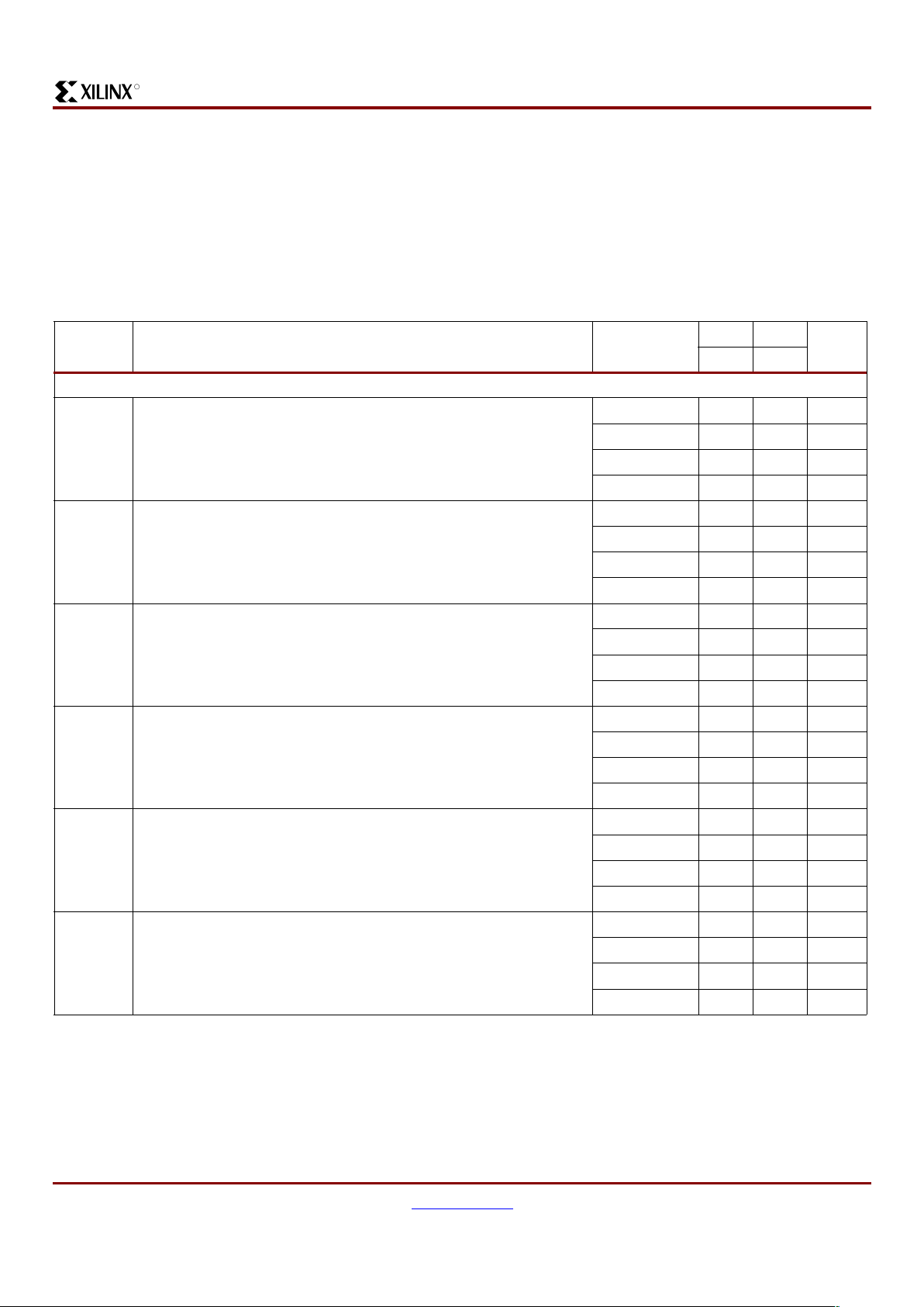
XQ4028EX CLB Level-Sensitive RAM Timing Waveforms
Figure 1:
DS021_03_060100
WE
ADDRESS
WRITE
READ WITHOUT WRITE
READ, CLOCKING DATA INTO FLIP-FLOP
READ DURING WRITE, CLOCKING DATA INTO FLIP-FLOP
READ DURING WRITE
DATA IN
CLOCK
XQ,YQ OUTPUTS
WRITE ENABLE
DATA IN
(stable during WE)
WRITE ENABLE
DATA IN
CLOCK
DATA IN
(changing during WE)
X,Y OUTPUTS
VALID
VALID
OLD NEW
VALID
VALID (NEW)VALID (OLD)
VALID
T
AS
T
ILO
T
AH
T
DS
REQUIRED
T
DH
T
WP
T
WC
T
ICK
T
CH
T
CKO
X,Y OUTPUTS
X,Y OUTPUTS
XQ,YQ OUTPUTS
T
DH
T
WO
T
WO
T
DO
T
WCK
T
DCK
T
CKO
T
WP
T
WP
VALID
(OLD)
VALID
(PREVIOUS)
VALID
(NEW)

QPRO XQ4000E/EX QML High-Reliability FPGAs
DS021 (v2.2) June 25, 2000 www.xilinx.com 27
Product Specification 1-800-255-7778
R
XQ4028EX Pin-to-Pin Output Parameter Guidelines
Testing of switching parameters is modeled after testing
methods specified by MIL-M-38510/605. All devices are
100% functionally tested. Pin-to-pin timing parameters are
derived from measuring external and inter nal test patterns
and are guaranteed over worst-case operating conditions
(supply voltage and junction temperature). Listed below are
representative values for typical pin locations and nor mal
clock loading. For more specific, more precise, and
worst-case guaranteed data, reflecting the actual routing
structure, use the values provided by the static timing analyzer (TRCE in the Xilinx Development System) and
back-annotated to the simulation netlist. These path delays,
provided as a guideline, have been extracted from the static
timing analyzer report. Values apply to all XQ4000EX
devices unless otherwise noted.
XQ4028EX Output Flip-Flop, Clock to Out
(1,2)
XQ4028EX Output Mux, Clock to Out
(1,2)
XQ4028EX Output Level and Slew Rate Adjustments
The following table must be used to adjust output parameters and output switching characteristics.
Symbol
Description
-4
UnitsMax
T
ICKOF
Global low skew clock to output using OFF
(3)
16.6 ns
T
ICKEOF
Global early clock to output using OFF
(3)
13.1 ns
Notes:
1. Listed above are representative values where one global clock input drives one vertical clock line in each accessible column, and
where all accessible IOB and CLB flip-flops are clocked by the global cloc k net.
2. Output timing is measured at TTL threshold with 50 pF external capacitive load.
3. OFF = Output Flip-Flop
Symbol
Description
-4
UnitsMax
T
PFPF
Global low skew clock to TTL output (fast) using OMUX
3)
15.9 ns
T
PEFPF
Global early clock to TTL output (fast) using OMUXF
(3)
12.4 ns
Notes:
1. Listed above are representative values where one global clock input drives one vertical clock line in each accessible column, and
where all accessible IOB and CLB flip-flops are clocked by the global cloc k net.
2. Output timing is measured at ~50% V
CC
threshold with 50 pF external capacitive load. For di fferent loads, see graph below.
3. OMUX = Output MUX
Symbol Description
-4
UnitsMax
T
TTLOF
For TTL output FAST add 0 n s
T
TTLO
For TTL output SLOW add 2.9 ns
T
CMOSOF
For CMOS FAST output add 1.0 ns
T
CMOSO
For CMOS SLOW output add 3.6 ns

QPRO XQ4000E/EX QML High-Reliability FPGAs
28 www.xilinx.com DS021 (v2.2) June 25, 2000
1-800-255-7778 Product Specification
R
XQ4028EX Pin-to-Pin Input Parameter Guidelines
Testing of switching parameters is modeled after testing
methods specified by MIL-M-38510/605. All devices are
100% functionally tested. Pin-to-pin timing parameters are
derived from measuring external and inter nal test patterns
and are guaranteed over worst-case operating conditions
(supply voltage and junction temperature). Listed below are
representative values for typical pin locations and nor mal
clock loading. For more specific, more precise, and
worst-case guaranteed data, reflecting the actual routing
structure, use the values provided by the static timing analyzer (TRCE in the Xilinx Development System) and
back-annotated to the simulation netlist. These path delays,
provided as a guideline, have been extracted from the static
timing analyzer report. Values apply to all XQ4000EX
devices unless otherwise noted
XQ4028EX Global Low Skew Clock, Setup and Hold
XQ4028EX Global Early Clock, Setup and Hold for IFF
XQ4028EX Global Early Clock, Setup and Hold for FCL
XQ4028EX Input Threshold Adjustments
The following table must be used to adjust input parameters and input switching characteristics.
Symbol Description
-4
UnitsMin
T
PSD
Input setup time, using Global Low Skew clock and IFF (full delay) 8.0 ns
T
PHD
Input hold time, using Global Low Skew clock and IFF (full delay) 0 ns
Notes:
1. IFF = Flip-Flop or Latch
Symbol Description
-4
UnitsMin
(2)
T
PSEP
Input setup time, using Global Early clock and IFF (full delay) 6.5 ns
T
PHEP
Input hold time, using Global Early clock and IFF (full delay) 0 ns
Notes:
1. IFF = Flip-Flop or Latch
2. Setup parameters are for BUFGE #s 3, 4, 7 and 8. Add 1.6 ns for BUFGE #s 1, 2, 5 and 6.
Symbol Description
-4
UnitsMin
(2)
T
PFSEP
Input setup time, using Global Early clock and FCL (partial delay) 3.4 ns
T
PFHEP
Input hold time, using Global Early clock and FCL (partial delay) 0 ns
Notes:
1. FCL = Fast Capture Latch
2. For CMOS input levels, see the XQ4028EX Input Threshold Adjustments.
3. Setup time is measured with the f as test rout e and th e lightest load. Use the stat ic ti ming analy zer to determine the setup tim e under
given design conditions.
4. Hold time is measured using the f arthest di stance an d a ref er ence load of one cloc k pin per two IOBs . Use the stat ic tim ing analyzer
to determine the setup and hold tim es under given design conditions.
5. Setup parameters are for BUFGE #s 3, 4, 7 and 8. Add 1.2 ns for BUFGE #s 1, 2, 5 and 6.
Symbol Description
-4
UnitsMax
T
TTLI
For TTL input add 0 ns
T
CMOSI
For CMOS input add 0.3 ns

QPRO XQ4000E/EX QML High-Reliability FPGAs
DS021 (v2.2) June 25, 2000 www.xilinx.com 29
Product Specification 1-800-255-7778
R
XQ4028EX IOB Input Switching Characteristic Guidelines
Testing of switching parameters is modeled after testing
methods specified by MIL-M-38510/605. All devices are
100% functionally tested. Internal timing parameters are
derived from measuri ng i nter n al tes t patter ns. Listed below
are representative values. For more specific, more precise,
and worst-case guaranteed data, use t he values reported
by the static ti ming analyzer (TR CE in the Xilinx Develop-
ment System) an d back-ann otated to th e simu lation n etlist.
These path delays, provided as a guideline, have been
extracted from the static timing analyzer report. All timing
parameters assume worst-case operating conditions (supply voltage and junction tempe rature). Values apply to all
XQ4000EX devices unless otherwise noted.
Symbol Description
-4
UnitsMin
Clocks
T
OKIK
Delay from FCL enable (OK) active to IFF clock (IK) active edge 3.2 ns
Propagation Delays
T
PID
Pad to I1, I2 2.2 ns
T
PLI
Pad to I1, I2 via transparent input latch, no delay 3.8 ns
T
PPLI
Pad to I1, I2 via transparent input latch, partial delay 13.3 ns
T
PDLI
Pad to I1, I2 via transparent input latch, full delay 18. 2 ns
T
PFLI
Pad to I1, I2 via transparent FCL and input latch, no delay 5.3 ns
T
PPFLI
Pad to I1, I2 via transparent FCL and input latch, partial delay 13.6 ns
Propagation Delays (TTL Inputs)
T
IKRI
Clock (IK) to I1, I2 (flip-flop) 3.0 ns
T
IKLI
Clock (IK) to I1, I2 (latch enable, active Low) 3.2 ns
T
OKLI
FCL enable (OK) active edge to I1, I2 (via transparent standard input latch) 6.2 ns
Global Set/Reset
T
MRW
Minimum GSR pulse width 13.0 ns
T
RRI
Delay from GSR input to any Q 22.8 ns
Notes:
1. FCL = Fast Capture Latch, IFF = Input Flip-Flop or Latch
2. For CMOS input levels, see the "XQ4028EX Input Threshold Adjustments" on page 28.
3. For setup and hold times with respect to the clock inp ut pin, see the Global Low Sk ew Cloc k and Glob al Early Clock Setup and Hold
tables on page 28.

QPRO XQ4000E/EX QML High-Reliability FPGAs
30 www.xilinx.com DS021 (v2.2) June 25, 2000
1-800-255-7778 Product Specification
R
XQ4028EX IOB Input Switching Characteristic Guidelines (Continued)
Symbol
Description
-4
UnitsMin
Setup Times
T
PICK
Pad to Clock (IK), no delay 2.5 ns
T
PICKP
Pad to Clock (IK), partial delay 10.8 ns
T
PICKD
Pad to Clock (IK), full delay 15.7 ns
T
PICKF
Pad to Clock (IK), via transparent Fast Capture Latch, no delay 3.9 ns
T
PICKFP
Pad to Clock (IK), via transparent Fast Capture Latch, partial delay 12.3 ns
T
POCK
Pad to Fast Capture Latch Enable (OK), no delay 0.8 ns
T
POCKP
Pad to Fast Capture Latch Enable (OK), partial delay 9.1 ns
Setup Times (TTL or CMOS Inputs)
T
ECIK
Clock Enable (EC) to Clock (IK) 0.3 ns
Hold Times
T
IKPI
Pad to Clock (IK), no delay 0 ns
T
IKPIP
Pad to Clock (IK), partial delay 0 ns
T
IKPID
Pad to Clock (IK), full delay 0 ns
T
IKPIF
Pad to Clock (IK) via transparent Fast Capture Latch, no delay 0 ns
T
IKFPIP
Pad to Clock (IK) via transparent Fast Capture Latch, partial delay 0 ns
T
IKFPID
Pad to Clock (IK) via transparent Fast Capture Latch, full delay 0 ns
T
IKEC
Clock Enable (EC) to Clock (IK), no delay 0 ns
T
IKECP
Clock Enable (EC) to Clock (IK), partial delay 0 ns
T
IKECD
Clock Enable (EC) to Clock (IK), full delay 0 ns
T
OKPI
Pad to Fast Capture Latch Enable (OK), no delay 0 ns
T
OKPIP
Pad to Fast Capture Latch Enable (OK), partial delay 0 n s
Notes:
1. For CMOS input levels, see the "XQ4028EX Input Threshold Adjustments" on page28.
2. For setup and hold times wi th respe ct to th e cloc k input pin, see the Globa l Lo w Ske w Cloc k and Globa l Early Cloc k Setu p and Hold
tables on page 28.

QPRO XQ4000E/EX QML High-Reliability FPGAs
DS021 (v2.2) June 25, 2000 www.xilinx.com 31
Product Specification 1-800-255-7778
R
FXQ4028EX IOB Output Switching Characteristic Guidelines
Testing of switching parameters is modeled after testing
methods specified by MIL-M-38510/605. All devices are
100% functionally tested. Internal timing parameters are
derived from measuri ng i nter n al tes t patter ns. Listed below
are representative values. For more specific, more precise,
and worst-case guaranteed data, use t he values reported
by the static ti ming analyzer (TR CE in the Xilinx Develop-
ment System) an d back-ann otated to th e simu lation n etlist.
These path delays, provided as a guideline, have been
extracted from the static timing analyzer report. All timing
parameters assume worst-case operating conditions (supply voltage and junction temperature). For Propagation
Delays, slew-rate = fast unless otherwise noted. Values
apply to all XQ4000EX devices unless otherwise noted.
Symbol Description
-4
UnitsMin Max
Propagation Delays (TTL Output Levels)
T
OKPOF
Clock (OK) to pad, fast - 7.4 ns
T
OPF
Output (O) to pad, fast - 6.2 ns
T
TSHZ
3-state to pad High-Z, slew-rate independent - 4.9 ns
T
TSONF
3-state to pad active and valid, fast - 6.2 ns
T
OKFPF
Output MUX select (OK) to pad - 6.7 ns
T
CEFPF
Fast path output MUX input (EC) to pad - 6.2
T
OFPF
Slowest path output MUX input (EC) to pad - 7.3
Setup and Hold Times
T
OOK
Output (O) to clock (OK) setup time 0.6 - ns
T
OKO
Output (O) to clock (OK) hold time 0 - ns
T
ECOK
Clock enable (EC) to clock (OK) setup 0 - ns
T
OKEC
Clock enable (EC) to clock (OK) hold 0 - ns
Clocks
T
CH
Clock High 3.5 - ns
T
CL
Clock Low 3.5 - ns
Global Set/Reset
T
MRW
Minimum GSR pulse width 13.0 - ns
T
RRI
Delay from GSR input to any pad 30.2 - ns
Notes:
1. Output timing is measured at TTL threshold, with 35 pF external capacitive loads.
2. For CMOS output levels, see the "XQ4028EX Output Level and Slew Rate Adjustments" on page 27.

QPRO XQ4000E/EX QML High-Reliability FPGAs
32 www.xilinx.com DS021 (v2.2) June 25, 2000
1-800-255-7778 Product Specification
R
CB191/196 Package for XQ4010E
Pin Description PG191 CB196
Bound
Scan
GND D4 P1 -
PGCK1_(A16*I/0) C3 P2 122
I/O_(A17) C4 P3 125
I/0 B 3 P4 128
--P5
(1)
-
I/O C5 P6 131
I/O_(TDI) A2 P7 134
I/O_(TCK) B4 P8 137
I/O C6 P9 140
I/O A3 P10 143
I/O B5 P11 146
I/O B6 P12 149
GND C7 P13 -
I/O A4 P14 152
I/O A5 P15 155
I/O_(TMS) B 7 P16 158
I/O A6 P17 161
I/O C8 P18 164
I/O A7 P19 167
I/O B8 P20 170
I/O A8 P21 173
I/O B9 P22 176
I/O C9 P23 179
GND D9 P24 VCC D10 P25 -
I/O C10 P26 182
I/O B10 P27 185
I/O A9 P28 -
I/O A10 P29 191
I/O A11 P30 194
I/O C11 P31 197
I/O B11 P32 200
I/O A12 P33 203
Notes:
1. Indicates unconnected package pins.
2. Contributes only one bit (.I) to the boundary scan register.
Boundary Scan Bit 0 = TD0.T
Boundary Scan Bit 1 = TD0.0
Boundary Scan Bit 487 = BSCAN.UPD
I/O B12 P34 206
I/O A13 P35 209
GND C12 P36 -
I/O B13 P37 212
I/O A14 P38 215
I/O A15 P39 218
I/O C13 P40 221
I/O B14 P41 224
I/O A16 P42 227
I/O B15 P43 230
I/O C14 P44 233
I/O A17 P45 236
SCGK2_(I/O) B16 P46 239
M1 C15 P47 242
GND D15 P48 -
M0 A18 P49 245
(2)
VCC D16 P50 -
M2 C16 P51 246
(2)
PGCK2_(I/O) B17 P52 247
I/O_(HDC) E16 P53 250
--P54
(1)
-
I/O C17 P55 253
I/0 D17 P56 256
I/O B18 P57 259
I/O_(LDC) E17 P58 262
I/O F16 P59 265
I/O C18 P60 268
I/O D18 P61 271
I/O F17 P62 274
GND G16 P63 -
I/O E18 P64 277
I/O F18 P65 280
I/O G17 P66 283
I/O G18 P67 286
Pin Description PG191 CB196
Bound
Scan
Notes:
1. Indicates unconnected package pins .
2. Contributes only one bi t (. I) to the boundary scan register.
Boundary Scan Bit 0 = TD0.T
Boundary Scan Bit 1 = TD0.0
Boundary Scan Bit 487 = BSCAN.UPD

QPRO XQ4000E/EX QML High-Reliability FPGAs
DS021 (v2.2) June 25, 2000 www.xilinx.com 33
Product Specification 1-800-255-7778
R
I/O H16 P68 286
I/O H17 P69 291
I/O H18 P70 295
I/O J18 P71 298
I/O J17 P72 301
I/O_(/ERR_/INIT) J16 P73 304
VCC J15 P74 GND K15 P75 -
I/O K16 P76 307
I/O K17 P77 310
I/O K18 P78 313
I/O L18 P79 316
I/O L17 P80 319
I/O L16 P81 322
I/O M18 P82 325
I/O M17 P83 328
I/O N18 P84 331
I/O P18 P85 334
GND M16 P86 -
I/O N17 P87 337
I/O R18 P88 340
I/O T18 P89 343
I/O P17 P90 349
I/O N16 P91 349
I/O T17 P92 352
I/O R17 P93 355
I/O P16 P94 358
I/O U18 P95 361
SGCK3_(I/O) T16 P96 364
GND R16 P97 -
DONE U17 P98 -
VCC R15 P99 -
/PROG V18 P100 -
I/O_(D7) T15 P101 367
Pin Description PG191 CB196
Bound
Scan
Notes:
1. Indicates unconnected package pins.
2. Contributes only one bit (.I) to the boundary scan register.
Boundary Scan Bit 0 = TD0.T
Boundary Scan Bit 1 = TD0.0
Boundary Scan Bit 487 = BSCAN.UPD
PGCK3_(I/O) U16 P102 370
--P103
(1)
I/O T14 P104 376
I/O U15 P105 376
I/O_(D6) V17 P106 379
I/O V16 P107 382
I/O T13 P108 385
I/O U14 P109 388
I/O V15 P110 391
I/O V14 P111 394
GND T12 P112 -
I/O U13 P113 397
I/O V13 P114 400
I/O_(D5) U12 P115 403
I/O_(/CSO) V12 P116 406
I/O T11 P117 409
I/O U11 P118 412
I/O V11 P119 415
I/O V1 P120 418
I/O_(D4) U10 P121 421
I/O T10 P122 424
VCC R10 P123 GND R9 P124 -
I/O_(D3) T9 P125 427
I/O_(/RS) U9 P126 430
I/O V9 P127 433
I/O V8 P128 436
I/O U8 P129 439
I/O T8 P130 442
I/O_(D2) V7 P131 445
I/O U7 P132 448
I/O V6 P133 451
I/O U6 P134 454
GND T7 P135 -
Pin Description PG191 CB196
Bound
Scan
Notes:
1. Indicates unconnected package pins .
2. Contributes only one bi t (. I) to the boundary scan register.
Boundary Scan Bit 0 = TD0.T
Boundary Scan Bit 1 = TD0.0
Boundary Scan Bit 487 = BSCAN.UPD

QPRO XQ4000E/EX QML High-Reliability FPGAs
34 www.xilinx.com DS021 (v2.2) June 25, 2000
1-800-255-7778 Product Specification
R
Additional XQ4010E Package Pins
I/O V5 P136 457
I/O V4 P137 460
I/O U5 P138 463
I/O T6 T139 446
I/O_(D1) V3 P140 469
I/O_(RCLK-/BUSY/RDY) V2 P141 472
I/O U4 P142 475
I/O T5 P143 478
I/O_(D0*_DIN) U3 P144 481
SGCK4_(DOUT*_I/O) T4 P145 484
CCLK V1 P146 -
VCC R4 P14 7 TDO U2 P148 GND R3 P149 -
I/O_(A0*_WS) T3 P150 2
PGCK4_(I/O*_A1) U1 P151 5
- - P152
(1)
I/O P3 P153 8
I/O R2 P154 11
I/O_(CS1*_A2) T2 P155 14
I/O_(A3) N3 P156 17
I/O P2 P157 20
I/O T1 P158 23
I/O R1 P159 26
I/O N2 P160 29
GND M3 P161 -
I/O P1 P162 32
I/O N1 P163 35
I/O_(A4) M 2 P164 38
I/O_(A5) M 1 P165 41
I/O L3 P166 44
I/O L2 P167 47
I/O L1 P168 50
Pin Description PG191 CB196
Bound
Scan
Notes:
1. Indicates unconnected package pins.
2. Contributes only one bit (.I) to the boundary scan register.
Boundary Scan Bit 0 = TD0.T
Boundary Scan Bit 1 = TD0.0
Boundary Scan Bit 487 = BSCAN.UPD
I/O K1 P169 53
I/O_(A6) K2 P170 56
I/O_(A7) K3 P171 59
GND K4 P172 -
VCC J4 P173 I/O_(A8) J3 P174 62
I/O_(A9) J2 P175 65
I/O J1 P176 68
I/O H1 P177 71
I/O H2 P178 74
I/O H3 P179 77
I/O_(A10) G1 P180 80
I/O_(A11) G2 P181 83
I/O F1 P182 86
I/O E1 P183 89
GND G3 P184 -
I/O F2 P185 92
I/O D1 P186 96
I/O C1 P187 98
I/O E2 P188 101
I/O_(A12) F3 P189 104
I/O_(A13 D2 P 190 107
--P192
(1)
-
I/O E3 P193 113
I/O_(A14) C2 P194 116
SGCK1(A15*I/O) B2 P195 119
VCC D3 P196 -
CB196
No Connect Pins
P5 P54 P103 P152
P192 - - -
Pin Description PG191 CB196
Bound
Scan
Notes:
1. Indicates unconnected package pins .
2. Contributes only one bi t (. I) to the boundary scan register.
Boundary Scan Bit 0 = TD0.T
Boundary Scan Bit 1 = TD0.0
Boundary Scan Bit 487 = BSCAN.UPD

QPRO XQ4000E/EX QML High-Reliability FPGAs
DS021 (v2.2) June 25, 2000 www.xilinx.com 35
Product Specification 1-800-255-7778
R
Revision History
The following table shows the revision history for this document
Date Version Descri ption
05/19/98 2.1 Updates.
06/25/00 2.2 Updated timing specifications to match with commercial data sheet. Updated format .
XQ4005E
XQ4010E
XQ4013E
XQ4025E
XQ4028EX
XQ 4010E -4 PG 191 M
Device Type
Speed Grade
Package Type
Number of Pins
Temp erature Range
Ordering Information
M = Cera mic (TC = –55°C to +125°C)
N = Plastic (T
J
= –55°C to +125°C)
CB = Top Brazed Ceramic Quad Flat Pack
PG = Ceramic Pin Grid Array
HQ = Plastic Quad Flat Pack
BG = Plastic Ball Grid Array
-3
-4
MIL-PRF-38535
(QML) Processing

QPRO XQ4000E/EX QML High-Reliability FPGAs
36 www.xilinx.com DS021 (v2.2) June 25, 2000
1-800-255-7778 Product Specification
R
 Loading...