

XILINX XCS40-4PQ240C, XCS40-4PQ208C, XCS40-4BG256C, XCS40-3PQ240C, XCS40-3PQ208I Datasheet
...
DS060 (v1.6) September 19, 2001 www.xilinx.com 1
Product Specification 1-800-255-7778
© 2001 Xilinx, Inc. All rights reserved. All Xilinx trademarks, registered trademarks, patents, and disclaimers are as listed at http://www.xilinx.com/legal.htm.
All other trademarks and registered trademarks are the property of their respective owners. All specifications are subject to change without notice.
Introduction
The Spar tan™ and the Spar tan-XL families are a high-volume production FPGA solution that delivers all the key
requirements for ASIC replacement up to 40,000 gates.
These requirements include high performance, on-chip
RAM, core solutions and prices that, in high volume,
approach and in many cases are equi valent to mask programmed ASIC devices.
The Spartan serie s is the result of more than 14 years of
FPGA design experience and feedback from thousands of
customers. By streamlining the Spar tan series feature set,
leveraging advanced process technologies and focusing on
total cost management, the S partan serie s delivers the key
features required by ASIC and other high-volume logic
users while avoiding the initial cost, long development
cycles and inherent r isk of c onventional ASICs. The Spartan and Spartan-XL families in the S partan series have ten
members, as shown in Table 1.
Spartan and Spartan-XL Features
Note: The Spartan series devices described in this data
sheet include the 5V Spartan family and the 3.3V
Spartan-XL family . See the separate data sheet for the 2.5V
Spartan-II family.
• First ASIC replacement FPGA for high-volume
production with on-chip RAM
• Density up to 1862 logic cells or 40,000 system gates
• Streamlined feature set based on XC4000 architecture
• System performance beyond 80 MHz
• Broad set of AllianceCOR E ™ and LogiCORE™
predefined solutions available
• Unlimited reprogrammability
• Low cost
• System level features
- Available in both 5V and 3.3V versions
- On-c h ip SelectRAM™ memory
- Fully PCI comp lia nt
- Full readback capability for program verification
and internal node obser vability
- Dedicated high-speed carry logic
- Internal 3-state bus capability
- Eight global low-skew clock or signal networks
- IEEE 1149.1-compatible Boundary Scan logic
- Low cost plastic packages available in all densities
- Footprint compatibility in common packages
• Fully supported by powerful Xilinx development system
- Foundation Series: Integrated, shrink-wrap
software
- Alliance Series: Dozens of PC and workstation
third party development systems supported
- Fully automatic mapping, placement and routing
Additional Spartan-XL Features
• 3.3V supply for low power with 5V tolerant I/Os
• Power down input
• Higher performance
• Faster carry logic
• More flexible high-speed clock network
• Latch capability in Configurable Logic Blocks
• Input fast capture latch
• Optional mux or 2-input function generator on outputs
• 12 mA or 24 mA output drive
• 5V and 3.3V PCI compliant
• Enhanced Boundary Scan
• Express Mode configuration
• Chip scale packaging
0
Spartan and Spartan-XL Families
Field Programmable Gate Arrays
DS060 (v1.6) September 19, 2001
00
Produc t S pecification
R
Table 1: Spartan and Sparta n- X L Fi el d Programmable Gat e A rray s
Device
Logic
Cells
Max
System
Gates
Typical
Gate Range
(Logic and RAM)
(1)
CLB
Matrix
Total
CLBs
No. of
Flip-flops
Max.
Avail.
User I/O
Total
Distributed
RAM Bits
XCS05 and XCS05XL 238 5,000 2,000-5,000 10 x 10 100 360 77 3,200
XCS10 and XCS10XL 466 10,000 3,000-10,000 14 x 14 196 616 112 6,272
XCS20 and XCS20XL 950 20,000 7,000-20,000 20 x 20 400 1,120 160 12,800
XCS30 and XCS30XL 1368 30,000 10,000-30,000 24 x 24 576 1,536 192 18,432
XCS40 and XCS40XL 1862 40,000 13,000-40,000 28 x 28 784 2,016 224 25,088
Notes:
1. Max values of Typical Gate Range i nclude 20-30% of CLBs used as RAM.
Spartan and Spartan -XL Families Field Programm able Gate Arrays
2 www.xilinx.com DS060 (v1.6) September 19, 2001
1-800-255-7778 Product Speci fication
R
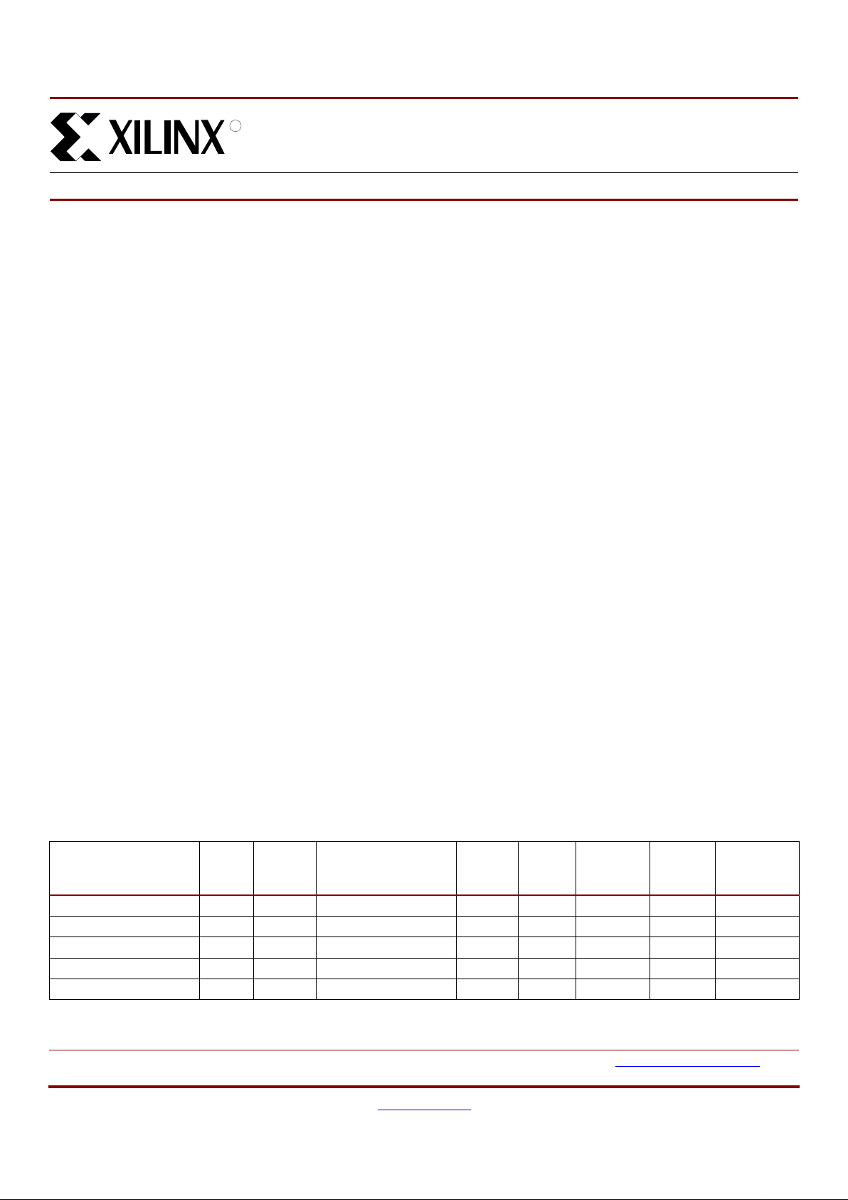
General Overview
Spartan series FPGAs are implemented with a regular, flexible, programmable architecture of Configurable Logic
Blocks (CLBs), interconnected by a powerful hierarchy of
versatile routing resources (routing channels), and surrounded by a perimeter of programmable Input/Output
Blocks (IOBs), as seen in Figure 1. They have generous
routing resources to accommoda te the mos t co mplex interconnect patterns.
The devices are customized by loading configuration data
into internal static m em ory cells. Re-programming is po ssible an unlimited number of times. The values stored in these
memory cells determine the logic functions and interconnections implemented in the FPGA. The FPGA can either
actively read its configuration data from an external seria l
PROM (Master Serial mode), or the configuration data can
be written into the FPGA from an external device (Slave
Serial mode).
Spart an series FPGAs can be used where hardware must
be adapted to different user applications. FPGA s are ideal
for shortening design and development cycles, and also
offer a cost-effective solution for production rates well
beyond 50,000 systems per month.
Figure 1: Basic FPGA Block Diagram
CLB
B-
SCAN
CLB CLB CLB
CLB CLB
Routing Channels
VersaRing Routing Channels
CLB CLB
CLB CLB CLB CLB
CLB CLB CLB CLB
IOB
IOB
IOB
IOB
IOB
IOB
IOB
IOB
IOB
IOB
IOB
IOB
IOB
IOB
IOB
IOB
IOB
IOB
IOB
IOB
IOB
IOB
IOB
IOB
IOB
IOB
IOB
IOB
IOB
IOB
IOB
IOB
RDBK
START
-UP
OSC
DS060_01_081100

Spartan and Spartan -XL Families Field Programmabl e Gate Arrays
DS060 (v1.6) September 19, 2001 www.xilinx.com 3
Product Speci fication 1-800-255-7778
R
Spartan series devices achieve high-performance, low-cost
operation through the use of an advanced architecture and
semiconductor technology. Spartan and Spartan-XL
devices provide system clock rates exceeding 80 MHz and
internal performance in excess of 150 MHz. In contrast to
other FPGA devices, the Spartan series offers the most
cost-effective solution while maintaining lead ing-edge performance. In addition to the conventional benefit of high volume programmable logic solutions, Spar tan series F PGAs
also offer on-chip edge-triggered single-port and du al-port
RAM, clock enables on all flip-flops, fast carry logic, and
many other features.
The Spartan/XL families leverage the highly successful
XC4000 architecture with many of that family’s features and
benefits. Technology advancements have been derived
from the XC4000XLA process developments.
Logic Functional Description
The Spartan series uses a standard FPGA structure as
shown in Figure 1, page 2. The FPGA consists of an array
of configurable logic blocks (CLBs) placed in a matrix of
routing channels. The input and output of signals is
achieved through a set of input/output b locks (IOBs) f orming
a ring around the CLBs and routing channels.
• CLBs provide the functional elements for implementing
the user’s logic.
• IOBs provide the interface between the package pins
and internal signal lines.
• Routing channels provide paths to interconnect the
inputs and outputs of the CLBs and IOBs.
The functionality of each circuit block is customized during
configuration by programming internal static memory cells.
The values stored in these memory cells determine the
logic functions and interconnections implemented in the
FPGA.
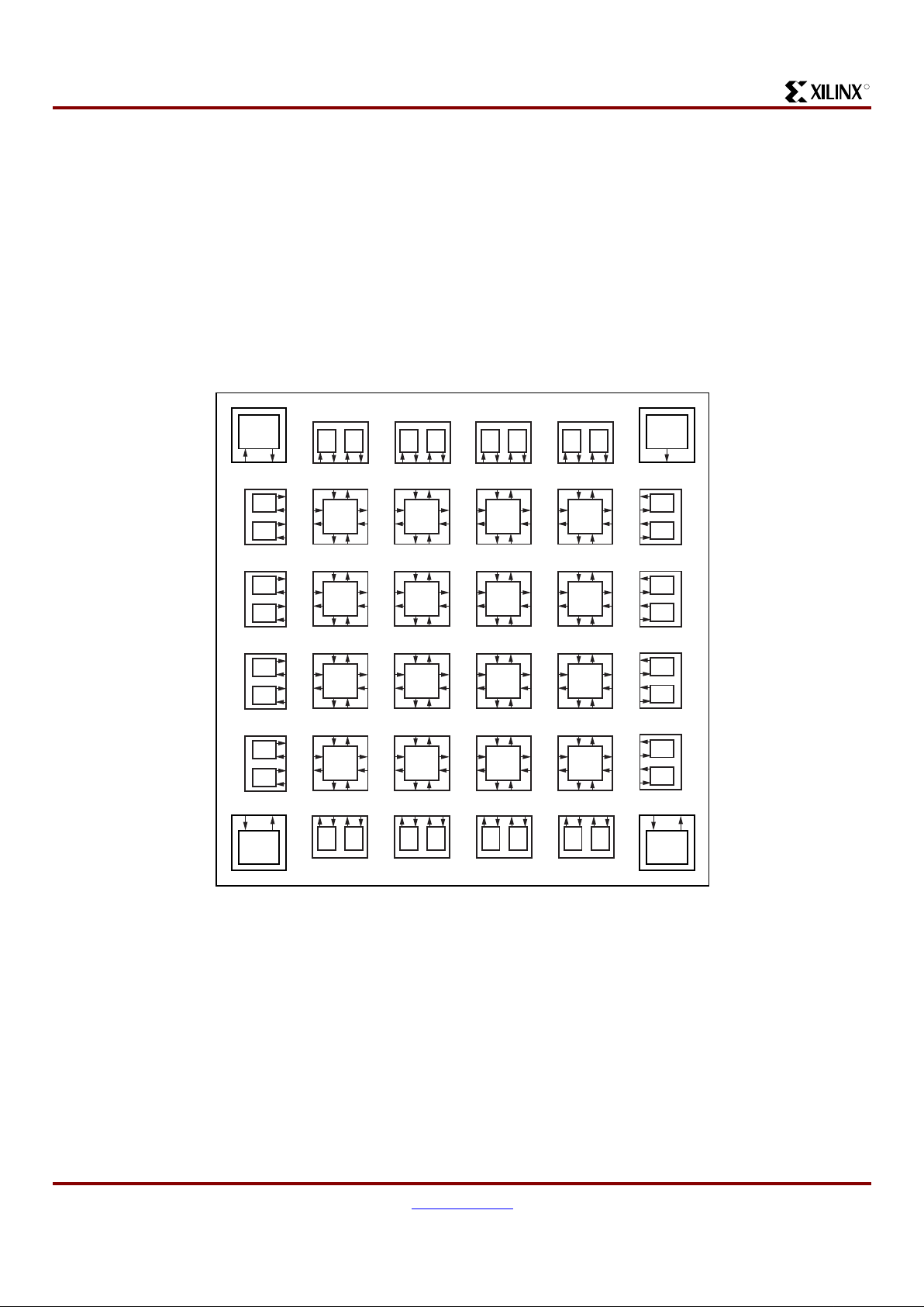
Configurable Logic Blocks (CLBs)
The CLBs are used t o implement most of the logic in an
FPGA. The principal CLB elements are shown in the simplified block diagram in Figure 2. There are three look-up
tables (LUT) which are used as logic funct ion generators,
two flip-flops and two groups of signal steering multiplexers.
There are also so me more advanced features provided by
the CLB which will be covered in the Advanced Features
Description, page 13.
Function Generators
Two 16 x 1 mem ory look-up t ables (F-LUT and G-LUT) are
used to impleme nt 4-input function gene rators, each offering unrestricted logic im plementation of any Bool ean function of up to four independent i nput s ignals (F1 to F4 or G1
to G4). Using memory look-up tables the propagation delay
is independent of the function implemented.
A third 3-input function generator (H-LUT) can implement
any Boolean function of its three inputs. Two of these inputs
are controlled by programmable multiplexers (see bo x "A" of
Figure 2). These inputs can come from the F-LUT or G-LUT
outputs or from CLB inpu ts. The third input always comes
from a CLB input. The CLB c an, therefore, implement certain functions of up to nine inputs, like parity checking. The
three LUTs in the CLB can also be combined to do any arbitrarily defined Boolean function of five inputs.
Spartan and Spartan -XL Families Field Programm able Gate Arrays
4 www.xilinx.com DS060 (v1.6) September 19, 2001
1-800-255-7778 Product Speci fication
R
A CLB can implement any of the following functions:
• Any function of up to four variables, plus any second
function of up to four unrelated variables, plus any third
function of up to three unrelated variables
Note: When three separate functions are generated, one of
the function outputs must be captured in a flip-flop internal to
the CLB. Only two unregistered functi on generator outputs
are available from the CLB .
• Any single function of five variables
• Any function of four variables together with some
functions of six variables
• Some functions of up to nine variables.
Implementing wide functions in a s ingle block reduces both
the number of blocks required and the delay in the signal
path, achieving both increased capacity and speed.
The versatility of the CLB function generat ors significantly
improves system speed. In addition, the design-software
tools can deal with each fun ction generator independently.
This flexibility improves cell usage.
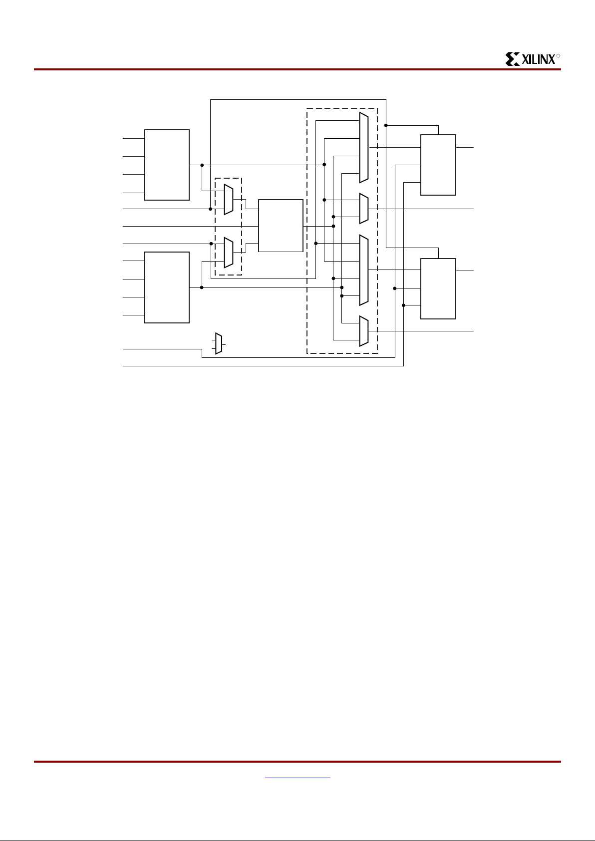
Flip-Flops
Each CLB contains two flip-flops that can be used to register (store) the function generator outputs. The flip-flops and
function generators can a lso be used independently (see
Figure 2). The CLB input DIN can be used as a direct input
to either of the two flip-flops. H1 can also drive either
flip-flop via the H-LUT with a slight additional delay.
The two flip-flops have common clock (CK), clock enable
(EC) and set/reset (SR) inputs. Inter nally both f lip-flops are
also controlled by a global initialization signal (GSR) wh ich
is described in detail in Global Signals: GSR and GTS,
page 20.
Latches (Spartan-XL only)
The Spartan-X L CLB storage elements can also be configured as latches. The two latches have common clock (K)
and clock enable (EC) inputs. Functionality of the storage
element is described in Table 2.
Figure 2: Spartan/XL Simplified CLB Logic Diagram (some features not shown)
G4
G
H1
F
G4
G3
G3
G2
G2
G1
DYQ
Y
X
SR
CK
EC
Q
G1
SR
H1
DIN
G
H
Logic
Function
of
G1-G4
Logic
Function
of
F-G-H1
Multiplexer Controlled
by Configuration Program
G-LUT
F4
F4
F3
F3
F2
F2
F1
F1
K
EC
G
Logic
Function
of
F1-F4
F-LUT
H-LUT
A
B
DXQ
SR
CK
EC
Q
DS060_02_0506 01
Spartan and Spartan -XL Families Field Programmabl e Gate Arrays
DS060 (v1.6) September 19, 2001 www.xilinx.com 5
Product Speci fication 1-800-255-7778
R
.
Clock Input
Each flip-flop can be triggered on either the rising or falling
clock edge. The CLB clock line is shared by both flip-flops.
However, the clock is individually invertible for each flip-flop
(see CK path in Figure 3). Any inverter placed on the clock
line in the design is automatically absorbed into the CLB.
Clock Enable
The clock enable line (EC) is active High. The EC line is
shared by both flip-flops in a CLB. If either one is left disconnected, the clock enable for that flip-flop defaults to the
active state. EC is not inver tible within the CLB. The clock
enable is synchronous to the clock and must satisfy the
setup and hold timing specified for the device.
Set/Reset
The set/reset line (SR) is an asynchronous active High control of the flip-flop. SR can be configured as either set or
reset at each flip-flop. This configuration option determines
the state in which each flip-flop becomes operational after
configuration. It also determines t he effect of a GSR pulse
during normal operation, and the effect of a pulse on the SR
line of the CLB. The S R line is sha red by both flip-flops. If
SR is not specified for a flip-flop the set/reset f or th at flip-flop
defaults to the inactive state. SR is not invertible within the
CLB.
CLB Signal Flow Control
In addition to the H-LUT input control multiplexers (s hown in
box "A" of Figure 2, page 4) there are signal flow control
multiplexers (shown in box "B" of Figure 2) which selec t th e
signals which drive the flip-flop inputs and the combinatorial
CLB outputs (X and Y).
Each flip-flo p input is driven from a 4:1 mult iplexer which
selects among the three LUT outputs and DIN as the data
source.
Each combinatoria l output is driven from a 2:1 m ultiplexer
which selects between two of the LUT outputs. The X output
can be driven from the F-LUT or H-LUT, the Y output from
G-LUT or H-LUT.
Control Signals
There are four signal control multiplex ers on t he input of the
CLB. These multiplexers allow the internal CLB control signals (H1, DIN, SR, and EC in Figure 2 and Figure 4) to b e
driven from any of the four general control inputs (C1-C4 in
Figure 4) into the CLB. Any of these inputs can drive any of
the four internal control signals.
Table 2: CLB St orage Element Functionality
Mode CK EC SR D Q
Power-Up or
GSR
XXXXSR
Flip-Flop
Operation
XX1XSR
1* 0* D D
0X0*XQ
Latch
Operation
(Spartan-XL)
11*0*XQ
01*0*DD
Both X 0 0* X Q
Legend:
XDon’t care
Rising edge (clock not inverted).
SR Set or Reset value. Reset is default.
0* Input is Low or unconnected (default
value)
1* Input is High or unconnected (default
value)
Figure 3: CLB Flip-Flop Functional Block Diagram
Multiplexer Controlled
by Configuration Program
DQQD
GND
GSR
Vcc
CK
EC
SR
SD
RD
DS060_03_041901
Spartan and Spartan -XL Families Field Programm able Gate Arrays
6 www.xilinx.com DS060 (v1.6) September 19, 2001
1-800-255-7778 Product Speci fication
R
The four internal control signals are:
• EC: Enable Clock
• SR: Asynchronous Set/Reset or H function generator
Input 0
• DIN: Direct In or H function generator Input 2
• H1: H function generator Input 1.
Input/Output Bloc ks (IOBs)
User-configurable input/output blocks (IOBs) provide the
interface between external package pins and the internal
logic. Each IOB controls o ne package pin and c an be configured for input, output, or bidirectional signals. Figure 6
shows a simplified functional block diagram of the Spartan/X L IOB.
IOB Input Signal Pa th
The input signal to the IOB can be configured to either go
directly to the routing channels (via I1 and I2 in Figure 6) or
to the input register. The input register can be programmed
as either an edge-triggered flip-flop or a level-sensitive
latch. The functionality of this register is shown in Table 3,
and a simplified block diagram of the register can be seen in
Figure 5.
Figure 4: CLB Control Signal Interface
Multiplexer Controlled
by Configuration Program
C1
DIN
H1
SR
EC
C2
C3
C4
DS060_04_081100
Figure 5: IOB Flip-Flo p/ La t ch Function al Bl ock
Diagram
Table 3: Input Register Functionality
Mode CK EC D Q
Power-Up or
GSR
XXXSR
Flip-Flop 1* D D
0XXQ
Latch 1 1* X Q
01*DD
Both X 0 X Q
Legend:
XDon’t care.
Rising edge (clock not inve rted).
SR Set or Reset value. Reset is default.
0* Input is Low or unconnected (default
value)
1* Input is High or unconnected (default
value)
Multiplexer Controlled
by Configuration Program
DQQD
GSR
Vcc
CK
EC
SD
RD
DS060_05_041901
Spartan and Spartan -XL Families Field Programmabl e Gate Arrays
DS060 (v1.6) September 19, 2001 www.xilinx.com 7
Product Speci fication 1-800-255-7778
R
The register choice is made by placing the appropriate
library symbol. For example, IFD is the basic input flip-flop
(rising edge triggered), and ILD is the basic input latch
(transparent-High). Va riations with inverted clocks are also
available. The clock signal inv erter is also shown in Figure 5
on the CK line.
The Spar tan IOB data input path has a one-tap delay element: either the delay is inserted (default), or it is not. The
Spartan-XL IOB data input path has a two-tap delay element, with choices of a full delay , a partial delay, or no delay .
The added delay guarantees a zero hold time with respect
to clocks routed through the global clock buffers. (See Glo-
bal Nets and Buffers, page 12 for a description of the glo-
bal clock buffers in the Spartan/XL families.) For a shorter
input register setup time, with positive hold-time, attach a
NODELA Y attrib ute or property to the flip-flop.The output of
the input register goes to the routing channels (via I1 and I2
in Figure 6). The I1 and I2 signals that exit the IOB can each
carry either the direct or registered input signal.
The 5V Spartan input buffers can be globally configured for
either TTL (1.2V) or CMOS (VCC/2) thresholds, using an
option in the bitstream generation software. The Spar tan
output levels are also configurable; the two global adjustments of input t hreshold and output l evel are independent.
The inputs of Spar t an devices can be driven by the outputs
of any 3.3V device, if the Spartan inputs are in TTL mode.
Input and output thresholds are TTL on all configuration
pins until the configuration has been loaded into the device
and specifies how they are to be used. Spar tan-XL inputs
are TTL compatible and 3.3V CMOS compatible.
Support ed sources for Spartan/X L device inputs are shown
in Table 4.
Spartan-XL I/Os are fully 5V tolerant even though the V
CC
is
3.3V. This allows 5V signals to directly connect to the Spartan-XL inputs without damage, as shown in Table 4. In addition, the 3.3V V
CC
can be applied before or after 5V signals
are applied to the I/Os. This makes the Sparta n-XL devices
immune to power supply sequencing problems.
Figure 6: Simplified Spartan/X L IOB Block Diagram
Multiplexer Controlled
by Configuration Program
T
O
OK
Q
GTS
D
CK
EC
I1
I2
IK
EC
QD
CK
EC
Delay
Package
Pad
Programmable
Pull-Up/
Pull-Down
Network
OUTPUT DRIVER
Programmable Slew Rate
Programmable TTL/CMOS Drive
(Spartan only)
INPUT BUFFER
DS060_06_041901
Spartan and Spartan -XL Families Field Programm able Gate Arrays
8 www.xilinx.com DS060 (v1.6) September 19, 2001
1-800-255-7778 Product Speci fication
R
Spartan-XL VCC Clamping
Spart an-XL FPGAs have an optional clamping diode connected from each I/O to V
CC
. When enabled they clamp
ringing transients back to the 3.3V supply rail. This clamping
action is required in 3.3V PCI applications. V
CC
clamping is
a global option affecting all I/O pins.
Spart an-XL devices are fully 5V TTL I/O compatible if V
CC
clamping is not ena bled. With VCC clamping enabled, the
Spartan-XL devices will begin to clamp input voltages to
one diode voltage drop above V
CC
. If enabled, TTL I/O compatibility is maintained but full 5V I/O tolerance is sacrificed.
The user may select either 5V tolerance (defaul t) or 3. 3V
PCI compatibility. In both cases negative voltage is clamped
to one diode voltage drop below ground.
Spart an-XL devices are compatible with TTL, LVTTL, PCI
3V, PCI 5V and LVCMOS signalling. The various standards
are illustrated in Table 5.
Additional Fast Ca p tu re In pu t La tch (Spartan- X L on ly)
The Spartan-XL IOB has an additional optional latch on the
input. This latch is clocked by the clock used for the output
flip-flop rather than the input clock. Therefore, two different
clocks can be used to clock the two input storage elements.
This additional latch allows the fast captu re of input data,
which is then synchronized to the internal clock by the IOB
flip-flop or latch.
To place the Fast Capture latch in a design, use one of the
special library symbols, ILFFX or ILFLX. IL FFX is a transparent-Low Fast Capture latch followed by an active High
input flip-flop. ILFLX is a transparent Low Fast Capture latch
followed by a transparent High input latch. Any of the clock
inputs can be inverted before driving the library element,
and the inverter is absorbed into the IOB.
IOB Output Signal Path
Output signals can be optionally inverted within the IOB,
and can pass directly to the output buffer or be stored in an
edge-triggered flip-flop and then to the output buffer. The
functionality of this flip-flop is shown in Table 6.
Table 4: Supported Sources for Spartan/XL Inputs
Source
Spartan
Inputs
Spartan-XL
Inputs
5V,
TTL
5V,
CMOS
3.3V
CMOS
Any de vice, VCC = 3.3V,
CMOS outputs
√ Unreli-
able
Data
√
Spartan family, VCC = 5V,
TTL outputs
√√
Any dev ice, VCC = 5V,
TTL outputs (V
OH
≤ 3.7V)
√√
Any dev ice, VCC = 5V,
CMOS outputs
√√√ (default
mode)
Table 5: I/O Standards Supported by Spartan-XL FPGAs
Signaling
Standard
VCC
Clamping
Output
Drive V
IH MAX
V
IH MIN
V
IL MAX
V
OH MIN
V
OL MAX
TTL Not allowed 12/24 mA 5.5 2.0 0.8 2.4 0.4
LVTTL OK 12/24 mA 3.6 2.0 0.8 2.4 0. 4
PCI5V Not allowed 24 mA 5.5 2.0 0.8 2. 4 0.4
PCI3V Required 12 mA 3.6 50% of V
CC
30% of V
CC
90% of V
CC
10% of V
CC
LVCM OS 3V OK 12/24 mA 3.6 50% of V
CC
30% of V
CC
90% of V
CC
10% of V
CC
Table 6: Output Fl ip - Fl op Functionality
Mode Clock
Clock
Enable T D Q
Power-Up
or GSR
XX0*XSR
Flip-Flop X 0 0* X Q
1* 0* D D
XX1XZ
0X0*XQ
Legend:
XDon’t car e
Rising edge (clock not inve rted).
SR Set or Reset value. Reset is defau lt.
0* Input is Low or unconnected (default value)
1* Inp ut is High or unconnected (default value)
Z 3-state
Spartan and Spartan -XL Families Field Programmabl e Gate Arrays
DS060 (v1.6) September 19, 2001 www.xilinx.com 9
Product Speci fication 1-800-255-7778
R
Output Multiplexer/2-Input Function Generator
(Spar tan-XL only)
The output path in the Spart an-XL IOB contains an additional multiplexer not available in the Spartan IOB. The multiplexer can also be configured as a 2-input function
generator, implementing a pass gate, AND gate, OR gate,
or XOR gate, with 0, 1, or 2 inverted inputs.
When configured as a mul tiplexer, this feature allows two
output signals to time-share the same output pad, effectively doubling the number of device outputs without requiring a larger, more expensive package. The select input is
the pin used for the output flip-flop clock, OK.
When the multiplexer is configured as a 2-input function
generator, logic can be implemented within the IOB itself.
Combined with a Global buffer, this arrangement allows
very high-speed gating of a single signal. For example, a
wide decoder can be i mplemented in CLBs, and its out put
gated with a Read or Write Strobe driven by a global buffer .
The user can specify that the IOB function generator be
used by placing special library s ymbols beginning with th e
letter "O." For example, a 2-input AND gate in the IOB function generator is called OAND2. Use the symbol input pin
labeled "F" for the signal on the critical path. This signal is
placed on the OK pin — the IOB input with the shortest
delay to the function generator. Two examples are shown in
Figure 7.
Output Buffer
An active High 3-state signal can be used to place the output buffer in a high-impedance state, implementing 3-state
outputs or bidirectional I/O. Under configuration control, the
output (O) and output 3-state (T) signals can be inverted.
The polarity of these signals is independently configured for
each IOB (see Figure 6, page 7 ). An output can be config-
ured as open-drain (open-collector) by tying the 3-state pin
(T) to the output signal, and the input pin (I) to Ground.
By default, a 5V Spartan device output buffer pull-up structure is configured as a TTL-like totem-pole. The High driver
is an n-channel pull-up tran sistor, pu lling to a voltage one
transistor threshold below V
CC
. Alternatively, the outputs
can be globally configured as CMOS drivers, with additional
p-channel pull-up transistors pulling to V
CC
. This option,
applied using the bits tream generation s oftware, applies to
all outputs on the device. It is not individually programmable.
All Spartan-XL device outputs are configured as CMOS
drivers, therefore driving rail-to-r ail. The Spartan-XL outputs
are individually programmable for 12 mA or 24 mA output
drive.
Any 5V Sparta n device with its outputs configured in TTL
mode can dr ive the inputs of any typical 3. 3V device. Supported destinations for Spartan/XL device outputs are
shown in Table 7.
Three-State Register (Spartan-XL Only)
Spartan-XL devices incorporate an optional register controlling the three-state enable in the IOBs. The use of the
three-state control register can significantly improve output
enable and disable time.
Output Slew Rat e
The slew rate of each out put buffer is, by default, reduced,
to minimize power bus transients when switching non-critical signals. For critical signals, attach a FAST attribute or
property to the output buffer or flip-flop.
Spartan/XL devices have a feature called "Soft Start-up,"
designed to reduce ground bounce when all outputs are
turned on simultaneously at the end of configuration.
When the configuration process is finished and the device
starts up, the first activation of the outputs is automatically
slew-rate limited. Immediately following the initial activation
of the I/O, the slew rate of the individual outputs is determined by the individual configuration option for each IOB.
Pull-up and Pull-down Network
Programmable pull-up and pull-down resistors are used for
tying unused pins to V
CC
or Ground to minimize power consumption and reduce noise sensitivity. The configurable
pull-up resistor is a p-channel transistor that pulls to V
CC
.
The configurable pull-down resistor is an n-channel transistor that pulls to Ground. The value of these resistors is typically 20 KΩ − 100 KΩ (See "Spartan DC Characteristics
Figure 7: AND and MUX Symbols in Spartan-XL IOB
DS060_07_081100
OAND2
OMUX2
F
D0
D1
O
S0
Spartan and Spartan -XL Families Field Programm able Gate Arrays
10 www.xilinx.com DS060 (v1.6) September 19, 2001
1-800-255-7778 Product Speci fication
R
Over Operating Conditions" on page 43.). This high value
makes them unsuitable as wired-AND pull-up resistors.
After configuration, voltage levels of unused pads, bonded
or unbonded, must be valid logic levels, to reduce noise
sensitivity and avoid excess current. Therefore, by default,
unused pads are configured with the internal pull-up resistor
active. Alternatively, they can be individually configured with
the pull-down resistor, or as a driven output, or to be driven
by an external source. T o activate the internal pull-up, attach
the PULLUP library com ponent to the net attached to the
pad. To activate the internal pull-down, attach the PULLDOWN library component to the net attached to the pad.
Set/Reset
As with the CLB registers, the GSR signal can be used to
set or clear the input and output registers, depending on the
value of the INIT attribute or property. The two flip-flops can
be individually configured to s et or c lear on reset and after
configuration. Other than the global GSR net, no user-controlled set/reset signal is available to the I/O flip-flops
(Figure 5). The choice of set or reset applies to both the initial state of the flip-flop and the response to the GSR pulse.
Independ ent C l ocks
Separate clock signals are provided for the input (IK) and
output (OK) flip-flops. The clock can be independently
inverted for each flip-flop within the IOB, generating either
falling-edge or rising-edge triggered flip-flops. The clock
inputs for each IOB are independent.
Common Clock Enables
The input and output flip-flops in eac h IOB have a common
clock enable input (see EC signal in Figure 5), which
through configuration, can be activated individually for the
input or output flip-flop, or both. This clock enable operates
exactly like the EC signal on the Spartan/XL CLB. It cannot
be inverted within the IOB.
Routing Ch annel Description
All internal rout ing channels are composed of metal segments with programmable switching points and switching
matrices to implement the desired routing. A structured,
hierarchical matrix of routing channels is provided to
achieve efficient automated routing.
This section describes the routing channels available in
Spartan/XL devices. Figure 8 shows a general block diagram of the CLB routing channels. The implementation software automatically assigns the appropriate resources
based on the density and timing requirements of the design.
The following description of the routing channels is for inf ormation only and is simplified with s ome minor details omitted. For an exact interconnect description the designer
should open a design in the FPGA E ditor and review the
actual connections in this tool.
The routing channels will be discussed as follows;
• CLB routing channels which run along each row and
column of the CLB array.
• IOB routing channels which form a ring (called a
VersaRing) around the outside of the CLB array. It
connects the I/O with the CLB routing channels.
• Global routing consists of dedicated networks primarily
designed to distribute clocks throughout the device with
minimum delay and skew. Global routing can also be
used for other high-fanout signals.
CLB Routing Channels
The routing channels around the CLB are derived from
three types of interconnects; single-length, double-length,
and longlines. At the intersection of each vertical and horizontal routing channel is a signal steering matrix ca lled a
Programmable Switch Matrix (PSM). Figure 8 shows the
basic routing channel configuration showing single-length
lines, double-length lines and longlines as well as the CLBs
and PSMs. The CLB to rout ing channel interface is shown
as well as how the PSMs interface at the channel intersections.
Table 7: Supported Destinations for Spartan/XL
Outputs
Destination
Spartan-XL
Outputs
Spartan
Outputs
3.3V, CMOS
5V,
TTL
5V,
CMOS
Any device,
V
CC
= 3.3V,
CMOS-threshold
inputs
√√Some
(1)
Any device,
V
CC
= 5V,
TTL-threshold inputs
√√√
Any device,
V
CC
= 5V,
CMOS-threshold
inputs
Unreliable
Data
√
Notes:
1. Only if destination device has 5V tolerant inputs.
Spartan and Spartan -XL Families Field Programmabl e Gate Arrays
DS060 (v1.6) September 19, 2001 www.xilinx.com 11
Product Speci fication 1-800-255-7778
R
CLB Interface
A block diagram of the CLB interface signals is shown in
Figure 9. The input signals to the CLB are distributed evenly
on all four sides providing maximum routing flexibility. In
general, the entire architecture is symmetrical and regular.
It is well suited to established placement and routing algorithms. Inputs, outputs, and function gene rators can freely
swap positions within a CLB to avoid routing congestion
during the placement and routing operation. The exceptions
are the clock (K) input and CIN/COUT signals. The K input
is routed to dedicate d global vertical lines as well as four
single-length lines and is on the left side of the CLB. The
CIN/COUT signals are routed through dedicated interconnects which do not interfere with the general routing structure. The output signals from the CLB
are available to drive
both vertical and horizontal channels.
Programmable Switch Matrices
The horizontal and vertical singl e- and double-length lines
intersect at a box called a programmable switch matrix
(PSM). Each PSM consists of programmable pass transistors used to establish connections between the lines (see
Figure 10).
For example, a single-length signal entering on the right
side of the switch matr ix can be routed to a single-length
line on the top, left, or bottom sides, or any combination
thereof, if multiple branches are required. Similarly, a double-length signal can be routed to a dou ble-length line on
any or all of the other three edges of the programmable
switch matrix.
Single-Length Li nes
Single-length lines provide the greatest interconnect flexibility and offer fast routing between adjacent blocks. There are
eight vertical and eight horizontal single-length lines associated with each CLB. These lines connect the switching
matrices that are located in every row and column of CLBs.
Single-length lines are connected by way of the programmable switch matrices, as shown in Figure 10. Routing connectivity is shown in Figure 8.
Single-length lines incur a delay whenever they go through
a PSM. Therefore, they are not suitable for routi ng signals
for long distances. They are normally used to conduct signals within a localized area and to provide the branching for
nets with fanout greater than one.
Figure 8: Spartan/XL CLB Routing Channels and Interface Block Diagram
PSM
CLB CLB
PSM PSM
PSM PSM PSM
8 Singles
2 Doubles
3 Longs
3 Longs
2 Doubles
2 Doubles
3 Longs3 Longs
2 Doubles
8 Singles
DS060_09_041901
Figure 9: CLB Interconnect Signals
CIN Y
G3
C3
F3
COUT
G1
C1
K
F1
X
XQ
F4
C4
G4
YQ
F2
C2
G2
CLB
DS060_08_081100
Rev 1.1
Spartan and Spartan -XL Families Field Programm able Gate Arrays
12 www.xilinx.com DS060 (v1.6) September 19, 2001
1-800-255-7778 Product Speci fication
R
Double-Le ng t h Li ne s
The double-length lines consist of a grid of metal segments,
each twice as long as the single-length lines: they run past
two CLBs before entering a PSM. Double-length lines are
grouped in pairs with the PSMs staggered, so that each line
goes through a P SM at every o ther row or c ol um n of CLBs
(see Figure 8).
There are four vertical and four horizontal double-length
lines associated with each CLB. T hese lines provide faster
signal routing over intermedi ate distances, while retaining
routing flexib ilit y.
Longlines
Longlines form a grid of metal intercon nect segments that
run the entire length or width of the array. Longlines are
intended for high fan-out, time-critical signal nets, or nets
that are distributed over long distances.
Each Spartan/XL device longline has a programmable splitter switch at its center. This s witch can separate the line into
two independent routing channels, each running half the
width or height of the array.
Routing connectivity of the longlines is shown in Figure 8.
The longlines also interface to some 3-state buffers which is
described later in 3-State Long Line Drivers, page 19.
I/O Routing
Spart an/XL d evices have additional routing around the I OB
ring. This routing is called a VersaRing. The VersaRing facilitates pin-swapping and redesign without affecting board
layout. Included are eight double-length lines, and four longlines.
Global Nets and Buffers
The Spartan/XL devices have dedicated global networks.
These networks are designed to distribute clocks and other
high fanout control signals throughout the devices with minimal skew.
Four vertical longlines in each CLB column are driven exclusively by special global buffers. These longlines are in addition to the vertical longlines used for standard interconnect.
In the 5V Spartan devices, the four global lines can be
driven by either of two types of global buffers; Primar y G lobal buffers (BUFGP) or Secondary Global buffers (BUFGS).
Each of these lines can be ac cessed by one par ticula r Primary Global buffer, or by any of the Seconda ry Global buffers, as shown in Figure 11. In the 3V Spar tan-XL devices,
the four global lines can be driven by any of the eight Global
Low-Skew Buffers (B UFGLS). The clock pins of every CLB
and IOB can also be sourced from local interconnect.
Figure 10: Programmable Switch Matrix
Six Pass Transistors Per
Switch Matrix Interconnect Point
DS060_10_081100
Spartan and Spartan -XL Families Field Programmabl e Gate Arrays
DS060 (v1.6) September 19, 2001 www.xilinx.com 13
Product Speci fication 1-800-255-7778
R
The four Primary Global buffers offer the shortest delay and
negligible skew. Four Secondary Global buffers have
slightly longer delay and slightly m ore skew due to potentially heavier loading, but offer greater flexibility when used
to drive non-clock CLB inputs. The eight Global Low-Skew
buffers in the Spartan-XL devices combine short delay, negligible skew, and flexibility.
The Primary Global buffers must be driven by the semi-dedicated pads (PGCK1-4). The Second ary Global buffers can
be sourced by either semi-dedicated pads (SGCK1-4) or
internal nets. Each cor ner of the devi ce has one Primar y
buffer and one Secondary buffer. The Spartan-XL family
has eight global low-skew buffers, two in each corn er. All
can be sourced by either semi-dedicated pads (GCK1-8) or
internal nets.
Using the library symbol called BUFG results in the software
choosing the appropria te clock buffer, based on t he timing
requirements of the design. A global buffer s ho uld be specified for all timing-sensitive global signal distribution. To use
a global buffer, place a BUFGP (primary buffer), BUFGS
(secondary buffer), BUFGLS (Spartan-XL global low-skew
buffer), or BUFG (an y buffer t ype) element in a schematic or
in HDL code.
Advanced Features Description
Distributed RAM
Optional modes for each CLB allow the function generators
(F-LUT and G-LUT) to be used as Random Access Memory
(RAM).
Read and write operations are significantly faster for this
on-chip RAM than for off-chip implem entations. T his speed
advantage is due to the relatively short signal propagation
delays within the FPGA.
Memory Configuration Overview
There are two available memory conf iguration modes: single-port RAM and dual-p ort RAM. For both these modes,
write operations are synchronous (edge-triggered), while
read operations are asynchronous. In the single-port mode,
a single CLB can be configured a s eit her a 16 x 1, (16 x 1)
x 2, or 32 x 1 RAM array. In the dual-por t mode, a single
CLB can be configured only as one 16 x 1 RAM array. The
different CLB memory configurations are summarized in
Table 8. Any of t hese possibilities ca n be individually pro-
grammed into a Spartan/XL CLB.
Figure 11: 5V Sparta n Family Gl obal Net Distribut io n
X4 X4
ds060_11_080400
X4
4
One BUFGP
per Global Line
One BUFGP
per Global Line
Any BUFGS Any BUFGS
BUFGP
PGCK4
SGCK4
PGCK3
SGCK3
BUFGS
BUFGP
BUFGS
IOB
IOB
IOBIOBIOBIOB
IOBIOBIOB
IOB
IOB
BUFGS
BUFGS
BUFGP
BUFGP
SGCK1
PGCK1
SGCK2
PGCK2
IOB
X4
locals
localslocals
locals
locals
locals
locals
locals
locals
locals
locals
locals
4
4
4
CLB
CLB
locals locals
CLB
CLB
locals
locals
Table 8: CLB Me m ory Configu r at i ons
Mode 16 x 1 (16 x 1) x 2 3 2 x 1
Single-Port √√√
Dual-Port √−−
Spartan and Spartan -XL Families Field Programm able Gate Arrays
14 www.xilinx.com DS060 (v1.6) September 19, 2001
1-800-255-7778 Product Speci fication
R
• The 16 x 1 single-port configuration contains a RAM
array with 16 locations, each one-bit wide. One 4-bit
address decoder determines the RAM location for write
and read operations. There is one input for writing data
and one output for reading data, all at the selected
address.
• The (16 x 1) x 2 single-port configuration combines two
16 x 1 single-port configurations (each according to the
preceding description). There is one data input, one
data output and one address decoder for each array.
These arrays can be addressed independently.
• The 32 x 1 single-port configuration contains a RAM
array with 32 locations, each one-bit wide. There is one
data input, one data output, and one 5-bit address
decoder.
• The dual-port mode 16 x 1 configuration contains a
RAM array with 16 locations, each one-bit wide. There
are two 4-bit address decoders, one for each port. One
port consists of an input for writing and an output for
reading, all at a selected address. The other port
consists of one output for reading from an
independently selected address.
The appropriate choice of RAM configuration mode for a
given design should be based on timing and resource
requirements, desired functionality, and the simplicity of the
design process. Selection criteria include the following:
Whereas the 32 x 1 single-port, the (16 x 1) x 2 single-port,
and the 16 x 1 dual-port configurations each use one entire
CLB, the 16 x 1 single-port configuration uses only one half
of a CLB. Due to its s imultane ous read/wr ite capa bility, the
dual-port RAM can transfer twice as much data as the single-port RAM, which permits only one data operation at any
given time.
CLB memory configuration options are selected by using
the appropriate library symbol in the design entry.
Single-Port Mode
There are three CLB memory configurations for the single-port RAM: 16 x 1, (16 x 1) x 2, and 32 x 1, the functional
organization of which is shown in F igure 12.
The single-port RAM signals and the CLB signals (Figure 2,
page 4) from which they are originally derived are shown in
Table 9.
Writing data to t he si ngle-port RAM is ess entially the s am e
as writing to a dat a register. It is an edge-triggered (synchronous) operation performed by applying an address to
the A inputs and data to the D input during the active edge
of WCLK while WE is High.
The timing relationship s are shown in Figure 13. The Hi gh
logic level on WE enables the input data register for writing.
The active edge of W CLK latches the ad dress, input data,
and WE signals. Then, an internal write pulse is generat ed
that loads the data into the memory cell.
Table 9: Single - Port R A M S ig nal s
RAM Signal Function CLB Signal
D0 or D1 Data In DIN or H1
A[3:0] Address F[4:1] or G[4:1]
A4 (32 x 1 only) Address H1
WE Write Enable SR
WCLK Clock K
SPO Single Port Out
(Data Out)
F
OUT
or G
OUT
Notes:
1. The (16 x 1) x 2 configurat ion com bines tw o 16 x 1 singl e-port
RAMs, each with its own independent address bus and data
input. The same WE and WCLK signa ls are connected to bot h
RAMs.
2. n = 4 for the 16 x 1 and (16 x 1) x 2 configurations. n = 5 for the
32 x 1 configuration.
Figure 12: Logic Diagr am for the Single-Port RA M
WE
WCLK
A[n-1:0]
D0 or D1
n
n
SPO
INPUT REGISTER
WRITE ROW
SELECT
WRITE
CONTROL
READ
OUT
16 x 1
32 x 1
RAM ARRAY
READ ROW
SELECT
DS060_12_043010
Spartan and Spartan -XL Families Field Programmabl e Gate Arrays
DS060 (v1.6) September 19, 2001 www.xilinx.com 15
Product Speci fication 1-800-255-7778
R
WCLK can be configured as active on either the rising edge
(default) or the falling edge. While the WCLK input to the
RAM accepts the same signal as the clock input to the associated CLB’s flip-flops, the sense of this WCLK input can be
inverted with respect to the sense of the flip-flop clock
inputs. Consequently, within the same CLB, data at the
RAMs SPO line can be st ored in a flip-flop with either the
same or the inverse clock polarity used to write data to the
RAM.
The WE input is active High and cannot be inverted within
the CLB.
Allowing for settling time, the data on the SPO output
reflects the contents of the RAM location currently
addressed. When the address changes, following the asynchronous delay T
ILO
, the data stored at the new address
location will appear on SPO. If the data at a particular RAM
address is overwritten, after the delay T
WOS
, the new data
will appear on SPO.
Dual-Port Mode
In dual-port mode, the function generators (F-LUT and
G-LUT) are used to create a 1 6 x 1 dual-port memor y. Of
the two data ports available, one permits read and write
operations at the address specified by A[3:0] while the second provides only for read operations at the address specified independently by DPRA[3:0]. As a result, simultaneous
read/write operations at different addresses (or even at the
same address) are suppor ted.
The functional organization of the 16 x 1 d ual-port RAM is
shown in Figure 14. The dual-port RAM signals and the
Figure 13: Data Write and Access Timing for RAM
DS060_13_080400
WCLK (K)
WE
ADDRESS
DATA IN
DATA OUT OLD NEW
T
DSS
T
DHS
T
ASS
T
AHS
T
WSS
T
WPS
T
WHS
T
WOS
T
ILO
T
ILO
Figure 14: Logic Diagram for the Dual-Port RAM
WE
WCLK
A[3:0]
D
44
4
4
SPO
DPRA[3:0]
INPUT REGISTER
WRITE ROW
SELECT
WRITE
CONTROL
READ
OUT
16 x 1
RAM
READ ROW
SELECT
DS060_14_043001
DPO
WRITE ROW
SELECT
WRITE
CONTROL
READ
OUT
16 x 1
RAM
READ ROW
SELECT
Spartan and Spartan -XL Families Field Programm able Gate Arrays
16 www.xilinx.com DS060 (v1.6) September 19, 2001
1-800-255-7778 Product Speci fication
R
CLB signals from which they are originally derived are
shown in Table 10.
The RAM16X1D primitive used to instantiate the dual-port
RAM consists of an upper and a lower 16 x 1 memory array .
The address port label ed A [3:0] supplies bot h the read and
write addresses for the lower memory array, which behaves
the same as the 16 x 1 single-port RAM array described
previously. Single Port Out (SPO) serves as the data output
for the lower me mory. Therefore, SPO reflects the data at
address A[3:0].
The other address por t, labeled DPRA[3:0] for Dual Port
Read Address, supplies the read address for the upper
memory. The write address for this memory, however,
comes from the address A[3:0]. Dual Port Out (DPO) serves
as the data output for the upper mem ory. Therefore, DPO
reflects the data at address DPRA[3:0].
By using A[3:0] for the write address and DPRA[3:0] for t he
read address, and reading only the DPO output, a FIFO that
can read and write simultane ously is easily generated. The
simultaneous read/write capability possible with the
dual-port RAM can provide twice the effective data throughput of a single-port RA M alternating read an d write operations.
The timing relationships for the dual-port RAM mode are
shown in Figure 13.
Note that write operations to RAM are synchronous
(edge-triggered); however, data access is asynchro nous.
Initializi ng R AM at FPGA Co nf i gu r at io n
Both RAM and ROM implementations in the Spartan/XL
families are initialized during device configuration. The initial
contents are defined via an INIT attribute or property
attached to the RAM or ROM symbol , as described in the
schematic library guide. If not defined, all RAM contents are
initialized to zeros, by default.
RAM initialization occurs only during device configu ration.
The RAM content is not affected by GSR.
More Information on Using RAM Inside CLBs
Three application notes are available from Xilinx that discuss synchronous (edge-triggered) RAM: "Xilinx Edge-Trig-
gered and Dual-Port RAM Capability," "Implementing FIFOs
in Xili n x R A M, " and "S yn chronous and Asynchronous FIFO
Designs." All three application notes apply to both the Spar-
tan and the Spartan-XL families.
Fast Carry Logic
Each CLB F-LUT and G-LUT contains dedicat ed ari thmet ic
logic for the fast generation of carry and borrow signals.
This extra output is passed on t o the function generator i n
the adjacent CLB. The carry chain is independent of normal
routing resources. (See Figure 15.)
Dedicated fast carry logic greatly increas es the efficiency
and performance of adders, subtractors, accumulators,
comparators and counters. It also opens the door to many
new applications involving arithmetic operation, where the
previous generations of FPGAs were not fast enough or too
inefficient. High-speed address offset calculat ions in microprocessor or graphics system s, and high-spe ed addition i n
digital signal processing are two typical applications.
The two 4-input function generators can be configured as a
2-bit adder with built-in hidden carry that can b e expanded
to any length. This dedi cated carry circuitr y is so fast and
efficient that conventional speed-up methods like carry generate/propagate are mean ingless even at the 16-bit level,
and of marginal benefit at the 32-bit level. This fast carry
logic is one of the more sign ificant features of the Spartan
Table 10: Dual-Port RAM Signals
RAM Signal Function CLB Signal
DData InDIN
A[3:0] Read Address for
Single-Port.
Write Address for
Single-Port and
Dual-Port.
F[4:1]
DPRA[3:0] Read Address for
Dual-Port
G[4:1]
WE Write Enable SR
WCLK Clock K
SPO Single Port Out
(addressed by A[3:0])
F
OUT
DPO Dual Port Out
(addressed by
DPRA[3:0])
G
OUT
Figure 15: Available Spartan/XL Carry Propagation
Paths
CLB CLB CLB CLB
CLB CLB CLB CLB
CLB CLB CLB CLB
CLB CLB CLB CLB
DS060_15_081100

Spartan and Spartan -XL Families Field Programmabl e Gate Arrays
DS060 (v1.6) September 19, 2001 www.xilinx.com 17
Product Speci fication 1-800-255-7778
R
and Spartan-XL families, speeding up arithmetic and counting functions.
The carry chain in 5V S partan devices can run either up or
down. At the top and bottom of the columns where there are
no CLBs above and b elow, t he carry is propagated to the
right. The default is always to propagate up the column, as
shown in the figures. The carry chain in Spartan-XL devices
can only run up the column, providing even higher speed.
Figure 16, page 18 shows a Spartan/XL CLB with dedi-
cated fast carry logic. The carry logic shares operand and
control inputs with the function generators. The carry outputs connect to the function generators, where they are
combined with the operands to form the sums.
Figure 17, page 19 shows the details of the Spartan/XL
carry logic. This diagram shows the contents of the box
labeled "CARRY LOGIC" in Figure 16.
The fast carry logic can be accessed by placing special
library symbols, or by using Xilinx Relationally Placed Macros (RPMs) that already include these symbols.
Spartan and Spartan -XL Families Field Programm able Gate Arrays
18 www.xilinx.com DS060 (v1.6) September 19, 2001
1-800-255-7778 Product Speci fication
R
Figure 16: Fast Carry Logic in Spar tan /XL CLB
DQ
S/R
EC
YQ
Y
D
IN
D
IN
H
G
F
G
H
DQ
S/R
EC
XQ
D
IN
H
G
F
H
X
H
F
G
F
CARRY
LOGIC
KS/REC
G4
G3
G2
G1
F3
F2
F1
F4
H1
DS060_16_080400
F
CARRY
G
CARRY
C
IN
C
OUT0
C
OUT
Spartan and Spartan -XL Families Field Programmabl e Gate Arrays
DS060 (v1.6) September 19, 2001 www.xilinx.com 19
Product Speci fication 1-800-255-7778
R
3-State Long Line Drivers
A pair of 3-state buffers is assoc iated wi th eac h CLB i n t he
array. These 3-state buffers (BUFT) can be used to d rive
signals onto the nearest horizontal longlines above and
below the CLB. They can therefore be used to implement
multiplexed or bidirectional buses on the horizontal longlines, sa ving logic resources.
There is a weak keeper at each end of these two horizontal
longlines. This circuit prevents undefined floating levels.
However, it is overridden by any driver.
The buffer enable is an active High 3-state (i.e., an active
Low enable), as shown in Table 11.
Three-State Buffer Example
Figure 18 shows how to use the 3-state buffers to imple-
ment a multiplexer. The selection is accomplished by the
buffer 3-state signal.
Pay particular attention to the polarity of the T pin when
using these buffers in a design. Active High 3-state (T) is
identical to an active Low output enable, as shown in
Table 11.
Figure 17: Detail of Spartan/XL Dedicated Carry Logic
01
01
M
M
0
1
01
M
0
1
M
M
0
3
M
1
M
I
G1
G4
F2
F1
F3
C
OUT
C
OUT0
G2
G3
F4
C
IN
DS060_17_080400
TO
FUNCTION
GENERATORS
M
M
M
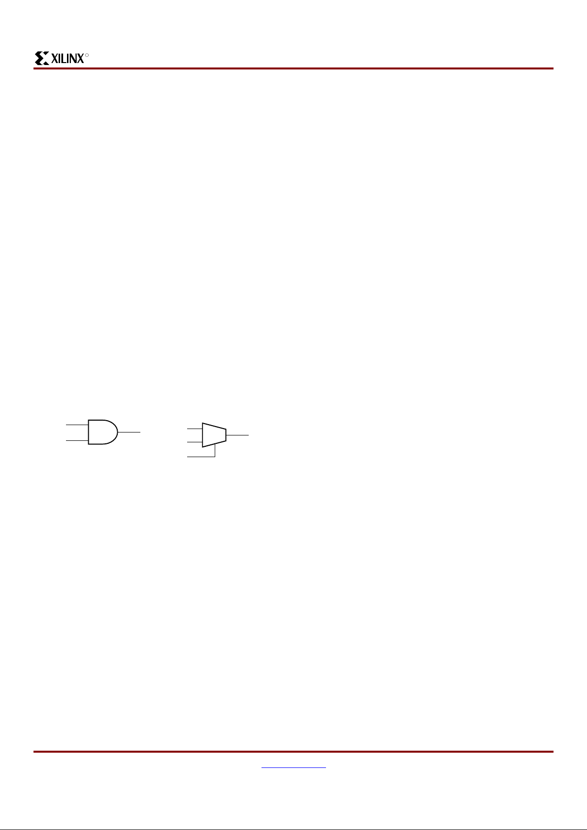
Table 11: Three-State Buffer Functionality
IN T OUT
X1Z
IN 0 IN
Figure 18: 3-state Buffers Implement a Multiplexer
D
N
D
C
D
B
D
A
ABCN
Z = (DA • A) + (DB • B) + (DC • C) + (DN • N)
~100 kΩ
"Weak Keeper"
DS060_18_080400
BUFT BUFT BUFT BUFT
Spartan and Spartan -XL Families Field Programm able Gate Arrays
20 www.xilinx.com DS060 (v1.6) September 19, 2001
1-800-255-7778 Product Speci fication
R
On-Chip Oscillator
Spartan/XL devices include an internal oscillator. This oscillator is used to clock the power-on time-out, for configuration memory clearing, and as the source of CCLK in Master
configuration mode. The oscillator runs at a nominal 8 MHz
frequency that varies with process, V
CC
, and temperature.
The output frequency falls between 4 MHz and 10 MHz.
The oscillator o utput is opt ionally available after configura-
tion. Any two of four resynchronized taps of a built-in divider
are also available. The se taps are at the fourth, ninth, fourteenth and nineteent h bits of the divider. Therefore, if the
primary oscillator outpu t is running at the nominal 8 MHz,
the user has access to an 8-MHz clock, plus any two of
500 kHz, 16 kHz, 490 Hz and 15 Hz. These frequencies
can vary by as much as -50% or +25%.
These signals can be accessed by placing the OSC4 library
element in a schematic or in HDL code. The oscillator is
automatically disabled after configuration if the OSC4 symbol is not used in the design.
Global Signals: GSR and GTS
Global Set/Reset
A separate Global Set/Reset line, as shown in Figure 3,
page 5 for the CLB and Figure 5, page 6 for the IOB, sets or
clears each flip-flop during power-up, reconfiguration, or
when a dedicated Reset net is driven active. This global net
(GSR) does not compete with other routing resources; it
uses a dedicated distribution network.
Each flip-flop is configured as either globally set or reset in
the same way that the local set/reset (SR) is specified.
Therefore, if a fli p-flop is se t by SR, it is also s et by GSR.
Similarly, if in reset mode, it is reset by both SR and GSR.
GSR can be driven from any user-programmable pin as a
global reset input. To use this global net, place an input pad
and input buffer in the schematic or HDL code, driving the
GSR pin of the STARTUP symbol. (See Figure 19.) A spe-
cific pin location can be assigned to this input using a LOC
attribute or proper ty, just as with any other u ser-programmable pad. An inverter can optionally be inserted after the
input buffer to invert the sen se of the GS R signal. Alter natively, GSR can be driven from any internal node.
Global 3-State
A separate Global 3-state line (GTS) as shown in Figure 6,
page 7 forces all FPGA outputs to the high-impedance
state, unless boundary scan is enabled and is executing an
EXTEST instruction. GTS does not compete with other routing resources; it uses a dedicated distribution network.
GTS can be driven from any user-programmable pin as a
global 3-state input. To use this global net, place an inp ut
pad and input buffer in the schematic or HDL code, driving
the GTS pin of the STARTUP symbol. This is similar to what
is shown in Figure 19 for GSR except the IBUF would be
connected to GTS. A spec ific pin location can be assign ed
to this input using a L OC attribute or proper ty, just as with
any other user-programmable pad. An inverter can optionally be inserte d after the input buffer to inver t the sense of
the Global 3-state signal. Alternatively, GTS can be driven
from any internal node.
Boundary Scan
The "bed of nails" has been the traditional method of testing
electronic assemblies. This approach has become less
appropriate, due to closer pin spacing and more sophisticated assembly methods like surface-mount technology
and multi-layer boards. The IEEE Boundary Scan Standard
1149.1 was developed to facilitate board-level testing of
electronic assemblies. Design and test engineers can
embed a standard test logic structure in their device to
achieve high fault coverage for I/O and internal logic. This
structure is easily implemented with a four-pin interface on
any boundary scan compatible device. IEEE 1149.1-compatible devices may be serial daisy-chained together, connected in parallel, or a combination of the two.
The Spartan and Spartan-XL families implement IEEE
1149.1-compatible BYPASS, PRELOAD/SAMPLE and
EXTEST boundar y scan instructions. When the boundary
scan configuration option is selected, three normal user I/O
pins become dedic ated inputs for these functions. Another
user output pin becomes the dedicated boundary scan output. The details of how to enable this circuitry are covered
later i n this section .
By exercising these input signals, the user can serially load
commands and data into these devices to control the driving
of their outputs and to examine their inputs. This m et hod is
an improvement over bed-of-nails testing. It avoids the need
to over-drive device out puts, and it reduces the user interface to four pins. An optional fifth pin, a reset for the control
logic, is described in the standard but is not implemented in
the Spartan/X L devices.
The dedicated on-chip logic imp lement ing the IE E E 1 149.1
functions includes a 16-state m ac hine, an in stru ction register and a num ber of data registers. The functional d etails
can be found in the IEEE 1149.1 specification and are also
discussed in the Xilinx application note: "Boundary S can i n
FPGA Devices."
Figure 19: Schema tic Symbo ls for Global Set/Reset
PAD
IBUF
GSR
GTS
CLK
DONEIN
Q1, Q4
Q2
Q3
STARTUP
DS060_19_080400

Spartan and Spartan -XL Families Field Programmabl e Gate Arrays
DS060 (v1.6) September 19, 2001 www.xilinx.com 21
Product Speci fication 1-800-255-7778
R
Figure 20 is a diagram of the Spartan/XL boundar y scan
logic. It includes three b its of Data Register per IOB, the
IEEE 1149.1 Test Access Port controller, and the Instruction
Register with decodes.
Spartan/XL devices can also be configured through the
boundary scan logic. See Configuration Through the
Boundary Scan P i ns, page 37.
Data Registers
The primary data register is the boundary scan register. For
each IOB pin in the FPGA, bonded or not, it includes three
bits for In, Out and 3-state Control. Non-IOB pins have
appropriate par tial bit population for In or Out only. PROGRAM, CCLK an d DONE are not included i n t he boundary
scan register. Each EXTEST CAPTURE-DR state captures
all In, Out, and 3-state pins.
The data register also includes the following non-pin bits:
TDO.T, and TDO.O, which are always bits 0 and 1 of the
data register, respectively, and BSCANT.UPD, which is
always the last bit of the data register. These three boundary scan bits are special -purpose Xilinx test signals .
The other standard data register is the single flip-flop
BYPASS register. It synchronizes data being passed
through the FPGA to the next downstream boundary scan
device.
The FPGA provides two additional data registers that can
be specified using t he BSCAN macro. The FPG A provides
two user pins (BSCAN.SEL1 and BSCAN.SEL2) which are
the decodes of two user instructions. For these instructions,
two corresponding pins (BSCAN.TDO1 and BSCAN.TDO2)
allow user scan data to be shifted out on TDO. The data
register clock (BSCAN.DRCK) is available for control of test
logic which the user may wish to implement with CLBs. The
NAND of TCK and RUN-TEST-IDLE is also provided
(BSCAN.IDLE).
Instruction Set
The Spartan/XL boundary scan instruction set also includes
instructions to c onfigure the device and rea d back the configuration data. The instruction set is coded as shown in
Table 12.
Spartan and Spartan -XL Families Field Programm able Gate Arrays
22 www.xilinx.com DS060 (v1.6) September 19, 2001
1-800-255-7778 Product Speci fication
R
Figure 20: Spartan/XL Boundar y Scan Logic
D Q
D Q
IOB
IOB
IOB
IOB
IOB
IOB
IOB
IOB
IOB
IOB
IOB
IOB
IOB
M
U
X
BYPASS
REGISTER
IOB IOB
TDO
TDI
IOB IOB IOB
1
0
1
0
1
0
1
0
1
0
sd
LE
DQ
D Q
D Q
1
0
1
0
1
0
1
0
DQ
LE
sd
sd
LE
DQ
sd
LE
DQ
IOB
D Q
1
0
DQ
LE
sd
IOB.T
DATA IN
IOB.I
IOB.Q
IOB.T
IOB.I
SHIFT/
CAPTURE
CLOCK DATA
REGISTER
DATAOUT UPDATE EXTEST
DS060_20_080400
INSTRUCTION REGISTER
Spartan and Spartan -XL Families Field Programmabl e Gate Arrays
DS060 (v1.6) September 19, 2001 www.xilinx.com 23
Product Speci fication 1-800-255-7778
R
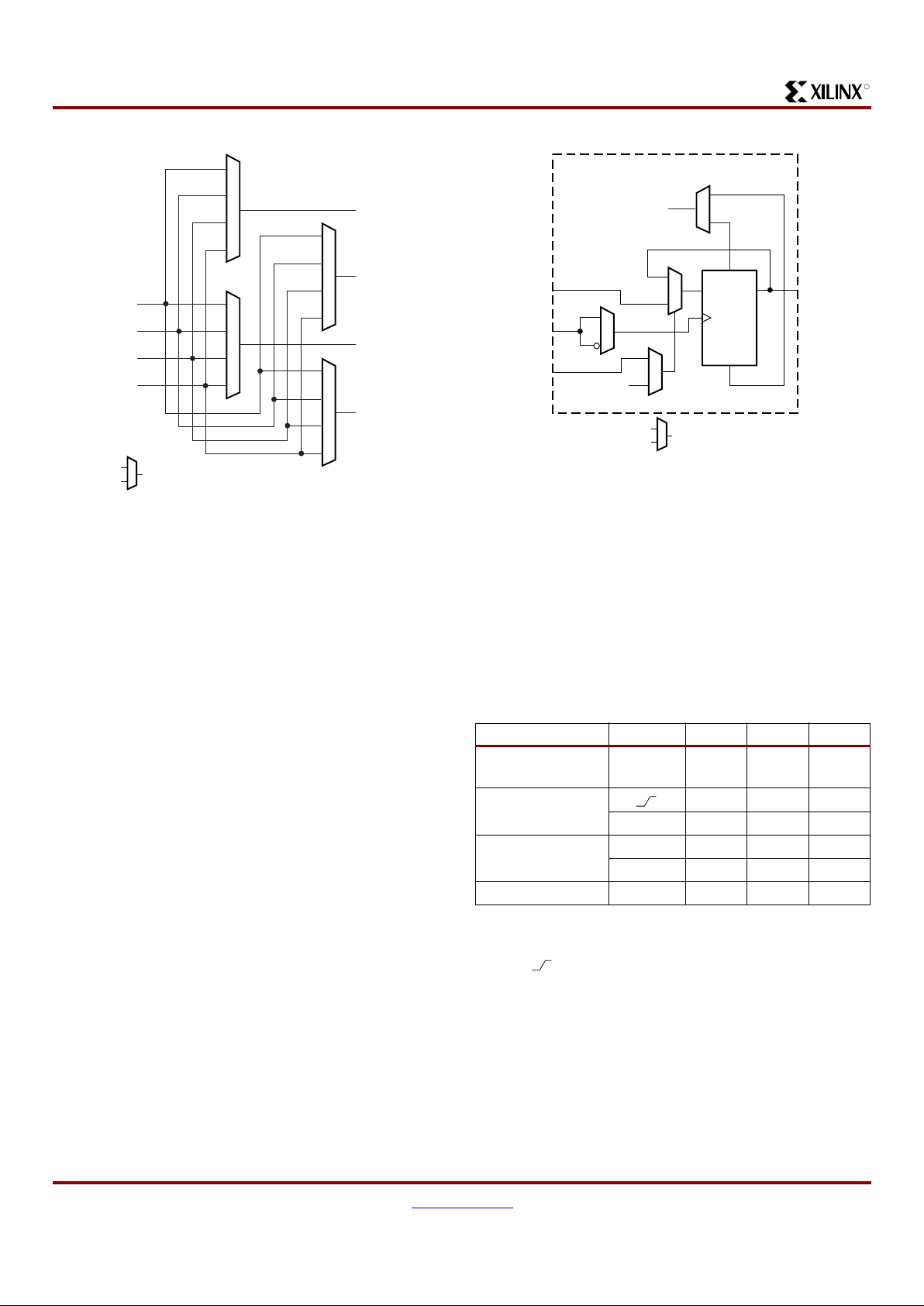
Bit Sequence
The bit sequence within each IOB is: In, Out, 3-state. The
input-only pins contribute only the In bit to the boundary
scan I/O data register, while the output-only pins contributes
all three bits.
The first two bits in the I/O data register are TDO.T and
TDO.O, which can be us ed for the capture of interna l signals. The final bit is BSCANT.UPD, which can be used to
drive an internal net . The se locat ions are primarily u sed by
Xilinx for internal test ing.
From a cav ity-up view of the chip (as shown in the FPGA
Editor), starting in the upper right chip corner, the boundary
scan data-register bits are ordered as s hown in Figure 21.
The device-specific pinout tables for the Spartan/XL devices
include the boundary scan locations for each IOB pin.
BSDL (Boundary Scan Description Language) files for
Spart an/XL devices are available on the Xilinx website in
the File Download area. Note that the 5V S partan devices
and 3V Spartan-XL devices have different BSDL files.
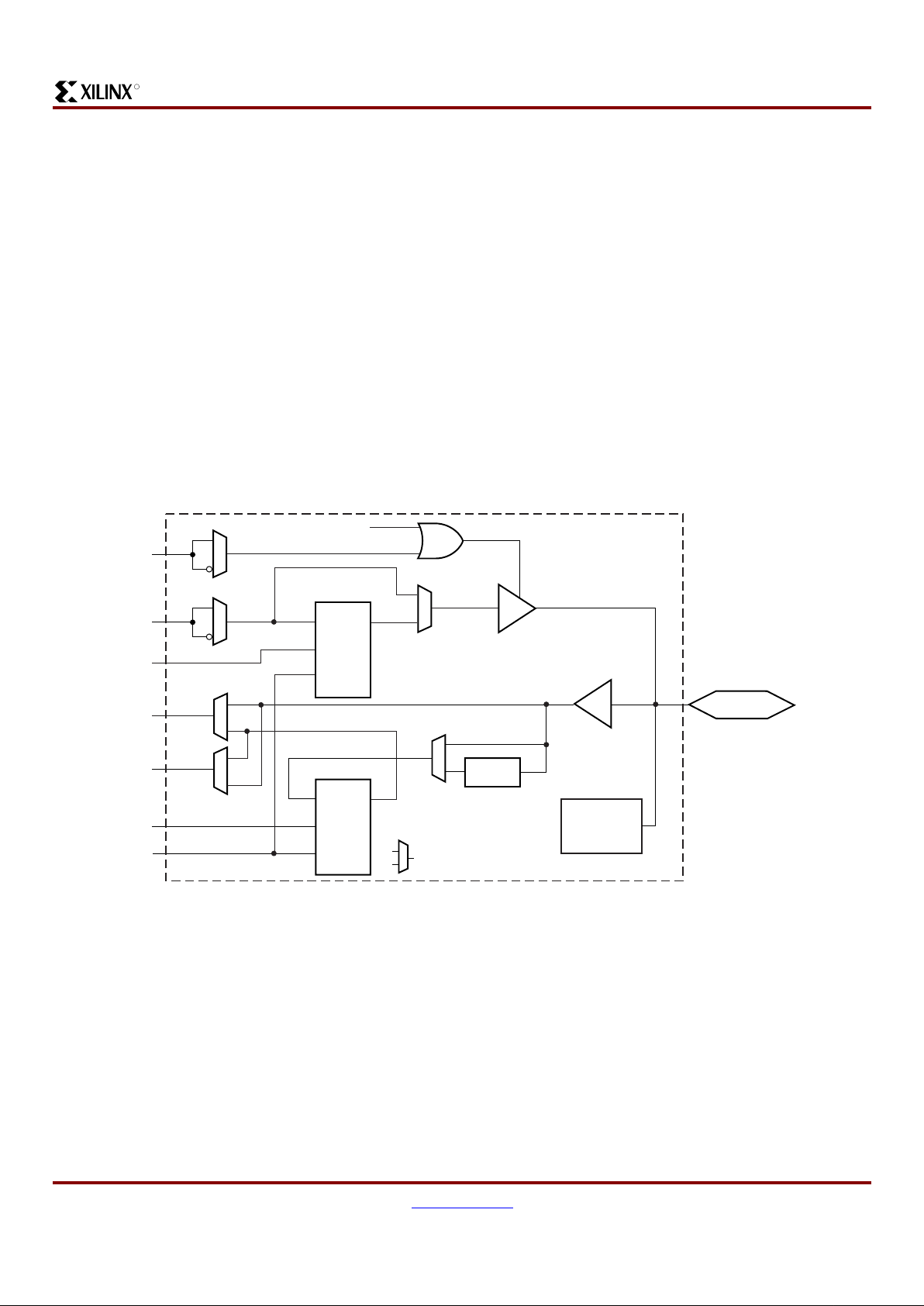
Including Boundary Scan in a Design
If boundary scan is only to be used during configuration, no
special schematic el ements need be included in the schematic or HDL code. In this case, the special boundary scan
pins TDI, TMS, TCK and TDO can be us ed for user functions after configuration.
To indicate that boundary scan remain enabled after configuration, place the BSCAN library s ymbol and connect the
TDI, TMS, TCK and TDO pad sy mbols to the appropriate
pins, as shown in Figure 22.
Table 12: Boundary Sc a n In st ructions
Instruction
Test
Selected
TDO
Source
I/O Data
SourceI2 I1 I0
0 0 0 EXTEST DR DR
0 0 1 SAM PLE/
PRELOAD
DR Pin/Logic
0 1 0 USER 1 BSCAN.
TDO1
User Logic
0 1 1 USER 2 BSCAN.
TDO2
User Logic
1 0 0 READBACK Readback
Data
Pin/Logic
1 0 1 CONFIGURE DOUT Disabled
1 1 0 IDCODE
(Spartan-XL
only)
IDCODE
Register
-
1 1 1 BYPASS Bypass
Register
-
Figure 21: Boundary Sc a n Bit Sequence
Figure 22: Boundary Scan Schematic Example
Bit 0 ( TDO end)
Bit 1
Bit 2
TDO.T
TDO.O
Top-edge IOBs (Right to Left)
Left-edge IOBs (Top to Bottom)
MODE.I
Bottom-edge IOBs (Left to Right)
Right-edge IOBs (Bottom to Top)
BSCANT.UPD
(TDI end)
DS060_21_080400
TDI
TMS
TCK
TDO1
TDO2
TDO
DRCK
IDLE
SEL1
SEL2
TDI
TMS
TCK
TDO
BSCAN
To User
Logic
IBUF
Optional
From
User Logic
To User
Logic
DS060_22_080400
Spartan and Spartan -XL Families Field Programm able Gate Arrays
24 www.xilinx.com DS060 (v1.6) September 19, 2001
1-800-255-7778 Product Speci fication
R
Even if the boundar y scan s ymbol is used in a sc hematic,
the input pins TMS, TCK, and TDI can still be used as inputs
to be routed to internal logic. Care must be taken not to
force the chip into an undesired boundary scan state by
inadvertently applying boundary scan input patterns to
these pins. The simplest way to prevent this is to keep TMS
High, and then apply whatever signal is desired to TDI and
TCK.
Avoiding Inadvertent Boundary Scan
If TMS or TCK is used as user I/O, care must be taken to
ensure that at least one of these pins is held constant during
configuration. In some applications, a situa tion may occur
where TMS or TCK is driven during configuration. This may
cause the device to go into boundary scan mode and di srupt the configuration process.
To prevent activation of boundary scan during configuration,
do either of the following:
• TMS: Tie High to put the Test Access Port controller
in a benign RESET state.
• TCK: Tie High or Low—do not toggle this clock input.
For more information regarding boundary scan, refer to the
Xilinx Application Note, "Boundary Scan in FPGA Devices. "
Boundary Scan Enhancements (Spartan-XL Only)
Spartan-XL devices have improved boundary scan functionality and performance in the following areas:
IDCODE: The IDCODE register is suppor ted. By us ing the
IDCODE, the device connected to the JTAG port can be
determined. The use of the IDCODE enables selective configuration dependent on the FPGA found.
The IDCODE register has the following binary format:
vvvv:ffff:fffa:aaaa:aaaa:cccc:cccc:ccc1
where
c = the company code (49h for Xilinx)
a = the array dimension in CLBs (ranges from 0Ah for
XCS05XL to 1Ch for XCS40XL)
f = the family code (02h for Spartan-XL family)
v = the die version number (currently 0h)
Configuration State: The configuration state is availab le to
JTAG controllers.
Configuration Disable: The JTAG port can be prevented
from configuring the FPGA.
TCK Startup: TCK can now be used to clock the start-up
block in addition to other user clocks.
CCLK Holdoff: Changed the requirement for Boundary
Scan Configure or EXTEST to be issued prior to the release
of INIT pin and CCLK cycling.
Reissue Configure: The Boundary Scan Configure can be
reissued to recover from an unfinished attempt to configure
the device.
Bypass FF: Bypass FF and IOB is modified to provide
DRCLOCK only during BYPASS for the bypass flip-flop, and
during EXTEST or SAMPLE/PRELOAD for the IOB register .
Power-Down (Spartan-XL Only)
All Spartan/XL devices use a combination of efficient segmented routing and advanced process technology to provide low power consumption under all conditions. The 3.3V
Spartan-XL family adds a dedicated active Lo w po wer-down
pin (PWRDWN
) to reduce supp ly current t o 100 µA typical.
The PWRDWN
pin takes advantage of one of the unused
No Connect locations on the 5V Spar tan device. The us er
must de-select the "5V Tolerant I/Os" option in th e Configurat io n Options to ac hi eve th e s pe c ified P o w er D o w n c urrent.
The PWRDWN
pin has a default internal pull-up resistor,
allowing it to be left unconnected if unused.
V
CC
must continue to be supplied during Power-down, and
configuration data is maintained. When the PWRDWN
pin is
pulled Low, the input and output buffers are disabled. The
inputs are internally forced to a logic Low level, i ncluding the
MODE pins, DONE, CCLK, and TDO, and all internal
pull-up resistors are turned off. The PROGRAM
pin is not
affected by Power Down. The GSR net is ass erted during
Power Down, initializing all the flip-flops to their start-up
state.
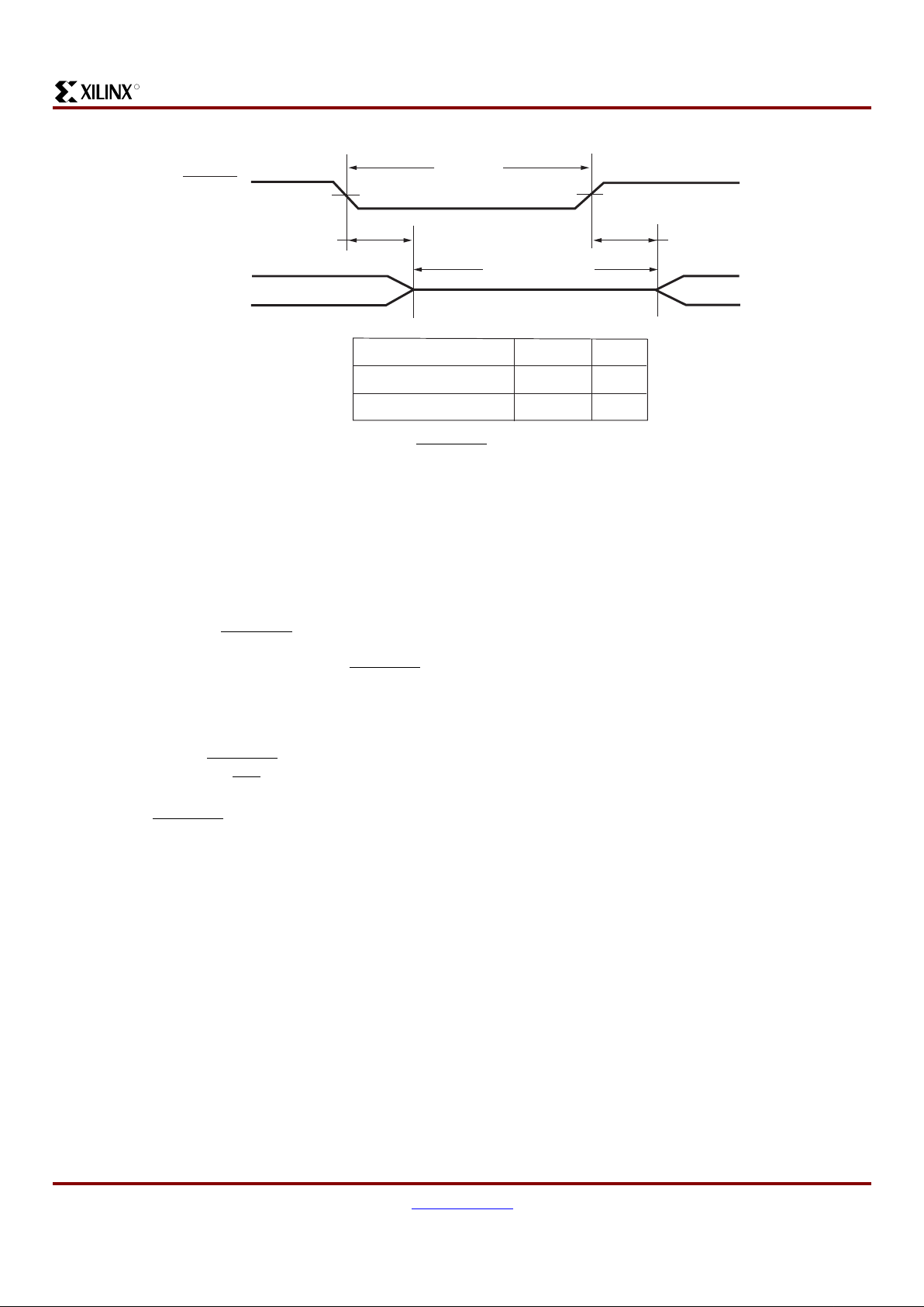
PWRDWN
has a minimum pulse width of 50 ns (Figure 23).
On ente ring the Power-down stat e, the inputs w ill be disabled and the flip-flops set/reset, and then the outputs are
disabled about 10 ns later. The user may prefer to assert the
GTS or GSR signals before PWRDWN
to affect the order of
events. When the PWRDWN
signal is returned High, the
inputs will be enabled first, followed immediately by the
release of the GSR signal initializing the flip-flops. About 10
ns later, the outputs will be enabled. Allow 50 ns after the
release of PWRDWN
before using the dev ice.
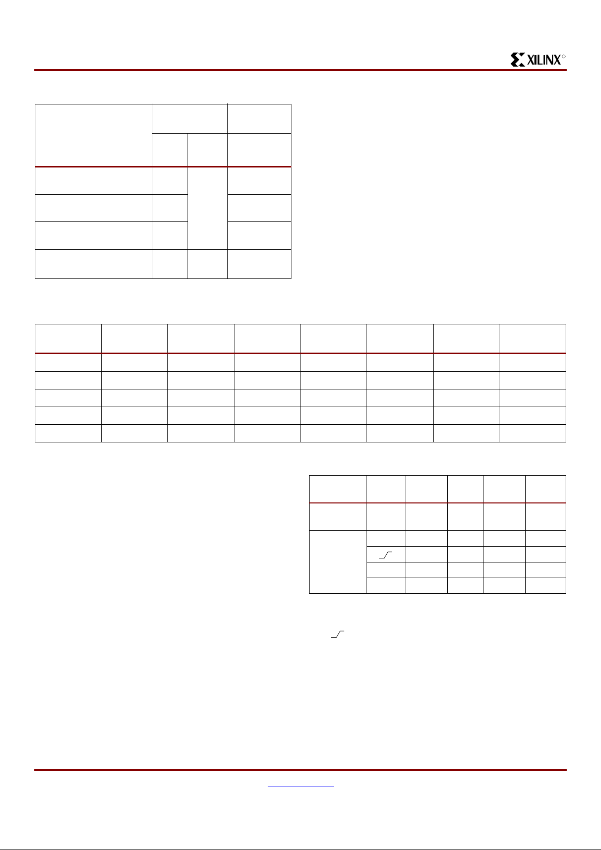
Table 13: IDCODEs Assigned to Spartan-XL FPGAs
FPGA IDCODE
XCS05XL 0040A093h
XCS10XL 0040E093h
XCS20XL 00414 093h
XCS30XL 00418 093h
XCS40XL 0041C093h
Spartan and Spartan -XL Families Field Programmabl e Gate Arrays
DS060 (v1.6) September 19, 2001 www.xilinx.com 25
Product Speci fication 1-800-255-7778
R
Power-down retains the configuration, but loses all data
stored in the device flip-flops. All inputs are interpreted as
Low, but the internal combin atorial logic is fully functional.
Make sure that the combination of all inputs Low and all
flip-flops set or reset in your design will not generate internal
oscillations, or create permanent bus contention by activating internal bus drivers with conflicting data onto the same
long line.
During configuration, the PWRDWN
pin must be High. If the
Power Down state is entered before or during configuration,
the device will restart configuration once the PWRDWN
signal is removed. Note that the configuration pins are affected
by Power Down and may not reflect their normal function. If
there is an external pull-up res istor on the DONE pin, i t w ill
be High during Power Down even if the device is not yet
configured. Similarly, if PWRD WN
is asserted before config-
uration is completed, the INIT
pin will not indicate status
information.
Note that the PWRDWN
pin is not part of the Boundary
Scan chain. Therefore, the Spartan-XL family has a separate set of BSDL files than the 5V Spartan family. Boundary
scan logic is not usable during Power Down.
Configuration and Test
Configuration is the proces s of l oadin g design-specific programming data into one or more FPG As to define the functional operation of the internal blocks and their
interconnections. This is somewhat like loading the command registers of a programmable peripheral chip.
Spartan/XL devices use several hundred bits of configuration data per CLB and its associated interconnects. Each
configuration bit defines the state of a static memory cell
that controls either a function look-up table bit, a multiplexer
input, or an interconnect pass transistor. The Xilinx development system translates the design into a netlist file. It automatically partitions, places and routes the logic and
generates the configuration data in PROM format.
Configuration Mode Cont ro l
5V Spartan devices have two configuration modes.
• MODE = 1 sets Slave Serial mode
• MODE = 0 sets Master Serial mode
3V Spartan-XL devices have three configuration modes.
• M1/M0 = 11 sets Slave Serial mode
• M1/M0 = 10 sets Master Seria l mode
• M1/M0 = 0X sets Express mod e
In addition to these modes, the device can be configured
through the Boundary Scan logic (See "Configuration
Through the Boundary Scan Pins" on page 37.).
The Mode pins are sampled prior to starting configuration to
determine the configuration mode. After configuration,
these pin are unused. The Mode pins have a weak pull-up
resistor turned o n during configuration. With t he M ode p ins
High, Slave Serial mode is selected, which is the most popular configuration mode. Therefore, for the most common
configuration mode, the Mode pins can be left unconnected.
If the Master Serial mode is desired, the MODE/M0 pin
should be connected directly to GND, or through a
pull-down resistor of 1 KΩ or less.
Figure 23: PWRDWN
Puls e Timing
Power Down Mode
50 ns
50 ns
T
PWDW
T
PWD
T
PWDW
Outputs
PWRDWN
Description
Power Down Time
Power Down Pulse Width
Symbol
Min
50 ns
50 ns
DS060_23_041901

Spartan and Spartan -XL Families Field Programm able Gate Arrays
26 www.xilinx.com DS060 (v1.6) September 19, 2001
1-800-255-7778 Product Speci fication
R
During configuration, some of the I/O pins are used temporarily for the configuration process. All pins used during configuration are shown in Table 14 and Table 15.
Table 14: Pin Functions During Con f ig uration
(Spartan family only)
Configuration Mo de ( M OD E Pi n)
User
Operation
Slave Serial
(High)
Master Serial
(Low)
MODE (I) MODE (I) MODE
HDC (High) HDC (High) I/O
LDC
(Low) LDC (Low) I/O
INIT
INIT I/O
DONE DONE DONE
PROGRAM (I) PROGRAM (I) PROGRAM
CCLK (I) CCLK (O) CCLK (I)
DIN (I) DIN (I) I/O
DOUT DOUT SGCK4-I/O
TDI TDI TDI-I/O
TCK TCK TCK-I/O
TMS TMS TMS-I/O
TDO TDO TDO-(O)
ALL OTHERS
Notes:
1. A shaded table cel l re presents the internal pull-up used
before and duri ng configuration.
2. (I) represents an input; (O) represents an output.
3.
INIT is an open-drain output during configuration.
Table 15: Pin Functions During Configuration
(Spartan-XL family only)
CONFIGURATION MODE <M1:M0>
User
Operation
Slave
Serial
[1:1]
Master
Serial
[1:0]
Express
[0:X]
M1 (High) (I) M1 (High) (I) M1(Low) (I) M1
M0 (High) (I) M0 (Low) (I) M0 (I) M0
HDC (High) HDC (High) HDC (High) I/O
LDC
(Low) LDC (Low) LDC (Low) I/O
INIT
INIT INIT I/O
DONE DONE DONE DONE
PROGRAM
(I)
PROGRAM
(I)
PROGRAM
(I)
PROGRAM
CCLK (I) CCLK (O) CCLK (I) CCLK (I)
DATA 7 (I) I/O
DATA 6 (I) I/O
DATA 5 (I) I/O
DATA 4 (I) I/O
DATA 3 (I) I/O
DATA 2 (I) I/O
DATA 1 (I) I/O
DIN (I) DIN (I) DATA 0 (I) I/O
DOUT DOUT DOUT GCK6-I/O
TDI TDI TDI TDI-I/O
TCK TCK TCK TCK-I/O
TMS TMS TMS TMS-I/O
TDO TDO TDO TDO-(O)
CS1 I/O
ALL
OTHERS
Notes:
1. A shaded table cel l represents the internal pull -up used
before and duri ng configuration.
2. (I) represents an input; (O) represents an output.
3.
INIT is an open-drain output during configuration.

Spartan and Spartan -XL Families Field Programmabl e Gate Arrays
DS060 (v1.6) September 19, 2001 www.xilinx.com 27
Product Speci fication 1-800-255-7778
R
Master Serial Mo de
The Master serial mode uses an internal oscillator to generate a Configuration Clock (CCLK) for driving potential slave
devices and the Xilinx serial-configuration PROM
(SPROM). The CCLK speed is selectable as either 1 MHz
(default) or 8 MHz. Configuration always starts at the default
slow frequency , then can switch to the higher frequency during the first frame. Freque nc y tolerance is –50% to +25%.
In Master Serial mode, the CCLK output of the device drives
a Xilinx SPROM that feeds the FPGA DIN input. Each rising
edge of the CCLK output increments the Serial PROM internal address counter. The next data bit is put on the SPROM
data output, connected to the FPGA DIN pin. The FPGA
accepts this data on the subsequent rising CCLK edge.
When used in a daisy-chain configuration the Master Serial
FPGA is placed as the first device in the chain and is
referred to as the lead FPGA. The lead FPG A presents the
preamble data, and all data t hat overflows the lead device,
on its DOUT pin. There is a n internal pip eline delay of 1.5
CCLK periods, which means that DOUT changes on the
falling CCLK edge, and the next FPGA in the daisy chain
accepts data on the subsequent rising CCLK edge. See the
timing diagram in Figure 24.
In the bitstream generation software, the user can specify
Fast Configuration Rate, which, starting sev eral bi ts into the
first frame, increases the CCLK frequency by a factor of
eight. For actual timing values please refer to the specification section. Be sure that the serial PROM and slaves are
fast enough to support this data rate. Devices such as
XC3000A and XC3100A do not support the Fast Configuration Rate option.
The SPROM CE input can be driven from either LDC
or
DONE. Using LDC
avoids potential contention on the DIN
pin, if this pin is configured as user I/O, but LDC
is then
restricted to be a permanently High user output after configuration. Using DONE can also avoid contention on DIN, provided the Early DONE option is invoked.
Figure 25 shows a full master/slave system. The leftmost
device is in Master Serial mode, all other devices in the
chain are in Slave Serial mode.
Slave Serial Mode
In Slave Serial mode, the FPGA receives serial configuration data on the rising ed ge of CCLK and, after lo ading its
configuration, passes additional data out, resynchronized
on the next falling edge of CCLK.
In this mode, an external signal drives the CCLK input of the
FPGA (most often f rom a Mas ter Seria l device). The serial
configuration bitstream must be available at the DIN input of
the lead FPGA a short setup time before each ris ing CCL K
edge.
The lead FPGA then prese nts the preamble data—and all
data that overflows the lead device—on its DOUT pin. There
is an interna l del ay of 0.5 CCLK periods, which means that
DOUT changes on the falling CCLK edge, and the next
FPGA in the daisy chain accept s data on the subsequent
rising CCLK edge.
Figure 25 shows a full master/slave system. A Spartan/XL
device in Slave Serial mode should be connected as shown
in the third device from the left.
Figure 24: Master Serial Mode Programming Switching Characteristics
Serial Data In
CCLK
(Output)
Serial DOUT
(Output)
T
DSCK
n n + 1 n + 2
n – 3n – 2n – 1n
T
CKDS
DS060_24_080400
Notes:
1. At power-up, V
CC
must rise from 2.0V to VCC min in less than 25 ms, otherwise
delay configuration by pulling PROGRAM Low until VCC is valid.
2. Master Serial mode timing is based on testing in slave mode.
Symbol Description Min Units
CCLK
T
DSCK
DIN setup 20 ns
T
CKDS
DIN hold 0 ns

Spartan and Spartan -XL Families Field Programm able Gate Arrays
28 www.xilinx.com DS060 (v1.6) September 19, 2001
1-800-255-7778 Product Speci fication
R
Slave Serial is the default mode if the Mode pins are left
unconnected, as they have weak pull-up resistors during
configuration.
Multiple slave devices with identical configurations can be
wired with parallel DIN inp uts. In this w ay, mult iple devices
can be configured simultaneously .
Serial Daisy Chain
Multiple devices with different configurations can be connected together in a "daisy chain," and a singl e combined
bitstream used to configure the chain of slave dev i ces.
To configure a daisy chain of devices, wire the CCLK pins of
all devices in parallel, as shown in Figure 25. Connect the
DOUT of each device to the DIN of the next. The lead or
master FPGA and following slaves each passes resynchronized configuration data coming from a s ingle source. The
header data, including the length count, is passed through
and is captured by each FPGA when it recognizes the 0010
preamble. Following the length-count data, each FPGA outputs a High on DOUT until it has received its required number of data frames.
After an FPGA has received its configuration data, it passes
on any additional frame start bits and configuration data on
DOUT. When the total number of configuration clocks
applied after memory initialization equals the value of the
24-bit length count, the FPGAs begin the start-up sequence
and become operational together. FPGA I/O are n ormally
released two CCLK cycles af ter the last configuration bit is
received.
The daisy-chained bitst ream is not simply a concatenation
of the individual bitstreams. The PROM File Formatter must
be used to combine the bitstreams for a daisy-chained configuration.
Figure 25: Master/Slave Serial Mode Circuit Diagram
Spartan
Master
Seria
l
Spartan
Slave
FPGA
Slave
Xilinx SPROM
PROGRAM
Note:
M2, M1, M0 can be shorted
to V
CC
if not used as I/O
MODE
DOUT
CCLK
CLK
V
CC
V
CC
+5V
DATA
CE
CEO
V
PP
RESET/OE
DONE
DIN
LDC
INIT INIT
DONE
PROGRAM
PROGRAM
D/P
INIT
RESET
CCLK
DIN
CCLK
DIN
DOUT DOUT
MODE
M1
M0
M2
(Low Reset Option Used)
3.3K
3.3K
3.3K
3.3K
DS060_25_061301
N/C

Spartan and Spartan -XL Families Field Programmabl e Gate Arrays
DS060 (v1.6) September 19, 2001 www.xilinx.com 29
Product Speci fication 1-800-255-7778
R
Express Mode (Spartan-XL only)
Express mode is similar to Slave Serial mode, except that
data is processed one byte per CCLK cycle instead of one
bit per CCLK cycle. An external source is used to drive
CCLK, while byte-wide data is loaded direct ly into the configuration data shift registers (Figure 27). A CCLK frequency of 1 MHz is equivalent to a 8 MHz serial rate,
because eight bits of configuration data are loaded per
CCLK cycle. Express mode does not support CRC error
checking, but does support cons tant-field error c hecking. A
length count is not used in Express mode.
Express mode must be specified as an option to the development system. The Express m ode bitstream is not compatible with the other configuration modes (see Table 16,
page 32.) Express mode is selected by a <0X> on the Mode
pins (M1, M0).
The first byte of parallel c onfiguration data must be av ailabl e
at the D inputs of the FPGA a short setup time before the
second rising CCLK edge. Subsequent data bytes are
clocked in on each consecutive rising CCLK edge
(Figure 28).
Pseudo Daisy Chain
Multiple devices with different configurations can be configured in a pseudo daisy chain provided that all of the devices
are in Express mode. A single com bined b itstream is used
to configure the chain of Express mode devices. CCLK pins
are tied together and D0-D7 pi ns are tied together for all
devices along the chain. A status signal is passed from
DOUT to CS1 of successive devices along the chain. F rame
data is accepted only when CS1 is High and the device’s
configuration memor y is not already full. The lead device in
the chain has its CS1 input tied High (or floating, since there
is an internal pull-up). The st atus pin DOUT is pulled Low
after the header is received by all devices, and remains Low
until the device’s configuration memory is full. DOUT is then
pulled High to signal the next device in the chain to accept
the configuration data on the D0-D7 bus.
The DONE pins of all devices in the chain should be tied
together, with one or more active internal pull-ups. If a large
number of devices are included in the chain, deactivate
some of the internal pull-ups, since the Low-driving DONE
pin of the last device in the chain must sink the current from
all pull-ups in the chai n. The DONE pull-up i s activated by
default. It can be deactivated using a development system
option.
The requirement that all DONE pins in a daisy chain be
wired together applies only to Express mode, and on ly if all
devices in the chain a re to become act ive simultaneously.
All Spartan-X L devices in Express mode are synchronized
to the DONE pin. User I/Os for each device become active
Figure 26: Slave Serial Mode Programming Switching Characteristics
T
CCH
Bit n Bit n + 1
Bit nBit n – 1
T
CCO
T
CCL
T
CCD
T
DCC
DIN
CCLK
DOUT
(Output)
DS060_26_080400
Symbol Description Min Max Units
T
DCC
CCLK
DIN setup 20 - ns
T
CCD
DIN hold 0 - ns
T
CCO
DIN to DOUT - 30 ns
T
CCH
High time 40 - ns
T
CCL
Low time 40 - ns
F
CC
Frequency - 10 MHz
Notes:
1. Configuration mus t be delay ed until the INIT
pins of all daisy- chained FPGAs are
High.

Spartan and Spartan -XL Families Field Programm able Gate Arrays
30 www.xilinx.com DS060 (v1.6) September 19, 2001
1-800-255-7778 Product Speci fication
R
after the DONE pin for that device goes High. (Th e exact
timing is determined by development system options.)
Since the DONE pin is open-drain and does not drive a High
value, tying the DONE pins of all devices together prevents
all devices in the chain from going High until the last device
in the chain has completed its configuration cycle. If the
DONE pin of a device is left unconnected, the device
becomes active as soon as that device has been configured. Because only Spartan-XL, XC4000XLA/XV, and
XC5200 devices support Express mode, only these devices
can be used to form an Express mode daisy chain.
Figure 27: Express Mode Circuit Diagram
INIT
CCLK CCLK
Spartan-XL
M0 M1
CS1
D0-D7
DATA BUS
PROGRAM
INIT
CCLK
PROGRAM
INIT
DOUT
DONEDONE
DOUT
To Additional
Optional
Daisy-Chained
Devices
To Additional
Optional
Daisy-Chained
Devices
Optional
Daisy-Chained
Spartan-XL
M0 M1
VCC
V
CC
3.3K
CS1
D0-D7
PROGRAM
DS060_27_080400
8
8
8

Spartan and Spartan -XL Families Field Programmabl e Gate Arrays
DS060 (v1.6) September 19, 2001 www.xilinx.com 31
Product Speci fication 1-800-255-7778
R
Setting CCLK Frequency
In Master mode, CCLK can be generated in either of two
frequencies. In the default slow mode, the frequency ranges
from 0.5 MHz to 1.25 MHz for Spartan /XL devices. In fast
CCLK mode, the frequency ranges from 4 MHz to 10 MHz
for Spartan/XL devices. The frequency is changed to fast by
an option when running the bitstream generation software.
Data Stream Format
The data stream ("bitstream") format is identical for both
serial configuration modes, but different for the Spar tan-XL
Express mode. In Express mode, the device becomes
active when DONE goes High, therefore no length count is
required. Additionally, CRC error checking is not support ed
in Express mode. The data stream format is shown in
Table 16. Bit-serial data is rea d from left to right. Express
mode data is shown with D0 at the left and D7 at the right.
The configuration data stream begins with a string of eight
ones, a preamble code, followed by a 24-bit length count
and a separat or field of ones (or 24 fill bits, in Spar tan-XL
Express mode). This heade r is followed by the actual configuration data in frames. The length and number of frames
depends on the device type (see Table 17). Each frame
begins with a start fie ld and ends with an error check. In
serial modes, a postamble code is required to signal the end
of data for a single device. In all cases, additional start-up
bytes of data are required to provide four clocks for the startup sequence at the end of configuration. Long daisy chains
require additional startup bytes to shift the last data through
the chain. All start-up bytes are "don’t cares".
Figure 28: Express Mode Programming Switching Characteristics
DS060_28_080400
BYTE
0
CCLK
FPGA Filled
INIT
T
DC
T
CD
T
IC
D0-D7
DOUT
BYTE
1
BYTE
6
Header Received
Symbol Description Min Max Units
T
IC
CCLK
INIT
(High) setup time 5 - µs
T
DC
D0-D7 setup time 20 - ns
T
CD
D0-D7 hold time 0 - ns
T
CCH
CCLK High time 45 - ns
T
CCL
CCLK Low time 45 - ns
F
CC
CCLK Frequency - 10 MHz
Notes:
1.
If not driven by the preceding DOUT, CS1 must remain High until the
device is fully configured.

Spartan and Spartan -XL Families Field Programm able Gate Arrays
32 www.xilinx.com DS060 (v1.6) September 19, 2001
1-800-255-7778 Product Speci fication
R
Legend:
A selection of CRC or non-CRC error checking is allowed by
the bitstream generation software. The Spartan-XL Express
mode only supports non-CRC error checking. The
non-CRC error checking tests for a designated
end-of-frame field for each frame. For CRC error checking,
the software calculates a running CRC and inserts a unique
four-bit partial check at the end of each frame. The 11-bit
CRC check of the last frame of an F PGA includes the last
seven data bits.
Detection of an error results in the suspension of data loading before DONE goes High, and the pulling down of the
INIT
pin. In Master serial mode, CCLK continues to operate
externally. The user must detect INIT
and initialize a new
configuration by pulsing the PROGRAM
pin Low or cycling
V
CC
.
Cyclic Redundancy Check (CRC) for Configuration and Readback
The Cyclic Redundancy Check is a method of error detection in data transmission applications. Generally, the transmitting system performs a calculation on the serial
bitstream. The result of this calculation is tagged onto the
data stream as additional check bits. The receiving system
performs an identical calculation on the bitstream and compares the result with the received checksum.
Each data frame of the configuration bitstream has four
error bits at the end, as shown in Table 16. If a frame data
error is detected during the loading of the FPGA, the configuration process with a potentially corrupted bitstream is terminated. The FPGA pulls the INIT
pin Low and goes into a
Wait stat e.
Table 16: Spartan/XL Data Stream Formats
Data Type
Serial Modes
(D0...)
Express Mode
(D0-D7)
(Spartan-XL only )
Fill Byte 11111111b FF FF h
Preamble Code 001 0b 11 110010b
Length Count COUNT[23:0] COUNT[23:0]
(1)
Fill Bits 1111b Field Check
Code
- 11010010b
Start Field 0b 11111110b
(2)
Data Frame DATA[n–1:0] DAT A[n–1:0]
CRC or Constant
Field Check
xxxx (CRC)
or 0110b
11010010b
Extend Write
Cycle
- FFD2FFFFFFh
Postamble 01111111b Start-Up Bytes
(3)
FFh FFFFFFFFFFFFFFh
Unshaded Once per bitstream
Light Once per data frame
Dark Once per device
Notes:
1. Not used by configuration logic.
2. 11111111b for XCS40XL only.
3. Deve lopment system may add more start-up bytes.

Spartan and Spartan -XL Families Field Programmabl e Gate Arrays
DS060 (v1.6) September 19, 2001 www.xilinx.com 33
Product Speci fication 1-800-255-7778
R
During Readback, 11 bits of the 16-bit checksum are added
to the end of the Readback data stream. The checksum is
computed using the CRC-16 CCITT p olynomial, as shown
in Figure 29. The checksum consists of t he 11 most significant bits of the 16-bit code. A change in the checksum indicates a change in the Readback bitstream. A comparison to
a previous checksum is meaningful only if the readback
data is independent of the current device state. CLB outputs
should not be included (Readback Capture option not
used), and if RAM is present, the RAM content must be
unchanged.
Statistically, one error out of 2048 might go undetec ted.
Table 17: Spartan/XL Program Data
Device XCS05 XCS10 XCS20 XCS30 XCS40
Max System
Gates
5,000 10,000 20,000 30,000 40,000
CLBs
(Row x Col.)
100
(10 x 10)
196
(14 x 14)
400
(20 x 20)
576
(24 x 24)
784
(28 x 28)
IOBs 80 112 160 192 224
Part Number XCS05 XCS05XL XCS10 XCS10XL XCS20 XCS20XL XCS30 XCS30XL XCS40 XCS40XL
Supply Voltage 5V 3.3V 5V 3.3V 5V 3.3V 5V 3.3V 5V 3.3V
Bits per Frame 126 127 166 167 226 227 266 267 306 307
Frames 428 429 572 573 7 88 789 932 933 1, 076 1,077
Program Data 53,936 54,491 94,960 95,699 178,096 179,111 24 7,9 20 249,119 329,264 330,647
PROM Size
(bits)
53,984 54,544 95,008 95,752 178,144 179,160 247,968 249,168 329,312 330,696
Serial PROM 17S05 17S 05XL 17S 10 17S10XL 17S20 17 S20 XL 17S30 17S30XL 17S 40 17S40XL
Express Mode
PROM Size
(bits)
- 79,072 - 128,488 - 221,056 - 298,696 - 387,856
Notes:
1. Bits per F rame = (10 x number of rows) + 7 f or the top + 13 for the bottom + 1 + 1 start bit + 4 error check bi ts (+1 for Spartan-XL
device)
Number of Frames = (36 x number of columns) + 26 for the left edge + 41 for the right edge + 1 (+ 1 for Spartan-XL device)
Program Data = (Bits per Frame x Number of Frames) + 8 postamble bits
PROM Size = Program Data + 40 (header) + 8, rounded up to the nearest byte
2. The user can add more "1" bits as lead ing dummy bits in the header, or, i f CRC = of f, as trailing dummy bits at the end of any frame,
foll owing the four error check bits. Ho wever, the Length Count value must be adjusted for all such ex tra "one" bits, even for extr a
leading ones at the beginning of the header.
3. Express mode adds 57 (XCS05XL, XCS10XL), or 53 (XCS20XL, XCS30XL, XCS40XL) bits per fr am e, + additional start-up bits.

Spartan and Spartan -XL Families Field Programm able Gate Arrays
34 www.xilinx.com DS060 (v1.6) September 19, 2001
1-800-255-7778 Product Speci fication
R
Configuration Sequence
There are four major steps in the Spartan/XL power-up configuration sequence.
• Configuration Memory Clear
• Initialization
• Configuration
• Start-up
The full process is illustrated in Figure 30.
Configuration Memory Clear
When power is first applied or is reapplied to an FPG A, an
internal circuit forces initialization of the configuration logic.
When V
CC
reaches an operational level, and the circuit
passes the write and read test of a sample pair of configuration bits, a time delay is started. This time delay is nominally 16 ms. The delay is four times as long when in Master
Serial Mode to allow ample time for all slaves to reach a stable V
CC
. When all INIT pins are tied together, as recommended, the longest delay takes precedence. Therefore,
devices with different time delays can easily be mixed and
matched in a daisy chain.
This delay is applied only on power-up. It is not applied
when reconfiguring an FPGA by pulsing the PROGRAM
pin
Low. During this time delay, or as long as the PROGRAM
input is asserted, the configuration logic is held in a Configuration Memory Clear state. The configuration-memory
frames are consecutively initialized, using the internal oscillator.
At the end of each complete pass through the frame
addressing, the power-on time-o ut delay circuitry and the
level of the PROGRAM
pin are tested. If neither is asserted,
the logic initiates one additional clearing of the configuration
frames and then tests the INIT
input.
Initialization
During initialization and configuration, user pins HDC, LDC,
INIT
and DONE provide status outputs for the system inter-
face. The outputs LDC
, INIT and DONE are held Low a nd
HDC is held High starting at the initial application of power.
The open drain INIT
pin is released after the final initialization pass through the frame addresses. There is a deliberate delay before a Master-mode device recognizes an
inac tive INIT
. Two internal clocks after the INIT pin is recognized as High, the device samples the MODE pin to determine the configuration mode. The appropriate interface
lines become active and the configuration preamble and
data can be loaded.
Figure 29: Circuit for Generating CRC-16
0
X2
2
345678910111213 141
X15
X16
15
SERIAL DATA IN
1 01514131211109 8 7 651111
CRC – CHECKSUM
LAST DATA FRAME
START BIT
DS060_29_080400
Polynomial: X16 + X15 + X2 + 1
Readback Data Stream

Spartan and Spartan -XL Families Field Programmabl e Gate Arrays
DS060 (v1.6) September 19, 2001 www.xilinx.com 35
Product Speci fication 1-800-255-7778
R
Configuration
The 0010 preamble code indicates that the following 24 bits
represent the length count for serial modes. The length
count is the total number of configuration clo cks needed to
load the complete configuration data. (Four additional configuration clocks are required to complete the configuration
process, as discussed below.) After the preamble and the
length count have been passed through to any device in the
daisy chain, its DOUT is held High to preven t frame start
bits from reaching any daisy-chained devices. In Spartan-XL Express mode, the length count bits are ignored,
and DOUT is held Low, to disable the next device in the
pseudo daisy chain.
A specific configuration bit, early in the first frame of a master device, controls the configuration-clock rate and can
increase it by a factor of eight. Therefore, i f a f ast configuration clock is selected by the bitstream, the slower clock rate
is used until this configuration bit is detected.
Each frame has a star t field followed by the frame-configuration data bits and a frame error field. If a frame data error
is detected, the FPGA halts loading, and signals the error by
pulling the open-drain INIT
pin Low. After all configuration
frames have been loaded into an FPGA using a serial
mode, DOUT again follows the input data so that the
remaining data is passed on to the next device. In
Spartan-XL Express mode, when the first device is fully programmed, DOUT goes High to enable the next device in the
chain.
Delaying Configuration After Power-Up
There are two methods of delaying configuration after
power-up: put a logic Low on the PROGRAM
input, or pull
the bidirectional INIT
pin Low, using an open-collector
(open-drain) driver. (See Figure 30.)
A Low on the PROGRAM
input is the more radical
approach, and is recommended when the power-supply rise
time is excessive or poorly defined. As long as PROGRAM
is Low, the FPGA keeps clearing its configuration memory.
When PROGRAM
goes High, the configuration memo ry is
cleared one more time, followed by the beginning of configuration, provided the INIT
input is not externally held Low.
Note that a Low on the PROGRAM
input automatically
forces a Low on the INIT
output. The Spartan/XL PROGRAM pin has a permanent weak pull-up. Avoid holding
PROGRAM
Low for m ore than 500 µs.
Using an open-collector or open-drain driver to hold INIT
Low before the beginning of configuration causes the FPGA
to wait after completing the configuration memory clear
operation. When INIT
is no longer held Low externally, the
device determines its configuration mode by capturi ng the
state of the Mode pins, and is ready to start the configuration process. A master device waits up to an additional
300 µs to make sure that any slaves in the optional daisy
chain have seen that INIT
is High.
Figure 30: Power-up Configuration Sequence
INIT
High? if
Master
Sample
Mode Line
Load One
Configuration
Data Frame
Frame
Error
Pass
Configuration
Data to DOUT
V
CC
Valid
No
Yes
Yes
No
No
Yes
Operational
Start-Up
Sequence
No
Yes
~1.3 µs per Frame
Master Delays Before
Sampling Mode Line
Master CCLK
Goes Active
F
Pull INIT Low
and Stop
DS060_30_080400
EXTEST*
SAMPLE/PRELOAD
BYPASS
CONFIGURE*
(* if PROGRAM = High)
SAMPLE/PRELOAD
BYPASS
EXTEST
SAMPLE PRELOAD
BYPASS
USER 1
USER 2
CONFIGURE
READBACK
If Boundary Scan
is Selected
Configuration
memory
Full
CCLK
Count Equals
Length
Count
Completely Clear
Configuration Memory
Once More
LDC Output = L, HDC Output = H
Boundary Scan
Instructions
Available:
I/O Active
Keep Clearing
Configuration
Memory
Test MODE, Generate
One Time-Out Pulse
of 16 or 64 ms
PROGRAM
= Low
No
Yes
Yes

Spartan and Spartan -XL Families Field Programm able Gate Arrays
36 www.xilinx.com DS060 (v1.6) September 19, 2001
1-800-255-7778 Product Speci fication
R
For more details on Configuration, refer to the Xilinx Application Note "FPGA Configuration Guidelines" (XAPP090).
Start-Up
Start-up is t he transition from the configuration process to
the intended user operation. This transition involves a
change from one clock source to another, and a change
from interfacing parallel or serial configuration data where
most outputs are 3-stated, to normal operation with I/O pins
activ e in the user syst e m. Start-up must make sure that the
user logic ‘wakes up’ gracefully, that the outputs become
active without causing contention with the configuration signals, and that the i nternal flip-flops are released from the
Global Set/Reset (GSR) at the right time.
Start-Up Initi at ion
Two conditions have to be met in order for the start-up
sequence to begin:
• The chip's internal memory must be full, and
• The configuration length count must be met, exactly.
In all configuration modes except Express mode, Spartan/XL devices read the expected length count from the bitstream and store it in an internal regi ster. The length count
varies according to the number of devices and the composition of the daisy chain. Each device also counts the number
of CCLKs during configuration.
In Express mode, there is no length count. The start-up
sequence for each device begins when the device has
received its quota of configuration data. Wiring the DONE
pins of several devices together delays start-up of all
devices until all are fully configured.
Start-Up Events
The device can be programmed to control three start-up
events.
• The release of the open-drain DONE output
• The termination of the Global Three-State and the
change of configuration-related pins to the user
function, activating all IOBs.
• The termination of the Global Set/Reset initialization of
all CLB and IOB storage elements.
Figure 31 describes start-up timing in detail. The three
events — DONE going High, the internal GSR being
de-activated, and the user I/O going active — can a ll o ccur
in any arbitrary sequence. This relative timing is selected by
options in the bitstream generation software. Heavy lines in
Figure 31 show the default timing. The thin lines indicate all
other possible timing options. The start-up logic must be
clocked until the "F" (Finished) state is reached.
The default option, and the most practical one, is for DONE
to go High first, disconnecting the configuration data source
and avoiding any contention when the I/Os b ecome active
one clock later. GSR is then released a nother clock peri od
later to make sure that user operation starts from stable
internal conditions. This is the most common sequence,
shown with heavy lines in Figure 31, but the designer can
modify it to meet particular requirements.
Start- U p C l ock
Normally, the start-up sequence is controlled by the internal
device oscillator (CCLK), which is asynchronous to the system clock. As a c onfiguration option, they can be triggered
by an on-chip user net called UCLK. This user net can be
accessed by placing the S TARTUP l ibrary sym bol, and the
start-up modes are known as UCLK_NOSYNC or
UCLK_SYNC. This allows t he devi ce to wak e up in synchronism with the user system.
DONE Pin
Note that DONE is an open-drain output a nd does not go
High unless an inter nal pull-up is activated or an external
pull-up is attached. The internal pull-up is activated as the
default by the bitstream generation software.
The DONE pin can also be wire-ANDed wi th DONE pins of
other FPGAs or with other external signals, and can then be
used as input to the start-up control logic. This is called
“Start-up Timin g Synchronous to Done In” and is selected
by either CCLK_SYNC or UCLK_SYNC. When DONE is not
used as an input, the operation is called “Star t-up Timing
Not Synchronous to DONE In,” and is selected by either
CCLK_NOSYNC or UCLK_NOSYNC. Express mode configuration always uses either CCLK_SYNC or UCLK_SYNC
timing, while the other con figuration modes c an use any of
the four timing sequences.
When the UCLK_SYNC option is enabled, the user can
externally hold the open-drain DONE output Low, and thus
stall all further progress in the start-up sequence until
DONE is released and has gone High. This option can be
used to force synchronization of several FPGAs to a com mon user clock, or to guarantee that all devices are successfully configured before any I/Os go active.

Spartan and Spartan -XL Families Field Programmabl e Gate Arrays
DS060 (v1.6) September 19, 2001 www.xilinx.com 37
Product Speci fication 1-800-255-7778
R
Configuration Through the Boundary Scan
Pins
Spartan/XL devices can be configured through the boundary scan pins. The basic procedure is as follows:
• Power up the FPGA with INIT
held Low (or drive the
PROGRAM
pin Low for more than 300 ns followed by a
High while holding INIT
Low). Holding INIT Low allows
enough time to issue the CONFIG command to the
FPGA. The pin can be used as I/O after configuration if
a resistor is used to hold INIT
Low.
• Issue the CONFIG command to the TMS input.
• Wait for INIT
to go High.
• Sequence the boundary scan T est Access Port to the
SHIFT-DR state.
• Toggle TCK to clock data into TDI pin.
The user must a ccount for all TCK clock cycles after INIT
goes High, as all of these cycles affect the Length Count
compare.
For more detailed information, refer to the Xilinx application
note, " Boundary Scan in FPGA Devices." This applicati on
note applies to Spartan and S par t an-X L devices.
Figure 31: Start-up Timing
UCLK_SYNC
UCLK_NOSYNC
CCLK_SYNC
CCLK_NOSYNC
CCLK
GSR Active
UCLK Period
DONE IN
DONE IN
Di Di+1 Di+2
Di Di+1 Di+2
U2 U3 U4
U2 U3 U4
U2 U3 U4C1
Synchronization
Uncertainty
Di Di+1
Di Di+1
DONE
I/O
GSR Active
DONE
I/O
GSR Active
DONE
C1 C2
C1 U2
C3 C4
C2 C3 C4
C2 C3 C4
I/O
GSR Active
DONE
I/O
F = Finished, no more
configuration clocks needed
Daisy-chain lead device
must have latest F
Heavy lines describe
default timing
CCLK Period
Length Count Match
F
F
F
F
DS060_39_082801
C1, C2 or C3
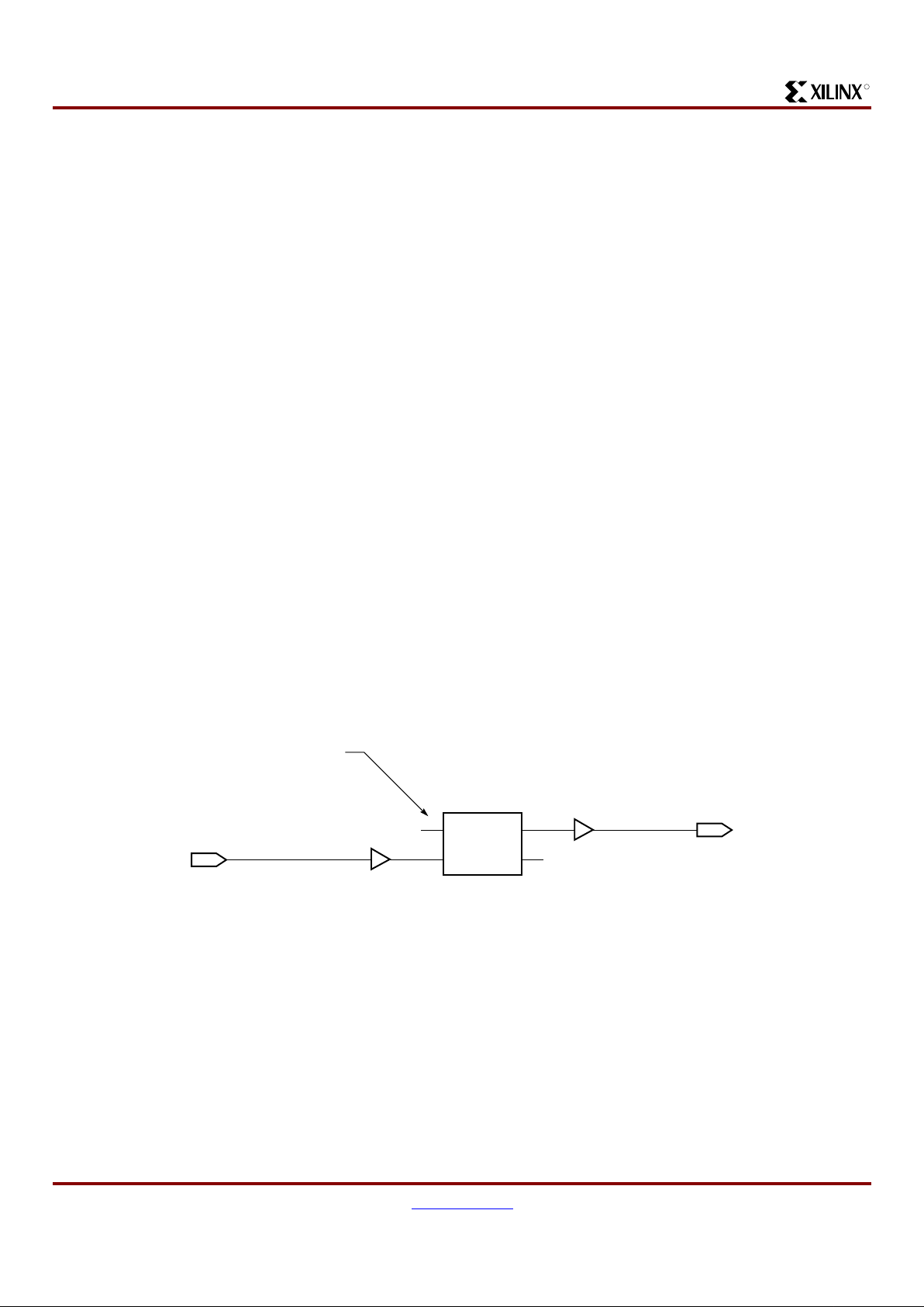
Spartan and Spartan -XL Families Field Programm able Gate Arrays
38 www.xilinx.com DS060 (v1.6) September 19, 2001
1-800-255-7778 Product Speci fication
R
Readback
The user can read back the content of configuration memory and the level of certain internal nodes without interfering
with the normal operation of the device.
Readback not only reports the downloaded configuration
bits, but can also include the present state of the device,
represented by the content of all flip-flops and latches in
CLBs and IOBs, as well as the content of function generators used as RAMs.
Although readback can be performed while the device is
operating, for best results and to freeze a known capture
state, it is recommended that the clock inputs be stopped
until readback is complete.
Readback of Spartan-XL Express mode bitstreams results
in data that does not resemble the original bitstream,
because the bitstream format differs from other modes.
Spartan/XL Readback does not use any dedicated pins, but
uses four internal nets (RDBK.TRIG, RDBK.DATA,
RDBK.RIP and RD BK.CLK ) that can be routed to any IOB.
To access the internal Readback signals, instantiate the
READBACK library symbol and attach the a ppropr iate pad
symbols, as shown in Figure 32.
After Readback has been initiated by a Low-to-High transition on RDBK.TRIG, the RDBK.RIP (Read In Progress) output goes High on the next rising edge of RDBK.CLK.
Subsequent rising e dges of this clock shift out Readback
data on the RDBK.DATA net.
Readback data does not include the preamble, but starts
with five dummy bits ( all High) f ollo wed by the St art bit (Low)
of the first frame. The first two data bits of the first frame are
always High.
Each frame ends with four error check bits. They are read
back as High. The last seven bits of the last frame are also
read back as High. An additional Start bit (Low) and an
11-bit Cyclic Redundancy Check (CRC) signature follow,
before RDBK.RIP returns Low.
Readback Options
Readback options are: Readback Capture, Readback
Abort, and Clock Select. They are set with the bitstream
generation software.
Readback Capture
When the Readback Capture op tion is selected, the data
stream includes sampled values of CLB and IOB signals.
The rising edge of RDB K.TRIG latches the inverted values
of the four CLB outputs, the IOB output flip-flops and the
input signals I1 and I2. Note that while the bits describing
configuration (interconnect, function generators, and RAM
content) are not inverted, the CLB and IOB outp ut signals
are inverted. RDB K.TR IG is locat ed i n the l ower-left cor ner
of the device.
When the Readback Capture option is not selected, the values of the capture bits reflect the configuration data originally written to those memory locations. If the RAM
capabilit y of the CLBs is used, RAM data are available in
Readback, since they directly overwrite the F and G f unction-table configuration of the CLB.
Figure 32: Readback Schematic Example
READBACK
DATA
RIP
TRIG
CLK
READ_DATA
OBUF
READ_TRIGGER
IBUF
DS060_31_080400
If Unconnected,
Default is CCLK

Spartan and Spartan -XL Families Field Programmabl e Gate Arrays
DS060 (v1.6) September 19, 2001 www.xilinx.com 39
Product Speci fication 1-800-255-7778
R
Readback Abort
When the Readback Abort option is selected, a High-to-Low
transition on RDBK.TRIG ter minates the Re adback operation and prepares the logic to accept another trigger.
After an aborted Readback, additional clocks (up to one
Readback clock per configuration frame) may be required to
re-initialize the control logic. The status of Readback is indicated by the output control net RDBK.RIP. RDBK.RIP is
High whenever a readback is in progress.
Clock Select
CCLK is the default clock. However, the user can insert
another clock on R DBK.CLK. Readback con trol and da ta
are clocked on rising edges of RDBK.CLK. If Readback
must be inhibited for security reasons, the Readback control
nets are simply not connected. RDBK.CLK is located in the
lower right chip corner.
Violating the Maximum High and Low Time
Specification for the Readback Clock
The Readback clock has a maximum Hig h and Low time
specification. In some cases, this specification cannot be
met. For example, if a processor is controlling Readback, an
interrupt may force it to stop in the middle of a readback.
This necessitates stop ping the clock, and thus violating the
specification.
The specification is mandatory only on clocking data at the
end of a frame prior to the next start bit. The transfer mechanism will load the data to a shift register during the last six
clock cycles of the frame, prior to the start bit of the following
frame. This loading process is dynamic, and is the source of
the maximum High and Low time requirements.
Therefore, the specification only applies to the six clock
cycles prior to and including any start bit, including the
clocks before the first start bit in the Readback data stream.
At other times, the frame data is already in the reg ister and
the register is not dynamic. Thus, it can be shifted out just
like a regular shift register.
The user must precisely calculat e the locat ion of the R eadback data relative to the frame. The system must keep track
of the position within a data frame, and disable interrupts
before frame boundaries. Frame lengths and data formats
are listed in Table 16 and Table 17.

Spartan and Spartan -XL Families Field Programm able Gate Arrays
40 www.xilinx.com DS060 (v1.6) September 19, 2001
1-800-255-7778 Product Speci fication
R
Readback Switching Charateristics Guidelines
The following guidelines reflect worst-case values ove r the
recommended operating conditions.
Figure 33: Spartan and Spartan-XL Readback Timing Diagram
Spartan and Spar tan-XL Read back Switching Characteristi cs
Symbol Description Min Max Units
T
RTRC
rdbk.TRIG rdbk.TRIG setup to initiate and abort Readback 200 - ns
T
RCRT
rdbk.TRIG hold to initiate and abort Readback 50 - ns
T
RCRD
rdclk.I rdbk.DATA delay - 250 ns
T
RCRR
rdbk.RIP delay - 250 ns
T
RCH
High time 250 500 ns
T
RCL
Low time 250 500 ns
Notes:
1. Timing parameters apply t o all speed grades.
2. If rdbk.TRIG is High prior to Finished, Finished will trigger the first Readback.
T
RTRC
T
RCRT
T
RCH
T
RCRR
T
RCRD
T
RTRC
T
RCRT
T
RCL
DUMMY DUMMY
rdbk.DATA
rdbk.RIP
rdclk.I
rdbk.TRIG
Finished
Internal Net
VALID
DS060_32_080400
VALID

Spartan and Spartan -XL Families Field Programmabl e Gate Arrays
DS060 (v1.6) September 19, 2001 www.xilinx.com 41
Product Speci fication 1-800-255-7778
R
Configuration Switching Characteristics
Master Mode
Slave Mode
DS060_33_080400
T
POR
V
CC
PROGRAM
Mode Pins
(Required)
CCLK Output or Input
DONE Response
RE-PROGRAM
I/O
INIT
T
PI
T
CCLK
T
ICCK
>300 ns
<300 ns
<300 ns
Symbol Description Min Max Units
T
POR
Power-on reset 40 130 ms
T
PI
Program Latency 30 200 µs per CLB column
T
ICCK
CCLK (output) delay 40 250 µs
T
CCLK
CCLK (output) period, slow 640 2000 ns
T
CCLK
CCLK (output) period, fast 100 250 ns
Symbol Description Min Max Units
T
POR
Power-on reset 10 33 ms
T
PI
Program latency 30 200 µs per CLB column
T
ICCK
CCLK (input) delay (required) 4 - µs
T
CCLK
CCLK (input) period (required) 80 - ns

Spartan and Spartan -XL Families Field Programm able Gate Arrays
42 www.xilinx.com DS060 (v1.6) September 19, 2001
1-800-255-7778 Product Speci fication
R
Spartan Detailed Specifications
Definition of Terms
In the following tables, some specifications may be designated as Advance or Preliminary. These term s are defined as
follows:
Advance: Initial estimates based on simulation and/or extrapolation from other speed grades, devices, or families. Values
are subject to change. Use as estimates, not for production.
Preliminary: Based on preliminary characterization. Further changes are not expected.
Unmarked: Specifications not identified as either Advance or Preliminary are to be considered Final.
Notwithstanding the definition of the above terms, all specifications are subject to change without notice.
Except for pin-to-pin input and output parameters, the AC parameter delay specifications included i n this document are
derived from measuring internal test patterns. All specifications are representative of worst-case supply voltage and junction
temperature conditions. The parameters included are common to popular designs and typical applications.
Spartan Absolute Maximum Ratings
(1)
Spartan Recommended Operating Conditions
Symbol Description Value Units
V
CC
Supply voltage relative to GND –0.5 to +7.0 V
V
IN
Input voltage relative to GND
(2,3)
–0.5 to VCC +0.5 V
V
TS
Voltage applied to 3-state output
(2,3)
–0.5 to VCC +0.5 V
T
STG
Storage temperature (ambient) –65 to +150 °C
T
J
Junction temperature Plastic packages +125 °C
Notes:
1. Stresses beyond those listed under Absolute Maximum Ratings may cause permanent damage to the device. These are stress
ratings only, and fu nctional operat ion of the device at these or any other conditions beyond those list ed under Operating Conditions
is not implied. Exposure to Absolute Maximum Ratings condition s for extended periods of time ma y affect device reliability.
2. Maximum DC over shoot (above V
CC
) or undershoot (below GND) must be limited to either 0.5V or 10 mA, whichever is easier to
achieve.
3. Maximum A C ( during t ransi tio ns) condi tions ar e as follows; the de vice pi ns m ay under shoo t to –2.0V or overshoot to +7.0V, provided
this over shoot or undershoot las ts no more than 11 ns with a forcing cur rent no greater than 100 mA.
4. For soldering guidelines, see the Package Infomation on the Xilinx website.
Symbol Description Min Max Units
V
CC
Supply voltage relative to GND, TJ = 0°C to +85°C Commercial 4.75 5.25 V
Supply voltage relative to GND , T
J
= –40°C to +100°C
(1)
Industrial 4.5 5.5 V
V
IH
High-level input voltage
(2)
TTL inputs 2.0 V
CC
V
CMOS inputs 70% 100% V
CC
V
IL
Low-level input voltag e
(2)
TTL inputs 0 0.8 V
CMOS inputs 0 20% V
CC
T
IN
Input signal transition time - 250 n s
Notes:
1. At junction te mper atures abo ve t hose list ed as Reco mmended O perat ing Cond iti ons , all del a y par amet ers i ncrease b y 0.35% per °C.
2. Input and out put measurement thresholds are: 1.5V for TTL and 2.5V for CMOS.

Spartan and Spartan -XL Families Field Programmabl e Gate Arrays
DS060 (v1.6) September 19, 2001 www.xilinx.com 43
Product Speci fication 1-800-255-7778
R
Spartan DC Characteristics Over Operating Conditions
Spartan Global Buffer Switching Characteristic Gu idelines
Testing of the switching parameters is modeled after testing
methods specified by MIL-M-38510/605. All devices are
100% functionally tested. Internal timing parameters are
derived from measuri ng i nter n al tes t patter ns. Listed below
are representative values where one global clock input
drives one vertical clock line in each accessibl e column, and
where all accessible IOB and CLB flip-flops are cl ocked by
the global clock net.
When fewer vertical clock lines are connected, the clock distribution is faster; when multiple clock lines per column are
driven from the same gl obal clock, the delay is longer. For
more specific, more precise, and worst-case guaranteed
data, reflecting the actual routing struc ture, use the values
provided by the static timing analyzer (TRCE in the Xilinx
Development System) and back-annotated to the simulation
netlist. These path delays, provided as a guideline, have
been extracted from the static timing analyzer report. All
timing parameters assume worst-case operating conditions
(supply voltage and junction temperature).
Symbol Description Min Max Units
V
OH
High-level output voltage @ IOH = –4.0 mA, VCC min TTL outputs 2.4 - V
High-level output voltage @ I
OH
= –1.0 mA, VCC min CMOS outputs VCC – 0.5 - V
V
OL
Low-level output voltage @ IOL = 12.0 mA, VCC min
(1)
TTL outputs - 0.4 V
CMOS outputs - 0.4 V
V
DR
Data retention supply voltage (below which configuration data may be lost) 3.0 - V
I
CCO
Quiescent FPGA supply current
(2)
Commercial - 3.0 mA
Industrial - 6.0 mA
I
L
Input or output leakage current –10 +10 µA
C
IN
Input capacitance (sample tested) - 10 pF
I
RPU
Pad pull-up (when selected) @ VIN = 0V (sample tested) 0.02 0.25 mA
I
RPD
Pad pull-down (when selected) @ VIN = 5V (sample tested) 0.02 - mA
Notes:
1. With 50% of the output s simultaneously si nking 12 mA, up to a maximum of 64 pi ns.
2. With no output current loads , no active input pull- up resistors, all package pins at V
CC
or GND, and the FPGA configured with a Tie
option.
Symbol Description Device
Speed Grade
Units
-4 -3
Max Max
T
PG
From pad through Primary buffer, to any clock K XCS05 2.0 4.0 ns
XCS10 2.4 4.3 ns
XCS20 2.8 5.4 ns
XCS30 3.2 5.8 ns
XCS40 3.5 6.4 ns
T
SG
From pad through Secondary buffer, to any clock K XCS05 2.5 4.4 ns
XCS10 2.9 4.7 ns
XCS20 3.3 5.8 ns
XCS30 3.6 6.2 ns
XCS40 3.9 6.7 ns

Spartan and Spartan -XL Families Field Programm able Gate Arrays
44 www.xilinx.com DS060 (v1.6) September 19, 2001
1-800-255-7778 Product Speci fication
R
Spartan CLB Switching Characteristic Guidelines
Testing of switching parameters is modeled after testing
methods specified by MIL-M-38510/605. All devices are
100% functionally tested. Internal timing parameters are
derived from measuri ng i nter n al tes t patter ns. Listed below
are representative values. For mo re specific, more precise,
and worst-case guaranteed data, use t he values reported
by the static timing analyzer (TRCE in the Xilinx Development System) and back-annotated to the simulation netl ist.
All timing parameters ass ume worst-case operating con ditions (supply voltage and junction temperature). Values
apply to all Spartan devices and expressed in nanoseconds
unless otherwise noted.
Symbol
Description
Speed Grade
Units
-4 -3
Min Max Min Max
Clocks
T
CH
Clock High time 3.0 - 4.0 - ns
T
CL
Clock Low time 3.0 - 4.0 - ns
Combinatorial Delays
T
ILO
F/G inputs to X/Y outputs - 1.2 - 1.6 ns
T
IHO
F/G inputs via H to X/Y outputs - 2.0 - 2.7 ns
T
HH1O
C inputs via H1 via H to X/Y outputs - 1.7 - 2.2 ns
CLB Fast Carry Logic
T
OPCY
Operand inputs (F1, F2, G1, G4) to C
OUT
-1.7-2.1ns
T
ASCY
Add/Subtract input (F3) to C
OUT
-2.8-3.7ns
T
INCY
Initialization inputs (F1, F3) to C
OUT
-1.2-1.4ns
T
SUM
CIN through function generators to X/Y outputs - 2.0 - 2.6 ns
T
BYP
C
IN
to C
OUT
, bypass function generators - 0.5 - 0. 6 ns
Sequential Delays
T
CKO
Clock K to Flip-Flop outputs Q - 2.1 - 2.8 ns
Setup Time before Clock K
T
ICK
F/G inputs 1.8 - 2.4 - ns
T
IHCK
F/G inputs via H 2.9 - 3.9 - ns
T
HH1CK
C inputs via H1 through H 2.3 - 3.3 - ns
T
DICK
C inputs via DIN 1.3 - 2.0 - ns
T
ECCK
C inputs via EC 2.0 - 2.6 - ns
T
RCK
C inputs via S/R, going Low (inactive) 2.5 - 4.0 - ns
Hold Time after Clock K
All Hold tim es, all d evic es 0.0 - 0.0 - ns
Set/Reset Direct
T
RPW
Width (High) 3.0 - 4 .0 - ns
T
RIO
Delay from C inputs via S/R, going High to Q - 3.0 - 4.0 ns
Global Set/Reset
T
MRW
Minimum GSR pulse width 11.5 - 13.5 - ns
T
MRQ
Delay from GSR input to any Q See page 50 for T
RRI
values per device.
F
TOG
Toggle Frequency (MHz)
(for export control purposes)
- 166 - 125 MHz

Spartan and Spartan -XL Families Field Programmabl e Gate Arrays
DS060 (v1.6) September 19, 2001 www.xilinx.com 45
Product Speci fication 1-800-255-7778
R
Spartan CLB RAM Synchronous (Edge-Triggered) Write Operation Guidelines
Testing of switching parameters is modeled after testing
methods specified by MIL-M-38510/605. All devices are
100% functionally tested. Internal timing parameters are
derived from measuri ng i nter n al tes t patter ns. Listed below
are representative values. For mo re specific, more precise,
and worst-case guaranteed data, use t he values reported
by the static timing analyzer (TRCE in the Xilinx Development System) an d back-ann otated to th e simu lation n etlist.
All timing parameters ass ume worst-case operating con ditions (supply voltage and junction temperature). Values
apply to all Spartan devices and are expressed in nanoseconds unless otherwise noted.
Symbol Single Port RAM Size
(1)
Speed Grade
Units
-4 -3
Min Max Min Max
Write Operation
T
WCS
Address write cycle time (clock K period) 16x2 8.0 - 11.6 - ns
T
WCTS
32x1 8.0 - 11.6 - ns
T
WPS
Clock K pulse width (active edge) 16x2 4.0 - 5 .8 - ns
T
WPTS
32x1 4.0 - 5.8 - ns
T
ASS
Address setup time before clock K 16x2 1.5 - 2.0 - ns
T
ASTS
32x1 1.5 - 2.0 - ns
T
AHS
Address hold time after clock K 16x2 0.0 - 0.0 - ns
T
AHTS
32x1 0.0 - 0.0 - ns
T
DSS
DIN setup time before clock K 16x2 1.5 - 2.7 - ns
T
DSTS
32x1 1.5 - 1.7 - ns
T
DHS
DIN hold time after clock K 16x2 0.0 - 0.0 - ns
T
DHTS
32x1 0.0 - 0.0 - ns
T
WSS
WE setup time before clock K 16x2 1.5 - 1.6 - ns
T
WSTS
32x1 1.5 - 1.6 - ns
T
WHS
WE hold time after clock K 16x2 0.0 - 0.0 - ns
T
WHTS
32x1 0.0 - 0.0 - ns
T
WOS
Data valid after clock K 16x2 - 6.5 - 7.9 ns
T
WOTS
32x1 - 7.0 - 9.3 ns
Read Operation
T
RC
Address read cycle time 16x2 2.6 - 2.6 - ns
T
RCT
32x1 3.8 - 3.8 - ns
T
ILO
Data valid after address change (no Write
Enable)
16x2 - 1.2 - 1.6 ns
T
IHO
32x1 - 2.0 - 2.7 ns
T
ICK
Address setup time before clock K 16x2 1.8 - 2.4 - ns
T
IHCK
32x1 2.9 - 3.9 - ns
Notes:
1. Timing for 16 x 1 RAM option i s identical to 16 x 2 RAM timing.

Spartan and Spartan -XL Families Field Programm able Gate Arrays
46 www.xilinx.com DS060 (v1.6) September 19, 2001
1-800-255-7778 Product Speci fication
R
Spartan CLB RAM Synchronous (Edge-Triggered) Write Operation Guidelines (continued)
Testing of switching parameters is modeled after testing
methods specified by MIL-M-38510/605. All devices are
100% functionally tested. Internal timing parameters are
derived from measuri ng i nter n al tes t patter ns. Listed below
are representative values. For mo re specific, more precise,
and worst-case guaranteed data, use t he values reported
by the static timing analyzer (TRCE in the Xilinx Development System) an d back-ann otated to th e simu lation n etlist.
All timing parameters ass ume worst-case operating con ditions (supply voltage and junction temperature). Values
apply to all Spartan devices and are expressed in nanoseconds unless otherwise noted.
Spartan CLB RAM Synchronous (Edge-Triggered) Write Timing
Dual-Port RAM Synchronous (Edge-Triggered) Write Operation Characteristics
Symbol Dual Port RAM Size
(1)
-4 -3
UnitsMin Max Min Max
Write Operation
T
WCDS
Address write cycle time (clock K period) 16x1 8.0 - 11.6 - ns
T
WPDS
Clock K pulse width (active edge) 16x1 4.0 - 5.8 - ns
T
ASDS
Address setup time before clock K 16x1 1.5 - 2.1 - ns
T
AHDS
Address hold time after clock K 16x1 0 - 0 - ns
T
DSDS
DIN setup time before clock K 16x1 1.5 - 1.6 - ns
T
DHDS
DIN hold time after clock K 16x1 0 - 0 - ns
T
WSDS
WE setup time before clock K 16x1 1.5 - 1.6 - n s
T
WHDS
WE hold time after clock K 16x1 0 - 0 - ns
T
WODS
Data valid after clock K 16x1 - 6.5 - 7.0 ns
Notes:
1. Read Operation tim ing for 16 x 1 dual-port RAM option is identical to 16 x 2 single-port RAM timing
Single Port Dual Port
WCLK (K)
WE
ADDRESS
DATA IN
DATA OUT
OLD NEW
T
DSS
T
DHS
T
ASS
T
AHS
T
WSS
T
WPS
T
WHS
T
WSDS
T
WHDS
T
WOS
T
ILO
T
ILO
DS060_34_011300
WCLK (K)
WE
ADDRESS
DATA IN
DATA OUT
OLD NEW
T
DSDS
T
DHDS
T
ASDS
T
AHDS
T
WPDS
T
WODS
T
ILO
T
ILO

Spartan and Spartan -XL Families Field Programmabl e Gate Arrays
DS060 (v1.6) September 19, 2001 www.xilinx.com 47
Product Speci fication 1-800-255-7778
R
Spartan Pin-to-Pin Output Parameter Guidelines
Testing of switching parameters is modeled after testing
methods specified by MIL-M-38510/605. All devices are
100% functionally tested. Pin-to-pin timing parameters are
derived from measuring external and inter nal test patterns
and are guaranteed over worst-case operating conditions
(supply voltage and junction temperature). Listed below are
representative values for typical pin locations and nor mal
clock loading. For more specific, more precise, and
worst-case guaranteed data, reflecting the actual routing
structure, use the values provided by the static timing analyzer (TRCE in the Xilinx Development System) and
back-annotated to the simulation netlist. These path delays,
provided as a guideline, have been extracted from the static
timing analyzer report.
Spartan Output Flip-Flop, Clock-to-Out
Symbol
Description Device
Speed Grade
Units
-4 -3
Max Max
Global Primary Clock to TTL Output using OFF
T
ICKOF
Fast XCS05 5.3 8.7 ns
XCS10 5.7 9.1 ns
XCS20 6.1 9.3 ns
XCS30 6.5 9.4 ns
XCS40 6.8 10.2 ns
T
ICKO
Slew-rate limit e d XCS05 9.0 1 1. 5 ns
XCS10 9.4 12.0 ns
XCS20 9.8 12.2 ns
XCS30 10.2 12.8 ns
XCS40 10.5 12.8 ns
Global Secondary Clock to TTL Output using OFF
T
ICKSOF
Fast XCS05 5.8 9.2 ns
XCS10 6.2 9.6 ns
XCS20 6.6 9.8 ns
XCS30 7.0 9.9 ns
XCS40 7.3 10.7 ns
T
ICKSO
Slew-rate limit e d XCS05 9.5 1 2. 0 ns
XCS10 9.9 12.5 ns
XCS20 10.3 12.7 ns
XCS30 10.7 13.2 ns
XCS40 11.0 14.3 ns
Delay Adder for CMOS Outputs Option
T
CMOSOF
Fast All devices 0.8 1.0 ns
T
CMOSO
Slew-rate limit e d All devices 1.5 2.0 ns
Notes:
1. Listed above are representative val ues where one global clock input drives one vertical clock line in each accessible column,and
where all accessible IOB and CLB flip-flops are clocked b y the global clock net.
2. Output timing is measured at ~50% V
CC
threshold with 50 pF external capacitive load. For di fferent loads, see Figure 33.
3. OFF = Output Flip-Flop

Spartan and Spartan -XL Families Field Programm able Gate Arrays
48 www.xilinx.com DS060 (v1.6) September 19, 2001
1-800-255-7778 Product Speci fication
R
Capacitive Load Factor
Figure 33 shows the relationship between I/O output delay
and load capacitance. It allows a user to adjust the specified
output delay if the load capacitance is differen t than 50 pF.
For example, if the actual load capacitance is 120 pF, add
2.5 ns to the specified delay. If the load capacitance is 20
pF, subtract 0.8 ns from the specified output delay.
Figure 33 is usable over the specified operating conditions
of voltage and temperature and is independent of the output
slew rate control.
Figure 34: Delay Factor at Various Capaci tive Loads
DS060_35_080400
-2
0 20406080
Capacitance (pF)
Delta Delay (ns)
100 120 140
-1
0
1
2
3

Spartan and Spartan -XL Families Field Programmabl e Gate Arrays
DS060 (v1.6) September 19, 2001 www.xilinx.com 49
Product Speci fication 1-800-255-7778
R
Spartan Pin-to-Pin Input Parameter Guidelines
Testing of switching parameters is modeled after testing
methods specified by MIL-M-38510/605. All devices are
100% functionally tested. Pin-to-pin timing parameters are
derived from measuring external and inter nal test patterns
and are guaranteed over worst-case operating conditions
(supply voltage and junction temperature). Listed below are
representative values for typical pin locations and normal
clock loading.
Spartan Primary and Secondary Setup and Hold
Symbol Description Device
Speed Grade
Units
-4 -3
Min Min
Input Setup/Hold Times Using Pr imary Clock and IFF
T
PSUF/TPHF
No Delay XCS05 1.2 / 1.7 1.8 / 2.5 ns
XCS10 1.0 / 2.3 1.5 / 3.4 ns
XCS20 0.8 / 2.7 1.2 / 4.0 ns
XCS30 0.6 / 3.0 0.9 / 4.5 ns
XCS40 0.4 / 3.5 0.6 / 5.2 ns
T
PSU/TPH
With Delay XCS05 4.3 / 0.0 6.0 / 0.0 ns
XCS10 4.3 / 0.0 6.0 / 0.0 ns
XCS20 4.3 / 0.0 6.0 / 0.0 ns
XCS30 4.3 / 0.0 6.0 / 0.0 ns
XCS40 5.3 / 0.0 6.8 / 0.0 ns
Input Setup/Hold Times Using Secondary Clock and IFF
T
SSUF/TSHF
No Delay XCS05 0.9 / 2.2 1.5 / 3.0 ns
XCS10 0.7 / 2.8 1.2 / 3.9 ns
XCS20 0.5 / 3.2 0.9 / 4.5 ns
XCS30 0.3 / 3.5 0.6 / 5.0 ns
XCS40 0.1 / 4.0 0.3 / 5.7 ns
T
SSU/TSH
With Delay XCS05 4.0 / 0.0 5.7 / 0.0 ns
XCS10 4.0 / 0.0 5.7 / 0.0 ns
XCS20 4.0 / 0.5 5.7 / 0.5 ns
XCS30 4.0 / 0.5 5.7 / 0.5 ns
XCS40 5.0 / 0.0 6.5 / 0.0 ns
Notes:
1. Setup time is measured wit h the fastest route and the lightest load. Hold time is measured using the furthest distance and a
referenc e load of one clock pin per IOB/CLB.
2. IFF = Input Flip-flop or Lat ch

Spartan and Spartan -XL Families Field Programm able Gate Arrays
50 www.xilinx.com DS060 (v1.6) September 19, 2001
1-800-255-7778 Product Speci fication
R
Spartan IOB Input Switching Characteristic Guidelines
Testing of switching parameters is modeled after testing
methods specified by MIL-M-38510/605. All devices are
100% functionally tested. Internal timing parameters are
derived from measuri ng i nter n al tes t patter ns. Listed below
are representative values. For mo re specific, more precise,
and worst-case guaranteed data, use t he values reported
by the static timing analyzer (TRCE in the Xilinx Development System) an d back-ann otated to th e simu lation n etlist.
These path delays, provided as a guideline, have been
extracted from the static timing analyzer report. All timing
parameters assume worst-case operating conditions (supply voltage and junction temperature).
Symbol Description Device
Speed Grade
Units
-4 -3
Min Max Min Max
Setup Times - TTL Inputs
(1)
T
ECIK
Clock Enable (EC) to Clock (IK), no delay All devices 1.6 - 2.1 - ns
T
PICK
Pad to Clock (IK), no delay All devices 1.5 - 2.0 - ns
Hold Times
T
IKEC
Clock Enable (EC) to Clock (IK), no delay All devices 0.0 - 0.9 - ns
All Other Ho ld Times All devices 0 . 0 - 0.0 - ns
Propagation Delays - TTL Inputs
(1)
T
PID
Pad to I1, I2 All devices - 1.5 - 2.0 ns
T
PLI
Pad to I1, I2 via transparent input latch, no delay All devices - 2.8 - 3.6 ns
T
IKRI
Clock (IK) to I1, I2 (f l ip -flop ) All devi ces - 2.7 - 2.8 ns
T
IKLI
Clock (IK) to I1, I2 (latch enable, active Low) All devices - 3.2 - 3.9 ns
Delay Adder for Input with Delay Option
T
Delay
T
ECIKD
= T
ECIK
+ T
Delay
T
PICKD
= T
PICK
+ T
Delay
T
PDLI
= T
PLI
+ T
Delay
XCS05 3.6 - 4.0 - ns
XCS10 3.7 - 4.1 - ns
XCS20 3.8 - 4.2 - ns
XCS30 4.5 - 5.0 - ns
XCS40 5.5 - 5.5 - ns
Global Set/Reset
T
MRW
Minimum GSR pulse width All devices 11.5 - 13. 5 - ns
T
RRI
Delay from GSR input to any Q XCS05 - 9.0 - 11.3 ns
XCS10 - 9.5 - 11.9 ns
XCS20 - 10.0 - 12.5 ns
XCS30 - 10.5 - 13.1 ns
XCS40 - 11.0 - 13.8 ns
Notes:
1. Delay adder f or CMOS Inputs option: f or -3 speed grade, add 0.4 ns; for -4 speed grade, add 0.2 ns.
2. Input pad set up and hol d t imes ar e spe cified wi th re spec t to t he int ernal cloc k ( IK). F or set up and ho ld times wi th re spect t o the c lock
input, see the pin-t o-pin parameters in the Pin -to-Pin Input Parameters table.
3. Voltage levels of unused pads, bonded or unbonded, must be valid logic levels. Each can be configured with the internal pull-up
(default) or pull-down resistor, or configured as a driv en output, or can be driven from an external source.

Spartan and Spartan -XL Families Field Programmabl e Gate Arrays
DS060 (v1.6) September 19, 2001 www.xilinx.com 51
Product Speci fication 1-800-255-7778
R
Spartan IOB Output Switching Characteristic Guidelines
Testing of switching parameters is modeled after testing
methods specified by MIL-M-38510/605. All devices are
100% functionally tested. Internal timing parameters are
derived from measuri ng i nter n al tes t patter ns. Listed below
are representative values. For mo re specific, more precise,
and worst-case guaranteed data, use t he values reported
by the static ti ming analyzer (TR CE in the Xilinx Develop-
ment System) an d back-ann otated to th e simu lation n etlist.
These path delays, provided as a guideline, have been
extracted from the static timing analyzer report. All timing
parameters assume worst-case operating conditions (supply voltage and junction temperature). Values are
expressed in nanoseconds unless otherwise noted.
Symbol Description Device
Speed Grade
Units
-4 -3
Min Max Min Max
Clocks
T
CH
Clock High All devices 3.0 - 4.0 - ns
T
CL
Clock Low All devices 3.0 - 4. 0 - ns
Propagation Delays - TTL Outputs
(1,2)
T
OKPOF
Clock (OK) to Pad, fast All devices - 3.3 - 4.5 ns
T
OKPOS
Clock (OK to Pad, s lew-rate limited All devices - 6.9 - 7.0 n s
T
OPF
Output (O) to Pad, fast All devices - 3.6 - 4.8 ns
T
OPS
Output (O) to Pad, slew-rate limited All devices - 7.2 - 7.3 ns
T
TSHZ
3-state to Pad High-Z (slew-rate independent) All devices - 3.0 - 3.8 ns
T
TSONF
3-state to Pad active and valid, fast All devices - 6.0 - 7.3 ns
T
TSONS
3-state to Pad active and valid, slew-rate limited All devices - 9.6 - 9.8 ns
Setup and Hold Times
T
OOK
Output (O) to cloc k ( O K) set u p time All devices 2.5 - 3.8 - ns
T
OKO
Output (O) to clock (OK) hold time All de vices 0.0 - 0.0 - ns
T
ECOK
Clock Enab l e (EC) to clock (OK) setup time All devices 2.0 - 2.7 - ns
T
OKEC
Clock Enable (EC) to clock (OK) hold time All devices 0. 0 - 0.5 - ns
Global Set/Reset
T
MRW
Minimum GSR pulse width All devices 11.5 13.5 ns
T
RPO
Delay from GSR input to any Pad XCS05 - 12.0 - 15.0 ns
XCS10 - 12.5 - 15.7 ns
XCS20 - 13.0 - 16.2 ns
XCS30 - 13.5 - 16.9 ns
XCS40 - 14.0 - 17.5 ns
Notes:
1. Delay adder for CMOS Outputs option (with fast slew rate option): for -3 speed grade, add 1.0 ns; for -4 speed grade, add 0.8 ns.
2. Delay adder for CMOS Outputs option (with slow slew rate option): for -3 speed grade, add 2.0 ns; for -4 speed grade, add 1.5ns.
3. Output timing is measured at ~50% V
CC
threshold, wit h 50 pF e xternal ca pacitiv e loads i ncludi ng tes t fi xture . Sl e w-rat e li mited out put
rise/fall times are approximately two time s longer than fast out put rise/fall times.
4. Voltage levels of unused pads, bonded or unbonded, must be valid logic levels. Each can be configured with the internal pull-up
(default) or pull-down resistor, or configured as a driv en output, or can be driven from an external source.

Spartan and Spartan -XL Families Field Programm able Gate Arrays
52 www.xilinx.com DS060 (v1.6) September 19, 2001
1-800-255-7778 Product Speci fication
R
Spartan-XL Detaile d Specifications
Definition of Terms
In the following tables, some specifications may be designated as Advance or Preliminary. These term s are defined as
follows:
Advance: Initial estimates based on simulation and/or extrapolation from ot her speed gra des, devices, or device families.
Values are subject to change. Use as estimates, not for production.
Preliminary: Based on preliminary characterization. Further changes are not expected.
Unmarked: Specifications not identified as either Advance or Preliminary are to be considered Final.
Notwithstanding the definition of the above terms, all specifications are subject to change without notice.
Except for pin-to-pin input and output parameters, the AC parameter delay specifications included i n this document are
derived from measuring internal test patterns. All specifications are representative of worst-case supply voltage and junction
temperature conditions. The parameters included are common to popular designs and typical applications.
Spartan-XL Absolute Maximum Ratings
(1)
Spartan-XL Recommended Oper ating Conditions
Symbol Description Value Units
V
CC
Supply voltage relative to GND –0.5 to 4.0 V
V
IN
Input voltage relative to GND 5V Tolerant I/O Checked
(2, 3)
–0.5 to 5.5 V
Not 5V To lerant I/Os
(4, 5)
–0.5 to VCC + 0.5 V
V
TS
Voltage applied to 3-state output 5V Tolerant I/O Checked
(2, 3)
–0.5 to 5.5 V
Not 5V To lerant I/Os
(4, 5)
–0.5 to VCC + 0.5 V
T
STG
Storage temperature (ambient) –65 to +150 °C
T
J
Junction temperature Plastic packages +125 °C
Notes:
1. Stresses beyond those listed under Absolute Maximum Ratings may cause permanent damage to the device. These are stress
ratings only, and fu nctional operat ion of the device at these or any other conditions beyond those list ed under Operating Conditions
is not implied. Exposure to Absolute Maximum Ratings condition s for extended periods of time ma y affect device reliability.
2. With 5V Tolerant I/ Os selected, the Maximum DC overshoot must be limited t o either +5.5V or 10 mA and under shoot (below GND)
must be limited to ei ther 0.5V or 10 mA, whichever is easier to achieve.
3. With 5V Tolerant I/Os selected, the Maximum AC (during transitions) conditions are as follows; the device pins may under shoot to
–2.0V or ov ershoot to + 7.0V, provided this overshoot or undershoot lasts no more than 11 ns with a f orcing current no greater t han
100 mA.
4. Without 5V Tolerant I /Os selected, the Maximum DC overshoot or undershoot m ust be limited to either 0.5V or 10 mA, whichever is
easier to achieve.
5. Without 5V Tolerant I/Os sel ected, the Max imum AC con ditions are as f ollo ws; the de vice pin s may undersho ot to –2.0V or overshoot
to V
CC
+ 2.0V, provided this ov ershoot or undershoot lasts no more than 11 ns with a forcing current no greater than 100 mA.
6. For soldering guidelines, see the Package Infomation on the Xilinx website.
Symbol Description Min Max Units
V
CC
Supply voltage relative to GND, TJ = 0°C to +85°C Commercial 3.0 3.6 V
Supply voltage relative to GND , T
J
= –40°C to +100°C
(1)
Industrial 3.0 3.6 V
V
IH
High-level input voltage
(2)
50% of V
CC
5.5 V
V
IL
Low-level input voltag e
(2)
030% of VCCV
T
IN
Input signal transition time - 250 ns
Notes:
1. At junction temperatures above those listed as Operating Conditions, all delay param eters increase by 0.35% per
°C.
2. Input and out put measurement threshold is ~50% of V
CC
.

Spartan and Spartan -XL Families Field Programmabl e Gate Arrays
DS060 (v1.6) September 19, 2001 www.xilinx.com 53
Product Speci fication 1-800-255-7778
R
Spartan-XL DC Characteristics Over Operating Conditions
Supply Current Requirements During Power-On
Spartan-XL F PGAs require that a minimum supply current
I
CCPO
be provided to the VCC lines for a successful power
on. If more current is available, the FPGA can consume
more than I
CCPO
min., though this cannot adversely affect
reliability.
A maximum limit for I
CCPO
is not specified. Be careful when
using foldback/crowbar supplies and fuses. It is possible to
control the magnitude of I
CCPO
by limiting the supply current
available to the FPGA. A current limit below the trip level will
avoid inadvertently activating over-current protection circuits.
Symbol Description Min Typ. Max Units
V
OH
High-level output voltage @ IOH = –4.0 mA, VCC min (LVTTL) 2.4 - - V
High-level output voltage @ I
OH
= –500 µA, (LVC MOS) 90% V
CC
--V
V
OL
Low-level output voltage @ IOL = 12.0 mA, VCC min (LVTTL)
(1)
--0.4V
Low-level output voltage @ I
OL
= 24.0 mA, VCC min (LVTTL)
(2)
--0.4V
Low-level output voltage @ I
OL
= 1500 µA, (LVCMOS) - - 10% V
CC
V
V
DR
Data retention supply voltage (below which configuration data
may be lost)
2.5 - - V
I
CCO
Quiescent FPGA supply current
(3,4)
Commercial - 0.1 2.5 mA
Industrial - 0.1 5 mA
I
CCPD
Power Down FPGA supply current
(3,5)
Commercial - 0.1 2.5 mA
Industrial - 0.1 5 mA
I
L
Input or output leakage current –10 - 10 µA
C
IN
Input capacitance (sample tested) - - 10 pF
I
RPU
Pad pull-up (when selected) @ VIN = 0V (sample tested) 0.02 - 0.25 mA
I
RPD
Pad pull-down (when selected) @ VIN = 3.3V (sample tested) 0. 02 - - mA
Notes:
1. With up to 64 pins simultaneously sinking 12 mA (default mode).
2. With up to 64 pins simultaneously sinking 24 mA (with 24 mA option selected).
3. With 5V tolerance not sel ected, no internal oscillators, and the FPGA con fi gured with the Tie option.
4. With no output current loads, no activ e input resistors, and all package pins at V
CC
or GND.
5. With PWRDWN
active.
Symbol Description Min Max Units
I
CCPO
Total VCC supply current required during power-on 100 - mA
T
CCPO
VCC ramp ti me
(2,3)
-50ms
Notes:
1. The I
CCPO
requirement applies for a brief time (commonly only a few milliseconds) when VCC ramps from 0 to 3.3V.
2. The ramp time is measured from GND to V
CC
max on a fully loaded board.
3. V
CC
must not dip in the negative direction during power on.
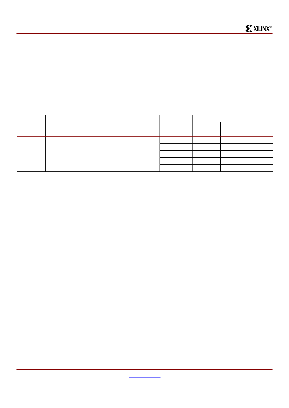
Spartan and Spartan -XL Families Field Programm able Gate Arrays
54 www.xilinx.com DS060 (v1.6) September 19, 2001
1-800-255-7778 Product Speci fication
R
Spartan-XL Global Buffer Switching Characteristic Guidelines
Testing of the switching parameters is modeled after testing
methods specified by MIL-M-38510/605. All devices are
100% functionally tested. Internal timing parameters are
derived from measuri ng i nter n al tes t patter ns. Listed below
are representative values where one global clock input
drives one vertical clock line in each accessibl e column, and
where all accessible IOB and CLB flip-flops are cl ocked by
the global clock net.
When fewer vertical clock lines are connected, the clock distribution is faster; when multiple clock lines per column are
driven from the same gl obal clock, the delay is longer. For
more specific, more precise, and worst-case guaranteed
data, reflecting the actual routing struc ture, use the values
provided by the static timing analyzer (TRCE in the Xilinx
Development System) and back-annotated to the simulation
netlist. These path delays, provided as a guideline, have
been extracted from the static timing analyzer report. All
timing parameters assume worst-case operating conditions
(supply voltage and junction temperature).
Symbol Description Device
Speed Grade
Units
-5 -4
Max Max
T
GLS
From pad through buffer, to any clock K X CS 05XL 1.4 1.5 ns
XCS10XL 1.7 1.8 ns
XCS20XL 2.0 2.1 ns
XCS30XL 2.3 2.5 ns
XCS40XL 2.6 2.8 ns

Spartan and Spartan -XL Families Field Programmabl e Gate Arrays
DS060 (v1.6) September 19, 2001 www.xilinx.com 55
Product Speci fication 1-800-255-7778
R
Spartan-XL CLB Switching Characteristic Guidelines
Testing of switching parameters is modeled after testing
methods specified by MIL-M-38510/605. All devices are
100% functionally tested. Internal timing parameters are
derived from measuri ng i nter n al tes t patter ns. Listed below
are representative values. For mo re specific, more precise,
and worst-case guaranteed data, use t he values reported
by the static timing analyzer (TRCE in the Xilinx Development System) and back-annotated to the simulation netl ist.
All timing parameters ass ume worst-case operating con ditions (supply voltage and junction temperature). Values
apply to all Spar tan-XL devices and expressed in nanoseconds unless otherwise noted.
Symbol Description
Speed Grade
Units
-5 -4
Min M ax Min Max
Clocks
T
CH
Clock High time 2.0 - 2.3 - ns
T
CL
Clock Low time 2.0 - 2.3 - ns
Combinatorial Delays
T
ILO
F/G inputs to X/Y outputs - 1.0 - 1.1 ns
T
IHO
F/G inputs via H to X/Y outputs - 1.7 - 2.0 ns
T
ITO
F/G inputs via transparent latch to Q outputs - 1.5 - 1.8 ns
T
HH1O
C inputs via H1 via H to X/Y outputs - 1.5 - 1.8 ns
Sequential Delays
T
CKO
Clock K to Flip-Flop or latch outputs Q - 1.2 - 1.4 ns
Setup Time before Clock K
T
ICK
F/G inputs 0.6 - 0.7 - ns
T
IHCK
F/G inputs via H 1.3 - 1.6 - ns
Hold Time after Clock K
All Hold times, all d evic es 0.0 - 0 .0 - ns
Set/Reset Direct
T
RPW
Width (High) 2.5 - 2.8 - ns
T
RIO
Delay from C inputs via S/R, going High to Q - 2.3 - 2.7 ns
Global Set/Reset
T
MRW
Minimum GSR Pulse Width 10.5 - 11.5 - ns
T
MRQ
Delay from GSR input to any Q See page 60 for T
RRI
values per device.
F
TOG
Toggle Frequency (MHz)
(for export control purposes)
-250-217MHz

Spartan and Spartan -XL Families Field Programm able Gate Arrays
56 www.xilinx.com DS060 (v1.6) September 19, 2001
1-800-255-7778 Product Speci fication
R
Spartan-XL CLB RAM Synchronous (Edge-Triggered) Write Operation Guidelines
Testing of switching parameters is modeled after testing
methods specified by MIL-M-38510/605. All devices are
100% functionally tested. Internal timing parameters are
derived from measuri ng i nter n al tes t patter ns. Listed below
are representative values. For mo re specific, more precise,
and worst-case guaranteed data, use t he values reported
by the static timing analyzer (TRCE in the Xilinx Development System) an d back-ann otated to th e simu lation n etlist.
All timing parameters ass ume worst-case operating con ditions (supply voltage and junction temperature). Values
apply to all Spartan-XL devices and are expressed in nanoseconds unless otherwise noted.
Symbol Single Port RAM Size
(1)
Speed Grade
Units
-5 -4
Min Max Min Max
Write Operation
T
WCS
Address write cycle time (clock K period) 16x2 7.7 - 8.4 - ns
T
WCTS
32x1 7.7 - 8.4 - ns
T
WPS
Clock K pulse width (active edge) 16x2 3.1 - 3.6 - ns
T
WPTS
32x1 3.1 - 3.6 - ns
T
ASS
Address setu p t ime bef ore cloc k K 16x2 1. 3 - 1.5 - ns
T
ASTS
32x1 1.5 - 1.7 - ns
T
DSS
DIN setup time before clock K 16x2 1.5 - 1.7 - ns
T
DSTS
32x1 1.8 - 2.1 - ns
T
WSS
WE setup time before clock K 16x2 1.4 - 1.6 - ns
T
WSTS
32x1 1.3 - 1.5 - ns
All hold times after clock K 16x2 0.0 - 0.0 - ns
T
WOS
Data valid after clock K 32x1 - 4.5 - 5.3 ns
T
WOTS
16x2 - 5.4 - 6.3 ns
Read Operation
T
RC
Address read cycle time 16x 2 2.6 - 3.1 - ns
T
RCT
32x1 3.8 - 5.5 - ns
T
ILO
Data Valid after address change (no Write
Enable)
16x2 - 1.0 - 1.1 ns
T
IHO
32x1 - 1.7 - 2.0 ns
T
ICK
Address setu p t ime bef ore cloc k K 16x2 0. 6 - 0.7 - ns
T
IHCK
32x1 1.3 - 1.6 - ns
Notes:
1. Timing for 16 x 1 RAM option i s identical to 16 x 2 RAM timing.

Spartan and Spartan -XL Families Field Programmabl e Gate Arrays
DS060 (v1.6) September 19, 2001 www.xilinx.com 57
Product Speci fication 1-800-255-7778
R
Spartan-XL CLB RAM Synchronous (Edge-Triggered) Write Operation Guidelines (cont.)
Testing of switching parameters is modeled after testing
methods specified by MIL-M-38510/605. All devices are
100% functionally tested. Internal timing parameters are
derived from measuri ng i nter n al tes t patter ns. Listed below
are representative values. For mo re specific, more precise,
and worst-case guaranteed data, use t he values reported
by the static timing analyzer (TRCE in the Xilinx Development System) an d back-ann otated to th e simu lation n etlist.
All timing parameters ass ume worst-case operating con ditions (supply voltage and junction temperature). Values
apply to all Spartan-XL devices and are expressed in nanoseconds unless otherwise noted.
Spartan-XL CLB RAM Synchronous (Edge-Triggered) Write Timing
Symbol Dual Port RAM Size
-5 -4
UnitsMin Max Min Max
Write Operation
(1)
T
WCDS
Address write cycle time (clock K period) 16x1 7.7 - 8.4 - ns
T
WPDS
Clock K pulse width (active edge) 16x1 3.1 - 3.6 - ns
T
ASDS
Address setup time before clock K 16x1 1.3 - 1.5 - ns
T
DSDS
DIN setup time before clock K 16x1 1.7 - 2.0 - ns
T
WSDS
WE setup time before clock K 16x1 1.4 - 1.6 - n s
All hold times after clock K 16x1 0 - 0 - ns
T
WODS
Data valid after clock K 16x1 - 5.2 - 6.1 ns
Notes:
1. Read Operation tim ing for 16 x 1 dual-port RAM option is identical to 16 x 2 single-port RAM timing
Single Port Dual Port
WCLK (K)
WE
ADDRESS
DATA IN
DATA OUT
OLD NEW
T
DSS
T
DHS
T
ASS
T
AHS
T
WSS
T
WPS
T
WHS
T
WSDS
T
WHDS
T
WOS
T
ILO
T
ILO
DS060_34_011300
WCLK (K)
WE
ADDRESS
DATA IN
DATA OUT
OLD NEW
T
DSDS
T
DHDS
T
ASDS
T
AHDS
T
WPDS
T
WODS
T
ILO
T
ILO

Spartan and Spartan -XL Families Field Programm able Gate Arrays
58 www.xilinx.com DS060 (v1.6) September 19, 2001
1-800-255-7778 Product Speci fication
R
Spartan-XL Pin-to-Pin Output Parameter Guidelines
Testing of switching parameters is modeled after testing
methods specified by MIL-M-38510/605. All devices are
100% functionally tested. Pin-to-pin timing parameters are
derived from measuring external and inter nal test patterns
and are guaranteed over worst-case operating conditions
(supply voltage and junction temperature). Listed below are
representative values for typical pin locations and normal
clock loading.
Spartan-XL Output Flip-Flop, Clock-to-Out
Symbol Description Device
Speed Grade
Units
-5 -4
Max Max
Global Clock to Output using OFF
T
ICKOF
Fast XCS05XL 4.6 5.2 ns
XCS10XL 4.9 5.5 ns
XCS20XL 5.2 5.8 ns
XCS30XL 5.5 6.2 ns
XCS40XL 5.8 6.5 ns
Slew Rate Adjustment
T
SLOW
For Output SLOW option add All Devices 1.5 1.7 ns
Notes:
1. Output delays are representative values where one global clock input drives one vertical clock line in each accessible col um n ,and
where all accessible IOB and CLB flip-flops are clocked b y the global clock net.
2. Output timing is measured at ~50% V
CC
threshold with 50 pF external capacitiv e load.
3. OFF = Output Flip Flop
Spartan and Spartan -XL Families Field Programmabl e Gate Arrays
DS060 (v1.6) September 19, 2001 www.xilinx.com 59
Product Speci fication 1-800-255-7778
R
Spartan-XL Pin-to-Pin Input Parameter Guidelines
Testing of switching parameters is modeled after testing
methods specified by MIL-M-38510/605. All devices are
100% functionally tested. Pin-to-pin timing parameters are
derived from measuring external and inter nal test patterns
and are guaranteed over worst-case operating conditions
(supply voltage and junction temperature). Listed below are
representative values for typical pin locations and normal
clock loading.
Spartan-XL Set up and Hold
Capacitive Load Factor
Figure 35 shows the relationship between I/O output delay
and load capacitance. It allows a user to adjust the specified
output delay if the load capacitance is differen t than 50 pF.
For example, if the actual load capacitance is 120 pF, add
2.5 ns to the specified delay. If the load capacitance is 20
pF, subtract 0.8 ns from the specified output delay.
Figure 35 is usable over the specified operating conditions
of voltage and temperature and is independent of the output
slew rate control.
Symbol Description Device
Speed Grade
Units
-5 -4
Max Max
Input Setup/Hold Times Using Global Clock and IFF
T
SUF/THF
No Delay XCS05XL 1.1/2.0 1.6/2.6 ns
XCS10XL 1.0/2.2 1.5/2.8 ns
XCS20XL 0.9/2.4 1.4/3.0 ns
XCS30XL 0.8/2.6 1.3/3.2 ns
XCS40XL 0.7/2.8 1.2/3.4 ns
T
SU/TH
Full Delay XCS05XL 3.9/0.0 5.1/0.0 ns
XCS10XL 4.1/0.0 5.3/0.0 ns
XCS20XL 4.3/0.0 5.5/0.0 ns
XCS30XL 4.5/0.0 5.7/0.0 ns
XCS40XL 4.7/0.0 5.9/0.0 ns
Notes:
1. IFF = Input Flip-Flop or Latch
2. Setup time is measured wit h the fastest route and the lightest load. Hold time is measured using the furthest distance and a
referenc e load of one clock pin per IOB/CLB.
Figure 35: Delay Factor at Various Capaci tive Loads
DS060_35_080400
-2
0 20406080
Capacitance (pF)
Delta Delay (ns)
100 120 140
-1
0
1
2
3

Spartan and Spartan -XL Families Field Programm able Gate Arrays
60 www.xilinx.com DS060 (v1.6) September 19, 2001
1-800-255-7778 Product Speci fication
R
Spartan-XL IOB Input Switch ing Characteristic Guidelines
Testing of switching parameters is modeled after testing
methods specified by MIL-M-38510/605. All devices are
100% functionally tested. Internal timing parameters are
derived from measuri ng i nter n al tes t patter ns. Listed below
are representative values. For mo re specific, more precise,
and worst-case guaranteed data, use t he values reported
by the static timing analyzer (TRCE in the Xilinx Development System) an d back-ann otated to th e simu lation n etlist.
These path delays, provided as a guideline, have been
extracted from the static timing analyzer report. All timing
parameters assume worst-case operating conditions (supply voltage and junction temperature).
Symbol Device
Speed Grade
Units
-5 -4
Description Min Max Min Max
Setup Times
T
ECIK
Clock Enable (EC) to Clock (IK) All devices 0.0 - 0.0 - ns
T
PICK
Pad to Clock (IK), no delay All devices 1.0 - 1.2 - ns
T
POCK
Pad to Fast Capture Latch Enable (OK), no delay All devices 0.7 - 0.8 - ns
Hold Times
All Hold Time s All devices 0. 0 - 0.0 - ns
Propagation Delays
T
PID
Pad to I1, I2 All devi ces - 0.9 - 1.1 ns
T
PLI
Pad to I1, I2 via transparent input latch, no delay All devices - 2.1 - 2.5 ns
T
IKRI
Clock (IK) to I1, I2 (flip-fl o p) All devices - 1.0 - 1.1 ns
T
IKLI
Clock (IK) to I1, I2 (latch enable, active Low) All devices - 1.1 - 1.2 ns
Delay Adder for Input with Full Delay Option
T
Delay
T
PICKD
= T
PICK
+ T
Delay
T
PDLI
= T
PLI
+ T
Delay
XCS05XL 4.0 - 4.7 - ns
XCS10XL 4.8 - 5.6 - ns
XCS20XL 5.0 - 5.9 - ns
XCS30XL 5.5 - 6.5 - ns
XCS40XL 6.5 - 7.6 - ns
Global Set/Reset
T
MRW
Minimum GSR pulse width All devices 10.5 - 11.5 - ns
T
RRI
Delay from GSR input to any Q XCS05XL - 9.0 - 10.5 ns
XCS10XL - 9.5 - 11.0 ns
XCS20XL - 10.0 - 11.5 ns
XCS30XL - 11.0 - 12.5 ns
XCS40XL - 12.0 - 13.5 ns
Notes:
1. Input pad set up and hol d t imes ar e spe cified wi th re spec t to t he int ernal cloc k ( IK). F or set up a nd hold times wi th re spect t o t he cloc k
input, see the pin-t o-pin parameters in the Pin -to-Pin Input Parameters table.
2. Voltage levels of unused pads, bonded or unbonded, must be valid logic levels. Each can be configured with the internal pull-up
(default) or pull-down resistor, or configured as a driv en output, or can be driven from an external source.

Spartan and Spartan -XL Families Field Programmabl e Gate Arrays
DS060 (v1.6) September 19, 2001 www.xilinx.com 61
Product Speci fication 1-800-255-7778
R
Spartan-XL IOB Output Switching Characteristic Guidelines
Testing of switching parameters is modeled after testing
methods specified by MIL-M-38510/605. All devices are
100% functionally tested. Internal timing parameters are
derived from measuri ng i nter n al tes t patter ns. Listed below
are representative values. For mo re specific, more precise,
and worst-case guaranteed data, use t he values reported
by the static ti ming analyzer (TR CE in the Xilinx Develop-
ment System) an d back-ann otated to th e simu lation n etlist.
These path delays, provided as a guideline, have been
extracted from the static timing analyzer report. All timing
parameters assume worst-case operating conditions (supply voltage and junction temperature). Values are
expressed in nanoseconds unless otherwise noted.
Symbol Description Device
Speed Grade
Units
-5 -4
Min Max Min Max
Propagation Delays
T
OKPOF
Clock (OK) to Pad, fast All devices - 3.2 - 3.7 ns
T
OPF
Output (O) to Pad, fast All devices - 2.5 - 2.9 ns
T
TSHZ
3-state to Pad High-Z (slew-rate independent) All devices - 2.8 - 3.3 ns
T
TSONF
3-state to Pad active and va lid, fast All devices - 2.6 - 3.0 ns
T
OFPF
Output (O) to Pad via Output Mux, fast All devices - 3.7 - 4.4 ns
T
OKFPF
Select (OK) to P a d via Outpu t Mux, fast All devices - 3.3 - 3.9 ns
T
SLOW
For Output SLOW option add All devices - 1.5 - 1.7 ns
Setup and Hold Times
T
OOK
Output (O) to clock (OK) setup time All devices 0.5 - 0.5 - ns
T
OKO
Output (O) to clock (OK) hold time A ll devices 0.0 - 0.0 - ns
T
ECOK
Clock Enab le (EC) to clock (OK) setup time All devices 0.0 - 0.0 - ns
T
OKEC
Clock Enable (EC) to clock (OK) hold time All devices 0.1 - 0.2 - ns
Global Set/Reset
T
MRW
Minimum GSR pulse width All devices 10.5 - 11.5 - ns
T
RPO
Delay from GSR input to any Pad XCS05XL - 11.9 - 14.0 ns
XCS10XL - 12.4 - 14.5 ns
XCS20XL - 12.9 - 15.0 ns
XCS30XL - 13.9 - 16.0 ns
XCS40XL - 14.9 - 17.0 ns
Notes:
1. Output timing is measu red at ~50% V
CC
threshold, wit h 50 pF external capacitiv e loads incl uding test fixture. Slew-ra te limited out put
rise/fall times are approximately two time s longer than fast out put rise/fall times.
2. Voltage levels of unused pads, bonded or unbonded, must be valid logic levels. Each can be configured with the internal pull-up
(default) or pull-down resistor, or configured as a driv en output, or can be driven from an external source.

Spartan and Spartan -XL Families Field Programm able Gate Arrays
62 www.xilinx.com DS060 (v1.6) September 19, 2001
1-800-255-7778 Product Speci fication
R
Pin Des cr ip t io ns
There are three types of pins in the Spartan/XL devices:
• Permanently dedicated pins
• User I/O pins that can have special functions
• Unrestricted user-programmable I/O pins.
Before and during configuration, all outputs not used for the
configuration process are 3-stated with the I/O pull-up resistor network activated. After configuration, if an IOB is
unused it is configured as an input with the I/O pull-up resistor network remaining activated.
Any user I/O can be configured to drive the Global
Set/Reset net GSR or the global three-state net GTS. See
Global Signals : GSR and GTS , page 20 for more informa-
tion.
Device pins for Spartan/XL devices are described in
Table 18.
Table 18: Pin Descriptions
Pin Nam e
I/O
During
Config.
I/O After
Config. Pin Description
Permanently Dedicated Pins
V
CC
X X Eight or more (depending on package) connections to the nominal +5V supply
voltage (+3.3V for S partan-XL devices). All must be connected, and each must be
decoupled with a 0.01 –0.1 µF capacitor to Ground.
GND X X Eight or more (depending on package type) connections to Ground. All must be
connected.
CCLK I or O I During configuration, Configuration Clock (CCLK) is an output in Master mode and
is an input in Slave mode. After configuration, CCLK has a weak pull-up resistor
and can be selected as the Readback Clock. There is no CCLK High or Low time
restriction on Spartan/XL devices, except during Readback. See Violating the
Maximum High and Low Time Specification for the Readback Clock, page 39
for an explanation of this exception.
DONE I/O O DONE is a bidirectional signal with an optional internal pull-up resistor. As an
open-drain output, it indicates the completion of the configuration process. As an
input, a Low le vel on DONE can be configured to delay the global l ogic initialization
and the enabling of outputs.
The optional pull-up resistor is selected as an option in the program that creates
the configuration bitstream. The resistor is included by default.
PROGRAM
I I PROGRAM is an active Low input that forces the FPGA to clear its configuration
memory. I t is used to initiate a configuration cycle. When PROGRAM
goes High,
the FPGA finishes the current clear cycle and execut es another complete clear
cycle, before it goes into a WAIT state and releases INIT
.
The PROGRAM
pin has a permanent weak pull-up, so it need not be externally
pulled up to VCC.
MODE
(Spartan)
M0, M1
(Spartan-XL)
I X The M ode input(s) are sampled after INIT
goes High to determine the
configuration mode to be used.
During configuration, these pins have a weak pull-up resistor. For the most popular
configuration mode, Slave Serial, the mode pins can be left unconnected. For
Master Serial mode, connect the Mode/M0 pin directly to system ground.

Spartan and Spartan -XL Families Field Programmabl e Gate Arrays
DS060 (v1.6) September 19, 2001 www.xilinx.com 63
Product Speci fication 1-800-255-7778
R
PWRDWN IIPWRDWN is an active Low input that forces the FPGA into the Power Down state
and reduces power consumption. When PWRDWN
is Low, the FPGA disables all
I/O and initializes all flip-flops. All inputs are interpreted as Low independent of
their actual level. VCC must be maintained, and the configuration data is
maintained. PWRDWN
halts configuration if asserted before or during
configuration, and re-starts configuration when removed. When PWRDWN
returns
High, the FPGA becomes operational by first enabling the inputs and flip-flops and
then enabling the outputs. PWRDWN
has a default internal pull-up resistor .
User I/O Pins That Can Have Special Functions
TDO O O If boundary scan is used, this pin is the Test Data Output. If boundary scan is not
used, this pin is a 3-state output without a register, after configuration is
completed.
To use this pin, place the library component TDO instead of the usual pad symbol.
An output buffer must still be used.
TDI, TCK,
TMS
I I/O
or I
(JTAG)
If boundary scan is used, these pins are Test Data In, Test Clock, and Test Mode
Select inputs respectively . The y come directly from the pads, bypassing the IOBs.
These pins can also be used as inputs to the CLB logic after configuration is
completed.
If the BSCAN symbol is not placed in the design, all boundary scan functions are
inhibited once configuration is completed, and these pins become
user-programmable I/O. In this case, they must be called out by special library
elements. To use these pins, place the library components TDI, TCK, and TMS
instead of the usual pad symbols. Input or output buffers must still be used.
HDC O I/O High During Configuration (HDC) is driven High until the I/O go active. It is
available as a control output indicating that configuration is not yet completed.
After configuration, HDC is a user-programmable I/O pin.
LDC
O I/O Low During Configuration (LDC) i s driven Low until the I/O go active. I t is a vai lable
as a control output indicating that configuration is not yet completed. After
configuration, LDC
is a user-programmable I/O pin.
INIT
I/O I/O Before and during configuration, INIT is a bidirectional signal. A 1 kΩ to 10 kΩ
external pull-up resistor is recommended.
As an active Low open-drain output, INIT
is held Low during the power stabilization
and internal clearing of the configuration memory . As an active Low input, it can
be used to hold the FPGA in the internal WAIT state before the start of
configuration. Master mode devices stay in a WAIT state an additional 30 to
300 µs after INIT
has gone High.
During configuration, a Low on this output indicates that a configuration data error
has occurred. After the I/O go active, INIT
is a user-programmable I/O pin.
PGCK1 -
PGCK4
(Spartan)
Weak
Pull-up
I or I/O Four Primary Global inputs each drive a dedicated internal global net with short
delay and minimal skew . If not used to drive a global buffer, any of these pins is a
user-programmable I/O.
The PGCK1-PGCK4 pins drive the four Primary Global Buffers. Any input pad
symbol connected directly to the input of a BUFGP symbol is automatically placed
on one of these pins.
Table 18: Pin Descriptions (Continued)
Pin Nam e
I/O
During
Config.
I/O After
Config. Pin Description

Spartan and Spartan -XL Families Field Programm able Gate Arrays
64 www.xilinx.com DS060 (v1.6) September 19, 2001
1-800-255-7778 Product Speci fication
R
SGCK1 -
SGCK4
(Spartan)
Weak
Pull-up
(except
SGCK4
is DOUT)
I or I/O Four S econdary Global inputs each drive a dedicated internal global net with short
delay and minimal skew. These inter nal global nets can also be driven from
internal logic. If not used to drive a global net, any of these pins is a
user-programmable I/O pin.
The SGCK1-SGCK4 pins provide the shortest path to the four Secondary Global
Buffers. Any input pad symbol connected directly to the input of a BUFGS symbol
is automatically placed on one of these pins.
GCK1 -
GCK8
(Spartan-XL)
Weak
Pull-up
(except
GCK6 is
DOUT)
I or I/O Eight Global inputs each drive a dedicated internal global net with short delay and
minimal skew . These internal global nets can also be driven from internal logic. If
not used to drive a global net, any of these pins is a us er-programmable I/O pin.
The GCK1-GCK8 pins provide the shortest path to the eight Global Low-Skew
Buffers. Any input pad symbol connected directly to the input of a BUFGLS symbol
is automatically placed on one of these pins.
CS1
(Spartan-XL)
I I/O During Express configuration, CS1 is used as a serial-enable signal fo r
daisy-chaining.
D0-D7
(Spartan-XL)
I I/O During Express configuration, these eight input pins receive configuration data.
After configuration, they are user-programmable I/O pins.
DIN I I/O During Slave Serial or Master Serial configuration, DIN is the serial configuration
data input receiving data on the rising edge of CCLK. After configuration, DIN is a
user-programmable I/O pin.
DOUT O I/O During Slave Serial or Master Serial configuration, DOUT is the serial
configuration data output that can drive the DIN of daisy-chained slave FPGAs.
DOUT data changes on the falling edge of CCLK, one-and-a- half CC LK per iods
after it was received at the DIN input.
In Spartan-XL Express mode, DOUT is the status output that can drive the CS1 of
daisy-chained FPGAs, to enable and disable downstream devices.
After configuration, DOUT is a user-programmable I/O pin.
Unrestricted User-Programmable I/O Pins
I/O Weak
Pull-up
I/O These pins can be configured to be input and/or output after configuration is
completed. Before configuration is completed, these pins have an internal
high-value pull-up resistor network that defines the logic level as High.
Table 18: Pin Descriptions (Continued)
Pin Nam e
I/O
During
Config.
I/O After
Config. Pin Description

Spartan and Spartan -XL Families Field Programmabl e Gate Arrays
DS060 (v1.6) September 19, 2001 www.xilinx.com 65
Product Speci fication 1-800-255-7778
R
Device-Specific Pinout Tables
Device-specific tables include all packages for each Spartan and Spart an-XL device. They follow the pad locations
around the die, and i nclude boundary scan register locations.
XCS05 and XCS05XL Device Pinouts
XCS05/XL
Pad Name PC84 VQ100
Bndry
Scan
VCC P2 P89 I/O P3 P90 32
I/O P4 P91 35
I/O - P92 38
I/O - P93 41
I/O P5 P94 44
I/O P6 P95 47
I/O P7 P96 50
I/O P8 P97 53
I/O P9 P98 56
I/O, SGCK 1
(1)
, GCK8
(2)
P10 P99 59
VCC P11 P100 GND P12 P1 I/O, PGCK 1
(1)
, GCK1
(2)
P13 P2 62
I/O P14 P3 65
I/O, TDI P15 P4 68
I/O, TCK P16 P5 71
I/O, TMS P17 P6 74
I/O P18 P7 77
I/O - P8 83
I/O P19 P9 86
I/O P20 P10 89
GND P21 P11 VCC P22 P12 I/O P23 P13 92
I/O P24 P14 95
I/O - P15 98
I/O P25 P16 104
I/O P26 P17 107
I/O P27 P18 110
I/O - P19 113
I/O P28 P20 116
I/O, SGCK 2
(1)
, GCK2
(2)
P29 P21 119
Not Connected
(1)
, M1
(2)
P30 P22 122
GND P31 P23 MODE
(1)
, M0
(2)
P32 P24 125
VCC P33 P25 Not Connected
(1)
,
PWRDWN
(2)
P34 P26 126
(1)
I/O, PGCK 2
(1)
, GCK3
(2)
P35 P27 127
(3)
I/O (HDC) P36 P28 130
(3)
I/O - P29 133
(3)
I/O (LDC) P37 P30 136
(3)
I/O P38 P31 139
(3)
I/O P39 P32 142
(3)
I/O - P33 145
(3)
I/O - P34 148
(3)
I/O P40 P35 151
(3)
I/O (INIT) P41 P36 154
(3)
VCC P42 P37 GND P43 P38 I/O P44 P39 157
(3)
I/O P45 P40 160
(3)
I/O - P41 163
(3)
I/O - P42 166
(3)
I/O P46 P43 169
(3)
I/O P47 P44 172
(3)
I/O P48 P45 175
(3)
I/O P49 P46 178
(3)
I/O P50 P47 181
(3)
I/O, SGCK3
(1)
, GCK4
(2)
P51 P48 184
(3)
GND P52 P49 DONE P53 P50 VCC P54 P51 PROGRAM
P55 P52 -
I/O (D7
(2)
) P56 P53 187
(3)
I/O, PGCK3
(1)
, GCK5
(2)
P57 P54 190
(3)
I/O (D6
(2)
) P58 P55 193
(3)
I/O - P56 196
(3)
I/O (D5
(2)
) P59 P57 199
(3)
I/O P60 P58 202
(3)
I/O - P59 205
(3)
I/O - P60 208
(3)
I/O (D4
(2)
) P61 P61 211
(3)
I/O P62 P62 214
(3)
VCC P63 P63 GND P64 P64 I/O (D3
(2)
) P65 P65 217
(3)
I/O P66 P66 220
(3)
I/O - P67 223
(3)
I/O (D2
(2)
) P67 P68 229
(3)
I/O P68 P69 232
(3)
I/O (D1
(2)
) P69 P70 235
(3)
I/O P70 P71 238
(3)
I/O (D0
(2)
, DIN) P71 P72 241
(3)
XCS05 and XCS05XL Device Pinouts
XCS05/XL
Pad Nam e PC8 4 VQ100
Bndry
Scan

Spartan and Spartan -XL Families Field Programm able Gate Arrays
66 www.xilinx.com DS060 (v1.6) September 19, 2001
1-800-255-7778 Product Speci fication
R
I/O, SGCK 4
(1)
, GCK6
(2)
(DOUT)
P72 P73 244
(3)
CCLK P73 P74 VCC P74 P75 O, TDO P75 P76 0
GND P76 P77 I/O P77 P78 2
I/O, PGCK 4
(1)
, GCK7
(2)
P78 P79 5
I/O (CS1
(2)
)P79P808
I/O P80 P81 11
I/O P81 P82 14
I/O P82 P83 17
I/O - P84 20
I/O - P85 23
I/O P83 P86 26
I/O P84 P87 29
GND P1 P88 -
Notes:
1. 5V Spartan only
2. 3V Spartan-XL only
3. The “PWRDWN” on the XCS05XL is not part of the Boun dary
Scan chain. For the XCS05XL, subtract 1 from all Boundary
Scan numbers from GCK3 on (127 and higher).
XCS10 and XCS10XL Device Pinouts
XCS10/XL
Pad Name PC84 VQ100 CS144
(2)
TQ144
Bndry
Scan
VCC P2 P89 D7 P128 I/O P3 P90 A6 P129 44
I/O P4 P91 B6 P130 47
I/O - P92 C6 P131 50
I/O - P93 D6 P132 53
I/O P5 P94 A5 P133 56
I/O P6 P95 B5 P134 59
I/O - - C5 P135 62
I/O - - D5 P136 65
GND - - A4 P137 I/O P7 P96 B4 P138 68
I/O P8 P97 C4 P139 71
I/O - - A3 P140 74
I/O - - B3 P141 77
I/O P9 P98 C3 P142 80
I/O,
SGCK1
(1)
GCK8
(2)
P10 P99 A2 P143 83
VCC P11 P100 B2 P144 GND P12 P1 A1 P1 -
XCS05 and XCS05XL Device Pinouts
XCS05/XL
Pad Name PC84 VQ100
Bndry
Scan
I/O,
PGCK1
(1)
GCK1
(2)
P13 P2 B1 P2 86
I/O P14 P3 C2 P3 89
I/O - - C1 P4 92
I/O - - D4 P5 95
I/O, TDI P15 P4 D3 P6 98
I/O, TCK P16 P5 D2 P 7 101
GND - - D1 P8 I/O - - E4 P9 104
I/O - - E3 P10 107
I/O, TMS P17 P6 E2 P11 110
I/O P18 P7 E1 P12 113
I/O - - F4 P13 116
I/O - P8 F3 P14 119
I/O P19 P9 F2 P 15 122
I/O P20 P10 F1 P 16 125
GND P21 P11 G2 P17 VCC P22 P12 G1 P18 I/O P23 P13 G3 P19 128
I/O P24 P14 G4 P20 131
I/O - P15 H1 P21 134
I/O - - H2 P22 137
I/O P25 P16 H 3 P23 140
I/O P26 P17 H 4 P24 143
I/O - - J1 P25 146
I/O - - J2 P26 149
GND - - J3 P27 I/O P27 P18 J4 P28 152
I/O - P19 K1 P29 155
I/O - - K2 P30 158
I/O - - K3 P31 161
I/O P28 P20 L1 P32 164
I/O,
SGCK2
(1)
GCK2
(2)
P29 P21 L2 P33 167
Not
Connected
(1)
M1
(2)
P30 P22 L3 P34 170
GND P31 P23 M1 P35 MODE
(1)
,
M0
(2)
P32 P24 M2 P36 173
VCC P33 P25 N1 P37 Not
Connected
(1)
PWRDWN
(2)
P34 P26 N2 P38 174
(1)
XCS10 and XCS10XL Device Pinouts
XCS10/XL
Pad Name PC84 VQ100 CS144
(2)
TQ144
Bndry
Scan

Spartan and Spartan -XL Families Field Programmabl e Gate Arrays
DS060 (v1.6) September 19, 2001 www.xilinx.com 67
Product Speci fication 1-800-255-7778
R
I/O,
PGCK2
(1)
GCK3
(2)
P35 P27 M3 P39 175
(3)
I/O (HDC) P36 P28 N3 P40 178
(3)
I/O - - K4 P41 181
(3)
I/O - - L4 P4 2 18 4
(3)
I/O - P29 M4 P43 18 7
(3)
I/O (LDC) P37 P30 N4 P44 190
(3)
GND - - K5 P45 I/O - - L5 P4 6 19 3
(3)
I/O - - M5 P47 196
(3)
I/O P38 P31 N5 P48 199
(3)
I/O P39 P32 K6 P49 202
(3)
I/O - P33 L6 P50 205
(3)
I/O - P34 M6 P51 20 8
(3)
I/O P40 P35 N6 P52 211
(3)
I/O (INIT) P41 P36 M7 P53 214
(3)
VCC P42 P37 N7 P54 GND P43 P38 L7 P55 I/O P44 P39 K7 P56 217
(3)
I/O P45 P40 N8 P57 220
(3)
I/O - P41 M8 P58 22 3
(3)
I/O - P42 L8 P59 226
(3)
I/O P46 P43 K8 P60 229
(3)
I/O P47 P44 N9 P61 232
(3)
I/O - - M9 P62 235
(3)
I/O - - L9 P6 3 23 8
(3)
GND - - K9 P64 I/O P48 P45 N10 P65 241
(3)
I/O P49 P46 M10 P66 244
(3)
I/O - - L10 P67 247
(3)
I/O - - N11 P68 250
(3)
I/O P50 P47 M11 P69 253
(3)
I/O,
SGCK3
(1)
GCK4
(2)
P51 P48 L11 P70 256
(3)
GND P52 P49 N12 P71 DONE P53 P50 M12 P72 VCC P54 P51 N13 P73 PROGRAM
P55 P52 M13 P74 -
I/O (D7
(2)
) P56 P53 L12 P75 259
(3)
I/O,
PGCK3
(1)
GCK5
(2)
P57 P54 L13 P76 262
(3)
I/O - - K10 P77 265
(3)
I/O - - K11 P78 268
(3)
I/O (D6
(2)
) P58 P55 K12 P79 271
(3)
I/O - P56 K13 P80 274
(3)
XCS10 and XCS10XL Device Pinouts
XCS10/XL
Pad Name PC84 VQ100 CS144
(2)
TQ144
Bndry
Scan
GND - - J10 P81 I/O - - J11 P 82 277
(3)
I/O - - J12 P 83 280
(3)
I/O (D 5
(2)
) P59 P57 J13 P84 283
(3)
I/O P60 P58 H10 P85 286
(3)
I/O - P59 H11 P86 289
(3)
I/O - P60 H12 P87 292
(3)
I/O (D 4
(2)
) P61 P61 H13 P88 295
(3)
I/O P62 P62 G12 P89 298
(3)
VCC P63 P63 G13 P90 GND P64 P64 G11 P91 I/O (D 3
(2)
) P65 P65 G10 P92 301
(3)
I/O P66 P66 F13 P93 304
(3)
I/O - P67 F12 P94 307
(3)
I/O - - F11 P95 310
(3)
I/O (D 2
(2)
) P67 P68 F10 P96 313
(3)
I/O P68 P69 E13 P 97 316
(3)
I/O - - E12 P98 319
(3)
I/O - - E11 P99 322
(3)
GND - - E10 P100 I/O (D 1
(2)
) P69 P70 D13 P101 325
(3)
I/O P70 P71 D12 P102 328
(3)
I/O - - D11 P103 331
(3)
I/O - - C13 P104 334
(3)
I/O (D 0
(2)
,
DIN)
P71 P72 C12 P105 337
(3)
I/O,
SGCK4
(1)
GCK6
(2)
(DOUT)
P72 P73 C11 P106 340
(3)
CCLK P73 P74 B13 P107 VCC P74 P75 B 12 P108 O, TDO P75 P76 A13 P109 0
GND P76 P77 A12 P110 I/O P77 P78 B11 P111 2
I/O,
PGCK4
(1)
GCK7
(2)
P78 P79 A11 P112 5
I/O - - D10 P113 8
I/O - - C10 P114 11
I/O (C S1
(2)
) P79 P80 B10 P115 14
I/O P80 P81 A10 P116 17
GND - - C9 P118 I/O - - B9 P119 20
I/O - - A9 P120 23
I/O P81 P82 D8 P121 26
I/O P82 P83 C8 P122 29
I/O - P84 B8 P123 32
XCS10 and XCS10XL Device Pinouts
XCS10/XL
Pad Name PC84 VQ100 CS144
(2)
TQ144
Bndry
Scan

Spartan and Spartan -XL Families Field Programm able Gate Arrays
68 www.xilinx.com DS060 (v1.6) September 19, 2001
1-800-255-7778 Product Speci fication
R
Additional XCS10/XL Package Pins
I/O - P85 A8 P124 35
I/O P83 P86 B7 P125 38
I/O P84 P87 A7 P126 41
GND P1 P88 C7 P127 -
Notes:
1. 5V Spartan only
2. 3V Spartan-XL only
3. The “PWRDWN” on the XCS10XL is not part of the Boundary
Scan chain. For the XCS10XL, subtract 1 from all Boundary
Scan numbers from GCK3 on (175 and higher).
XCS10 and XCS10XL Device Pinouts
XCS10/XL
Pad Name PC84 VQ100 CS144
(2)
TQ144
Bndry
Scan
TQ144
Not Connected Pins
P117 - - - - -
5/5/97
CS144
Not Connected Pins
D9 - - - - -
4/28/99
XCS20 and XCS20XL Device Pinouts
XCS20/XL
Pad Name VQ100 CS144
(2)
TQ144 PQ208
Bndry
Scan
VCC P89 D7 P128 P183 I/O P90 A6 P129 P184 62
I/O P91 B6 P130 P185 65
I/O P92 C6 P131 P186 68
I/O P93 D6 P132 P187 71
I/O - - - P188 74
I/O - - - P189 77
I/O P94 A5 P133 P190 80
I/O P95 B5 P134 P191 83
VCC
(2)
- - - P192 I/O - C5 P135 P193 86
I/O - D5 P136 P194 89
GND - A4 P137 P195 I/O - - - P196 92
I/O - - - P197 95
I/O - - - P198 98
I/O - - - P199 101
I/O P96 B4 P138 P200 104
I/O P97 C4 P139 P201 107
I/O - A3 P140 P204 110
I/O - B3 P141 P205 113
I/O P98 C3 P142 P206 116
I/O,
SGCK1
(1)
,
GCK8
(2)
P99 A2 P143 P207 119
VCC P100 B2 P144 P208 GND P1 A1 P1 P1 -
I/O,
PGCK1
(1)
,
GCK1
(2)
P2 B1 P2 P2 122
I/O P3 C2 P3 P3 125
I/O - C1 P4 P4 128
I/O - D4 P5 P5 131
I/O, TDI P4 D3 P6 P6 134
I/O, TCK P5 D2 P7 P7 137
I/O - - - P8 140
I/O - - - P9 143
I/O - - - P10 146
I/O - - - P11 149
GND - D1 P8 P13 I/O - E4 P9 P14 152
I/O - E3 P10 P15 155
I/O, TMS P6 E2 P11 P16 158
I/O P7 E1 P12 P17 161
VCC
(2)
---P18I/O - - - P19 164
I/O - - - P20 167
I/O - F4 P13 P21 170
I/O P8 F3 P14 P22 173
I/O P9 F2 P15 P23 176
I/O P10 F1 P16 P24 179
GND P11 G2 P17 P25 VCC P12 G1 P18 P26 I/O P13 G3 P19 P27 182
I/O P14 G4 P20 P28 185
I/O P15 H1 P21 P29 188
I/O - H2 P22 P30 191
XCS20 and XCS20XL Device Pinouts
XCS20/XL
Pad Name VQ100 CS144
(2)
TQ144 PQ208
Bndry
Scan

Spartan and Spartan -XL Families Field Programmabl e Gate Arrays
DS060 (v1.6) September 19, 2001 www.xilinx.com 69
Product Speci fication 1-800-255-7778
R
I/O - - - P31 194
I/O - - - P32 197
VCC
(2)
---P33I/O P16 H3 P23 P34 200
I/O P17 H4 P24 P35 203
I/O - J1 P25 P36 206
I/O - J2 P26 P37 209
GND - J3 P27 P38 I/O - - - P40 212
I/O - - - P41 215
I/O - - - P42 218
I/O - - - P43 221
I/O P18 J4 P28 P44 224
I/O P19 K1 P29 P45 227
I/O - K2 P30 P46 230
I/O - K3 P31 P47 233
I/O P20 L1 P32 P48 236
I/O,
SGCK2
(1)
,
GCK2
(2)
P21 L2 P33 P49 239
Not
Connected
(1)
M1
(2)
P22 L3 P34 P50 242
GND P23 M1 P35 P51 MODE
(1)
,
M0
(2)
P24 M2 P36 P52 245
VCC P25 N1 P37 P53 Not
Connected
(1)
PWRDWN
(2)
P26 N2 P38 P54 246
(1)
I/O,
PGCK2
(1)
,
GCK3
(2)
P27 M3 P39 P55 247
(3)
I/O (HDC) P28 N3 P40 P56 250
(3)
I/O - K4 P41 P57 253
(3)
I/O - L4 P42 P58 256
(3)
I/O P29 M4 P43 P59 259
(3)
I/O (LDC) P30 N4 P44 P60 262
(3)
I/O - - - P61 265
(3)
I/O - - - P62 268
(3)
I/O - - - P63 271
(3)
I/O - - - P64 274
(3)
GND - K5 P45 P66 I/O - L5 P46 P67 277
(3)
I/O - M5 P47 P68 280
(3)
I/O P31 N5 P48 P69 283
(3)
I/O P32 K6 P49 P70 286
(3)
XCS20 and XCS20XL Device Pinouts
XCS20/XL
Pad Name VQ100 CS144
(2)
TQ144 PQ208
Bndry
Scan
VCC
(2)
---P71-
I/O - - - P72 289
(3)
I/O - - - P73 292
(3)
I/O P33 L6 P50 P74 295
(3)
I/O P34 M6 P51 P75 298
(3)
I/O P35 N6 P52 P76 301
(3)
I/O (INIT) P36 M7 P53 P77 304
(3)
VCC P37 N7 P54 P78 GND P38 L7 P55 P79 I/O P39 K7 P56 P80 307
(3)
I/O P40 N8 P57 P81 310
(3)
I/O P41 M8 P58 P82 313
(3)
I/O P42 L8 P59 P83 316
(3)
I/O - - - P84 319
(3)
I/O - - - P85 322
(3)
VCC
(2)
---P86-
I/O P43 K8 P60 P87 325
(3)
I/O P44 N9 P61 P88 328
(3)
I/O - M9 P62 P89 331
(3)
I/O - L9 P63 P90 334
(3)
GND - K9 P64 P91 I/O - - - P93 337
(3)
I/O - - - P94 340
(3)
I/O - - - P95 343
(3)
I/O - - - P96 346
(3)
I/O P45 N10 P65 P97 349
(3)
I/O P46 M10 P66 P98 352
(3)
I/O - L10 P67 P99 355
(3)
I/O - N11 P68 P100 358
(3)
I/O P47 M11 P69 P101 361
(3)
I/O,
SGCK3
(1)
,
GCK4
(2)
P48 L11 P70 P102 364
(3)
GND P49 N12 P71 P103 DONE P50 M12 P72 P104 VCC P51 N13 P73 P105 PROGRAM
P52 M13 P74 P106 -
I/O (D7
(2)
) P53 L12 P75 P107 367
(3)
I/O,
PGCK3
(1)
,
GCK5
(2)
P54 L13 P76 P108 370
(3)
I/O - K10 P77 P109 373
(3)
I/O - K11 P78 P110 376
(3)
I/O (D6
(2)
) P55 K12 P79 P112 379
(3)
I/O P56 K13 P80 P113 382
(3)
I/O - - - P114 385
(3)
XCS20 and XCS20XL Device Pinouts
XCS20/XL
Pad Name VQ100 CS144
(2)
TQ144 PQ208
Bndry
Scan

Spartan and Spartan -XL Families Field Programm able Gate Arrays
70 www.xilinx.com DS060 (v1.6) September 19, 2001
1-800-255-7778 Product Speci fication
R
Additional XCS20/XL Package Pins
I/O - - - P115 388
(3)
I/O - - - P116 391
(3)
I/O - - - P117 394
(3)
GND - J10 P81 P118 I/O - J11 P82 P119 397
(3)
I/O - J12 P83 P120 400
(3)
VCC
(2)
- - - P121 I/O (D5
(2)
) P57 J13 P84 P122 403
(3)
I/O P58 H10 P85 P123 406
(3)
I/O - - - P124 409
(3)
I/O - - - P125 412
(3)
I/O P59 H11 P86 P126 415
(3)
I/O P60 H12 P87 P127 418
(3)
I/O (D4
(2)
) P61 H13 P88 P128 421
(3)
I/O P62 G12 P89 P129 424
(3)
VCC P63 G13 P90 P130 GND P64 G11 P91 P131 I/O (D3
(2)
) P65 G10 P92 P132 427
(3)
I/O P66 F13 P93 P133 430
(3)
I/O P67 F12 P94 P134 433
(3)
I/O - F11 P95 P135 436
(3)
I/O - - - P136 439
(3)
I/O - - - P137 442
(3)
I/O (D2
(2)
) P68 F10 P96 P138 445
(3)
I/O P69 E13 P97 P139 448
(3)
VCC
(2)
- - - P140 I/O - E12 P98 P141 451
(3)
I/O - E11 P99 P142 454
(3)
GND - E10 P100 P143 I/O - - - P145 457
(3)
I/O - - - P146 460
(3)
I/O - - - P147 463
(3)
I/O - - - P148 466
(3)
I/O (D1
(2)
) P70 D13 P101 P149 469
(3)
I/O P71 D12 P102 P150 472
(3)
I/O - D11 P103 P151 475
(3)
I/O - C13 P104 P152 478
(3)
I/O
(D0
(2)
, DIN)
P72 C12 P105 P153 481
(3)
I/O,
SGCK4
(1)
,
GCK6
(2)
(DOUT)
P73 C11 P106 P154 484
(3)
CCLK P74 B13 P107 P155 -
XCS20 and XCS20XL Device Pinouts
XCS20/XL
Pad Name VQ100 CS144
(2)
TQ144 PQ208
Bndry
Scan
VCC P75 B12 P108 P156 O, TDO P76 A13 P109 P157 0
GND P77 A12 P110 P158 I/O P78 B11 P111 P159 2
I/O,
PGCK4
(1)
,
GCK7
(2)
P79 A11 P112 P160 5
I/O - D10 P113 P161 8
I/O - C10 P114 P162 11
I/O (CS1
(2)
) P80 B10 P115 P163 14
I/O P81 A10 P116 P164 17
I/O - D9 P117 P166 20
I/O - - - P167 23
I/O - - - P168 26
I/O - - - P169 29
GND - C9 P118 P170 I/O - B9 P119 P171 32
I/O - A9 P120 P172 35
VCC
(2)
- - - P173 I/O P82 D8 P121 P174 38
I/O P83 C8 P122 P175 41
I/O - - - P176 44
I/O - - - P177 47
I/O P84 B8 P123 P178 50
I/O P85 A8 P124 P179 53
I/O P86 B7 P125 P180 56
I/O P87 A7 P126 P181 59
GND P88 C7 P127 P182 -
2/8/00
PQ208
Not Connected Pi ns
P12 P18
(1)
P33
(1)
P39 P65 P71
(1)
P86
(1)
P92 P111 P121
(1)
P140
(1)
P144
P165 P173
(1)
P192
(1)
P202 P203 -
9/16/98
Notes:
1. 5V S p art an onl y
2. 3V S p art an-XL only
3. The “PWRDWN” on the XCS20XL is not part of the
Boundary Scan chai n. F or the XCS2 0XL, sub tr act 1 from all
Boundary Scan numbers from GCK3 on (247 and higher).
XCS20 and XCS20XL Device Pinouts
XCS20/XL
Pad Name VQ100 CS144
(2)
TQ144 PQ208
Bndry
Scan

Spartan and Spartan -XL Families Field Programmabl e Gate Arrays
DS060 (v1.6) September 19, 2001 www.xilinx.com 71
Product Speci fication 1-800-255-7778
R
XCS30 and XCS30XL Device Pinouts
XCS30/XL
Pad Name VQ100 TQ144 PQ208 PQ240 BG256 CS280
(2)
Bndry
Scan
VCC P89 P128 P183 P212 VCC
(4)
VCC
(4)
I/O P90 P129 P184 P213 C10 D10 74
I/O P91 P130 P185 P214 D10 E10 77
I/O P92 P131 P186 P215 A9 A9 80
I/O P93 P132 P187 P216 B9 B9 83
I/O - - P188 P217 C9 C9 86
I/O - - P189 P218 D9 D9 89
I/O P94 P133 P190 P220 A8 A8 92
I/O P95 P134 P191 P221 B8 B8 95
VCC - - P192 P222 VCC
(4)
VCC
(4)
I/O - - - P223 A6 B7 98
I/O - - - P224 C7 C7 101
I/O - P135 P193 P225 B6 D7 104
I/O - P136 P194 P226 A5 A6 107
GND - P137 P195 P227 GND
(4)
GND
(4)
I/O - - P196 P228 C6 B6 110
I/O - - P197 P229 B5 C6 113
I/O - - P198 P230 A4 D6 116
I/O - - P199 P231 C5 E6 119
I/O P96 P138 P200 P232 B4 A5 122
I/O P97 P139 P201 P233 A3 C5 125
I/O - - P202 P234 D5 B4 128
I/O - - P203 P235 C4 C4 131
I/O - P140 P204 P236 B3 A3 134
I/O - P141 P205 P237 B2 A2 137
I/O P98 P142 P206 P238 A2 B3 140
I/O, SGCK1
(1)
, GCK8
(2)
P99 P143 P207 P239 C3 B2 143
VCC P100 P144 P208 P240 VCC
(4)
VCC
(4)
-
GND P1P1P1P1GND
(4)
GND
(4)
-
I/O, PGCK1
(1)
, GCK1
(2)
P2 P2 P2 P2 B1 C3 146
I/O P3P3P3P3C2 C2 149
I/O - P4 P4 P4 D2 B1 152
I/O - P5 P5 P5 D3 C1 155
I/O, TDI P4P6P6P6E4 D4 158
I/O, TCK P5P7P7P7C1 D3 161
I/O - - P8 P8 D1 E2 164
I/O - - P9 P9 E3 E4 167
I/O - - P10 P10 E2 E1 170
I/O - - P11 P11 E1 F5 173
I/O - - P12 P12 F3 F3 176
I/O ---P13F2F2179
GND - P8 P13 P14 GND
(4)
GND
(4)
I/O - P9 P14 P15 G3 F4 182
I/O - P10 P15 P16 G2 F1 185

Spartan and Spartan -XL Families Field Programm able Gate Arrays
72 www.xilinx.com DS060 (v1.6) September 19, 2001
1-800-255-7778 Product Speci fication
R
I/O, TMS P6 P11 P16 P17 G1 G3 188
I/O P7 P12 P17 P18 H3 G2 191
VCC - - P18 P19 VCC
(4)
VCC
(4)
I/O ---P20H2G4194
I/O ---P21H1H1197
I/O - - P19 P23 J2 H4 200
I/O - - P20 P24 J1 J1 203
I/O - P13 P21 P25 K2 J2 206
I/O P8 P14 P22 P26 K3 J3 209
I/O P9 P15 P23 P27 K1 J4 212
I/O P10 P16 P24 P28 L1 K1 215
GND P11 P17 P25 P29 GND
(4)
GND
(4)
-
VCC P12 P18 P26 P30 VCC
(4)
VCC
(4)
I/O P13 P19 P27 P31 L2 K3 218
I/O P14 P20 P28 P32 L3 K4 221
I/O P15 P21 P29 P33 L4 K5 224
I/O - P22 P30 P34 M1 L1 227
I/O --P31P35M2L2230
I/O --P32P36M3L3233
I/O ---P38N1M2236
I/O ---P39N2M3239
VCC - - P33 P40 VCC
(4)
VCC
(4)
I/O P16 P23 P34 P41 P1 N1 242
I/O P17 P24 P35 P42 P2 N2 245
I/O - P25 P36 P43 R1 N3 248
I/O - P26 P37 P44 P3 N4 251
GND - P27 P38 P45 GND
(4)
GND
(4)
I/O ---P46T1P1254
I/O - - P39 P47 R3 P2 257
I/O - - P40 P48 T2 P3 260
I/O - - P41 P49 U1 P4 263
I/O - - P42 P50 T3 P5 266
I/O - - P43 P51 U2 R1 269
I/O P18 P28 P44 P52 V1 T1 272
I/O P19 P29 P45 P53 T4 T2 275
I/O - P30 P46 P54 U3 T3 278
I/O - P31 P47 P55 V2 U1 281
I/O P20 P32 P48 P56 W1 V1 284
I/O, SGCK2
(1)
, GCK2
(2)
P21 P33 P49 P57 V3 U2 287
Not Connected
(1)
, M1
(2)
P22 P34 P50 P58 W2 V2 290
GND P23 P35 P51 P59 GND
(4)
GND
(4)
-
MODE
(1)
, M0
(2)
P24 P36 P52 P60 Y1 W1 293
VCC P25 P37 P53 P61 VCC
(4)
VCC
(4)
-
Not Connected
(1)
,
PWRDWN
(2)
P26 P38 P54 P62 W3 V3 294
(1)
XCS30 and XCS30XL Device Pinouts (Continued)
XCS30/XL
Pad Name VQ100 TQ144 PQ208 PQ240 BG256 CS280
(2)
Bndry
Scan

Spartan and Spartan -XL Families Field Programmabl e Gate Arrays
DS060 (v1.6) September 19, 2001 www.xilinx.com 73
Product Speci fication 1-800-255-7778
R
I/O, PGCK2
(1)
, GCK3
(2)
P27 P39 P55 P63 Y2 W2 295
(3)
I/O (HDC) P28 P40 P56 P64 W4 W3 298
(3)
I/O - P41 P57 P65 V4 T4 301
(3)
I/O - P42 P58 P66 U5 U4 304
(3)
I/O P29 P43 P59 P67 Y3 V4 307
(3)
I/O (LDC) P30 P44 P60 P68 Y4 W4 310
(3)
I/O - - P61 P69 V5 T5 313
(3)
I/O - - P62 P70 W5 W5 316
(3)
I/O - - P63 P71 Y5 R6 319
(3)
I/O - - P64 P72 V6 U6 322
(3)
I/O - - P65 P73 W6 V6 325
(3)
I/O - - - P74 Y6 T6 328
(3)
GND - P45 P66 P75 GND
(4)
GND
(4)
I/O - P46 P67 P76 W7 W6 331
(3)
I/O - P47 P68 P77 Y7 U7 334
(3)
I/O P31 P48 P69 P78 V8 V7 337
(3)
I/O P32 P49 P70 P79 W8 W7 340
(3)
VCC - - P71 P80 VCC
(4)
VCC
(4)
I/O - - P72 P81 Y8 W8 343
(3)
I/O - - P73 P82 U9 U8 346
(3)
I/O - - - P84 Y9 W9 349
(3)
I/O - - - P85 W10 V9 352
(3)
I/O P33 P50 P74 P86 V10 U9 355
(3)
I/O P34 P51 P75 P87 Y10 T9 358
(3)
I/O P35 P52 P76 P88 Y11 W10 361
(3)
I/O (INIT) P36 P53 P77 P89 W11 V10 364
(3)
VCC P37 P54 P78 P90 VCC
(4)
VCC
(4)
-
GND P38 P55 P79 P91 GND
(4)
GND
(4)
I/O P39 P56 P80 P92 V11 T10 367
(3)
I/O P40 P57 P81 P93 U11 R10 370
(3)
I/O P41 P58 P82 P94 Y12 W11 373
(3)
I/O P42 P59 P83 P95 W12 V11 376
(3)
I/O - - P84 P96 V12 U11 379
(3)
I/O - - P85 P97 U12 T11 382
(3)
I/O - - - P99 V13 U12 385
(3)
I/O - - - P100 Y14 T12 388
(3)
VCC - - P86 P101 VCC
(4)
VCC
(4)
I/O P43 P60 P87 P102 Y15 V13 391
(3)
I/O P44 P61 P88 P103 V14 U13 394
(3)
I/O - P62 P89 P104 W15 T13 397
(3)
I/O - P63 P90 P105 Y16 W14 400
(3)
GND - P64 P91 P106 GND
(4)
GND
(4)
I/O - - - P107 V15 V14 403
(3)
I/O - - P92 P108 W16 U14 406
(3)
I/O - - P93 P109 Y17 T14 409
(3)
XCS30 and XCS30XL Device Pinouts (Continued)
XCS30/XL
Pad Name VQ100 TQ144 PQ208 PQ240 BG256 CS280
(2)
Bndry
Scan

Spartan and Spartan -XL Families Field Programm able Gate Arrays
74 www.xilinx.com DS060 (v1.6) September 19, 2001
1-800-255-7778 Product Speci fication
R
I/O - - P94 P110 V16 R14 412
(3)
I/O - - P95 P111 W17 W15 415
(3)
I/O - - P96 P112 Y18 U15 418
(3)
I/O P45 P65 P97 P113 U16 V16 421
(3)
I/O P46 P66 P98 P114 V17 U16 424
(3)
I/O - P67 P99 P115 W18 W17 427
(3)
I/O - P68 P100 P116 Y19 W18 430
(3)
I/O P47 P69 P101 P117 V18 V17 433
(3)
I/O, SGCK3
(1)
, GCK4
(2)
P48 P70 P102 P118 W19 V18 436
(3)
GND P49 P71 P103 P119 GND
(4)
GND
(4)
-
DONE P50 P72 P104 P120 Y20 W19 -
VCC P51 P73 P105 P121 VCC
(4)
VCC
(4)
-
PROGRAM
P52 P74 P106 P122 V19 U18 -
I/O (D7
(2)
) P53 P75 P107 P123 U19 V19 439
(3)
I/O, PGCK3
(1)
, GCK5
(2)
P54 P76 P108 P124 U18 U19 442
(3)
I/O - P77 P109 P125 T17 T16 445
(3)
I/O - P78 P110 P126 V20 T17 448
(3)
I/O - - - P127 U20 T18 451
(3)
I/O - - P111 P128 T18 T19 454
(3)
I/O (D6
(2)
) P55 P79 P112 P129 T19 R16 457
(3)
I/O P56 P80 P113 P130 T20 R19 460
(3)
I/O - - P114 P131 R18 P15 463
(3)
I/O - - P115 P132 R19 P17 466
(3)
I/O - - P116 P133 R20 P18 469
(3)
I/O - - P117 P134 P18 P16 472
(3)
GND - P81 P118 P135 GND
(4)
GND
(4)
I/O - - - P136 P20 P19 475
(3)
I/O - - - P137 N18 N17 478
(3)
I/O - P82 P119 P138 N19 N18 481
(3)
I/O - P83 P120 P139 N20 N19 484
(3)
VCC - - P121 P140 VCC
(4)
VCC
(4)
-
I/O (D5
(2)
) P57 P84 P122 P141 M17 M19 487
(3)
I/O P58 P85 P123 P142 M18 M17 490
(3)
I/O - - P124 P144 M20 L19 493
(3)
I/O - - P125 P145 L19 L18 496
(3)
I/O P59 P86 P126 P146 L18 L17 499
(3)
I/O P60 P87 P127 P147 L20 L16 502
(3)
I/O (D4
(2)
) P61 P88 P128 P148 K20 K19 505
(3)
I/O P62 P89 P129 P149 K19 K18 508
(3)
VCC P63 P90 P130 P150 VCC
(4)
VCC
(4)
-
GND P64 P91 P131 P151 GND
(4)
GND
(4)
-
I/O (D3
(2)
) P65 P92 P132 P152 K18 K16 511
(3)
I/O P66 P93 P133 P153 K17 K15 514
(3)
I/O P67 P94 P134 P154 J20 J19 517
(3)
I/O - P95 P135 P155 J19 J18 520
(3)
XCS30 and XCS30XL Device Pinouts (Continued)
XCS30/XL
Pad Name VQ100 TQ144 PQ208 PQ240 BG256 CS280
(2)
Bndry
Scan

Spartan and Spartan -XL Families Field Programmabl e Gate Arrays
DS060 (v1.6) September 19, 2001 www.xilinx.com 75
Product Speci fication 1-800-255-7778
R
I/O - - P136 P156 J18 J17 523
(3)
I/O - - P137 P157 J17 J16 526
(3)
I/O (D2
(2)
) P68 P96 P138 P159 H19 H17 529
(3)
I/O P69 P97 P139 P160 H18 H16 532
(3)
VCC - - P140 P161 VCC
(4)
VCC
(4)
I/O - P98 P141 P162 G19 G18 535
(3)
I/O - P99 P142 P163 F20 G17 538
(3)
I/O - - - P164 G18 G16 541
(3)
I/O - - - P165 F19 F19 544
(3)
GND - P100 P143 P166 GND
(4)
GND
(4)
I/O - - - P167 F18 F18 547
(3)
I/O - - P144 P168 E19 F17 550
(3)
I/O - - P145 P169 D20 F16 553
(3)
I/O - - P146 P170 E18 F15 556
(3)
I/O - - P147 P171 D19 E19 559
(3)
I/O - - P148 P172 C20 E17 562
(3)
I/O (D1
(2)
) P70 P101 P149 P173 E17 E16 565
(3)
I/O P71 P102 P150 P174 D18 D19 568
(3)
I/O - P103 P151 P175 C19 C19 571
(3)
I/O - P104 P152 P176 B20 B19 574
(3)
I/O (D0
(2)
, DIN) P72 P105 P153 P177 C18 C18 577
(3)
I/O, SGCK4
(1)
, GCK6
(2)
(DOUT)
P73 P106 P154 P178 B19 B18 580
(3)
CCLK P74 P107 P155 P179 A20 A19 -
VCC P75 P108 P156 P180 VCC
(4)
VCC
(4)
-
O, TDO P76 P109 P157 P181 A19 B17 0
GND P77 P110 P158 P182 GND
(4)
GND
(4)
I/O P78 P111 P159 P183 B18 A18 2
I/O, PGCK4
(1)
, GCK7
(2)
P79 P112 P160 P184 B17 A17 5
I/O - P113 P161 P185 C17 D16 8
I/O - P114 P162 P186 D16 C16 11
I/O (CS1)
(2)
P80 P115 P163 P187 A18 B16 14
I/O P81 P116 P164 P188 A17 A16 17
I/O - - P165 P189 C16 D15 20
I/O - - - P190 B16 A15 23
I/O - P117 P166 P191 A16 E14 26
I/O - - P167 P192 C15 C14 29
I/O - - P168 P193 B15 B14 32
I/O - - P169 P194 A15 D14 35
GND - P118 P170 P196 GND
(4)
GND
(4)
I/O - P119 P171 P197 B14 A14 38
I/O - P120 P172 P198 A14 C13 41
I/O - - - P199 C13 B13 44
I/O - - - P200 B13 A13 47
VCC - - P173 P201 VCC
(4)
VCC
(4)
I/O P82 P121 P174 P202 C12 B12 50
XCS30 and XCS30XL Device Pinouts (Continued)
XCS30/XL
Pad Name VQ100 TQ144 PQ208 PQ240 BG256 CS280
(2)
Bndry
Scan

Spartan and Spartan -XL Families Field Programm able Gate Arrays
76 www.xilinx.com DS060 (v1.6) September 19, 2001
1-800-255-7778 Product Speci fication
R
Additional XC S30/XL Packag e Pins
I/O P83 P122 P175 P203 B12 D12 53
I/O - - P176 P205 A12 A11 56
I/O - - P177 P206 B11 B11 59
I/O P84 P123 P178 P207 C11 C11 62
I/O P85 P124 P179 P208 A11 D11 65
I/O P86 P125 P180 P209 A10 A10 68
I/O P87 P126 P181 P210 B10 B10 71
GND P88 P127 P182 P211 GND
(4)
GND
(4)
-
2/8/00
Notes:
1. 5V Spartan only
2. 3V Spartan-XL only
3. The “PWRDWN” on the XCS30XL is not part of the Boundary Scan chain. For the XCS30XL, subtract 1 from all Boundary Scan
numbers from GCK3 on (295 and higher).
4. Pads labeled GND
(4)
or V
CC
(4)
are internally bonded to Ground or VCC planes within the package.
XCS30 and XCS30XL Device Pinouts (Continued)
XCS30/XL
Pad Name VQ100 TQ144 PQ208 PQ240 BG256 CS280
(2)
Bndry
Scan
PQ240
GND Pins
P22 P37 P83 P98 P143 P158
P204 P219 - - - -
Not Connected Pins
P195-----
2/12/98
BG256
VCC Pins
C14 D6 D7 D11 D14 D15
E20 F1 F4 F17 G4 G17
K4 L17 P4 P17 P19 R2
R4 R17 U6 U7 U10 U14
U15 V7 W20 - - -
GND Pins
A1 B7 D4 D8 D13 D17
G20 H4 H17 N3 N4 N17
U4 U8 U1 3 U17 W14 -
Not Connected Pins
A7 A13 C8 D12 H20 J3
J4 M4 M19 V9 W9 W13
Y13-----
6/4/97
CS280
VCC Pins
A1 A7 B5 B15 C10 C17
D13 E3 E18 G1 G19 K2
K17 M4 N16 R3 R18 T7
U3 U10 U17 V5 V15 W13
GND Pins
E5 E7 E8 E9 E11 E12
E13 G5 G15 H5 H15 J5
J15 L5 L15 M5 M15 N5
N15 R7 R8 R9 R11 R12
R13-----
Not Connected Pins
A4A12C8C12C15D1
D2 D5 D8 D17 D18 E15
H2 H3 H18 H19 L4 M1
M16 M18 R2 R4 R5 R15
R17 T8 T15 U5 V8 V12
W12W16----
5/19/99

Spartan and Spartan -XL Families Field Programmabl e Gate Arrays
DS060 (v1.6) September 19, 2001 www.xilinx.com 77
Product Speci fication 1-800-255-7778
R
XCS40 and XCS40XL Device Pinouts
XCS40/XL
Pad Name PQ 208 PQ240 BG256 CS280
(2)
Bndry
Scan
VCC P183 P212 VCC
(4)
VCC
(4)
I/O P184 P213 C10 D10 86
I/O P185 P214 D10 E10 89
I/O P186 P215 A9 A9 92
I/O P187 P216 B9 B9 95
I/O P188 P217 C9 C9 98
I/O P189 P218 D9 D9 101
I/O P190 P220 A8 A8 104
I/O P191 P221 B8 B8 107
I/O - - C8 C8 110
I/O - - A7 D8 113
VCC P192 P222 VCC
(4)
VCC
(4)
I/O - P223 A6 B7 116
I/O - P224 C7 C7 119
I/O P193 P225 B6 D7 122
I/O P194 P226 A5 A6 125
GND P195 P227 GND
(4)
GND
(4)
I/O P196 P228 C6 B6 128
I/O P197 P229 B5 C6 131
I/O P198 P230 A4 D6 134
I/O P199 P231 C5 E6 137
I/O P200 P232 B4 A5 140
I/O P201 P233 A3 C5 143
I/O - - - D5 146
I/O - - - A4 149
I/O P202 P234 D5 B4 152
I/O P203 P235 C4 C4 155
I/O P204 P236 B3 A3 158
I/O P205 P237 B2 A2 161
I/O P206 P238 A2 B3 164
I/O,
SGCK1
(1)
,
GCK8
(2)
P207 P239 C3 B2 167
VCC P208 P240 VCC
(4)
VCC
(4)
GND P1 P 1 GND
(4)
GND
(4)
I/O,
PGCK1
(1)
,
GCK1
(2)
P2 P2 B1 C3 170
I/O P3 P3 C2 C2 173
I/O P4 P4 D2 B1 176
I/O P5 P5 D3 C1 179
I/O, TDI P6 P6 E4 D4 182
I/O, TCK P7 P7 C1 D3 185
I/O - - - D2 188
I/O - - - D1 191
I/O P8 P8 D1 E2 194
I/O P9 P9 E3 E4 197
I/O P10 P10 E2 E1 200
I/O P11 P11 E1 F5 203
I/O P12 P12 F3 F3 206
I/O - P13 F2 F2 209
GND P13 P14 GND
(4)
GND
(4)
I/O P14 P15 G3 F4 212
I/O P15 P16 G2 F1 215
I/O, TMS P16 P17 G1 G3 218
I/O P17 P18 H3 G2 221
VCC P18 P19 VCC
(4)
VCC
(4)
I/O - P20 H2 G4 224
I/O - P21 H1 H1 227
I/O - - J4 H3 230
I/O - - J3 H2 233
I/O P19 P23 J2 H4 236
I/O P20 P24 J1 J1 239
I/O P21 P25 K2 J2 242
I/O P22 P26 K3 J3 245
I/O P23 P27 K1 J4 248
I/O P24 P28 L1 K1 251
GND P25 P29 GND
(4)
GND
(4)
VCC P26 P30 VCC
(4)
VCC
(4)
I/O P27 P31 L2 K3 254
I/O P28 P32 L3 K4 257
I/O P29 P33 L4 K5 260
I/O P30 P34 M1 L1 263
I/O P31 P35 M2 L2 266
I/O P32 P36 M3 L3 269
I/O - - M4 L4 272
I/O ---M1275
I/O - P38 N1 M2 278
I/O - P39 N2 M3 281
VCC P33 P40 VCC
(4)
VCC
(4)
I/O P34 P41 P1 N1 284
I/O P35 P42 P2 N2 287
I/O P36 P43 R1 N3 290
I/O P37 P44 P3 N4 293
GND P38 P45 GND
(4)
GND
(4)
I/O - P46 T1 P1 296
I/O P39 P47 R3 P2 299
I/O P40 P48 T2 P3 302
I/O P41 P49 U1 P4 305
I/O P42 P50 T3 P5 308
I/O P43 P51 U2 R1 311
XCS40 and XCS40XL Device Pinouts
XCS40/XL
Pad Name PQ208 PQ240 BG256 CS280
(2)
Bndry
Scan

Spartan and Spartan -XL Families Field Programm able Gate Arrays
78 www.xilinx.com DS060 (v1.6) September 19, 2001
1-800-255-7778 Product Speci fication
R
I/O - - - R2 314
I/O - - - R4 317
I/O P44 P52 V1 T1 320
I/O P45 P53 T4 T2 323
I/O P46 P54 U3 T3 326
I/O P47 P55 V2 U1 329
I/O P48 P56 W1 V1 332
I/O,
SGCK2
(1)
,
GCK2
(2)
P49 P57 V3 U2 335
Not
Connected
(1)
M1
(2)
P50 P58 W2 V2 338
GND P51 P59 GND
(4)
GND
(4)
-
MODE
(1)
,
M0
(2)
P52 P60 Y1 W1 341
VCC P53 P61 VCC
(4)
VCC
(4)
-
Not
Connected
(1)
PWRDWN
(2)
P54 P62 W3 V3 342
(1)
I/O,
PGCK2
(1)
,
GCK3
(2)
P55 P63 Y2 W2 343
(3)
I/O (HDC) P56 P64 W4 W3 346
(3)
I/O P57 P65 V4 T4 349
(3)
I/O P58 P66 U5 U4 352
(3)
I/O P59 P67 Y3 V4 355
(3)
I/O (LDC)P60P68Y4W4358
(3)
I/O - - - R5 361
(3)
I/O - - - U5 364
(3)
I/O P61 P69 V5 T5 367
(3)
I/O P62 P70 W5 W5 370
(3)
I/O P63 P71 Y5 R6 373
(3)
I/O P64 P72 V6 U6 376
(3)
I/O P65 P73 W6 V6 379
(3)
I/O - P74 Y6 T6 382
(3)
GND P66 P75 GND
(4)
GND
(4)
-
I/O P67 P76 W7 W6 385
(3)
I/O P68 P77 Y7 U7 388
(3)
I/O P69 P78 V8 V7 391
(3)
I/O P70 P79 W8 W7 394
(3)
VCC P71 P80 VCC
(4)
VCC
(4)
-
I/O P72 P81 Y8 W8 397
(3)
I/O P73 P82 U9 U8 400
(3)
I/O - - V9 V8 403
(3)
I/O - - W9 T8 406
(3)
I/O - P84 Y9 W9 409
(3)
XCS40 and XCS40XL Device Pinouts
XCS40/XL
Pad Name PQ 208 PQ240 BG256 CS280
(2)
Bndry
Scan
I/O - P85 W10 V9 412
(3)
I/O P74 P86 V10 U9 415
(3)
I/O P75 P87 Y10 T9 418
(3)
I/O P76 P88 Y11 W10 421
(3)
I/O (INIT) P77 P89 W11 V10 424
(3)
VCC P78 P90 VCC
(4)
VCC
(4)
VCC
(4)
GND P79 P91 GND
(4)
GND
(4)
I/O P80 P92 V11 T10 427
(3)
I/O P81 P93 U11 R10 430
(3)
I/O P82 P94 Y12 W11 433
(3)
I/O P83 P95 W12 V11 436
(3)
I/O P84 P96 V12 U11 439
(3)
I/O P85 P97 U12 T11 442
(3)
I/O - - Y13 W12 445
(3)
I/O - - W13 V12 448
(3)
I/O - P99 V13 U12 451
(3)
I/O - P100 Y14 T12 454
(3)
VCC P86 P101 VCC
(4)
VCC
(4)
I/O P87 P102 Y15 V13 457
(3)
I/O P88 P103 V14 U13 460
(3)
I/O P89 P104 W15 T13 463
(3)
I/O P90 P105 Y16 W14 466
(3)
GND P91 P106 GND
(4)
GND
(4)
I/O - P107 V15 V14 469
(3)
I/O P92 P108 W16 U14 472
(3)
I/O P93 P109 Y17 T14 475
(3)
I/O P94 P110 V16 R14 478
(3)
I/O P95 P111 W17 W15 481
(3)
I/O P96 P112 Y18 U15 484
(3)
I/O - - - T15 487
(3)
I/O - - - W16 490
(3)
I/O P97 P113 U16 V16 493
(3)
I/O P98 P114 V17 U16 496
(3)
I/O P99 P115 W18 W17 499
(3)
I/O P100 P116 Y19 W18 502
(3)
I/O P101 P117 V18 V17 505
(3)
I/O,
SGCK3
(1)
,
GCK4
(2)
P102 P118 W19 V18 508
(3)
GND P103 P119 GND
(4)
GND
(4)
DONE P104 P120 Y20 W19 VCC P105 P121 VCC
(4)
VCC
(4)
PROGRAM
P106 P122 V19 U18 -
I/O (D7
(2)
) P107 P123 U19 V19 511
(3)
XCS40 and XCS40XL Device Pinouts
XCS40/XL
Pad Name PQ208 PQ240 BG256 CS280
(2)
Bndry
Scan

Spartan and Spartan -XL Families Field Programmabl e Gate Arrays
DS060 (v1.6) September 19, 2001 www.xilinx.com 79
Product Speci fication 1-800-255-7778
R
I/O,
PGCK3
(1)
,
GCK5
(2)
P108 P124 U18 U19 514
(3)
I/O P109 P125 T17 T16 517
(3)
I/O P110 P126 V20 T17 520
(3)
I/O - P127 U20 T18 523
(3)
I/O P111 P128 T18 T19 526
(3)
I/O - - - R15 529
(3)
I/O - - - R17 523
(3)
I/O (D6
(2)
) P112 P129 T19 R16 535
(3)
I/O P113 P130 T20 R19 538
(3)
I/O P114 P131 R18 P15 541
(3)
I/O P115 P132 R19 P17 544
(3)
I/O P116 P133 R20 P18 547
(3)
I/O P117 P134 P18 P16 550
(3)
GND P118 P135 GND
(4)
GND
(4)
-
I/O - P136 P20 P19 553
(3)
I/O - P137 N18 N17 556
(3)
I/O P119 P138 N19 N18 559
(3)
I/O P120 P139 N20 N19 562
(3)
VCC P121 P140 VCC
(4)
VCC
(4)
-
I/O (D5
(2)
) P122 P141 M17 M19 565
(3)
I/O P123 P142 M18 M17 568
(3)
I/O - - - M18 571
(3)
I/O - - M19 M16 574
(3)
I/O P124 P144 M20 L19 577
(3)
I/O P125 P145 L19 L18 580
(3)
I/O P126 P146 L18 L17 583
(3)
I/O P127 P147 L20 L16 586
(3)
I/O (D4
(2)
) P128 P148 K20 K19 589
(3)
I/O P129 P149 K19 K18 592
(3)
VCC P130 P150 VCC
(4)
VCC
(4)
-
GND P131 P151 GND
(4)
GND
(4)
-
I/O (D3
(2)
) P132 P152 K18 K16 595
(3)
I/O P133 P153 K17 K15 598
(3)
I/O P134 P154 J20 J19 601
(3)
I/O P135 P155 J19 J18 604
(3)
I/O P136 P156 J18 J17 607
(3)
I/O P137 P157 J17 J16 610
(3)
I/O - - H20 H19 613
(3)
I/O - - - H18 616
(3)
I/O (D2
(2)
) P138 P159 H19 H17 619
(3)
I/O P139 P160 H18 H16 622
(3)
VCC P140 P161 VCC
(4)
VCC
(4)
-
I/O P141 P162 G19 G18 625
(3)
I/O P142 P163 F20 G17 628
(3)
XCS40 and XCS40XL Device Pinouts
XCS40/XL
Pad Name PQ 208 PQ240 BG256 CS280
(2)
Bndry
Scan
I/O - P164 G18 G16 631
(3)
I/O - P165 F19 F19 634
(3)
GND P143 P166 GND
(4)
GND
(4)
I/O - P167 F18 F18 637
(3)
I/O P144 P168 E19 F17 640
(3)
I/O P145 P169 D20 F16 643
(3)
I/O P146 P170 E18 F15 646
(3)
I/O P147 P171 D19 E19 649
(3)
I/O P148 P172 C20 E17 652
(3)
I/O (D1
(2)
) P149 P173 E17 E16 655
(3)
I/O P150 P174 D18 D19 658
(3)
I/O - - - D18 661
(3)
I/O - - - D17 664
(3)
I/O P151 P175 C19 C19 667
(3)
I/O P152 P176 B20 B19 670
(3)
I/O (D0
(2)
,
DIN)
P153 P177 C18 C18 673
(3)
I/O,
SGCK4
(1)
,
GCK6
(2)
(DOUT)
P154 P178 B19 B18 676
(3)
CCLK P155 P179 A20 A19 VCC P156 P180 VCC
(4)
VCC
(4)
O, TDO P157 P181 A19 B17 0
GND P158 P182 GND
(4)
GND
(4)
I/O P159 P183 B18 A18 2
I/O,
PGCK4
(1)
,
GCK7
(2)
P160 P184 B17 A17 5
I/O P161 P185 C17 D16 8
I/O P162 P186 D16 C16 11
I/O (CS1
(2)
) P163 P187 A18 B16 14
I/O P164 P188 A17 A16 17
I/O ---E1520
I/O ---C1523
I/O P165 P189 C16 D15 26
I/O - P190 B16 A15 29
I/O P166 P191 A16 E14 32
I/O P167 P192 C15 C14 35
I/O P168 P193 B15 B14 38
I/O P169 P194 A15 D14 41
GND P170 P196 GND
(4)
GND
(4)
I/O P171 P197 B14 A14 44
I/O P172 P198 A14 C13 47
I/O - P199 C13 B13 50
I/O - P200 B13 A13 53
VCC P173 P201 VCC
(4)
VCC
(4)
-
XCS40 and XCS40XL Device Pinouts
XCS40/XL
Pad Name PQ208 PQ240 BG256 CS280
(2)
Bndry
Scan

Spartan and Spartan -XL Families Field Programm able Gate Arrays
80 www.xilinx.com DS060 (v1.6) September 19, 2001
1-800-255-7778 Product Speci fication
R
Additional XCS40/XL Package Pins
I/O - - A13 A12 56
I/O - - D12 C12 59
I/O P174 P202 C12 B12 62
I/O P175 P203 B12 D12 65
I/O P176 P205 A12 A11 68
I/O P177 P206 B11 B11 71
I/O P178 P207 C11 C11 74
I/O P179 P208 A11 D11 77
I/O P180 P209 A10 A10 80
I/O P181 P210 B10 B10 83
GND P182 P211 GND
(4)
GND
(4)
-
2/8/00
Notes:
1. 5V Spartan only
2. 3V Spartan-XL only
3. The “PWRDWN” on the XCS40XL is not part of the Boun dary
Scan chain. For the XCS40XL, subtract 1 from all Boundary
Scan numbers from GCK3 on (343 and higher).
4. Pads labeled GND
(4)
or V
CC
(4)
are internally bonded to
Ground or V
CC
planes within the package.
XCS40 and XCS40XL Device Pinouts
XCS40/XL
Pad Name PQ 208 PQ240 BG256 CS280
(2)
Bndry
Scan
PQ240
GND Pins
P22 P37 P83 P98 P143 P158
P204P219----
Not Connected Pins
P195-----
2/12/98
BG256
VCC Pins
C14 D6 D7 D11 D14 D15
E20 F1 F4 F17 G4 G17
K4 L17 P4 P17 P19 R2
R4 R17 U 6 U7 U 10 U14
U15 V7 W20 - - -
GND Pins
A1 B7 D4 D8 D13 D17
G20 H4 H17 N3 N4 N1 7
U4 U8 U13 U17 W14 -
6/17/97
CS280
VCC Pins
A1 A7 B5 B15 C10 C17
D13 E3 E18 G1 G19 K2
K17 M4 N16 R3 R18 T7
U3 U10 U17 V 5 V15 W13
GND Pins
E5 E7 E8 E9 E11 E12
E13 G5 G15 H5 H15 J5
J15L5L15M5M15N5
N15R7R8R9R11R12
R13-----
5/19/99

Spartan and Spartan -XL Families Field Programmabl e Gate Arrays
DS060 (v1.6) September 19, 2001 www.xilinx.com 81
Product Speci fication 1-800-255-7778
R
Product Availability
Table 19 shows the packages and speed grades for Spartan/XL devices. Table 20 shows the number of user I/Os available
for each device/package combination.
Table 19: Component Availability Chart for Spartan/XL FPGAs
Device
Pins 84 100 144 144 208 240 256 280
Type
Plastic
PLCC
Plastic
VQFP
Chip
Scale
Plastic
TQFP
Plastic
PQFP
Plastic
PQFP
Plastic
BGA
Chip
Scale
Code PC84 VQ100 CS144 TQ144 PQ208 PQ240 BG256 CS280
XCS05
-3CC, I------
-4CC------
XCS10
-3CC, I-C----
-4CC-C----
XCS20
-3 - C - C, I C, I - - -
-4-C-CC-- -
XCS30
-3 - C - C, I C, I C C -
-4-C-CCCC-
XCS40
-3----C, ICC-
-4----CCC-
XCS05XL
-4CC, I------
-5CC------
XCS10XL
-4CC, ICC----
-5CCCC----
XCS20XL
-4 - C, I C C, I C, I - - -
-5- CCCC- - -
XCS30XL
-4 - C - C, I C, I C C C
-5- C -CCCCC
XCS40XL
-4----C, ICCC
-5----CCCC
8/15/00
Notes:
1. C = Commercial T
J
= 0° to +85°C
2. I = Industrial T
J
= –40°C to +10 0 °C
Table 20: User I/O Chart for Spartan/XL FPGAs
Device
Max
I/O
Package T ype
PC84 VQ100 CS144 TQ144 PQ208 PQ240 BG256 CS280
XCS05806177-----XCS101126177-112---XCS20 160 - 77 - 113 160 - - XCS30 192 - 77 - 113 169 192 192 -
XCS40224----169192205XCS05XL806177-----XCS10XL1126177112112---XCS20XL 160 - 77 113 113 160 - - XCS30XL 192 - 77 - 113 1 69 192 192 192
XCS40XL224----169192205224
5/19/99

Spartan and Spartan -XL Families Field Programm able Gate Arrays
82 www.xilinx.com DS060 (v1.6) September 19, 2001
1-800-255-7778 Product Speci fication
R
Ordering Information
Revision History
The following table shows the revision history for this document.
Date Version Description
11/20/98 1.3 Added Spartan-XL specs and Power Down
01/06/99 1.4 All Spartan-XL -4 specs designated Preliminary with no changes
03/02/00 1.5 Added CS package, updated Spartan-XL specs to Final
09/19/01 1.6 Reformatted, updated power specs, clarified configuration information. Removed T
SOL
soldering information from Absolute Maximum Ratings table. Changed Figure 26: Slav e
Serial Mode Characteristics: T
CCH
, T
CCL
from 45 to 40 ns. Changed Master Mode
Configuration Switching Characteristics: T
CCLK
min. from 80 to 100 ns. Added Total Dist.
RAM Bits to Table 1; added Start-Up, page 36 characteristics.
XCS20XL-4 PQ208C
Example:
Temperature Range
C = Commercial (T
J
= 0 to +85oC)
I = Indu stria l ( T
J
= –40oC to +100oC)
Number of Pins
Device Type
Speed Grade
-3
-4
-5
BG = Ball Grid Array
PC = Plastic Lead Chip Carrier
PQ = Plastic Quad Flat Pack
VQ = Very Thin Quad Flat Pack
TQ = Thin Quad Flat Pack
CS = Chip Scale
Package Ty pe
 Loading...