

Datasheet XCR3128XL-7VQ100I, XCR3128XL-7VQ100C, XCR3128XL-7TQ144I, XCR3128XL-7TQ144C, XCR3128XL-7CS144I Datasheet (XILINX)
...
DS016 (v1.8) January 8, 2002 www.xilinx.com 1
Preliminary Product Specification 1-800-255-7778
© 2002 Xilinx, Inc. All rights reserved. All Xilinx trademarks, registered trademarks, patents, and disclaimers are as listed at http://www.xilinx.com/legal.htm.
All other trademarks and registered trademarks are the property of their respective owners. All specifications are subject to change without notice.
Features
• Lowest power 128 macrocell CPLD
• 6.0 ns pin-to-pin logic delays
• System frequencies up to 145 MHz
• 128 macrocells with 3,000 usable gates
• Available in small footprint packages
- 144-pin TQFP (108 user I/O pins)
- 144-ball CS BGA (108 user I/O)
- 100-pin VQFP (84 user I/O)
• Optimized for 3.3V systems
- Ultra low power operation
- 5V tolerant I/O pins with 3.3V core supply
- Advanced 0.35 micron five layer metal EEPROM
process
- Fast Zero Power™ (FZP) CMOS design
technology
• Advanced syste m features
- In-system programming
- Input registers
- Predictable timing model
- Up to 23 available clocks per function block
- Excellent pin retention during design changes
- Full IEEE Standard 1149.1 boundary-scan (JTAG)
- Four global clocks
- Eight product term control term s per function block
• Fast ISP programming times
• Port Enable pin for additional I/O
• 2.7V to 3.6V supply voltage at industrial temperature
range
• Programmable slew rate control per output
• Security bit prevents unauthorized access
• Refer to XPLA3 family data sheet (DS012
) for
architecture description
Description
The XCR3128XL is a 3.3V 128 macrocell CPLD targeted at
power sensitive designs that require leading edge programmable logic solutions. A total of eight function blocks provide
3,000 usable gates. Pin-to-pin propagation delays are
6.0 ns with a maximum system frequency of 145 MHz.
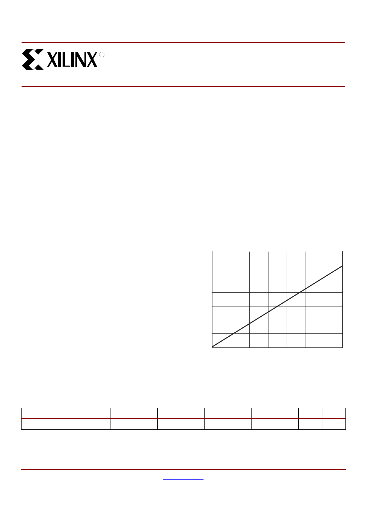
TotalCMOS Design Technique for Fast
Zero Power
Xilinx offers a TotalCMOS CPLD, both in process technology and design technique. Xilinx employs a cascade of
CMOS gates to implement its sum of products instead of
the traditional sense amp approach. This CMOS gate implementation allows Xilinx to offer CPLDs that are both high
performance and low power, breaking the paradigm that to
have low power, you must have low performance. Refer to
Figure 1 and Table 1 showing the I
CC
vs. Frequency of our
XCR3128XL TotalCMOS CPLD (data taken with eight
resetable up/down, 16-bit counters at 3.3V, 25°C).
0
XCR3128XL 128 Macrocell CPLD
DS016 (v1.8) January 8, 2002
014
Preliminary Product Specification
R
Figure 1: Typical ICC vs. Frequency at VCC = 3.3V, 25°C
Frequency (MHz)
DS016_01_112100
Typical I
CC
(mA)
0
0
10
20
30
50
70
40
60
120 140100806040
20
Table 1: Typical ICC vs. Frequency at VCC = 3.3V, 25°C
Frequency (MHz) 0 1 5 10 20 40 60 80 100 120 140
Typical I
CC
(mA) 0 0.5 2.2 4.4 8.7 17.1 25.3 33.6 41.6 49.7 57.7
XCR3128XL 128 Macrocell CPLD
2 www.xilinx.com DS016 (v1.8) Janu ary 8, 2002
1-800-255-7778 Preliminary Product Specification
R
DC Electrical Char acteristics Over Reco mmended Operating Conditions
(1)
Symbol Parameter Test Conditions Min. Max. Unit
V
OH
(2)
Output High voltage IOH = –8 mA 2.4 - V
V
OL
Output Low voltage for 3.3V outputs IOL = 8 mA - 0.4 V
I
IL
Input leakage current VIN = GND or V
CC
–10 10 µA
I
IH
I/O High-Z leakage current VIN = GND or V
CC
–10 10 µA
I
CCSB
Standby current VCC = 3.6V - 100 µA
I
CC
Dynamic current
(3,4)
f = 1 MHz - 1 m A
f = 50 MHz - 30 mA
C
IN
Input pin capacitance
(5)
f = 1 MHz - 8 p F
C
CLK
Clock input capacitance
(5)
f = 1 MHz - 12 pF
C
I/O
I/O pin capacitance
(5)
f = 1 MHz - 10 pF
Notes:
1. See XPLA3 family dat a sheet (
DS012) for recommended operating conditions.
2. See Figure 2 for output drive characteristics of the XPLA3 family.
3. See Table 1, Figure1 for typical values.
4. This parameter measured with a 16-bit, resetable up/down counter loaded into every function block, with all outputs disabled and
unloaded. Inputs are tied to V
CC
or ground. This parameter guaranteed by design and characterization, not testing.
5. Typical values, not tested.
Figure 2: Typical I/V Curve for the XPLA3 Family
0
0
1
0
2
0
30
4
0
50
60
7
0
80
90
1
00
0.51.52.5.54.5
Volt
s
L
3.3V
)
H
3.3V
)
H
2.7V
)
DS012_10_04190
1
XCR3128XL 128 Macrocell CPLD
DS016 (v1.8) January 8, 2002 www.xilinx.com 3
Preliminary Product Specification 1-800-255-7778
R
AC Electrical Characteristics Over Recommended Operating Conditions
(1,2)
Symbol Parameter
-6 -7 -10
Unit Min. Max. Min. Max. Min. Max.
T
PD1
Propagation delay time (single p-term) - 5.5 - 7.0 - 9.1 ns
T
PD2
Propagation delay time (OR array)
(3)
-6.0-7.5-10.0ns
T
CO
Clock to output (global synchronous pin clock) - 4.0 5.0 - 6.5 ns
T
SUF
Setup time (fast input register) 2.5 - 3.0 - 3.0 - ns
T
SU1
(4)
Setup time (single p-term) 3.5 - 4.3 - 5.4 - ns
T
SU2
Setup time (OR array) 4.0 - 4.8 - 6.3 - ns
T
H
(4)
Hold time 0-0-0-ns
T
WLH
(4)
Global Clock pulse width (High or Low) 2.5 - 3.0 - 4.0 - ns
Tt
PLH
(4)
P-term clock pulse width 4.0 - 5.0 - 6.0 - ns
T
R
(4)
Input rise time - 20 - 20 - 20 ns
T
L
(4)
Input fall time - 20 - 20 - 20 ns
f
SYSTEM
(4)
Maximum system frequency - 145 - 119 - 95 MHz
T
CONFIG
(4)
Configuration time
(5)
-60-60-60µs
T
INIT
(4)
ISP initialization tim e - 60 - 60 - 60 µs
T
POE
(4)
P-term OE to output enabled - 7.5 - 9.3 - 11.2 ns
T
POD
(4)
P-term OE to output disabled
(6)
-7.5-9.3-11.2ns
T
PCO
(4)
P-term clock to output - 6.5 - 8.3 - 10.7 ns
T
PAO
(4)
P-term set/reset to output valid - 8.0 - 9.3 - 11.2 ns
Advance Preliminary
Notes:
1. Specificat ions measured with one output switching.
2. See XPLA3 family dat a sheet (
DS012) for recommended operating condi tions.
3. See Figure 4 for derating.
4. These paramet ers guaranteed by design and/or characterization, not test ing.
5. Typical current draw during configuration is 9 mA at 3.6V.
6. Output C
L
= 5 pF.

XCR3128XL 128 Macrocell CPLD
4 www.xilinx.com DS016 (v1.8) Janu ary 8, 2002
1-800-255-7778 Preliminary Product Specification
R
Internal Timing Parameters
(1,2)
Symbol Parameter
-6 -7 -10
UnitMin.
(3)
Max.
(3)
Min. Max. Min. Max.
Buffer Delays
T
IN
Input buffer delay - 1.3 - 1.6 - 2.2 ns
T
FIN
Fast Input buffer delay - 2.3 - 3.0 - 3.1 ns
T
GCK
Global Clock buffer delay - 0.8 - 1.0 - 1.3 ns
T
OUT
Output buffer delay - 2.2 - 2.7 - 3.6 ns
T
EN
Output buffer enable/disable delay - 4.2 - 5.0 - 5.7 ns
Internal Register and Combinatorial Delays
T
LDI
Latch transparent delay - 1.3 - 1.6 - 2.0 ns
T
SUI
Register setup time 1.0 - 1.0 - 1.2 - ns
T
HI
Register hold time 0.3 - 0.5 - 0.7 - ns
T
ECSU
Register clock enable setup time 2.0 - 2.5 - 3.0 - ns
T
ECHO
Register clock enable hold time 3.0 - 4.5 - 5.5 - ns
T
COI
Register clock to putput delay - 1.0 - 1.3 - 1.6 ns
T
AOI
Register async. S/R to output delay - 2.5 - 2.3 - 2.1 ns
T
RAI
Register async. recovery - 4.0 - 5.0 - 6.0 ns
T
LOGI1
Internal logic delay (single p-term) - 2.0 - 2 .7 - 3.3 ns
T
LOGI2
Internal logic delay (PLA OR term) - 2. 5 - 3.2 - 4.2 ns
Feedback Delays
T
F
ZIA delay - 1.7 - 2.1 - 3.0 ns
Time Adders
T
LOGI3
Fold-back NAND delay - 6.0 - 7.5 - 9.5 ns
T
UDA
Universal delay - 1.7 - 2.2 - 2.7 ns
T
SLEW
Slew rate limited delay - 4.0 - 5.0 - 6.0 ns
Advance Preliminary
Notes:
1. These paramete rs guaranteed by design and/or characterization, not testing.
2. See XPLA family dat a sheet (
DS012) for timing model.
3. Con ta c t X ilin x for update on advance specif ication.

XCR3128XL 128 Macrocell CPLD
DS016 (v1.8) January 8, 2002 www.xilinx.com 5
Preliminary Product Specification 1-800-255-7778
R
Switching Characteristics
Figure 3: AC Load Circuit
DS016_03_102401
Component Values
R1 390Ω
R2 390Ω
C1 35 pF
Measurement S1 S2
T
POE
(High)
T
POE
(Low)
T
P
Open Closed
Closed Open
Closed
Closed
V
CC
V
OUT
V
IN
C1
R1
R2
S1
S2
Note: For T
POD
, C1 = 5 pF. Delay measured at
output level of V
OL
+ 300 mV, VOH – 300 mV.
Figure 4: Derating Curve for T
PD2
5.6
5.8
6.0
6.2
6.4
6.6
6.8
7.2
7.0
7.4
1248
DS016_04_042800
16
Number of Adjacent Outputs Switching
ns
Figure 5: Voltage Waveform
90%
10%
1.5 ns 1.5 ns
DS016_05_042800
+3.0V
0V
Measurements:
All circuit delays are measured at the +1.5V level of
inputs and outputs, unless otherwise specified.
T
R
T
L

XCR3128XL 128 Macrocell CPLD
6 www.xilinx.com DS016 (v1.8) Janu ary 8, 2002
1-800-255-7778 Preliminary Product Specification
R
Pin Des cr ip t io ns
Table 2: XCR3128XL User I/O Pins
VQ100 CS144 TQ144
Total User I/O Pins 84 108 108
Table 3: XCR3128XL I/O Pins
Function
Block Macrocell VQ100 CS144 TQ144
1 1 - B12 106
1273
(1)
D11
(1)
104
(1)
1372D12102
1471D13101
1570E10100
1669E1199
1768E1298
18--19--110- -1 11 67 E 13 97
112-F1096
1 13 65 F12 94
1 14 64 F13 93
11563G1092
116-G1191
2175A13107
2276A12109
2377B11110
2478A11111
2579D10112
2680C10113
2781B10114
28--29--210- -21183D9116
21284C9117
21385B9118
214-A9119
215-D8120
216-C8121
31-G1390
3262
(1)
G12
(1)
89
(1)
3361H1388
3460H1287
35-H1186
3658J1384
3757J1283
38--39--310-- 31156J1182
31255J1081
31354K1380
31453K1279
31552K1178
316-K1077
41-M860
4 2 40 L8 61
4341K862
4442N963
4 5 44 L9 65
4645K966
4746N1067
48--49--410-- 41147M1068
4 12 48 L10 69
41349N1170
41450M1171
415-L1172
416-M1274
512A11
521A2143
5 3 100 C3 142
5 4 99 B3 141
5 5 98 A3 140
Table 3: XCR3128XL I/O Pins (Continued)
Function
Block Macrocell VQ100 CS144 TQ 144

XCR3128XL 128 Macrocell CPLD
DS016 (v1.8) January 8, 2002 www.xilinx.com 7
Preliminary Product Specification 1-800-255-7778
R
5 6 97 C4 139
5 7 96 B4 138
58--59--510- -511-A4137
512-D5136
51394B5134
51493A5133
51592D6132
516-C6131
61-B12
624
(1)
D2
(1)
4
(1)
6 3 5D15
6 4 6E46
6 5 7E37
6 6 8E28
6 7 9E19
68--69--610- -6 11 10F410
612-F311
613-F212
6 14 12G214
6 15 13G115
6 16 14G316
71-N756
7 2 37 M7 55
7 3 36 N6 54
7 4 35 M6 53
7 5 33 M5 46
7 6 32 L5 45
7 7 31 K5 44
78--79--710- --
Table 3: XCR3128XL I/O Pins (Continued)
Function
Block Macrocell VQ100 CS144 TQ144
71130N442
7 12 29M441
7 13 28L440
7 14 27K439
715-N338
716-M337
81-H118
8215
(1)
H2
(1)
20
(1)
8316H321
8417H422
85-J123
8619J325
8720J426
88--89--810-- 8 11 21K127
8 12 22K228
8 13 23K329
8 14 24L130
8 15 25M231
816-N132
Notes:
1. JTAG pins
Table 3: XCR3128XL I/O Pins (Continued)
Function
Block Macrocell VQ100 CS144 TQ 144

XCR3128XL 128 Macrocell CPLD
8 www.xilinx.com DS016 (v1.8) Janu ary 8, 2002
1-800-255-7778 Preliminary Product Specification
R
Table 4: XCR3128XL Global, JTA G, P ort Enable, Power ,
and No Connect Pins
Pin Type VQ100 CS144 TQ144
IN0 / CLK0 90 D7 128
IN1 / CLK1 89 C7 127
IN2 / CLK2 88 A7 126
IN3 / CLK3 87 B7 125
TCK 62 G12 89
TDI 4 D2 4
TDO 73 D11 104
TMS 15 H2 20
PORT_EN 11
(1)
F1
(1)
13
(1)
Vcc 3, 18, 34,
39, 51, 66,
82, 91
A10, B2, B6,
B8, D4, F11,
J2, K6, K7,
L13, N5,
N12
24, 50, 51,
58, 73, 76,
95, 115,
123, 130,
144
GND 26, 38, 43,
59, 74, 86,
95
A6, A8, C5,
C13, D3,
G4, H10,
L6, L7, M9,
N2, N8
3, 17, 33,
52, 57, 59,
64, 85, 105,
124, 129,
135
No Connects - B13, C1,
C2, C11,
C12, L2, L3,
L12, M1,
M13, N13
19, 34, 35,
36, 43, 47,
48, 49, 75,
103, 108,
122
Notes:
1. Port Enable is brought Hi gh to enable JTAG pins when JTAG
pins are used as I/O . See family data sheet (
DS012) for full
explanation.
Table 4: XCR3128XL Global, JT A G, P ort Enable, Power ,
and No Co nnect Pins
Pin Type VQ100 CS144 TQ144

XCR3128XL 128 Macrocell CPLD
DS016 (v1.8) January 8, 2002 www.xilinx.com 9
Preliminary Product Specification 1-800-255-7778
R
Ordering Information
Component Availability
XCR3128XL -7 VQ 100 C
Example:
Temperature Range
Number of Pins
Package Type
Device Type
Speed Grade
Device Ordering Options
Speed Package Temperature
-10 10 ns pin-to-pin delay VQ100 100-pin Very Thin Quad Flat Package C = Commercial T
A
= 0°C to +70°C
V
CC
= 3.0V to 3.6V
-7 7.5 ns pin-to-pin delay CS144 144-ball Chip Scale Package I = Industrial T
A
= –40°C to +85°C
V
CC
= 2.7V to 3.6V
-6 6 ns pin-to-pin del ay TQ144 144-pin Thin Quad Fl at Pack
Pins 100 144 144
Type Plastic VQFP Pla stic TQFP Plastic BGA
Code VQ100 TQ144 CS144
XCR3128XL
-6 (C) (C) (C)
-7 C, (I) C, (I) C, (I)
-10 C,I C,I C,I
Notes:
1. Parenthesis indicate future planned products. Please contact Xilinx for up-to-date information.

XCR3128XL 128 Macrocell CPLD
10 www.xilinx.com DS016 (v1.8) Janu ary 8, 2002
1-800-255-7778 Preliminary Product Specification
R
Revision History
The following table shows the revision history for this document.
Date Version Revision
04/07 /00 1.0 Init ial Xilinx relea s e.
05/03/00 1.1 M inor updates and added B oundary Scan to pinout table.
11/20/00 1.2 Upda ted pinout tables; corrected note in Table 4 to read: "port enable pin is brought High".
12/08/00 1.3 Updated pinout tables.
01/17/01 1.4 Removed Timing Model.
04/11/01 1.5 Added Typical I/V curve, Figure 2; added Table 2: Total User I/O; changed V
OH
spec.
04/19/01 1.6 Updated Typi c al I/V cur ve, Figure 2: added voltage levels.
08/10/01 1.7 M oved Figure 1 and Table 1 to first page. Changed VQ144 to VQ100 in Table 2.
01/08/02 1.8 Updated T
SUF
and T
FIN
spec to match software timing. Added single p-term setup time
(T
SU1
) to AC Table, renamed TSU to T
SU2
for setup time through the OR arr ay. Added T
INIT
spec . Up dat ed T
CONFIG
spec. Updated THI spec to correct a typo. Updated AC Load Circuit
diagram to more closely resemble true test conditions, added note for T
POD
delay
measurement.
 Loading...