XILINX XC95216-20PQ160I, XC95216-20PQ160C, XC95216-20HQ208I, XC95216-20HQ208C, XC95216-10HQ208I Datasheet
...
August 21, 2001 (Version 3.1) 1
Features
• 10 ns pin-to- pin log ic delays on all pins
•f
CNT
to 111 MHz
• 216 ma c r oc el ls wit h 48 00 usable gates
• Up to 16 6 us er I /O pin s
• 5 V in-system programmable
- Endurance of 10,000 program/erase cycl es
- Program/erase over full commer cial voltage and
temperature range
• Enhanced pin-locking a rchitecture
• Flexible 36V18 Function Block
- 90 product terms drive any or all of 18 macrocells
within Function Block
- Global and product term clocks, output enables, set
and reset signals
• Extensive IEEE Std 1149.1 bounda ry- scan (JTAG)
support
• Programmable power reduction mode in each
macrocell
• Slew rate control on individual outputs
• User programmable ground pin capability
• Extended pattern security features for design protection
• High -drive 24 mA outputs
• 3.3 V or 5 V I/O capability
• Ad vanc e d CMO S 5V Fast FL A SH tec hn ology
• Supports parallel programming of more than one
XC9500 concurrently
• Available in 160-pin PQFP, 352-pin BGA, and 208-pin
HQFP pa ckages
Description
The XC95216 is a high-performance CPLD providing
advanced in-system programming and test capabilities for
gener al pu rpose lo gic integr a tion. It is c om p r i se d o f twelve
36V1 8 Func tion Blo cks, prov id ing 4 ,800 usable gat es wit h
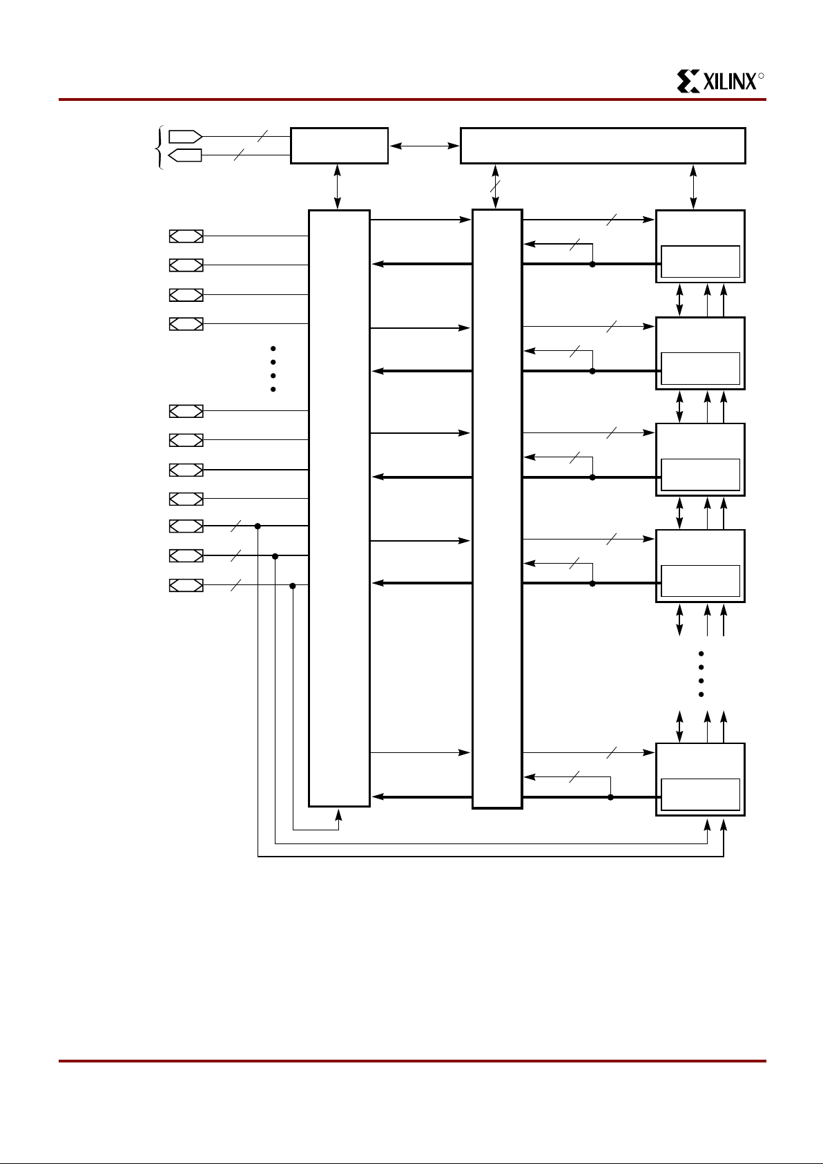
propagation delays of 10 ns. See Figure 2 for the architec-
ture overview.
Power Managemen t
Power diss ipation c an be reduced in t h e XC95216 by configuring macrocells to standard or low-power modes of
operation. Unused macrocells are turned off to minimize
power dissipation.
Opera t in g cu r re nt for eac h design can be ap pr ox im ate d for
spec ifi c op er at in g co nditions us in g the following eq ua tio n:
I
CC
(mA) =
MC
HP
(1.7) + MCLP (0.9) + MC (0.006 mA/MHz) f
Where:
MC
HP
= Macrocells in high-performance mode
MC
LP
= Macrocells in low-power mode
MC = Total number of macrocells used
f = Clock frequency (MHz)
Figure 1 shows a typical calculation for the XC95216
device.
1
XC95216 In-System Programmable
CPLD
Augu st 21 , 20 0 1 (V e r si on 3.1)
10*
Product Specification
Clock Frequency (MHz)
Typical I
CC
(mA)
050
200
(360)
(500)
(340)
400
600
100
H
igh P
erform
ance
Low Power
X5918
Figure 1: Typical ICC vs. Frequency For XC95216

R
XC95216 In-System Programmable CPLD
2 August 2 1, 2001 (Version 3.1)
In-System Programming Controller
JTAG
Controller
I/O
Blocks
Function
Block 1
Macrocells
1 to 18
Macrocells
1 to 18
Macrocells
1 to 18
Macrocells
1 to 18
JTAG Port
3
36
I/O/GTS
I/O/GSR
I/O/GCK
I/O
I/O
I/O
I/O
2
1
I/O
I/O
I/O
I/O
3
X5917
1
Function
Block 2
36
Function
Block 3
36
Function
Block 4
36
Macrocells
1 to 18
Function
Block 12
36
18
18
18
18
18
FastCONNECT Switch Matrix
Figure 2: XC95216 Architecture
Function Block outputs (indicated by the bold line) drive the I/O Blocks directly

R
August 21, 2001 (Version 3.1) 3
XC95216 In-System Programmable CPLD
Absolute Maximum Rati ngs
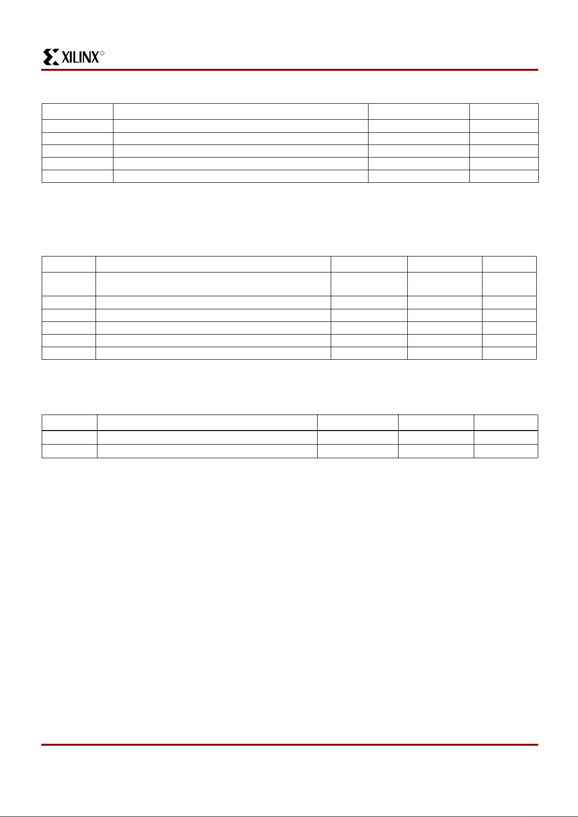
Warning: Stresses beyond those listed under Absolute Maximum Ratings may cause permanent damage to the device. These are
stress ratings only, and functional operation of the device at these or any other conditions beyond those listed under
Recommended Operating Conditions is not implied. Exposure to Absolute Maximum Rating conditions for extended periods
of time may affect device reliability.
Recommended Operating Conditions
1
Note: 1. Numbers in parenthesis are for industrial-temperature range versions.
Endurance Characteristics
Symbol Parameter Value Units
V
CC
Supply voltage relat ive to GND -0.5 to 7.0 V
V
IN
DC input vo ltage relative to GND -0.5 to VCC + 0.5 V
V
TS
Voltage applied to 3-state output with respect to GND -0.5 to VCC + 0.5 V
T
STG
Storage temperature -65 to +150 °C
T
SOL
Max soldering temperature (10 s @ 1/1 6 in = 1.5 m m) +260 °C
Symbol Parameter Min Max Units
V
CCINT
Supply voltage for internal logic and input buffer 4.75
(4.5)
5.25
(5.5)
V
V
CCIO
Supply voltage for output drivers for 5 V operation 4.75 (4.5) 5.25 (5.5) V
Supply voltage for output drivers for 3.3 V operation 3.0 3.6 V
V
IL
Low-level input voltage 0 0.80 V
V
IH
High-level input voltage 2.0 V
CCINT
+0.5 V
V
O
Output voltage 0 V
CCIO
V
Symbol Parameter Min Max Units
t
DR
Data Retention 20 - Years
N
PE
Program/Erase Cycles 10,00 0 - Cycles
 Loading...