

Datasheet XC95108-7PQ160I, XC95108-7PQ160C, XC95108-7PQ100I, XC95108-7PQ100C, XC95108-7PC84I Datasheet (XILINX)
...
December 4, 1998 (Version 3.0) 1
Features
• 7.5 ns pin-to-pin logic delays on all pins
•f
CNT
to 125 MHz
• 108 macrocells with 2400 usable gates
• Up to 108 user I/O pins
• 5 V in-system programmable (ISP)
- Endurance of 10,000 program/erase cycles
- Program/erase over full commercial voltage and
temperature range
• Enhanced pin-locking architecture
• Flexible 36V18 Function Block
- 90 product terms drive any or all of 18 macrocells
within Function Block
- Global and product term clocks, output enables, set
and reset signals
• Extensive IEEE Std 1149.1 boundary-scan (JTAG)
support
• Programmable power reduction mode in each
macrocell
• Slew rate control on individual outputs
• User programmable ground pin capability
• Extended pattern security features for design protection
• High-drive 24 mA outputs
• 3.3 V or 5 V I/O capability
• Advanced CMOS 5V FastFLASH technology
• Supports parallel programming of more than one
XC9500 concurrently
• Available in 84-pin PLCC, 100-pin PQFP, 100-pin TQFP
and 160-pin PQFP packages
Description
The XC95108 is a high-performance CPLD providing
advanced in-system programming and test capabilities for
general purpose logic integration. It is comprised of six
36V18 Function Blocks, providing 2,400 usable gates with
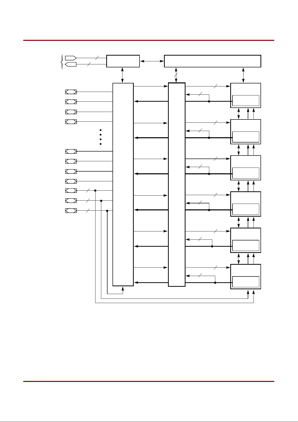
propagation delays of 7.5 ns. See Figure2 for the architecture overview.
Power Management
Power dissipation can be reduced in the XC95108 by configuring macrocells to standard or low-power modes of
operation. Unused macrocells are turned off to minimize
power dissipation.
Operating current for each design can be approximated for
specific operating conditions using the following equation:
I
CC
(mA) =
MC
HP
(1.7) + MCLP (0.9) + MC (0.006 mA/MHz) f
Where:
MC
HP
= Macrocells in high-performance mode
MC
LP
= Macrocells in low-power mode
MC = Total number of macrocells used
f = Clock frequency (MHz)
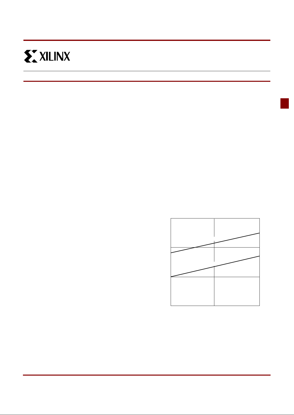
Figure1 shows a typical calculation for the XC95108
device.
1
XC95108 In-System Programmable
CPLD
December 4, 1998 (Version 3.0)
11*
Product Specification
Clock Frequency (MHz)
Typical I
CC
(mA)
050
100
(180)
(250)
(170)
200
300
100
High Performance
Low Power
X5898
Figure 1: Typical ICC vs. Frequency for XC95108
XC95108 In-System Programmable CPLD
2 December 4, 1998 (Version 3.0)
In-System Programming Controller
JTAG
Controller
I/O
Blocks
Function
Block 1
Macrocells
1 to 18
Macrocells
1 to 18
Macrocells
1 to 18
Macrocells
1 to 18
JTAG Port
3
36
I/O/GTS
I/O/GSR
I/O/GCK
I/O
I/O
I/O
I/O
2
1
I/O
I/O
I/O
I/O
3
X5897
1
Function
Block 2
36
Function
Block 3
36
Function
Block 4
36
Macrocells
1 to 18
Function
Block 5
36
Macrocells
1 to 18
Function
Block 6
36
18
18
18
18
18
18
FastCONNECT Switch Matrix
Figure 2: XC95108 Architecture
Note:
Function Block outputs (indicated by the bold line) drive the I/O Blocks directly
December 4, 1998 (Version 3.0) 3
XC95108 In-System Programmable CPLD
Absolute Maximum Ratings
Warning:Stresses beyond those listed under Absolute Maximum Ratings may cause permanent damage to the device. These are
stress ratings only, and functional operation of the device at these or any other conditions beyond those listed under
Recommended Operating Conditions is not implied. Exposure to Absolute Maximum Rating conditions for extended periods
of time may affect device reliability.
Recommended Operation Conditions
1
Note: 1. Numbers in parenthesis are for industrial-temperature range versions.
Endurance Characteristics
Symbol Parameter Value Units
V
CC
Supply voltage relative to GND -0.5 to 7.0 V
V
IN
DC input voltage relative to GND -0.5 to VCC + 0.5 V
V
TS
Voltage applied to 3-state output with respect to GND -0.5 to VCC + 0.5 V
T
STG
Storage temperature -65 to +150 °C
T
SOL
Max soldering temperature (10 s @ 1/16 in = 1.5 mm) +260 °C
Symbol Parameter Min Max Units
V
CCINT
Supply voltage for internal logic and input buffer 4.75
(4.5)
5.25
(5.5)
V
V
CCIO
Supply voltage for output drivers for 5 V operation 4.75 (4.5) 5.25 (5.5) V
Supply voltage for output drivers for 3.3 V operation 3.0 3.6 V
V
IL
Low-level input voltage 0 0.80 V
V
IH
High-level input voltage 2.0 V
CCINT
+0.5 V
V
O
Output voltage 0 V
CCIO
V
Symbol Parameter Min Max Units
t
DR
Data Retention 20 - Years
N
PE
Program/Erase Cycles 10,000 - Cycles

XC95108 In-System Programmable CPLD
4 December 4, 1998 (Version 3.0)
DC Characteristics Over Recommended Operating Conditions
AC Characteristics
Note: 1. f
CNT
is the fastest 16-bit counter frequency available, using the local feedback when applicable.
f
CNT
is also the Export Control Maximum flip-flop toggle rate, f
TOG
.
2. f
SYSTEM
is the internal operating frequency for general purpose system designs spanning multiple FBs.
Symbol Parameter Test Conditions Min Max Units
V
OH
Output high voltage for 5 V operation IOH = -4.0 mA
V
CC
= Min
2.4 V
Output high voltage for 3.3 V operation I
OH
= -3.2 mA
V
CC
= Min 2.4
V
V
OL
Output low voltage for 5 V operation IOL = 24 mA
V
CC
= Min
0.5 V
Output low voltage for 3.3 V operation I
OL
= 10 mA
V
CC
= Min
0.4 V
I
IL
Input leakage current VCC = Max
V
IN
= GND or V
CC
±10.0 µA
I
IH
I/O high-Z leakage current VCC = Max
V
IN
= GND or V
CC
±10.0 µA
C
IN
I/O capacitance VIN = GND
f = 1.0 MHz
10.0 pF
I
CC
Operating Supply Current
(low power mode, active)
VI = GND, No load
f = 1.0 MHz
100 (Typ) ma
Symbol Parameter
XC95108-7 XC95108-10XC95108-15 XC95108-20
Units
Min Max Min Max Min Max Min Max
t
PD
I/O to output valid 7.5 10.0 15.0 20.0 ns
t
SU
I/O setup time before GCK 4.5 6.0 8.0 10.0 ns
t
H
I/O hold time after GCK 0.0 0.0 0.0 0.0 ns
t
CO
GCK to output valid 4.5 6.0 8.0 10.0 ns
f
CNT
1
16-bit counter frequency 125.0 111.1 95.2 83.3 MHz
f
SYSTEM
2
Multiple FB internal operating frequency 83.3 66.7 55.6 50.0 MHz
t
PSU
I/O setup time before p-term clock input 0.5 2.0 4.0 4.0 ns
t
PH
I/O hold time after p-term clock input 4.0 4.0 4.0 6.0 ns
t
PCO
P-term clock to output valid 8.5 10.0 12.0 16.0 ns
t
OE
GTS to output valid 5.5 6.0 11.0 16.0 ns
t
OD
GTS to output disable 5.5 6.0 11.0 16.0 ns
t
POE
Product term OE to output enabled 9.5 10.0 14.0 18.0 ns
t
POD
Product term OE to output disabled 9.5 10.0 14.0 18.0 ns
t
WLH
GCK pulse width (High or Low) 4.0 4.5 5.5 5.5 ns

December 4, 1998 (Version 3.0) 5
XC95108 In-System Programmable CPLD
Internal Timing Parameters
Note: 3. t
PTA
is multiplied by the span of the function as defined in the family data sheet.
Symbol Parameter
XC95108-7 XC95108-10XC95108-15 XC95108-20
Units
Min Max Min Max Min Max Min Max
Buffer Delays
t
IN
Input buffer delay 2.5 3.5 4.5 6.5 ns
t
GCK
GCK buffer delay 1.5 2.5 3.0 3.0 ns
t
GSR
GSR buffer delay 4.5 6.0 7.5 9.5 ns
t
GTS
GTS buffer delay 5.5 6.0 11.0 16.0 ns
t
OUT
Output buffer delay 2.5 3.0 4.5 6.5 ns
t
EN
Output buffer enable/disable delay 0.0 0.0 0.0 0.0 ns
Product Term Control Delays
t
PTCK
Product term clock delay 3.0 3.0 2.5 2.5 ns
t
PTSR
Product term set/reset delay 2.0 2.5 3.0 3.0 ns
t
PTTS
Product term 3-state delay 4.5 3.5 5.0 5.0 ns
Internal Register and Combinatorial delays
t
PDI
Combinatorial logic propagation delay 0.5 1.0 3.0 4.0 ns
t
SUI
Register setup time 1.5 2.5 3.5 3.5 ns
t
HI
Register hold time 3.0 3.5 4.5 6.5 ns
t
COI
Register clock to output valid time 0.5 0.5 0.5 0.5 ns
t
AOI
Register async. S/R to output delay 6.5 7.0 8.0 8.0 ns
t
RAI
Register async. S/R recovery before clock 7.5 10.0 10.0 10.0 ns
t
LOGI
Internal logic delay 2.0 2.5 3.0 3.0 ns
t
LOGILP
Internal low power logic delay 10.0 11.0 11.5 11.5 ns
Feedback Delays
t
F
FastCONNECT matrix feedback delay 8.0 9.5 11.0 13.0 ns
t
LF
Function Block local feeback delay 4.0 3.5 3.5 5.0 ns
Time Adders
t
PTA
3
Incremental Product Term Allocator delay 1.0 1.0 1.0 1.5 ns
t
SLEW
Slew-rate limited delay 4.0 4.5 5.0 5.5 ns
R
1
V
TEST
C
L
R
2
Device Output
Output Type V
TEST
5.0 V
3.3 V
R
1
160 Ω
260 Ω
R
2
120 Ω
360 Ω
C
L
35 pF
35 pF
X5906
V
CCIO
5.0 V
3.3 V
Figure 3: AC Load Circuit

XC95108 In-System Programmable CPLD
6 December 4, 1998 (Version 3.0)
XC95108 I/O Pins
Notes: [1] Global control pin
Function
Block
Macrocell PC84 PQ100 TQ100PQ160
BScan
Order
Notes
Function
Block
Macrocell PC84 PQ100 TQ100PQ160
BScan
Order
Notes
1 1 – – – 25 321 3 1 – – – 45 213
1 2 1 15 13 21 318 3 2 14 31 29 47 210
1 3 2 16 14 22 315 3 3 15 32 30 49 207
1 4 – 21 19 29 312 3 4 – 36 34 57 204
1 5 3 17 15 23 309 3 5 17 34 32 54 201
1 6 4 18 16 24 306 3 6 18 35 33 56 198
1 7 – – – 27 303 3 7 – – – 50 195
1 8 5 19 17 26 300 3 8 19 37 35 58 192
1 9 6 20 18 28 297 3 9 20 38 36 59 189
1 10 – 26 24 36 294 3 10 – 45 43 69 186
1 11 7 22 20 30 291 3 11 21 39 37 60 183
1 12 9 24 22 33 288 [1] 3 12 23 41 39 62 180
1 13 – – – 34 285 3 13 – – – 52 177
1 14 10 25 23 35 282 [1] 3 14 24 42 40 63 174
1 15 11 27 25 37 279 3 15 25 43 41 64 171
1 16 12 29 27 42 276 [1] 3 16 26 44 42 68 168
1 17 13 30 28 44 273 3 17 31 51 49 77 165
1 18 – – – 43 270
3 18 – – – 74 162
2 1 – – – 158 267 4 1 – – – 123 159
2 2 71 98 96 154 264 4 2 57 83 81 134 156
2 3 72 99 97 156 261 4 3 58 84 82 135 153
2 4 – 4 2 4 258 4 4 – 82 80 133 150
2 5 74 1 99 159 255 [1] 4 5 61 87 85 138 147
2 6 75 3 1 2 252 4 6 62 88 86 139 144
2 7 – – – 9 249 4 7 – – – 128 141
2 8 76 5 3 6 246 [1] 4 8 63 89 87 140 138
2 9 77 6 4 8 243 [1] 4 9 65 91 89 142 135
2 10 – 9 7 12 240 4 10 – – – 147 132
2 11 79 8 6 11 237 4 11 66 92 90 143 129
2 12 80 10 8 13 234 4 12 67 93 91 144 126
2 13 – – – 14 231 4 13 – – – 153 123
2 14 81 11 9 15 228 4 14 68 95 93 146 120
2 15 82 12 10 17 225 4 15 69 96 94 148 117
2 16 83 13 11 18 222 4 16 – 94 92 145 114
2 17 84 14 12 19 219 4 17 70 97 95 152 111
2 18 – – – 16 216
4 18 – – – 155 108

December 4, 1998 (Version 3.0) 7
XC95108 In-System Programmable CPLD
XC95108 I/O Pins (continued)
XC95108 Global, JTAG and Power Pins
Function
Block
Macrocell PC84 PQ100 TQ100PQ160
BScan
Order
Notes
Function
Block
Macrocell PC84 PQ100 TQ100PQ160
BScan
Order
Notes
5 1 – – – 76 105 6 1 – – –9151
5 2 32 52 50 79 102 6 2 45 67 65 103 48
5 3 33 54 52 82 99 6 3 46 68 66 104 45
5 4 – 48 46 72 96 6 4 – 75 73 116 42
5 5 34 55 53 86 93 6 5 47 69 67 106 39
5 6 35 56 54 88 90 6 6 48 70 68 108 36
5 7 – – –7887 6 7 – – – 105 33
5 8 36 57 55 90 84 6 8 50 72 70 111 30
5 9 37 58 56 92 81 6 9 51 73 71 113 27
5 10 – – –8478 6 10 – – – 107 24
5 11 39 60 58 95 75 6 11 52 74 72 115 21
5 12 40 62 60 97 72 6 12 53 76 74 117 18
5 13 – – –8769 6 13 – – – 112 15
5 14 41 63 61 98 66 6 14 54 78 76 122 12
5 15 43 65 63 101 63 6 15 55 79 77 124 9
5 16 – 61 59 96 60 6 16 – 81 79 129 6
5 17 44 66 64 102 57 6 17 56 80 78 126 3
5 18 – – – 89 54
6 18 – – – 114 0
Pin Type PC84 PQ100 TQ100 PQ160
I/O/GCK1 9 24 22 33
I/O/GCK2 10 25 23 35
I/O/GCK3 12 29 27 42
I/O/GTS1 76 5 3 6
I/O/GTS2 77 6 4 8
I/O/GSR 74 1 99 159
TCK30504875
TDI28474571
TDO 59 85 83 136
TMS29494773
V
CCINT
5 V 38,73,78 7,59,100 5,57,98 10,46,94,157
V
CCIO
3.3 V/5 V 22,64 28,40,53,90 26,38,51,88 1,41,61,81,121,141
GND 8,16,27,42,49,60 2,23,33,46,64,71,77,86 100,21,31,44,62,69,75,84 20,31,40,51,70,80,99
GND – – – 100,110,120,127,137
GND – – – 160
No connects – – – 3,5,7,32,38,39,48,53,55,6
5,66,67,83,85,93,109,
118,119,125,130,131,
132,149,150,151

XC95108 In-System Programmable CPLD
8 December 4, 1998 (Version 3.0)
Ordering Information
Component Availability
C = Commercial = 0° to +70°C I = Industrial = –40° to +85°C
Revision Control
Speed Options
- 2020 ns pin-to-pin delay
-1515 ns pin-to-pin delay
-1010 ns pin-to-pin delay
-7 7 ns pin-to-pin delay
Packaging Options
PC84 84-Pin Plastic Leaded Chip Carrier (PLCC)
PQ100100-Pin Plastic Quad Flat Pack (PQFP)
TQ100100-Pin Very Thin Quad Flat Pack (TQFP)
PQ160160-Pin Plastic Quad Flat Pack (PQFP)
Temperature Options
C Commercial 0°C to +70°C
I Industrial –40°C to +85°C
XC95108 -7 PQ 160 C
Device Type
Speed
Package Type
Number of Pins
Temperature Range
Pins 84 100 160
Type
Plastic
PLCC
Plastic
PQFP
Plastic
TQFP
Plastic
PQFP
Code PC84 PQ100 TQ100 PQ160
XC95108
–20 C(I) C(I) C(I) C(I)
–15 C(I) C(I) C(I) C(I)
–10 C(I) C(I) C(I) C(I)
–7 C(I) C(I) C(I) C(I)
Date Revision
12/04/98 Update AC Characteristics and Internal Parameters
 Loading...