XILINX XC5215-5PG299C, XC5215-5HQ240C, XC5215-5HQ208C, XC5215-5BG352C, XC5215-5BG225C Datasheet
...
November 5, 1998 (Version 5.2) 7-83
7
Features
• Low-cost, register/latch rich, SRAM based
reprogrammable architecture
-0.5µm three-layer metal CMOS process technology
- 256 to 1936 logic cells (3,000 to 23,000 “gates”)
- Price competitive with Gate Arrays
• System Le vel Features
- System performance beyond 50 MHz
- 6 levels of interconnect hierarchy
- VersaRing
™
I/O Interface for pin-locking
- Dedicated carry logic for high-speed arithmetic
functions
- Cascade chain for wide input fun ctions
- Built-in IEEE 1149.1 JTAG boundary scan test
circuitry on all I/O pins
- Internal 3-state bussin g ca pa bilit y
- Four dedicated low-skew clock or signal distribution
nets
• Versatile I/O and Packaging
- Innovative VersaRi ng
™
I/O interface provides a high
logic cell to I/O ratio, with up to 244 I/O signals
- Programmable output slew-rate control maximizes
performance and reduces noise
- Zero Flip-Flop hold time for input registers simplifies
system timing
- Independent Output Enables for external bussing
- Footprint compatibility in co mm o n packages within
the XC5200 Series and with the XC4000 Series
- Over 150 device/package combinations, including
advanced BGA, TQ, and VQ packaging available
• Fully Supported by Xilinx Development System
- Automatic place and route software
- Wide selection of PC and Workstation platfor m s
- Over 100 3rd-party Allian ce interf ace s
- Supported by shrink-wrap Foundation software
Description
The XC5200 Field-Programmable Gate Array Family is
engineered to deliver low cost. Building on experiences
gained with three previous successful SRAM FPGA families, the XC5200 family brings a robust feature set to programmable logic design. The VersaBlock
™
logic module,
the VersaRing I/O interface, and a rich hierarchy of interconnect resources combine to enhance design flexibility
and reduce time-to-market. Complete support for the
XC5200 family is delivered th rough t he familiar Xilinx soft ware environme nt. The XC52 00 fa mily is f ully suppo rted on
popular workstation and PC platforms. Popular design
entry methods are fully supported, includ ing ABEL, schematic capture, VHDL, and Verilog HDL synthesis. Designers utilizing logic s ynthesis can use their existing tools to
design with th e XC5200 device s.
.
0
XC5200 Series
Field Programmable Gate Arrays
November 5, 1998 (Version 5.2)
07*
Product Specification
R
Table 1: XC5200 Field-Programmable Gate Array Family Members
Device XC5202 XC5204 XC5206 XC5210 XC5215
Logic Cells 256 480 784 1,296 1,936
Max Logic Gates 3,000 6,000 10,000 16,000 23,000
Typical Gate Range 2,000 - 3,000 4,000 - 6,000 6,000 - 10,000 10,000 - 16,000 15,000 - 23,000
VersaBlock Array 8 x 8 10 x 12 14 x 14 18 x 18 22 x 22
CLBs 64 120 196 324 484
Flip-Flops 256 480 784 1,296 1,936
I/Os 84 124 148 196 244
TBUFs per Longline 1014162024

R
XC5200 Series Field Programmable Gate Arrays
7-84 November 5, 1998 (Version 5.2)
XC5200 Family Compared to
XC4000/Spartan™ and XC3000
Series
For readers already f amiliar with the XC4000/Spa rtan and
XC3000 FPGA Families, this section describes sig nificant
differences between them and the XC5200 family. Unless
otherwise indicated, comparisons refer to both
XC4000/Spartan and XC3000 devices.
Configurable Logic Block (CLB) Resources
Each XC5200 CLB cont ai n s fo ur i nde pe nde nt 4- i np ut fu nction generators and four registers, which are configured as
four indepe ndent Log ic Ce lls™ ( LCs). T he regi sters in eac h
XC5200 LC are optionally configurable as edge-triggered
D-type flip-flops or as transparent level-sensitive latches.
The XC5200 CLB includes dedicated carry logic that provides fast arithmetic ca rry capability. The dedicated carry
logic may also be used to cascade function generators for
implementing wide arithmetic functions.
XC4000 family:
XC5200 devices have no wide edge
decoders. Wide decoders are implemented using cascade
logic. Although sa crificing spe ed for s ome desig ns, lack of
wide edge decoders reduces the die area and hence cost
of the XC5200.
XC4000/Spartan family:
XC5200 dedicated carry logic
differs from that o f the XC4000/Spar tan family in that the
sum is generated in an additional function generator in the
adjacent column. This design reduces XC5200 die size and
hence cost for many applications. Note, however, that a
loadable up/down counter requires the same number of
function gener ators in bo th families . XC3000 has no d edicated carry.
XC4000/Spartan family:
XC5200 lookup tables are opti-
mized for cost and hence cannot implement RAM.
Input/Output Block (IOB) Resources
The XC5200 family maintains footprint compatibility with
the XC4000 family, but not with the XC3000 family.
T o minimize cost and maximize the number of I/O per Logic
Cell, the XC5200 I/O does not include flip-flops or latches.
For high performance paths, the XC5200 family provides
direct connections from each IOB to the registers in the
adjacent CLB in order to emulate IOB registers.
Each XC5200 I/O Pin provides a programmable delay element to control input set -up tim e. This element ca n be used
to avoid potential hold-time problems. Each XC5200 I/O
Pin is capable of 8-mA source and sink currents.
IEEE 1149.1-type boundary scan is supported in each
XC5200 I/O.
Routing Resources
The XC5200 family provides a flexible coupling of logic and
local routing res ourc es cal led the VersaBl ock. The XC520 0
Versa Block elemen t incl udes the CLB, a Local Inte rconne ct
Matrix (LIM), and direct connects to neighboring VersaBlocks.
The XC5200 provides four global buffers for clocking or
high-fanout co nt ro l si gna l s. E ach bu ffer may be sou rc ed by
means of its dedicated pad or from any internal source.
Each XC5200 TBUF ca n dr ive up t o two h oriz o nt al a nd t wo
vertical Longlines. There are no internal pull-ups for
XC5200 Longlines.
Configuration and Readback
The XC5200 supports a new configuration mode called
Express mode.
XC4000/Spartan family:
The XC5200 family provides a
global reset but not a global set.
XC5200 devices use a different configuration process than
that of the XC 3000 f ami ly, but use th e s ame p ro ce ss as th e
XC4000 and Spartan families.
XC3000 family:
Although their configuration processes differ, XC5200 devices may be used in daisy chains with
XC3000 devices.
XC3000 family:
The XC5200 PROGRAM pin is a single-function input pin that overrides all other inputs. The
PROGRAM pin does not exist in XC3000.
Table 2: Xilinx Field-Programmable Gate Array
Families
Parameter XC5200 Spartan XC4000 XC3000
CLB function
generators
4332
CLB inputs 20 9 9 5
CLB outputs 12 4 4 2
Global buffers 4 8 8 2
User RAM no yes yes no
Edge decoders no no yes no
Cascade chain yes no no no
Fast carry logic yes yes yes no
Internal 3-state yes yes yes yes
Boundary scan yes yes yes no
Slew-rate control yes yes yes yes
R
November 5, 1998 (Version 5.2) 7-85
XC5200 Series Field Programmable Gate Arrays
7
XC3000 family:
XC5200 devices support an additional pro -
gramming mode: Peripheral Synchronous.
XC3000 family:
The XC5200 family does not support
Power-down, but of f ers a Glo bal 3- state input that does not
reset any flip-flops.
XC3000 family:
The XC5200 family does not provide an
on-chip crystal oscillato r amplifier, but it does provide an
internal oscillator from which a variet y of fre quencie s up to
12 MHz are available.
Architectural Overview
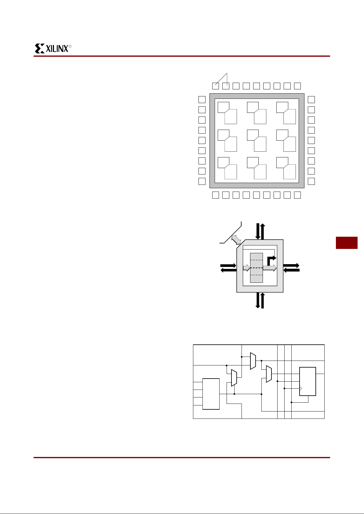
Figure 1 presents a simplified, conceptual overview of the
XC5200 architecture. Similar to conventional FPGAs, the
XC5200 family consists of programmable IOBs, programmable logic blocks, and programmable interconnect. Unlike
other FPGAs, however, the logic and local routing
resources of th e XC5200 family are combined in flexible
VersaBlocks (Figure 2). General-purpose routing connects
to the VersaBlock through the General Routing Matrix
(GRM).
VersaBlock: Abundant Local Routing Plus
V ersatile Log ic
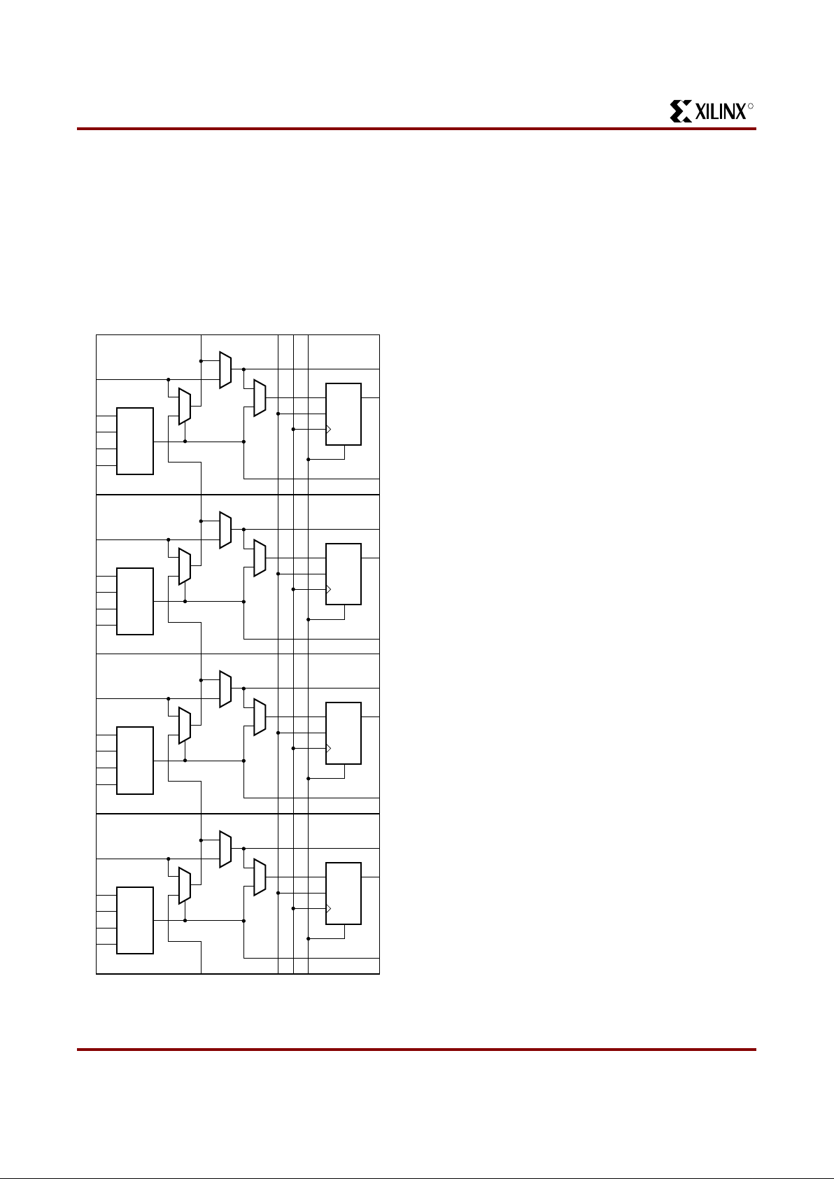
The basic logic el emen t in ea ch VersaBlock structure is t he
Logic Cell, shown in Figure 3. Each LC contains a 4-input
function generator (F), a storage device (FD), and control
logic. There are five independent inputs and three outputs
to each LC. The independence of the inputs and outputs
allows the software to maximize the resource utilization
within each LC. Each Logic Cell also contains a direct
feedthrough path that does not sacrifice the use of either
the function gen erator or th e register ; this featu re is a first
for FPGAs. The st orage devic e is configu rable as eit her a D
flip-flop or a latch. The control logic consists of carry logic
for fast implementation of arithmetic functions, which can
also be configured as a cascade chain allowing decode of
very wide input functions.
Figure 1: XC5200 Architectural Overview
Figure 2: VersaBlock
Figure 3: XC5200 Logic Cell (Four LCs per CLB)
X4955
GRM
Input/Output Blocks (IOBs)
Versa-
Block
GRM
Versa-
Block
VersaRing
VersaRing
GRM
Versa-
Block
GRM
Versa-
Block
GRM
Versa-
Block
GRM
Versa-
Block
GRM
Versa-
Block
GRM
Versa-
Block
GRM
Versa-
Block
VersaRing
VersaRing
X5707
CLB
Direct Connects
TS
GRM
LIM
4
4
4
4
4
LC3
LC2
LC1
LC0
44
44
24
24
X4956
F4
F3
F
FD
F2
F1
DQ
X
DO
DI
CO
CI CE CK CLR
R
XC5200 Series Field Programmable Gate Arrays
7-86 November 5, 1998 (Version 5.2)
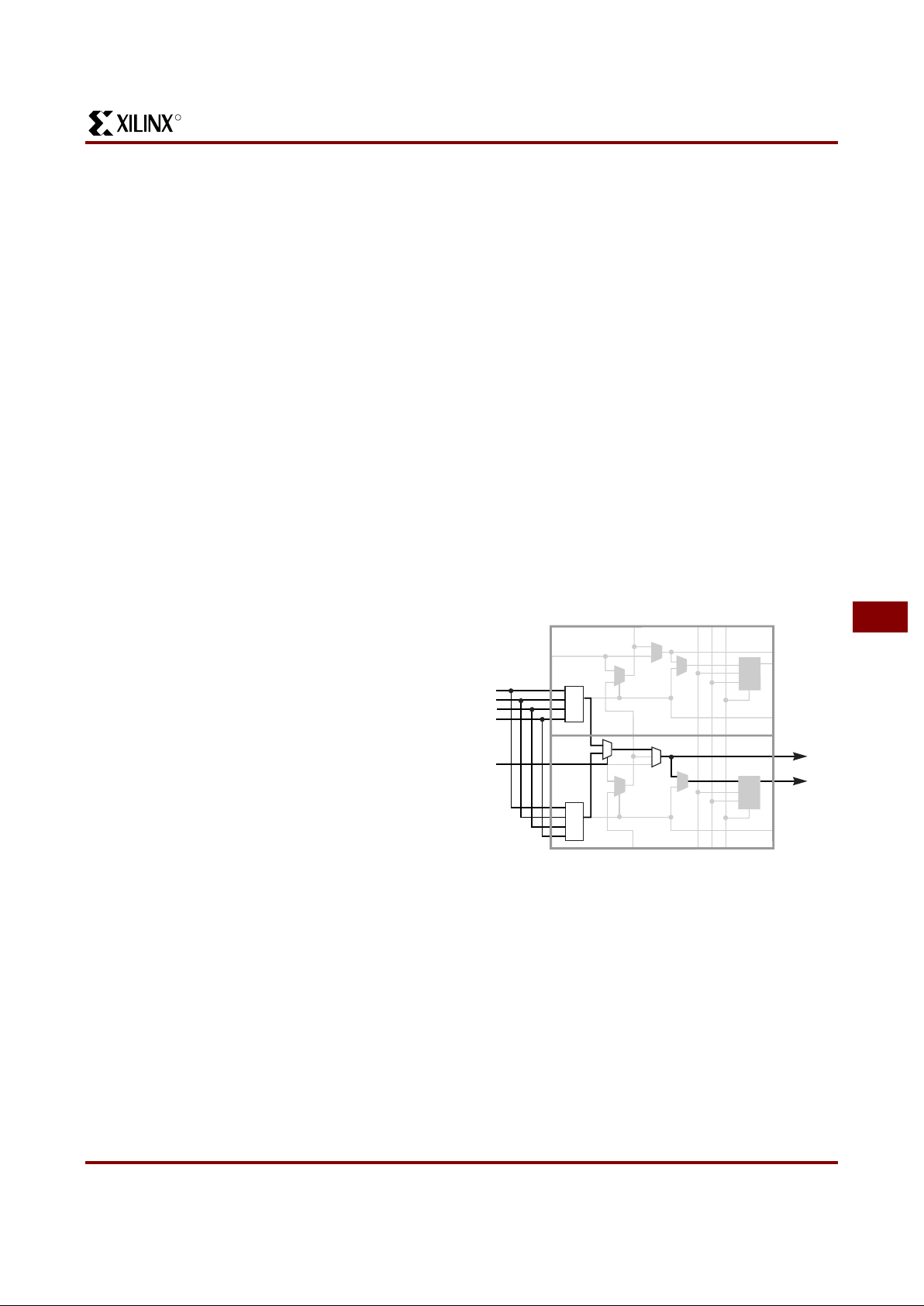
The XC5200 CLB consists of four LCs, as shown in
Figure 4. Each CLB has 20 independent inputs and 12
independent outputs. The top and bottom pairs of LC s can
be configured to implement 5-input functions. The challenge of FPGA implementation software has always been
to maximize the usage of logic resources. The XC5200
family addresses this issue by surrounding each CLB with
two types of local inter connect — the Local Interconne ct
Matrix (LIM) and direct connects. These two interconnect
resources, combine d with the CLB, form the VersaBlock,
represented in Fi gure 2.
The LIM provides 100% connectivity of the inputs and outputs of each LC in a given CLB. The benefit of the LIM is
that no general routing resources are required to connect
feedback paths within a CLB. The LIM connects to the
GRM via 24 bidirectional nodes.
The direct connects allow immediate connections to neighboring CLBs, once again without using any of the general
interconnect. These two layers of local routing resource
improve the g r anularity of the architecture, effe ctively making the XC5200 family a “sea of logic cells.” Each
Versa-Block has four 3-state buffers that share a common
enable line and directly drive horizontal and vertical Longlines, creating robust on-chip bussing capability. The
VersaBlock allows fast, local impleme ntation of log ic functions, effectively imple menting user designs in a hier archical fashion. These resources also minimize local routing
congestion and improve the efficiency of the general interconnect, which is used for connecting larger groups of
logic. It is this combination of both fine-grain and
coarse-grain architecture attributes that maximize logic uti lization in the XC5200 family. This symmetrical structure
takes full advantage of the third metal layer, freeing the
placement software to pack user logic optimally with minimal routing restrictions.
VersaRing I/O Interface
The interface between the IOBs an d core logic has been
redesigned in t he XC5200 family. The IOBs are compl etely
decoupled from the core logic. The XC5200 IOBs contain
dedicated boundary-scan logic for added board-level testability, but do not include input or output registers. This
approach allows a maximum number of IOBs to be placed
around the device, improving the I/O-to-gate ratio and
decreasing the cost per I/O. A “freeway” of interconnect
cells surrounding the device forms the VersaRing, which
provides connec tions from the IOBs to the internal lo gic.
These incremental routing resources provide abundant
connections from each IOB to the nearest VersaBlock, in
addition to Longline connections surrounding the device.
The VersaRing eliminates the historic trade-off between
high logic utilization and pin placement flexibility. These
incremental edge re sour ce s giv e u se rs incre ase d fle xibilit y
in preassigning (i.e., locking) I/O pins before completing
their logic designs. Th is ability acce lerates time -to-market ,
since PCBs and other system components can be manufactured concurrent with the logic design.
General Routing Matrix
The GRM is functionally similar to the switch matrices
found in other architectures, but it is novel in its tight coupling to the logic resources contained in the VersaBlocks.
Advanced simulation tools were used during the development of the XC5200 architecture to determine the optimal
level of routing resources required. The XC5200 family
contains six levels of interconnect hierarchy — a series of
Figure 4: Configurable Logic Block
X4957
F4
F3
F
FD
LC3
LC2
LC1
LC0
F2
F1
DQ
X
DO
DI
CO
F4
F3
F
FD
F2
F1
DQ
X
DO
DI
F4
F3
F
FD
F2
F1
DQ
X
DO
DI
F4
F3
F
FD
F2
F1
DQ
X
DO
DI
CI CE CK CLR
LC0
R
November 5, 1998 (Version 5.2) 7-87
XC5200 Series Field Programmable Gate Arrays
7
single-length lines, double-length lines, and Longlines all
routed through the GRM. The direct connects, LIM, and
logic-cell feedthrough are contained within each
Versa-Block. Throu ghout the XC5200 interconnect, an efficient multiplexing sc heme, in c ombination with thre e layer
metal (TLM), w as used to impro ve the overall efficiency of
silicon usage.
Performance Overview
The XC5200 family has been benchmarked with many
designs running synchronous clock rates beyond 66 MHz.
The performance of an y design depe nds on the circui t to be
implemented, a nd t he d elay th ro ug h th e co m bin at or ial an d
sequential logic elements, plus the delay in the interconnect routing. A rough estimate of timing can be made by
assuming 3-6 ns per logic level, which includes direct-connect routing delays, depending on speed grade. More
accurate estimations can be made using the information in
the Switching Characteristic Guideline section.
Tak ing Ad van tage of Reconfiguration
FPGA devices can be recon figured to ch ange logi c fu nction
while resident in the s ystem. T his capab ility gives the system designer a new degree of freedom not available with
any other type of logic.
Hardware can be changed as easily as software. Design
updates or modifications are easy, and can be made to
products alrea dy in the fie ld. A n FPG A ca n ev en be re co nfigured dynamically to perform different functions at different times.
Reconfigurable logic can be used to implement system
self-diagnostics, create systems capable of being reconfigured for different environments or operations, or implement
multi-purpose hardware for a given application. As an
added benefit, using reconfigurable FPGA devices simplifies hardware design and debugging and shortens product
time-to-market.
Detailed Functional Description
Configurable Logic Blocks (CLBs)
Figure 4 shows the logic in the XC5200 CLB, which con-
sists of four Logic Cells (LC[3:0]). Each Logic Cell consists
of an independent 4-input Lookup Table (LUT), and a
D-Type flip-flop or latch with c ommon cloc k, clock enable,
and clear, but individually selectable clock polarity. Additional logic features provided in the CLB are:
• An independent 5-in put LUT by combining two 4-input
LUTs.
• High-speed carry propagate logic.
• High-speed pattern decoding.
• High-speed direct connection to flip-flop D-inputs.
• Individual selection of either a transparent,
level-sensitive latch or a D flip-flop.
• Four 3-state buffers with a shared Output Enable.
5-Input Functions
Figure 5 illustrates how the outputs from the LUTs from
LC0 and LC1 can be combined with a 2:1 multiplexer
(F5_MUX) to provide a 5-input function. The outputs from
the LUTs of LC2 and LC3 can be similarly combined.
Figure 5: T wo LUTs in Parallel Combined to Create a
5-input Function
out
Q
Qout
DO
Q
D
FD
X
FD
CO
DI
X
CLR
LC0
CKCE
5-Input Function
D
DO
F5_MUX
DI
F
F4
F3
F2
F1
F4
F3
F2
F1
I1
I2
I3
I4
I5
CI
F
LC1
X5710
R
XC5200 Series Field Programmable Gate Arrays
7-88 November 5, 1998 (Version 5.2)
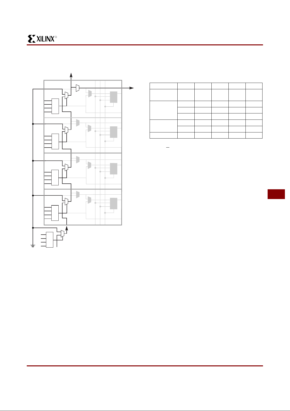
Carry Function
The XC5200 family supports a carry-logic feature that
enhances the performance of arithmetic functions such as
counters, adders, etc. A c arry m ultiplexe r (CY_ MUX) symbol is used to i ndicate the XC5200 carry logic. This symbol
represents the dedicated 2:1 multiplexer in each LC that
performs the one-bit high-speed carry propagate per logic
cell (four bits per CLB).
While the carry propagate is performed inside the LC, an
adjacent LC must be used to complete the arithmetic function. Figure 6 represents an example of an adder function.
The carry propagate is performed on the CLB shown,
which also generat es the hal f-sum fo r the four -bit ad der . An
adjacent CLB is responsible fo r XORing the half-sum with
the corresponding carry-out. Thus an adder or counter
requires two LCs per bit. Notice that the carry chain
requires an initialization stage, which the XC5200 family
accomplishes using the carry initialize (CY_INIT) macro
and one additional LC. The carry chain can propagate vertically up a column of CLBs.
The XC5200 library contains a set of Relationally-Placed
Macros (RPMs) and arithmetic func tions designed to take
advantage of the dedicated carry logic. Using and modifying these macros m akes it much easie r to implement cus-
Figure 6: XC5200 CY_MUX Used for Adder Carry Propagate
F4
F3
F2
F1
F4
F3
F2
F1
F4
F3
F2
F1
F4
F3
F2
F1
XOR
XOR
XOR
XOR
F=0
DI
DI
DI
DI
FD
FD
FD
FD
carry out
carry3
DO
D
X
LC3
DO
DQ
LC2
X
CI
carry in
CY_MUX
CY_MUX
CY_MUX
CY_MUX
CY_MUX
X
DO
DO
DO
DO
LC1
LC0
CKCE CLR
D
D
Q
Q
X
Q
half sum0
carry0
half sum2
half sum1
carry1
carry2
half sum3
CO
A3
or
B3
A3 and B3
to any two
A2 and B2
to any two
A2
or
B2
A1
or
B1
A1 and B1
to any two
A0
or
B0
A0 and B0
to any two
0
F4
F3
F2
F1
F4
F3
F2
F1
F4
F3
F2
F1
F4
F3
F2
F1
XOR
XOR
XOR
XOR
DI
DI
DI
DI
FD
FD
DO
FD
FD
D
X
LC3
DO
DQ
LC2
X
CI
X
LC1
LC0
CK
CE CLR
D
D
Q
Q
X
Q
sum0
sum2
sum1
sum3
CO
Initialization of
carry chain (One Logic Cell)
X5709
R
November 5, 1998 (Version 5.2) 7-89
XC5200 Series Field Programmable Gate Arrays
7
tomized RPMs, freeing the designer from the need to
become an expert on architectures.
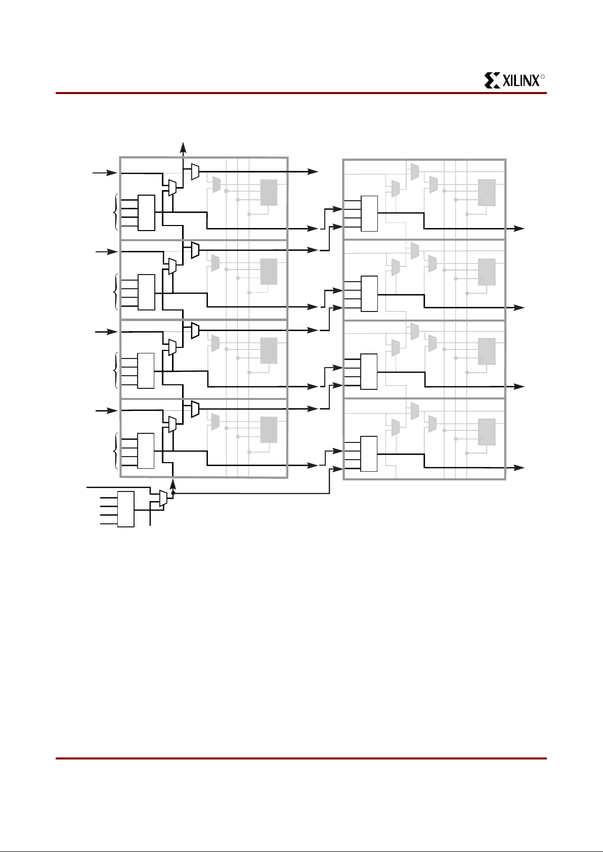
Cascade Function
Each CY_MUX can be connected to the CY_MUX in the
adjacent LC to provide cascadable decode logic. Figure 7
illustrates how the 4- input func tion gener ator s can be configured to take advantage of these four cascaded
CY_MUXes. Note th at AND and OR ca sca ding are sp eci fic
cases of a general decode. In AND cascading all bits are
decoded equal to logic one, while in OR cascading all bits
are decoded equ al to logic zero . The flexibility of the LUT
achieves this result. The XC5200 library contains gate
macros designed to take advantage of this function.
CLB Flip-Flops and Latches
The CLB can pass the combinatorial output(s) to the interconnect network, but can also store the combinatorial
results or other incoming data in flip-flops, and connect
their outputs to the interconnect network as well. The CLB
storage elements can also be configured as latches.
Data Inputs and Outputs
The source of a storage element data input is programmable. It is driven by the function F, or by the Direct In (DI)
block input. The flip-flops or latches drive the Q CLB outputs.
Four fast feed-through paths from DI to DO are available,
as shown in Figure 4. This bypass is sometimes used by
the automated router to repower internal signals. In addition to the storage element (Q) and direct (DO) outputs,
there is a combinatorial output (X) that is always sourced
by the Lookup Table.
The four edge-triggered D-type flip-flops or level-sensitive
latches have common clock (CK) and clock enable (CE)
inputs. Any of the clock inputs can also be permanently
enabled. Storage element functionality is described in
Table 3.
Clock Input
The flip-flops ca n b e trigg er ed o n e ith er th e risin g or fa lling
clock edge. The clock pin is shared by all four storage elements with individual polarity control. Any inverter placed
on the clock input is automatically absorbed into the CLB.
Clock Enable
The clock enable sign al (CE) is active High. The CE pin is
shared by the four storage elements. If left unconnected
for any, the clock enable for that storage element defaults
to the active state. CE is not invertible within the CLB.
Clear
An asynchrono us st orage ele ment i nput ( CLR) ca n be us ed
to reset all four flip- flops or latches in t he CLB. This input
Figure 7: XC 5200 CY_MU X Used f or Decoder Cascade
Logic
F4
F3
F2
F1
F4
F3
F2
F1
F4
F3
F2
F1
F4
F3
F2
F1
A15
A14
A13
A12
A11
A10
A9
A8
A7
A6
A5
A4
A3
A2
A1
A0
AND
AND
F=0
DI
DI
DI
DI
FD
FD
FD
cascade out
out
DO
D
X
LC3
DO
DO
DO
DQ
LC2
X
CI
cascade in
CY_MUX
CY_MUX
CY_MUX
CY_MUX
CY_MUX
FD
X
LC1
Initialization of
carry chain (One Logic Cell)
LC0
CK
CE CLR
DDQ
Q
X
Q
CO
AND
AND
X5708
Table 3: CLB Storage Element Functionality
(active rising edge is shown)
Mode CK CE CLR D Q
Power-Up or
GR
XXXX0
Flip-Flop
XX1X0
__/
1* 0* D D
0X0*XQ
Latch
11*0*XQ
01*0*DD
Both X 0 0* X Q
Legend:
X
__/
0*
1*
Don’t care
Rising edge
Input is Low or unconnected (default value)
Input is High or unconnected (default value)
R
XC5200 Series Field Programmable Gate Arrays
7-90 November 5, 1998 (Version 5.2)
can also be indep en dentl y dis ab led f or any fli p -f lop . C LR i s
active High. It is not invertible within the CLB.
Global Reset
A separate Global Reset line clears each storage element
during power-up, reconfiguration, or when a dedicated
Reset net is driven active. This global net (GR) does not
compete with other routing resources; it uses a dedicated
distribution networ k.
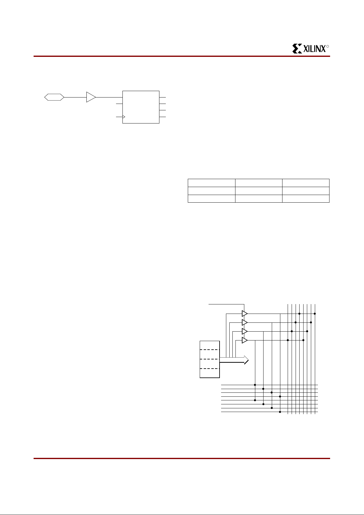
GR can be driven from any user-programmable pin as a
global reset input. To use this global net, place an input pad
and input buffer in the schematic or HDL code, driving the
GR pin of the STARTUP symbol. (See Figure 9.) A specific
pin location can be assigned to this input using a LOC
attribute or property, just as with any other user-programmable pad. An inverter can optionally be inserted after the
input buffer to invert the sense of the Global Reset signal.
Alternativ ely, GR can be driven from any internal node.
Using FPGA Flip-Flops and Latches
The abundance of flip-flops in the XC5200 Series invites
pipelined desi gns. Thi s is a po werful way of i ncreas ing per formance by breaking the function into smaller subfunctions and executing them in parallel, pa ssing on the results
through pipe li ne f li p- fl ops . This me th od shoul d be se rio us l y
considered wherever throughput is more important than
latency.
To include a CLB flip-flop, place the appropriate library
symbol. For example, FDCE i s a D-t y pe fl ip-f l o p wit h cl ock
enable and asynchronous clear. The corresponding latch
symbol is called LDCE.
In XC5200-Series devices, the flip-flops can be used as
registers or shift registers without blocking the function
generators from performing a different, perhaps unrelated
task. This ability increases the functional capacity of the
devices.
The CLB setup time is specified between the function generator inputs and the clock input CK. Therefore, the specified CLB flip-flop setup time includes the delay through the
function generator.
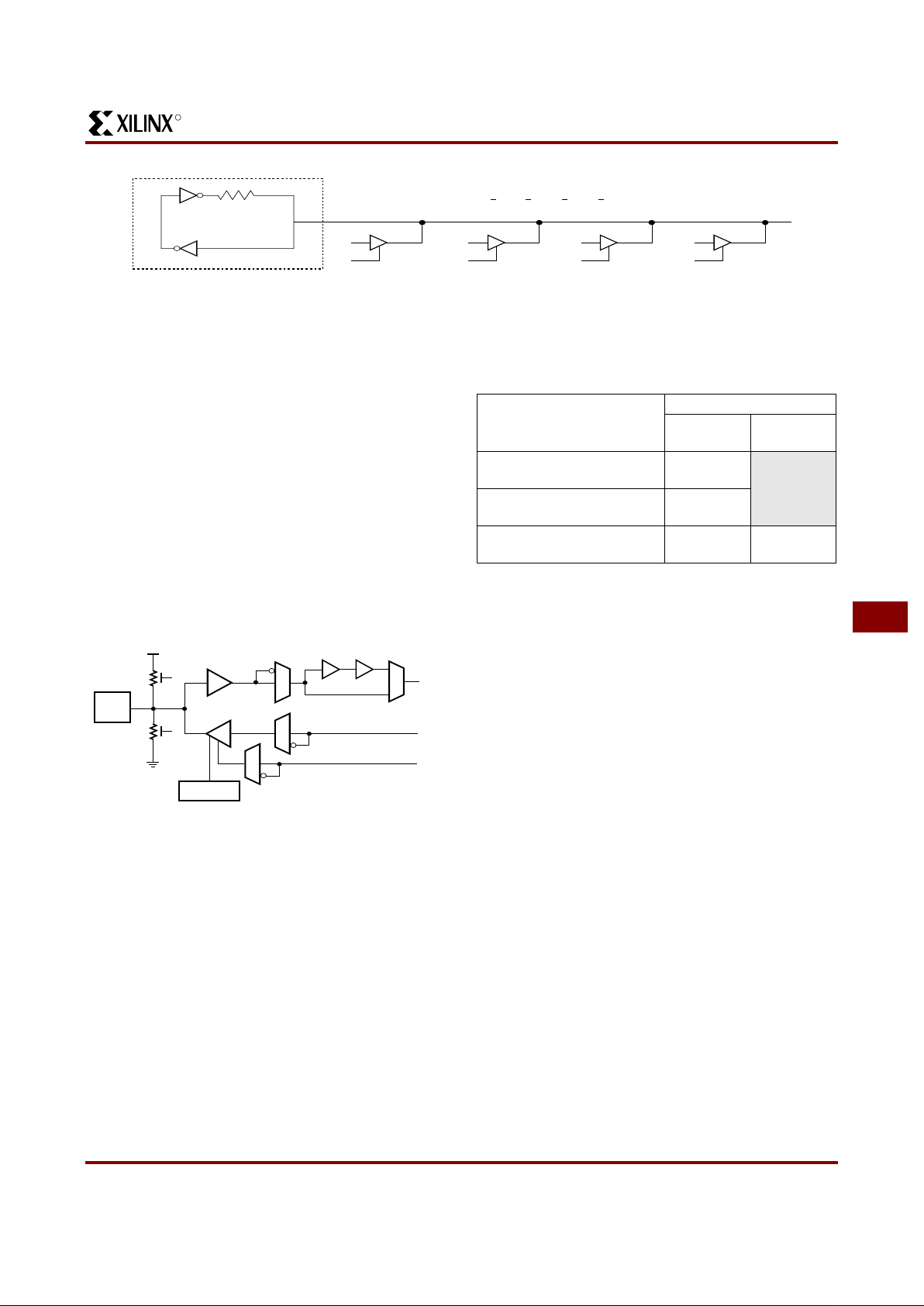
Three-State Buffers
The XC5200 family has four dedicated Three-State Buffers
(TBUFs, or BUFTs in the sche matic library) per CLB (see
Figure 9). The four buffers are individually configurable
through four configuration bits to operate as simple
non-inverting buffers or in 3-state mode. When in 3-state
mode the CLB output enable (TS) control signal drives the
enable to all four buffers. Each TBUF can drive up to two
horizontal an d/or two vertic al Lon glines . These 3- state buf fers can be used to implement multiplexed or bidirectional
buses on the horizontal or vertical longlines, saving logic
resources.
The 3-state buffer e nable is an active -High 3-sta te (i.e. an
active-Low enable), as shown in Table 4.
Another 3-stat e buffer with similar ac cess is located near
each I/O block along the right and left edges of the array .
The longlines driven by the 3-state buffers have a weak
keeper at each end. This circuit prevents undefined floating levels. However, it is overridden by any driver. To
ensure the lon glin e go es high when no bu ffers ar e on , a dd
an additional BUFT to drive the out put Hig h duri ng all of t he
previously undefined states.
Figure 10 shows how to use the 3-state buffers to imple-
ment a multiplexer. The selection is acco mplished by the
buffer 3-state signal.
PAD
IBUF
GR
GTS
CLK
DONEIN
Q1Q4
Q2
Q3
STARTUP
X9009
Figure 8: Schematic Symbols for Global Reset
Table 4: Three-State Buffer Functionality
IN T OUT
X1Z
IN 0 IN
CLB
TS
LC3
LC2
LC1
LC0
CLB
Horizontal
Longlines
X9030
Figure 9: XC5200 3-St ate Buffers
R
November 5, 1998 (Version 5.2) 7-91
XC5200 Series Field Programmable Gate Arrays
7
Input/Output Blocks
User-configurable input/output blocks (IOBs) provide the
interface betwee n external package pins and the intern al
logic. Each IOB controls one packa ge pin and can be configured for input, output, or bidirectional signals.
The I/O block, shown in Figure 11, consists of an input
buffer and an output buffer. The output driver is an 8-mA
full-rail CMOS buffer with 3-state control. Two slew-rate
control modes are supported to minimize bus transients.
Both the out put bu ffer and the 3-state cont ro l a re i n ve rt ibl e .
The input buffer has globally selected CMOS or TTL input
thresholds. T he input bu ffer is invertib le and also provides a
programmable delay line to assure reliable chip-to-chip
set-up and hold times. Minimum ESD protec tion is 3 KV
using the Human Body Model.
IOB Input Signals
The XC5200 inputs can be globally configured for either
TTL (1.2V) or CMOS thresholds, using an option in the bitstream generat ion software. There is a slight hysteresis of
about 300mV.
The inputs of XC5200-Series 5-Volt devices can be driven
by the outputs o f any 3.3-Volt device, if the 5-V olt inputs are
in TTL mode.
Supported sources for XC5200-Series device inputs are
shown in Table 5.
Optional Delay Guarantees Zero Hold Time
XC5200 devices do no t have st orage el ements in the IOBs.
However, XC5200 IOBs can be efficiently routed to CLB
flip-flops o r latches to store the I/O signals.
The data input to th e re gister can o ption ally be d elaye d by
several nanoseconds. With the delay enabled, the setup
time of the input flip -flop is increa sed so that n ormal clock
routing does not result in a positive hold-time requirement.
A positive hold time requirement can lead to unreliable,
temperature- or processing-dependent operation.
The input flip-flop setup time is defined between the data
measured at the de vice I/O pin and the clock inpu t at the
CLB (not at the clock pin). Any routing delay from the
device clock pin to the clock input of the CLB must, therefore, be subtracted from t h is setup time to arrive at t he real
setup time requirement relative to the device pins. A short
specified setup time might, therefore, result in a negative
setup time at the device pins, i.e., a positive hold-time
requirement.
When a delay is i nser t ed on th e data l ine , mor e c loc k de l ay
can be tolerated without causing a positive hold-time
requirement. Sufficient dela y eliminat es the poss ibility of a
data hold-time requirement at the external pin. The maximum delay is therefore inserted as the software default.
The XC5200 IO B has a one-tap d elay elemen t: either the
delay is insert ed (defau lt), or i t is not. The delay guarante es
a zero hold time with respect to clocks routed through any
of the XC5200 global clock buffers. (See “Global Lines” on
page 96 for a description of the global clock buffers in the
XC5200.) For a shorter input register setup time, with
D
N
D
C
D
B
D
A
ABCN
Z = D
A
• A + DB • B + DC • C + DN • N
~100 k
Ω
"Weak Keeper"
X6466
BUFT BUFT BUFT BUFT
Figure 10: 3-State Buffers Implement a Multiplexer
Figure 11: XC5200 I/O Block
I
O
T
PAD
Vcc
X9001
Input
Buffer
Delay
Pullup
Pulldown
Slew Rate
Control
Output
Buffer
Table 5: Supported Sources for XC5200-Series Device
Inputs
Source
XC5200 Input Mode
5 V,
TTL
5 V,
CMOS
Any device, Vcc = 3.3 V,
CMOS outputs
√
Unreliable
Data
Any device, Vcc = 5 V,
TTL outputs
√
Any device, Vcc = 5 V,
CMOS outputs
√√
R
XC5200 Series Field Programmable Gate Arrays
7-92 November 5, 1998 (Version 5.2)
non-zero hold, attach a NODELAY attribute or property to
the flip-flop or input buffer.
IOB Output Signals
Output signals can be optionally inverted within the IOB,
and pass directly to the pad. As with the inputs, a CLB
flip-flop or latch can be used to store the output si gnal.
An active-High 3-state signal can be used to plac e the output buffer in a high-impedance state, implementing 3-state
outputs or bidirectional I/O. Under configuration control,
the output (OUT) and output 3-state (T) signals can be
inverted. The polarity of these signals is independently
configured for each IOB.
The XC5200 devi ces p rovid e a gua rant eed out put sink c urrent of 8 mA.
Supported destinations for XC5200-Series device outputs
are shown in Table 6.(For a detailed disc ussion of how to
interface between 5 V and 3.3 V devices, see the 3V Products section of
The Programmable Logic Data Book
.)
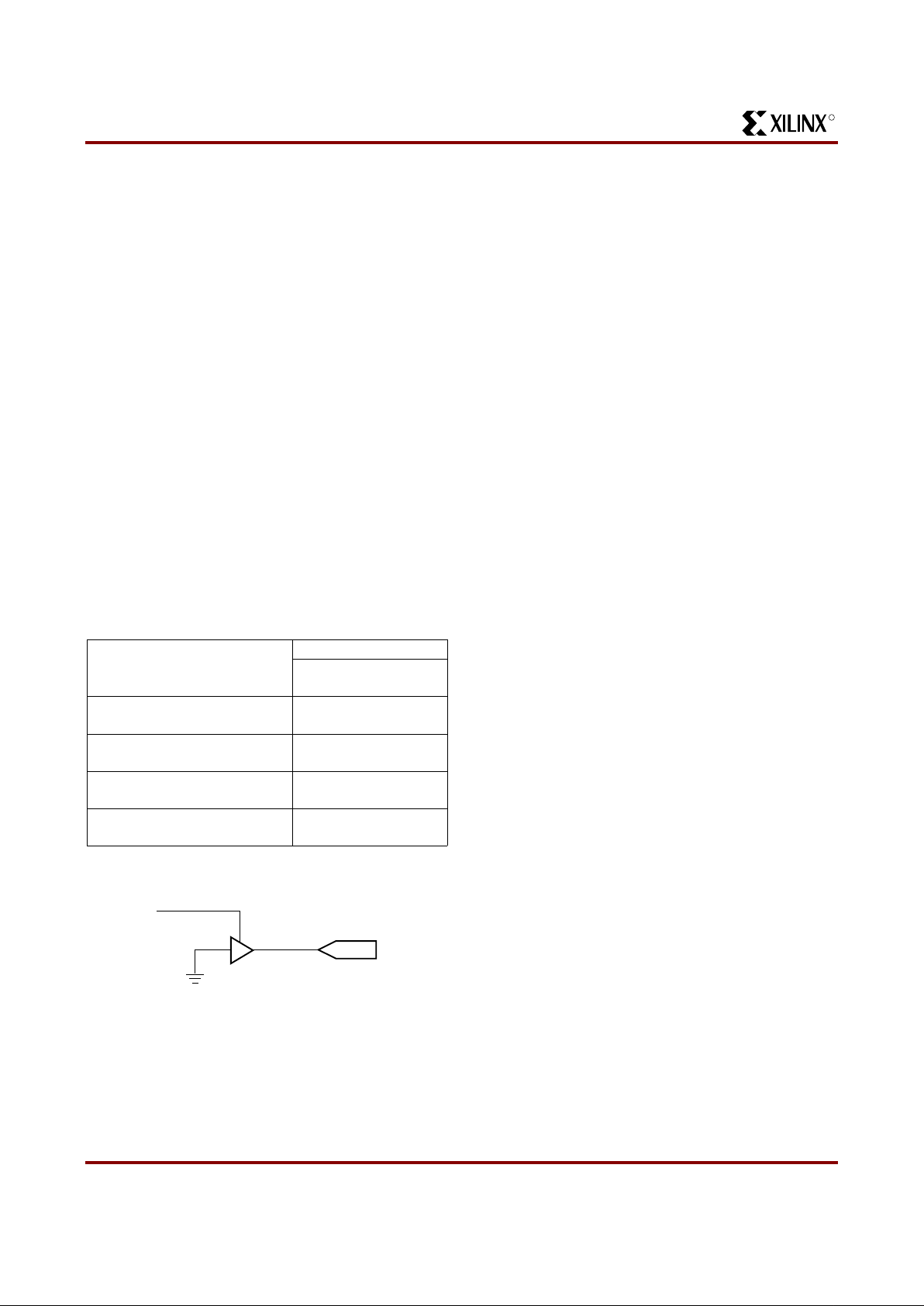
An output can be co nfigu red as ope n-dr ain (open -coll ect or)
by placing an OBUFT symbol in a schematic or HDL code,
then tying the 3-state pin (T) to the output signal, and the
input pin (I) to Ground. (See Figure12.)
Table 6: Supported Destinations for XC520 0-Series
Outputs
Output Slew Rate
The slew rate of each output buffer is, by default, reduced,
to minimize power bus tran sient s when sw itching no n-cr itical signals. For critical sig nals, attach a FAST attribute or
property to the output buffer or flip-flop.
For XC5200 devices, maximum total capacitive load for
simultaneous fast mo de switching in the sam e direction is
200 pF for all packag e pins between each P ower/Ground
pin pair. For some XC5200 devices, additional internal
Power/Ground pin pairs are connected to special Power
and Ground planes within the packages, to reduce ground
bounce.
For slew-rate limited outputs this total is two times larger for
each device type: 400 pF for XC5200 devices. This maximum capacitive load should not be exceeded, as it can
result in ground bounce of grea ter than 1. 5 V amplitud e and
more than 5 ns duration. This level of ground bounce may
cause undesired transient behavior on an output, or in the
internal logic. This r estriction is comm on to all high-spe ed
digital ICs, and is not particular to Xilinx or the XC5200
Series.
XC5200-Series devices have a feature called “Soft
Start-up,” de signed to red uce gr ound bo unce when al l outputs are turned on simultaneously at the end of configuration. When the configuration process is finished and the
device starts up, the first activation of the outputs is automatically slew-rate limited. Immediately following the initial
activation of the I/O, the slew rate of the individual outputs
is determined by the individual configuration option for
each IOB.
Global Three-State
A separate Global 3-State line (not shown in Figure 11)
forces all FPGA outputs to the high-impedance state,
unless boundary scan is enabled and is executing an
EXTEST instruction. This global net (GTS) does not compete with othe r rou ting r esou rces ; it u ses a dedic ate d dist ribution network.
GTS can be driven from any user-programmable pin as a
global 3-state input. To use this global net, place an input
pad and input buffer in the schematic or HDL code, driving
the GTS pin of the STARTUP symbol. A specific pin location can be assigned to this input using a LOC attribute or
property , just as wi th any ot her us er-prog rammable p ad. An
inverter can optionally be inserted after the input buffer to
invert the sens e of the Gl obal 3-S tate si gnal. Us ing GTS is
similar to Global Reset. See Figure 8 on page 90 for
details. Alternatively, GTS can be driven from any internal
node.
Other IOB Options
There are a number of other programmable options in the
XC5200-Series IOB.
Pull-up and Pull-down Resist ors
Programmable IOB pull-up and pull-down resistors are
useful for tying unused pins to Vcc or Ground to minimize
power consumption and reduce noise sensitivity. The configurable pull-up resistor is a p-channel transistor that pulls
Destination
XC5200 Output Mode
5 V,
CMOS
XC5200 device, V
CC
=3.3 V,
CMOS-threshold inputs
√
Any typical devi ce, V
CC
= 3.3 V,
CMOS-threshold inputs
some
1
1. Only if destination device has 5-V tolerant inp uts
Any device, VCC = 5 V,
TTL-threshold inputs
√
Any device, V
CC
= 5 V,
CMOS-threshold inputs
√
X6702
OPAD
OBUFT
Figure 12: Open-Drain Output
R
November 5, 1998 (Version 5.2) 7-93
XC5200 Series Field Programmable Gate Arrays
7
to Vcc. The confi gurabl e pull-d own resi stor is an n-chan nel
transistor that pulls to Ground.
The value of these resistors is 20 kΩ − 100 kΩ. This high
value makes them unsuit able as wired-AND pull-u p resistors.
The pull-up resi stors f or most u ser-pr ogrammabl e IOBs ar e
active during the configuration process. See Table 13 on
page 124 for a list of pins with pull-ups active before and
during configuration.
After configuration, voltage levels of unused pads, bonded
or unbonded, must be valid logic levels, to reduce noise
sensitivity and avoid excess current. Therefore, by default,
unused pads are configured with the internal pull-up resistor active. Alternatively, they can be individually configured
with the pull-down resistor, or as a driven output, or to be
driven by an external source. To activate the internal
pull-up, attach the PULLUP library component to th e net
attached to the pad. To activate the internal pull-down,
attach the PULLDOWN library component to the net
attached to the pad.
JTAG Support
Embedded logic attached to the IOBs contains test structures compatible with IEEE Standard 1149.1 for boundary
scan testing, simplifying board-level testing. More information is provided in “Boundary Scan” on page 98.
Oscillator
XC5200 devices include a n internal os cillator. This oscillator is used to clock the powe r-on tim e-ou t, cl ear co nfigur ation memory, and source CCLK in Master configuration
modes. The oscillator runs at a nominal 12 MHz frequ en cy
that varies with process, Vcc, and temperature. The output
CCLK frequency is selectable as 1 MHz (default), 6 MHz,
or 12 MHz.
The XC5200 oscillator divides the internal 12-MHz clock or
a user clock. The user then has the choice of dividing by 4,
16, 64, or 256 for the “OSC1” output and dividing by 2, 8,
32, 128, 1024, 4096, 16384, or 65536 for the “OSC2” output. The division is specified via a “DIVIDEn_BY=x”
attribute on the symbol, where n=1 for OSC1, or n=2 for
OSC2. These frequencies can vary by as much as -50% or
+ 50%.
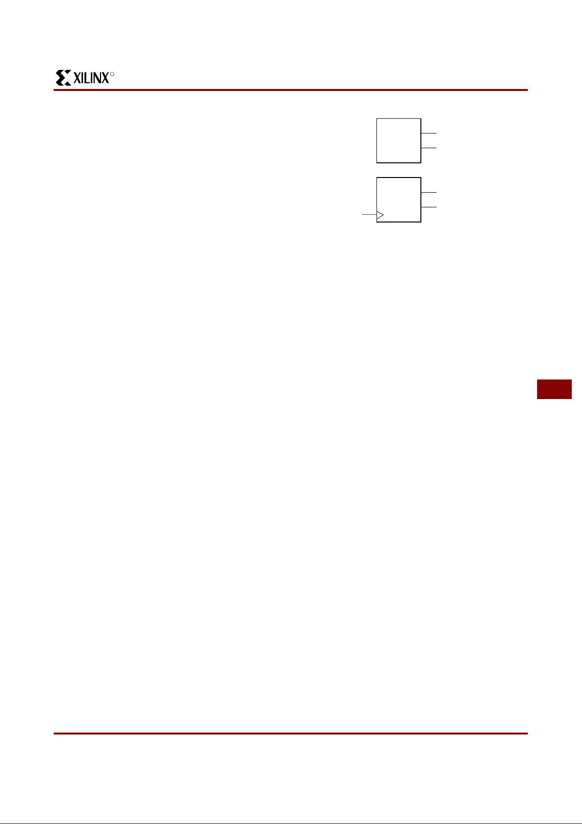
The OSC5 macro is used where an internal oscillator is
required. The CK_DIV macro is applicable when a user
clock input is specified (see Figure 13).
VersaBlock Routing
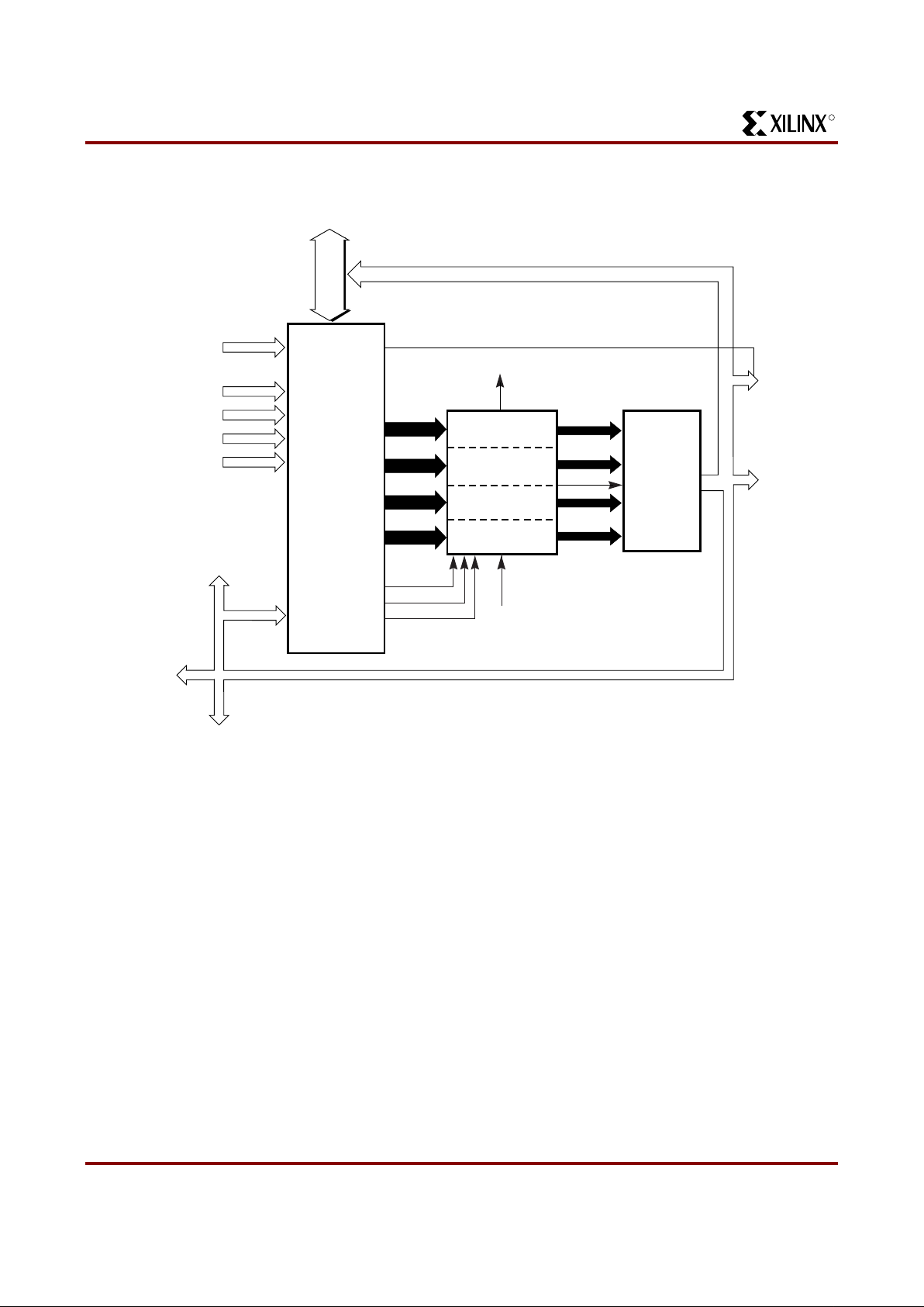
The General Routing Matrix (GRM) connects to the
Versa-Block via 24 bidirectional ports (M0-M23). Excluding
direct connections, global nets, and 3-statable Longlines,
all VersaBlock i np uts an d ou tp ut s conne ct to th e GRM v i a
these 24 ports. Four 3-statable unidirectional signals
(TQ0-TQ3) drive out of the VersaBlock directly onto the
horizontal and vertical Longlines. Two horizontal global
nets and two vertical global nets connect directly to every
CLB clock pin; the y can conn ect to other CLB input s via the
GRM. Each CLB also has four unidirectional direct connects to each of its four neighboring CLBs. These direct
connects can also feed directly back to the CLB (see
Figure 14).
In addition, ea ch C LB ha s 1 6 dir ec t in p ut s, fo ur d i re ct co n nections from each of the neighboring CLBs. These direct
connections provide high-speed local routing that
bypasses the GRM.
Local Interconnect Matrix
The Local Inter connect M atrix (L IM) is built from in put and
output multiplexers. The 13 CLB outputs (12 LC outputs
plus a V
cc
/GND signal) connect to the eight VersaBlock
outputs via the output multiplexers, which consist of eight
fully populated 13-to-1 multiplexers. Of the eight
VersaBlock outputs, four signals drive each neighboring
CLB directly, and provide a dire ct feedba ck path to the input
multiplexers. The four remaining multiplexer outputs can
drive the GRM through four TBUFs (TQ0-TQ3). All eight
multiplexer outputs can connect to the GRM through the
bidirectiona l M0- M23 s ign al s. A ll eigh t s igna l s a l so con ne ct
to the input multiplexers and are potential inputs to that
CLB.
OSCS
CK_DIV
OSC1
OSC1
OSC2
OSC2
5200_14
Figure 13: XC5200 Oscillator Macros
R
XC5200 Series Field Programmable Gate Arrays
7-94 November 5, 1998 (Version 5.2)
CLB inputs have several possible sources: the 24 signals
from the GRM, 16 direct connections from neighboring
VersaBlocks, four signals from global, low-skew buffers,
and the four signals from the CLB output multiplexers.
Unlike the output multiplexers, the input multip lexers are
not fully populated; i.e., only a subset of the available signals can be con nected to a give n CLB in put. The fle xibility
of LUT input swapping and LUT mapping compensates for
this limitation. For example, if a 2-input NAND gate is
required, it can be mapped into any of the four LUTs, and
use any two of the four inputs to the LUT.
Direct Connects
The unidirectional direct-connect segments are connected
to the logic input/output pins through the CLB input and output multiple xe r ar rays , and th us bypa ss t he g enera l rou t ing
matrix altogether. These lines increase the routing channel
utilization, while simultaneously reducing the delay
incurred in speed-critical connections.
The direct connects also provide a high-speed path from
the edge CLBs to the VersaRing input/output buffers, and
thus reduce pin-to-pin set-up time, clock-to-out, and combinational propag ation delay. Direct connects from the input
buffers to the CLB DI pin (direct flip-flop input) are only
available on the left and right edges of the device. CLB
look-up table inputs and combinatorial/registered outputs
have direct connects to input/output buffers on all four
sides.
The direct connects are ideal for developing customized
RPM cells. Using direct connects improves the macro performance, and leaves the other routing channels intact for
improved routing. Direct connects can also route through a
CLB using one of the four cell-feedthrough paths.
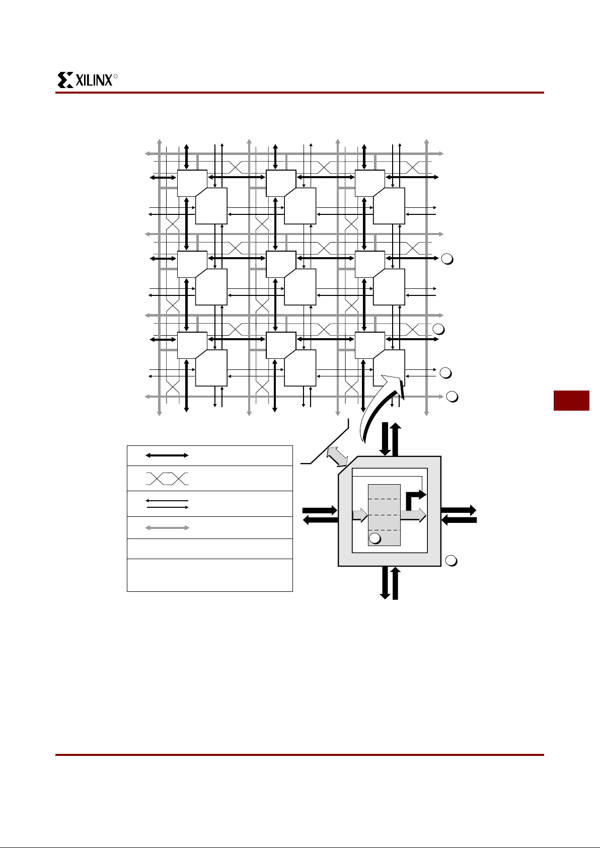
General Routing Matrix
The General R outing Matrix, shown in Figure 15, provide s
flexible bidirectio nal connect ions to th e Local Int erconnect
Figure 14: VersaBlock Details
4
4
4
4
5
5
5
5
3
3
3
3
24
To GRM
M0-M23
CLB
CLK
Direct North
Direct to
East
To
Longlines
and GRM
TQ0-TQ3
Global Nets
Feedback
Direct West
Direct South
CE
CLR
C
IN
C
OUT
V
CC
/GND
TS
4
4
North
4
8
South
4
East
4
West
4
LC3
LC2
LC1
LC0
Output
Multiplexers
Input
Multiplexers
8
4
4
4
X5724
R
November 5, 1998 (Version 5.2) 7-95
XC5200 Series Field Programmable Gate Arrays
7
Matrix through a hierarchy of different-length metal segments in both the horizontal and vertical directions. A pro-
grammable interconnect point (PIP) establishes an electrical connection between two wire segments. The PIP, consisting of a pass transisto r switch controlled by a memo ry
element, provides bidirectional (in some cases, unidirectional) connection between two adjoining wires. A collection of PIPs inside the General Routing Matrix and in the
Local Interconnect Matrix provides connectivity between
various types of metal segments. A hierarchy of PIPs and
associated routing segments combine to provide a powerful interconnect hierarchy:
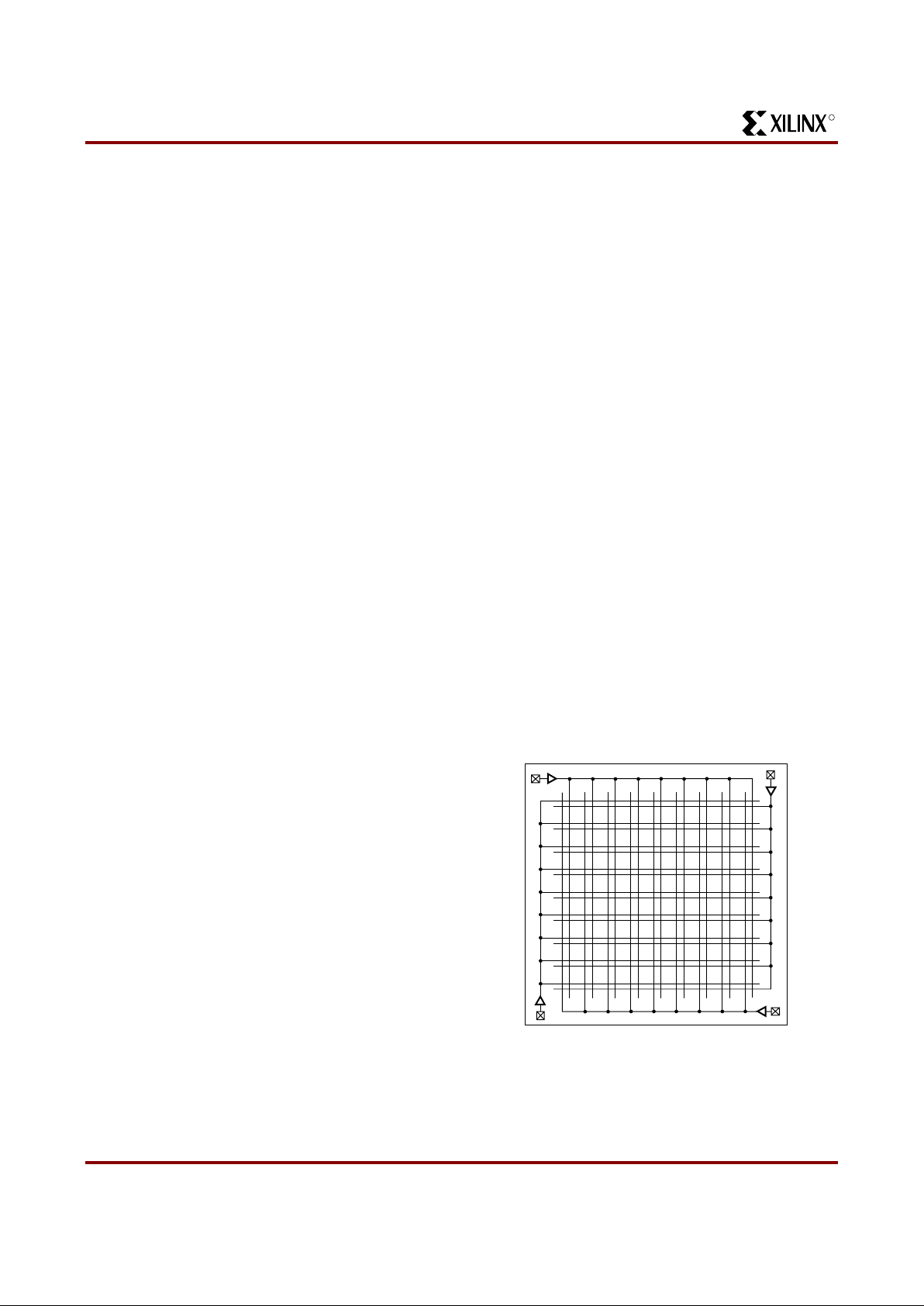
• Forty bidirectional single-length segments per CLB
provide ten routing channels to each of the four
neighboring CLBs in four directions.
• Sixteen bi directional double-length segme nts per CLB
provide four routing channels to each of four other
(non-neighbor ing ) CL B s in four dir ec tio ns .
• Eight horizontal and eight vertical bidirectional Longline
Figure 15: XC5200 Interconnect Structure
X4963
Versa-
Block
GRM
Single-length Lines
Double-length Lines
Direct Connects
Longlines and Global Lines
1
Six Levels of Routing Hierarchy
1
2
3
4
5
2
3
4
Versa-
Block
GRM
Versa-
Block
GRM
Versa-
Block
GRM
Versa-
Block
GRM
Versa-
Block
GRM
Versa-
Block
GRM
Versa-
Block
GRM
Versa-
Block
GRM
Local Interconnect Matrix
Logic Cell Feedthrough
Path (Contained within each
Logic Cell)
LIM5
6
CLB
Direct Connects
TS
LIM
4
4
4
4
4
LC3
LC2
LC1
LC0
44
44
24
24
6
GRM
R
XC5200 Series Field Programmable Gate Arrays
7-96 November 5, 1998 (Version 5.2)
segments span the width and height of the chip,
respectively.
Two low-skew horizontal and vertical unidirectional global-line segments sp an each row and co lumn of the chip,
respectively.
Single- and Double-Length Lines
The single- and double-length bidirectional line segments
make up the bulk of the routing channels. The double-length lines hop across every other CLB to reduce the
propagation del ays i n spe ed-cri tic al net s. Rege nerat ing the
signal strength is recommended after traversing three or
four such segm ents. Xilinx place-an d-route software a utomatically connects buffers in the path of the signal as necessary. Single- and double-lengt h lines cannot drive onto
Longlines and global lines; Longlines and global lines can,
however, drive onto single- and double-length lines. As a
general rule, Longline and global-line connections to the
general routing matrix are unidirectional, with the signal
direction fr om these lines toward the routing matrix.
Longlines
Longlines ar e used f or hig h-fan-out signal s, 3 -state b usses,
low-skew nets, and faraway destinations. Row and column
splitter PIP s in the middl e of the ar ray ef fecti vely doub le the
total number of Longlines by electrically dividing them into
two separated half-lines. Longlines are driven by the
3-state buffers in ea ch CLB, and are driv en by si m ilar bu ffers at the periphery of the array from the VersaRing I/O
Interface.
Bus-oriented design s are e asily implemen ted by using Longlines in conju nctio n wi th t he 3 -st ate buf fers in the CLB a nd
in the VersaRing. Additionally, weak keeper cells at the
periphery reta in the last valid logic level on the Longlin es
when all buffers are in 3-stat e mode.
Longlines connect to the single-length or double-length
lines, or to the logic inside the CLB, through the General
Routing Matrix. The only manner in which a Longline can
be driven is through the four 3-state buffers; therefore, a
Longline-to-Longline or single-line-to-Longline connection
through PIPs in the General Routing Matrix is not possible.
Again, as a general rule, long- and global-line connections
to the General Routing Matrix are unidirectional, with the
signal direction from these lines toward the routing matrix.
The XC5200 famil y h as no p ull -ups o n t he ends o f the Lon glines sourced by TBUFs, unlike the XC4000 Series. Consequently, wired functions (i . e. , WAND and WORAND) and
wide multiplexing functions requiring pull-ups for undefined
states (i.e ., b us ap pli cat i on s) mus t be imp l eme nted i n a dif ferent way. In the case of the wired functions, the same
functionality can be achieved by taking advantage of the
carry/cascade logic described above, implementing a wide
logic function in p lace of the wired func tion. In the c ase of
3-state bus a pplicat ions, t he user must in sure th at all s tates
of the multiplexing function are defined. This process is as
simple as adding an additional TBUF to drive the bus High
when the previously undefined states are activated.
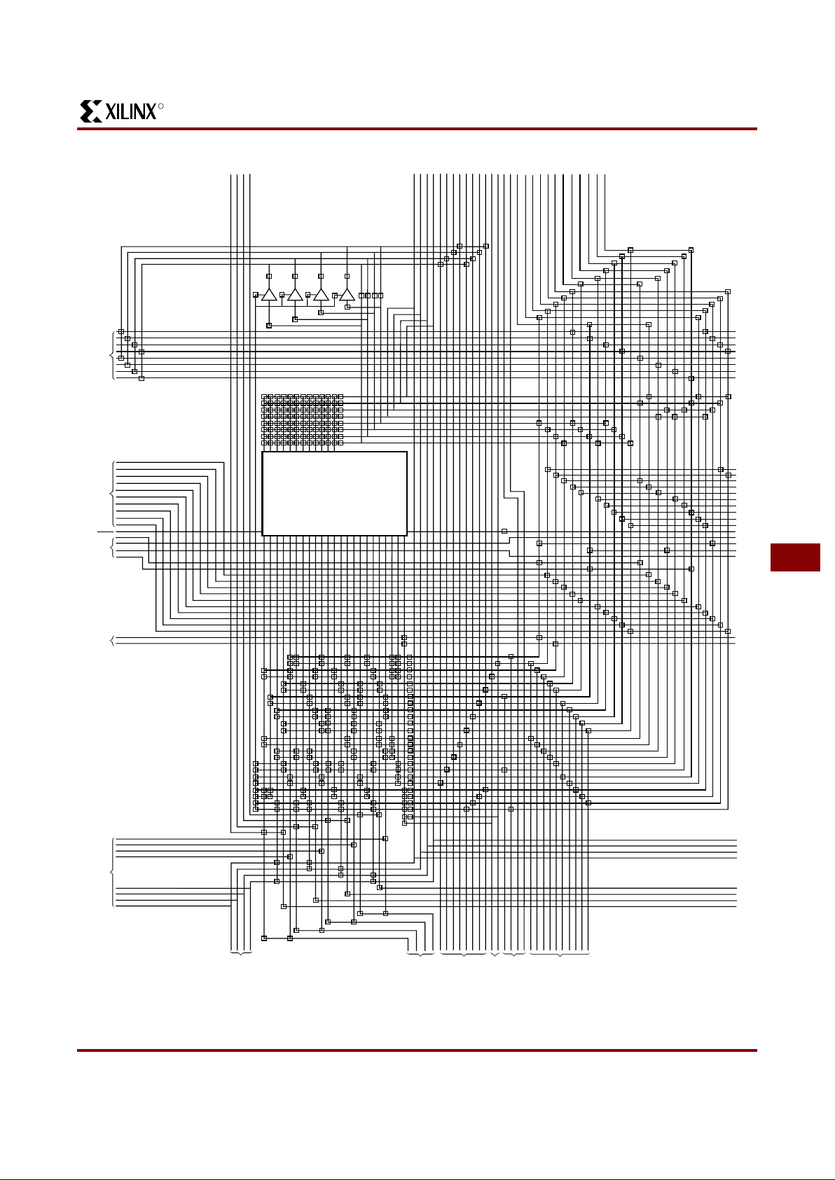
Global Lines
Global buffers in Xilinx FPGAs are special buffers that drive
a dedicated routing network called Global Lines, as shown
in Figure16. This network is intended for high-fanout
clocks or other c ontrol signals , to maxim ize spe ed and minimize skewing while distributing the signal to many loads.
The XC5200 family has a total of four global buffers (BUFG
symbol in the library), each with its own dedicated routing
channel. Two are distributed vertically and two horizontally
throughout the FPGA.
The global lines provide direct input only to the CLB clock
pins. The global lines also connect to the General Routing
Matrix to provide ac cess from these lines to the function
generators and other control signals.
Four clock input pads at the corners of the chip, as shown
in Figure16, provide a high-spe ed, low- skew c lock net work
to each of the four global-line buffers. In addition to the dedicated pad, the global lines can be sourced by internal
logic. PIPs from several routing channels within the VersaRing can also be configured to drive the global-line buffers.
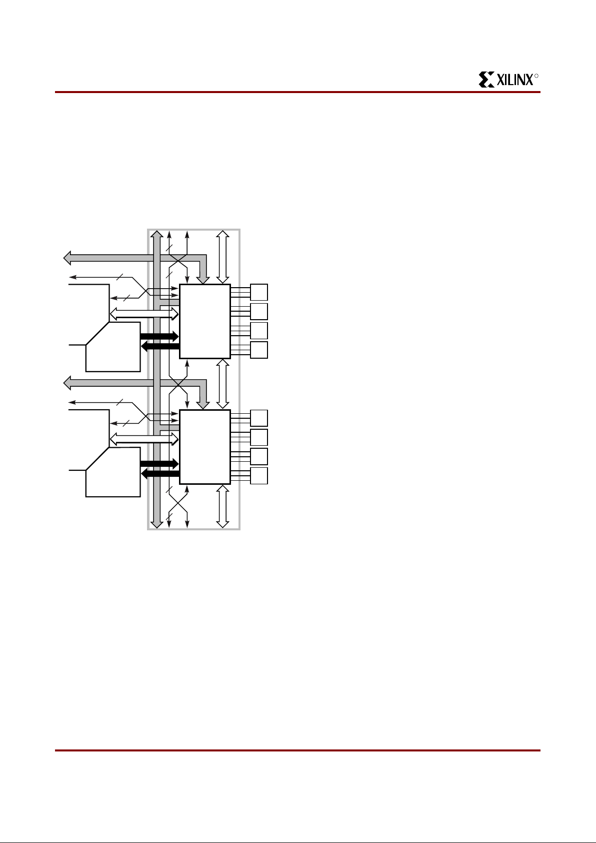
Details of all the programmable interconnect for a CLB is
shown in Figure 17.
Figure 16: Global Lines
GCK1
GCK4
GCK3
GCK2
X5704
R
November 5, 1998 (Version 5.2) 7-97
XC5200 Series Field Programmable Gate Arrays
7
.
CLB
DOUBLEGLOBAL
CARRY
SINGLE LONG
DIRECT
DIRECT
DIRECT
DOUBLE
SINGLE
LONG
GLOBAL
x9010
Figure 17: Detail of Programmable Interconnect Associated with XC5200 Series CLB
R
XC5200 Series Field Programmable Gate Arrays
7-98 November 5, 1998 (Version 5.2)
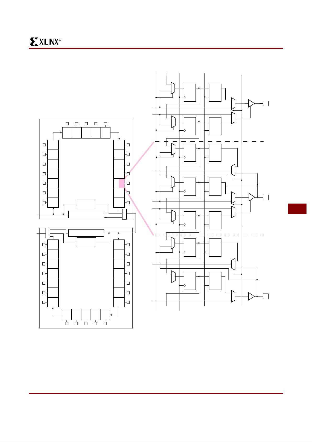
VersaRing Input/Output Interface
The Vers aRing, shown in Figure 18, is positioned between
the core logic and the pad ring; it has all the routing
resources of a VersaBlock without the CLB logic. The VersaRing decouples the core logic from the I/O pads. Each
VersaRing Cell provides up to four pad-cell connections on
one side, and connects directly to the CLB ports on the
other side.
Boundary Scan
The “bed of nails” has been the trad itional method of test ing
electronic assemblies. This approach has become less
appropriate, due to closer pin spacing and more sophisticated assembly methods like surface-mount technology
and multi-layer boards. The IEEE boundary scan standard
1149.1 was developed to facilitate board-level testing of
electronic assemblies. Design and test engineers can
imbed a standard test logic structure in their device to
achieve high fault coverage for I/O and internal logic. This
structure is easily implemented with a four-pin interface on
any boundary sca n-compatib le IC. IEEE 1149.1-compatibl e
devices may be s erial daisy- chaine d toget her , connecte d in
parallel, or a combination of the two.
XC5200 devices support all the mandatory boundary-scan
instructions specified in the IEEE standard 1149.1. A Test
Access Port (TAP) and registers are provided that implement the EXTEST, SAMPLE/PRELOAD, and BYPASS
instructions. The TAP can also s upport two USERCODE
instructions. When the boundary scan configuration option
is selected, three normal user I/O pins become dedicated
inputs for these functions. Another user output pin
becomes the dedicated boundary scan output.
Boundary-scan operation is independent of individual IOB
configuration and package type. All IOBs are treated as
independently controlled bidirectional pins, including any
unbonded IOBs. R etaining the bidirection al test capability
after configura tion provides f lexibility for interconnect te sting.
Also, internal signals can be captured during EXTEST by
connecting them to unbonded IOBs, or to the unused outputs in IOBs used as unidirectional input pins. This technique partially compensates for the lack of INTEST
support.
The user can serially load commands and data into these
devices to control the driving of their outputs and to examine their inputs. This method is an improvement over
bed-of-nails testing. It avoids the need to over-drive device
outputs, and it reduces the user interface to four pins. An
optional fift h pin, a rese t for the c ontrol lo gic, is des cribe d in
the standard but is not implemented in Xilinx devices.
The dedicated on-chip logic implementing the IEEE 1149.1
functions in clu des a 16- st a te machi n e, an ins tr uc t ion r eg i ster and a number of data registers. The functional details
can be found in the IEEE 1149.1 specification and are also
discussed in the Xilinx application note XAPP 017:
“Bound-
ary Scan in XC4000 and XC5200 Series devices”
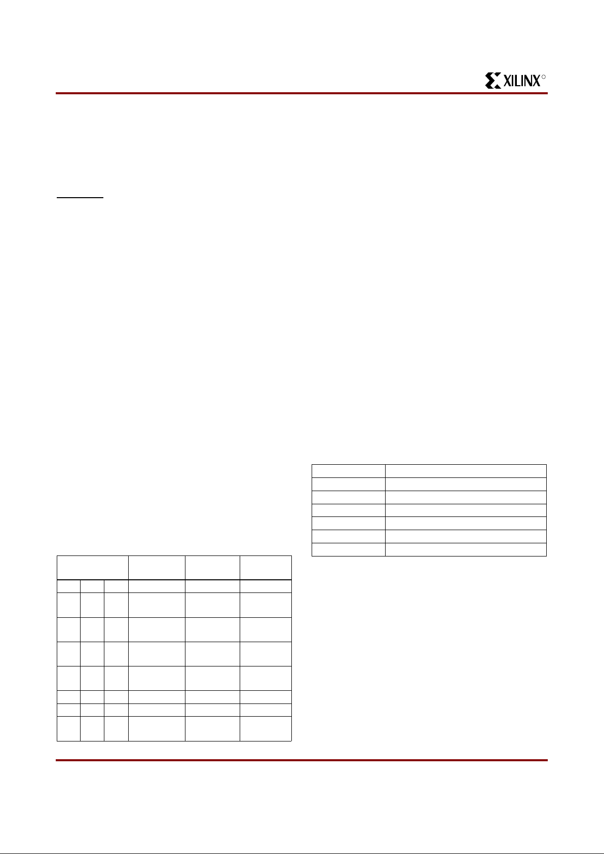
Figure 19 on page 99 is a diagram of the XC5200-Series
boundary scan logic. It includes three bits of Data Register
per IOB, the IEEE 11 49.1 Tes t Access Port controller, and
the Instruct ion Register wit h decodes.
The public boundary-scan instructions are always available
prior to confi guration . Afte r config uration, the pub lic inst ructions and any USERCODE instructions are only available if
specified in the design. While SAMPLE and BYPASS are
available during configuration, it is recommended that
boundary-scan operations not be performed during this
transitory period.
In addition to the test instructions outlined above, the
boundary-sca n circui try can be used t o config ure the FPGA
device, and to r e ad back the configuration data.
All of the XC4000 boundary-scan modes are supported in
the XC5200 family. Three additional outputs for the UserRegister are provided (Reset, Update, and Shift), repre-
Figure 18: VersaRing I/O Interface
8
8
GRM
VersaBlock
8
VersaRing
2
4
8
8
4
4
4
10
2
GRM
VersaBlock
8
2
2
2
2
2
2
8
10
Interconnect
Interconnect
Pad
Pad
Pad
Pad
Pad
Pad
Pad
Pad
X5705
R
November 5, 1998 (Version 5.2) 7-99
XC5200 Series Field Programmable Gate Arrays
7
senting the decoding of the corresponding state of the
boundary-scan internal state machine.
D Q
D Q
D Q
IOB
IOB
IOB
IOB
IOB
IOB
IOB
IOB
IOB
IOB
IOB
IOB
IOB
M
U
X
BYPASS
REGISTER
IOB IOB
TDO
TDI
IOB IOB IOB
M
U
X
TDO
TDI
IOB
IOB
IOB
IOB
IOB
IOB
IOB IOB
IOB
IOB
IOB
IOB
IOB
IOB
IOB IOB IOB IOB IOB
1
0
1
0
1
0
1
0
1
0
1
0
1
0
DQ
LE
sd
sd
LE
DQ
D Q
D Q
1
0
1
0
1
0
1
0
DQ
LE
sd
sd
LE
DQ
sd
LE
DQ
IOB
D Q
D Q
1
0
1
0
DQ
LE
sd
sd
LE
DQ
1
0
DATA IN
IOB.T
IOB.O
IOB.I
IOB.O
IOB.T
IOB.I
IOB.O
SHIFT/
CAPTURE
CLOCK DATA
REGISTER
DATAOUT UPDATE EXTEST
X1523_01
INSTRUCTION REGISTER
INSTRUCTION REGISTER
BYPASS
REGISTER
Figure 19: XC5200-Series Boundary Scan Logic
R
XC5200 Series Field Programmable Gate Arrays
7-100 November 5, 1998 (Version 5.2)
XC5200-Series devi ces c an a lso be conf igu red t hrou gh t he
boundary scan logic. See XAPP 017 for more information.
Data Registers
The primary data register is the boundary scan register.
For each IOB pin in the FPGA, bonded or not, it includes
three bits for In , Out and 3-State Contro l. Non-IOB pins
have appropriat e partial bit population for In or Out only.
PROGRAM
, CCLK and DONE are not included in the
boundary scan register. Each EXTEST CAPTURE-DR
state captures all In, Out, and 3-State pins.
The data register also includes the following non-pin bits:
TDO.T, and TDO.O, which are always bits 0 and 1 of the
data register, respectively, and BSCANT.UPD, which is
always the last bit of the data register. These three boundary scan bits are special-purp ose Xilinx te st sig na ls.
The other standard data register is the single flip-flop
BYPASS register. It synchronizes data being passed
through the FPGA to the next downstream boundary scan
device.
The FPGA provides two additional data regis ters that can
be specified using the BSCAN macro. The FPGA provides
two user pins (BSCAN.SEL1 and BSCAN.SEL2) which are
the decodes of two user ins truction s, USER1 an d USER2.
For these instructions, two corresponding pins
(BSCAN.TDO1 and B SCAN.TDO 2) allow us er scan data to
be shifted out on TDO. The data register clock
(BSCAN.DRCK) is available fo r control of test logic which
the user may wish to implement with CLBs. The NAND of
TCK and RUN-TEST-IDLE is also provided (BSCAN.IDLE).
Instruction Set
The XC5200-Series boundary scan instruction set also
includes instructions t o configure the device and read back
the configuration data. The instruction set is coded as
shown in Table 7.
Table 7: Boundary Scan Instructions
Bit Sequence
The bit sequence within each IOB is: 3-State, Out, In. The
data-register cells for the TAP pins TMS, TCK, and TDI
have an OR-gate that permanently disables the output
buffer if boundary-scan operation is selected. Consequently , it is im possibl e for t he outp uts in IO Bs used b y TAP
inputs to conflict with TAP operation. TAP data is taken
directly from the pin, and cannot be overwritten by injected
boundary-scan data.
The primary global clock inputs (PGCK1-PGCK4) are
taken directly f ro m t he pin s, a nd ca nno t be ov erwr i tte n w it h
boundary-scan data. However, if necessary, it is possible to
drive the clock input from boundary scan. The external
clock source is 3-stated, and the clock net is driven with
boundary scan data through the output driver in the
clock-pad IOB . If t he cloc k-pad I OBs are u sed for non-cl ock
signals, the data may be overwritten normally.
Pull-up and pull-down resistors remain active during
boundary scan. Before and during configuration, all pins
are pulled up. After configuration, the choice of internal
pull-up or pull-down resistor must be taken into account
when designing test vectors to detect open-circuit PC
traces.
From a cavity-up view of the chip (as shown in XDE or
Epic), starting in the upper right chip corner, the boundary
scan data-register bits are ordered as shown in Ta ble 8 .
The device-specific pinout tables for the XC5200 Series
include the boundary scan locations for each IOB pin.
Table 8: Boundary Scan Bit Sequence
BSDL (Boundary Scan Description Language) files for
XC5200-Series devices are available on the Xilinx web site
in the File Download area.
Including Boundary Scan
If boundary scan is o nly to be use d duri ng con fig urat ion, n o
special eleme nts need b e incl uded i n the sch ematic o r HDL
code. In this case, the special boundary scan pins TDI,
TMS, TCK and TDO can be used for user function s after
configuration.
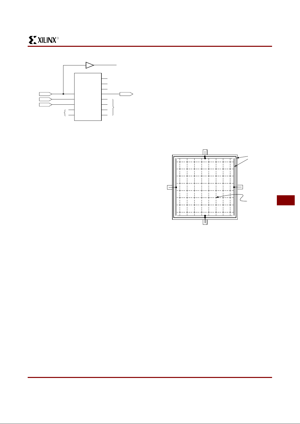
T o in dicate that bou ndary scan remain enable d after conf iguration, incl ude the BSCAN li brary symbol and connect pad
symbols to the TDI, TMS, TCK and TDO pins, as shown in
Figure 20.
Instruction I2
I1 I0
Test
Selected
TDO Source
I/O Data
Source
0 0 0 EXTEST DR DR
0 0 1 SAMPLE/PR
ELOAD
DR Pin/Logic
0 1 0 USER 1 BSCAN.
TDO1
User Logic
0 1 1 USER 2 BSCAN.
TDO2
User Logic
1 0 0 READBACK Readback
Data
Pin/Logic
1 0 1 CONFIGURE DOUT Disabled
1 1 0 Reserved ——
1 1 1 BYPASS Bypass
Register
—
Bit Position I/O Pad Location
Bit 0 (TDO) Top-edge I/O pads (right to left)
Bit 1 ...
... Left-edge I/O pads (top to bottom)
... Bottom-edge I/O pads (left to right)
... Right-edge I/O pads (bottom to top)
Bit N (TDI) BSCANT.UPD
R
November 5, 1998 (Version 5.2) 7-101
XC5200 Series Field Programmable Gate Arrays
7
Even if the boundary scan symbol is used in a schematic,
the input pins TMS, TCK, and TDI can still be used as
inputs to be rout ed to interna l logic. C are must be take n not
to force the chip into an undesired boundary scan state by
inadvertently applying boundary scan input patterns to
these pins. The simplest way to prevent this is to keep
TMS High, and then apply whatever signal is desired to TDI
and TCK.
Avoiding Inadvertent Boundary Scan
If TMS or TCK is used as user I/O, care must be taken to
ensure that at leas t on e of th ese p ins is held co nsta nt du ring configuration. In some applications, a situation may
occur where TMS or TCK is driven during configuration.
This may cause the devi ce to go into boundary scan mode
and disrupt the configuration process.
To prevent activation of boundary scan during configuration, do either of the following:
• TMS: Tie High to put the Test Access Port controller
in a benign RESET state
• TCK: Tie High or Low—do not toggle this cl ock input.
For more information regarding boundary scan, refer to the
Xilinx Application Note XAPP 017, “
Boundary Scan in
XC4000 and XC5200 De vices
.“
Power Distribution
Power for the FPGA is di stri bute d thro ugh a grid t o achi eve
high noise immunity and isolation between logic and I/O.
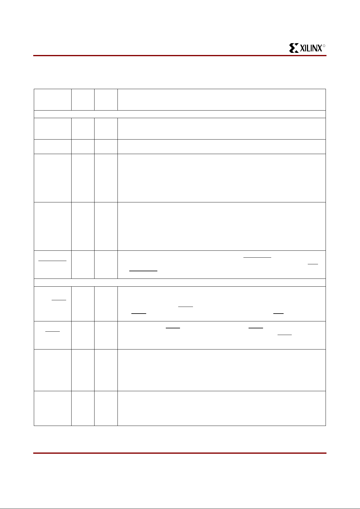
Inside the FPGA, a dedicated Vcc and Ground ring surrounding the logic array provides power to the I/O drivers,
as shown in Figure 21. An independent matrix of Vcc and
Ground lines supplies the interior logic of the device.
This power distribu tion grid provides a stable supply an d
ground for all internal logic, providing the external package
power pins are al l connected and appropriately decoupled.
Typically, a 0.1 µF capacitor connected near the Vcc and
Ground pins of the package will provid e adequate decou pling.
Output buf fers capabl e of driv ing/sinki ng the spe cified 8 mA
loads under specified worst-case conditio ns may be cap able of driving/sinking up to 10 times as much curr ent under
best case conditions.
Noise can be reduced by minimizing external load capacitance and reducing simultaneous output transitions in the
same direction. It may als o be b eneficia l to locate heavily
loaded output buf fers ne ar t he Gro und p ads. The I/O Blo ck
output buffers have a slew-rate limited mode (default)
which should be used where output rise and fall times are
not speed-critical.
Pin Descriptions
There are three types of pins in the XC5200-Series
devices:
• Permanently dedicated pins
• User I/O pins that can have special functions
• Unrestricted user-programmable I/O pins.
Before and duri ng conf igurat ion, al l outpu ts not used for t he
configuration process are 3-stated and pulled high with a
20 kΩ - 100 kΩ pull-up resistor.
After configuration, if an IOB is unused it is configured as
an input with a 20 kΩ - 100 kΩ pull-up resistor.
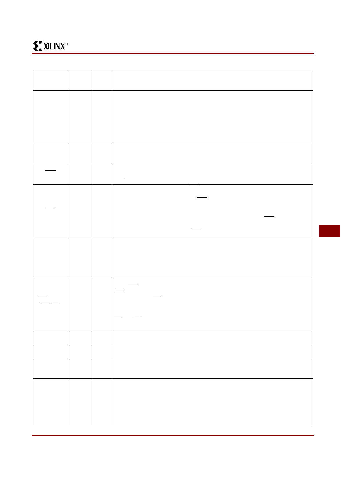
Device pins for XC5200-Series devices are described in
Ta ble 9 . Pin functions during configuration for each of the
seven configuration modes are summarized in “Pin Func-
TDI
TMS
TCK
TDO1
TDO2
TDO
DRCK
IDLE
SEL1
SEL2
RESET
UPDATE
SHIFT
BSCAN
To User
Logic
IBUF
Optional
From
User Logic
To User
Logic
X9000
Figure 20: Boundary Scan Schematic Example
GND
Ground and
Vcc Ring for
I/O Drivers
Vcc
GND
Vcc
Logic
Power Grid
X5422
Figure 21: XC5200-Series Power Distribution
R
XC5200 Series Field Programmable Gate Arrays
7-102 November 5, 1998 (Version 5.2)
tions During Co nf igu ra ti o n” on p age124, in the “Configura -
tion Timing” section.
Table 9: Pin Descriptions
Pin Name
I/O
During
Config.
I/O
After
Config. Pin Description
Permanently Dedicated Pins
VCC I I
Five or more (depe nding on package) co nnecti ons to th e nominal +5 V supply vo ltage.
All must be connected, and each must be decoupled with a 0.01 - 0.1 µF capacitor to
Ground.
GND I I
Four or more (depending on package type) connections to Ground. All mu st be connected.
CCLK I or O I
During confi guration, Con figuration Clock (CCLK) i s an output in Ma ster modes or A synchronous Peri pheral mode, but is an input in Slave mode, Synchronous Peripheral
mode, and Express mode. After configuration, CCLK has a weak pull-up resistor and
can be selected as the Readback Clock. There is no CCLK High time restriction on
XC5200-Series devices, except d uring Readback. See “Violating the Maximum High
and Low Time Specif icatio n for the Read back Clo ck” on pag e 113 for an explanation of
this exception.
DONE I/O O
DONE is a bidire ction al s ignal with an opt ional inter nal pull- up res isto r. As a n out put, i t
indicates th e completion of the c onfiguration process. As an input , a Low level on
DONE can be configured to delay the gl obal logic initialization and the enabling of outputs.
The exact timing, the clock source for the Low-to-High transition, and the optional
pull-up resi stor are s elected as options in the program t hat creat es the co nfigurat ion bit stream. The resistor is included by default.
PROGRAM
II
PROGRAM
is an active Low input that forces the FPGA to clear its configuration mem-
ory. It is us ed to i ni ti at e a co nfi gur at ion c y cle . W he n PR OGRA M
goes High, the FPGA
executes a complete clear cycle, before it goes into a WAIT state and releases INIT
.
The PROGRAM
pin has an optional weak pull-up after configuration.
User I/O Pins That Can Have Special Functions
RDY/BUSY
OI/O
During Peripheral mode configura tion, this pin indicates when it is appropriate to write
another byte o f data into the FPGA. The same status is also available on D7 in Asynchronous Peripheral mode, if a read operation is performed when the device is selected.
After configuration, RDY/BUSY
is a user-programma ble I/O pi n.
RDY/BUSY
is pulled High with a high-impedance pull-up prior to INIT going High.
RCLK
OI/O
During Master Parallel configuration, each change on the A0-A17 outputs is preceded
by a rising edge on RCLK
, a redundant output signal. RCLK is useful for clocked
PROMs. It is rarely used during configuration. After configuration, RCLK
is a user-pro-
grammable I/O pin.
M0, M1, M2 I I/O
As Mode inputs, these pins are sampled before the start of configurati on to determine
the configur ation mode to be used. After configuration, M0, M1, and M2 become user-programmable I/O.
During configu ration, these pins have w eak pull -up resi stors. For the most popul ar configuration m ode, Slave Serial, the mode pin s can thus b e left un connected. A pull-d own
resistor value of 3.3 kΩ is recommended for other modes.
TDO O O
If boundary scan is used, this pi n is the Test Dat a Outpu t. If boundar y scan i s not used,
this pin is a 3-state output, after configuration is completed.
This pin can be user output only when called out by special schematic def initions. To
use this pin, pla ce the libra ry c omponent TDO inst ead of the us ual pa d sy mbol. An out put buffer must still be used.
R
November 5, 1998 (Version 5.2) 7-103
XC5200 Series Field Programmable Gate Arrays
7
TDI, TCK,
TMS
I
I/O
or I
(JTAG)
If boundary scan is used, these pi ns are Test Data In, Test Clock, and Test Mode Select
inputs respe ctively . They com e direct ly from t he pads, bypassing the IOBs . These pi ns
can also be used as inputs to the CLB logic after configuration is completed.
If the BSCAN symbo l is no t pl a ced i n t he de sig n, al l bou nd ar y s can func t i ons ar e i nhib ited once configuration is completed, and these pins become user-p rogrammable I/O.
In this case, t hey must be called ou t by special sche matic definit ions. To use these pi ns,
place the l ibrary com ponents TDI, TCK, and TM S ins tead o f th e us ual pa d sym bols. Input or output buffers must still be used.
HDC O I/O
High During Configuration (HDC) is driven High until the I/O go active. It is available as
a control output indicating that configuration is not yet completed. After configuration,
HDC is a user-programmable I/O pin.
LDC
OI/O
Low During Configuration (LDC
) is driven Low unti l the I/O go activ e. It is avai lable as a
control output indicating that configuration is not yet completed. After configuration,
LDC
is a user-programmable I/O pin.
INIT
I/O I/O
Before and during configuration, INIT
is a bidirectional signal. A 1 kΩ - 10 kΩ external
pull-up resistor is recommended.
As an active-Low open-drain output, INIT
is held Low during the power stabilization and
internal clearing of the configuration memory. As an active-Low input, it can be used
to hold the FPGA in the internal WAIT state before the start of configuration. Master
mode devices stay in a WAIT state an addition al 50 to 250 µs after INIT
has gone High.
During configuration, a Low o n this output indicates that a configuration data error has
occurred. After the I/O go active, INIT
is a user-programmable I/O pin.
GCK1 -
GCK4
Weak
Pull-up
I or I/O
Four Global inputs each drive a dedicated internal global net with short delay and minimal skew. These inter nal global net s can also be drive n from internal logic. If not use d
to drive a global net, any of these pins is a user-programmable I/O pin.
The GCK1-GCK4 pins provide the sh ortest path to the four Global Bu ffers. Any input
pad symbol connected directly to the input of a BUFG symbol is automatically placed on
one of these pins.
CS0
, CS1,
WS
, RS
II/O
These four inputs are used in Asynchronous Peripheral mode. The chip is selected
when CS0
is Low and CS1 is High. While the chip is selected, a Low on Write Strobe
(WS
) loads the data present on the D0 - D7 inputs into the internal data buffer. A Low
on Read Strobe (RS
) changes D7 in to a s ta tus out pu t — Hi gh i f R ead y , L ow i f Bu sy —
and drives D0 - D6 High.
In Express mode, CS1 is used as a serial-enable signal for daisy-chaining.
WS
and RS should be mutu ally excl usive, but if b oth are Low si mult aneously , the Wr ite
Strobe overrides. After configuration, these are user-programma ble I/O pins.
A0 - A17 O I/O
During Master Parallel configuration, these 18 output pins address the configuration
EPROM. After configuration, they are user-programmable I/O pins.
D0 - D7 I I/O
During Master Parallel , Perip heral, a nd Expres s confi guration , thes e eight i nput pins receive configuration data. After configuration, they are user-programmable I/O pins.
DIN I I/O
During Slave Serial or Master Serial configuration, DIN is the serial configuration data
input receiving data on the rising edge of CCLK. Durin g Parallel configuration, DIN is
the D0 input. After configuration, DIN is a user-programmable I/O pin.
DOUT O I/O
During configuration in any mod e but Express mode, DOUT is the serial configuration
data output that can drive the DIN of dais y-chain ed slav e FPGAs. DOUT dat a chan ges
on the falling edge of CCLK.
In Express mode, DOUT is the status output that can drive the CS1 of daisy-chained
FPGAs, to enable and disable downstream devices .
After configuration, DOUT is a user-programmable I/O pi n.
Table 9: Pin Descriptions (Continued)
Pin Name
I/O
During
Config.
I/O
After
Config. Pin Description
R
XC5200 Series Field Programmable Gate Arrays
7-104 November 5, 1998 (Version 5.2)
Configuration
Configurati o n is the process of loading design-speci fic programming data into one or more FPGAs to define the functional operation of the internal blocks and their
interconnections. This is somewhat like loading the command registers of a programmable peripheral chip.
XC5200-Series dev ic es us e s e ve ral hun dr ed b its o f c on fig uration data per CLB and its associated interconnects.
Each configuration bit defines the state of a stat ic memory
cell that controls e ith er a function look-u p t ab le b it, a m u ltiplexer input, or an interconnect pass transistor. The development system translates the design into a netlist file. It
automatically partitions, places and routes the logic and
generates the configuration data in PROM format.
Special Purpose Pins
Three configuration mode pins (M2, M1, M0) are sampled
prior to configuration to determine the configuration mode.
After configuration, these pins can be used as auxiliary I/O
connections. The development system does not use these
resources unless they are explicitly specified in the design
entry. This is done by placing a special pad symbol called
MD2, MD1, or MD0 instead of the i nput or output pad symbol.
In XC5200-Series devices, the mode pins have weak
pull-up resistors during configuration. With all three mode
pins High, Sl ave S e rial m ode is se lec te d, whi ch i s the m os t
popular configuration mode. Therefore, for the most common configuration mode, the mode pins can be left unconnected. (Note, howeve r, that the int ernal pull-up resistor
value can be as high as 100 kΩ.) After configura tio n, th ese
pins can individually have weak pull-up or pull-down resistors, as specified in the design. A pull-down resistor value
of 3.3kΩ is recommended.
These pins are located in the lower left chip corner and are
near the readback nets. This location allows convenient
routing if compatibility with the XC2000 and XC3000 family
conventions of M0/RT, M1/RD is desired.
Configuratio n Modes
XC5200 devices have seven configuration modes. These
modes are sel ected b y a 3 -bit i nput cod e appli ed t o the M2 ,
M1, and M0 inputs . There are three self-loading Mas ter
modes, two Periph er a l mod es, and a Serial Slave mode,
Note :*Peripheral Synchronous can be considered byte-wid e
Slave Parallel
which is use d pri m ari ly f o r d ais y -c ha ined de v i ce s. The seventh mode, called Express mode, is an additional slave
mode that allows high-speed parallel configuration. The
coding for mode selection is shown in Table 10.
Note that the smallest package, VQ64, only supports the
Master Serial, S lave Serial, and Express modes.A detailed
description of each configuration mode, with timing information, is included la ter in t his da ta shee t. Du ring configu ration, some of the I/O pins are used temporarily for the
configuration process. All pins used during configuration
are shown in Table 13 on page 124.
Master Modes
The three Master modes use an internal oscillator to generate a Configur atio n Cl ock ( CCLK) for dri ving pote ntial sl ave
devices. They also generate address and timing for external PROM(s) containing the configuration data.
Master Parallel (Up or Down) modes generate the CCLK
signal and PROM addresses and receive byte parallel
data. The data is internally serialized into the FPGA
data-frame format. The up and down selection generates
starting addresses at either zero or 3FFFF , for compatibility
with different microprocessor addressing conventions. The
Unrestricted User-Programmable I/O Pi ns
I/O
Weak
Pull-up
I/O
These pins ca n be configur ed to be inp ut and/or ou tput after c onfigurati on is comple ted.
Before configuration is completed, these pins have an internal high-value pull-up resistor (20 kΩ - 100 kΩ) that defines the logic level as High.
Table 9: Pin Descriptions (Continued)
Pin Name
I/O
During
Config.
I/O
After
Config. Pin Description
Table 10: Configuration Modes
Mode M2 M1 M0 CCLK Data
Master Serial 0 0 0 output Bit-Serial
Slave Serial 1 1 1 input Bit-Serial
Master
Parallel Up
1 0 0 output Byte-Wide,
increment
from 00000
Master
Parallel Down
1 1 0 output Byte-Wide,
decrement
from 3FFFF
Peripheral
Synchronous*
0 1 1 input Byte-Wide
Peripheral
Asynchronous
1 0 1 output Byte-Wide
Express 0 1 0 input Byte-Wide
Reserved 001 ——
 Loading...