

Page 1

1
XC4000E and XC4000X Series
Table of Contents
14*
XC4000E and XC4000X Series Field Programmable Gate Arrays
XC4000E and XC4000X Series Features. . . . . . . . . . . . . . . . . . . . . . . . . . . . . . . . . . . . . . . . . . . . . . . . 4-5
Low-Voltage Versions Available . . . . . . . . . . . . . . . . . . . . . . . . . . . . . . . . . . . . . . . . . . . . . . . . . . . . . . . 4-5
Additional XC4000X Series Features . . . . . . . . . . . . . . . . . . . . . . . . . . . . . . . . . . . . . . . . . . . . . . . . . . . 4-5
Introduction . . . . . . . . . . . . . . . . . . . . . . . . . . . . . . . . . . . . . . . . . . . . . . . . . . . . . . . . . . . . . . . . . . . . . . . 4-5
Description . . . . . . . . . . . . . . . . . . . . . . . . . . . . . . . . . . . . . . . . . . . . . . . . . . . . . . . . . . . . . . . . . 4-6
Taking Advantage of Reconfiguration. . . . . . . . . . . . . . . . . . . . . . . . . . . . . . . . . . . . . . . . . . . . . 4-6
XC4000E and XC4000X Series Compared to the XC4000 . . . . . . . . . . . . . . . . . . . . . . . . . . . . . . . . . . 4-7
Improvements in XC4000E and XC4000X . . . . . . . . . . . . . . . . . . . . . . . . . . . . . . . . . . . . . . . . . 4-7
Additional Improvements in XC4000X Only . . . . . . . . . . . . . . . . . . . . . . . . . . . . . . . . . . . . . . . . 4-8
Detailed Functional Description . . . . . . . . . . . . . . . . . . . . . . . . . . . . . . . . . . . . . . . . . . . . . . . . . . . . . . . 4-9
Basic Building Blocks . . . . . . . . . . . . . . . . . . . . . . . . . . . . . . . . . . . . . . . . . . . . . . . . . . . . . . . . . 4-9
Configurable Logic Blocks (CLBs) . . . . . . . . . . . . . . . . . . . . . . . . . . . . . . . . . . . . . . . . . . . . . . . 4-9
Function Generators. . . . . . . . . . . . . . . . . . . . . . . . . . . . . . . . . . . . . . . . . . . . . . . . . . . . . . 4-9
Flip-Flops . . . . . . . . . . . . . . . . . . . . . . . . . . . . . . . . . . . . . . . . . . . . . . . . . . . . . . . . . . . . . . 4-10
Latches (XC4000X only). . . . . . . . . . . . . . . . . . . . . . . . . . . . . . . . . . . . . . . . . . . . . . . . . . . 4-10
Clock Input . . . . . . . . . . . . . . . . . . . . . . . . . . . . . . . . . . . . . . . . . . . . . . . . . . . . . . . . . . . . . 4-10
Clock Enable. . . . . . . . . . . . . . . . . . . . . . . . . . . . . . . . . . . . . . . . . . . . . . . . . . . . . . . . . . . . 4-10
Set/Reset . . . . . . . . . . . . . . . . . . . . . . . . . . . . . . . . . . . . . . . . . . . . . . . . . . . . . . . . . . . . . . 4-11
Global Set/Reset. . . . . . . . . . . . . . . . . . . . . . . . . . . . . . . . . . . . . . . . . . . . . . . . . . . . . . . . . 4-11
Data Inputs and Outputs. . . . . . . . . . . . . . . . . . . . . . . . . . . . . . . . . . . . . . . . . . . . . . . . . . . 4-11
Control Signals . . . . . . . . . . . . . . . . . . . . . . . . . . . . . . . . . . . . . . . . . . . . . . . . . . . . . . . . . . 4-11
Using FPGA Flip-Flops and Latches. . . . . . . . . . . . . . . . . . . . . . . . . . . . . . . . . . . . . . . . . . 4-11
Using Function Generators as RAM. . . . . . . . . . . . . . . . . . . . . . . . . . . . . . . . . . . . . . . . . . 4-11
Fast Carry Logic . . . . . . . . . . . . . . . . . . . . . . . . . . . . . . . . . . . . . . . . . . . . . . . . . . . . . . . . . 4-18
Input/Output Blocks (IOBs). . . . . . . . . . . . . . . . . . . . . . . . . . . . . . . . . . . . . . . . . . . . . . . . . . . . . 4-21
IOB Input Signals . . . . . . . . . . . . . . . . . . . . . . . . . . . . . . . . . . . . . . . . . . . . . . . . . . . . . . . . 4-21
IOB Output Signals. . . . . . . . . . . . . . . . . . . . . . . . . . . . . . . . . . . . . . . . . . . . . . . . . . . . . . . 4-24
Other IOB Options . . . . . . . . . . . . . . . . . . . . . . . . . . . . . . . . . . . . . . . . . . . . . . . . . . . . . . . 4-26
Three-State Buffers. . . . . . . . . . . . . . . . . . . . . . . . . . . . . . . . . . . . . . . . . . . . . . . . . . . . . . . . . . . 4-27
Three-State Buffer Modes. . . . . . . . . . . . . . . . . . . . . . . . . . . . . . . . . . . . . . . . . . . . . . . . . . 4-27
Three-State Buffer Examples . . . . . . . . . . . . . . . . . . . . . . . . . . . . . . . . . . . . . . . . . . . . . . . 4-27
Wide Edge Decoders . . . . . . . . . . . . . . . . . . . . . . . . . . . . . . . . . . . . . . . . . . . . . . . . . . . . . . . . . 4-28
On-Chip Oscillator. . . . . . . . . . . . . . . . . . . . . . . . . . . . . . . . . . . . . . . . . . . . . . . . . . . . . . . . . . . . 4-28
Programmable Interconnect . . . . . . . . . . . . . . . . . . . . . . . . . . . . . . . . . . . . . . . . . . . . . . . . . . . . . . . . . . 4-29
Interconnect Overview . . . . . . . . . . . . . . . . . . . . . . . . . . . . . . . . . . . . . . . . . . . . . . . . . . . . . . . . 4-29
CLB Routing Connections. . . . . . . . . . . . . . . . . . . . . . . . . . . . . . . . . . . . . . . . . . . . . . . . . . . . . . 4-29
Programmable Switch Matrices . . . . . . . . . . . . . . . . . . . . . . . . . . . . . . . . . . . . . . . . . . . . . 4-30
Single-Length Lines . . . . . . . . . . . . . . . . . . . . . . . . . . . . . . . . . . . . . . . . . . . . . . . . . . . . . . 4-30
Double-Length Lines. . . . . . . . . . . . . . . . . . . . . . . . . . . . . . . . . . . . . . . . . . . . . . . . . . . . . . 4-32
Quad Lines (XC4000X only). . . . . . . . . . . . . . . . . . . . . . . . . . . . . . . . . . . . . . . . . . . . . . . . 4-32
Longlines. . . . . . . . . . . . . . . . . . . . . . . . . . . . . . . . . . . . . . . . . . . . . . . . . . . . . . . . . . . . . . . 4-32
Direct Interconnect (XC4000X only) . . . . . . . . . . . . . . . . . . . . . . . . . . . . . . . . . . . . . . . . . . 4-33
I/O Routing . . . . . . . . . . . . . . . . . . . . . . . . . . . . . . . . . . . . . . . . . . . . . . . . . . . . . . . . . . . . . . . . . 4-33
Octal I/O Routing (XC4000X only) . . . . . . . . . . . . . . . . . . . . . . . . . . . . . . . . . . . . . . . . . . . 4-33
Global Nets and Buffers . . . . . . . . . . . . . . . . . . . . . . . . . . . . . . . . . . . . . . . . . . . . . . . . . . . . . . . 4-36
Global Nets and Buffers (XC4000E only) . . . . . . . . . . . . . . . . . . . . . . . . . . . . . . . . . . . . . . 4-36
Global Nets and Buffers (XC4000X only) . . . . . . . . . . . . . . . . . . . . . . . . . . . . . . . . . . . . . . 4-38
Power Distribution. . . . . . . . . . . . . . . . . . . . . . . . . . . . . . . . . . . . . . . . . . . . . . . . . . . . . . . . . . . . . . . . . . 4-40
4-1
Page 2

XC4000E and XC4000X Series Table of Contents
Pin Descriptions . . . . . . . . . . . . . . . . . . . . . . . . . . . . . . . . . . . . . . . . . . . . . . . . . . . . . . . . . . . . . . . . . . . 4-40
Boundary Scan . . . . . . . . . . . . . . . . . . . . . . . . . . . . . . . . . . . . . . . . . . . . . . . . . . . . . . . . . . . . . . . . . . . . 4-43
Data Registers . . . . . . . . . . . . . . . . . . . . . . . . . . . . . . . . . . . . . . . . . . . . . . . . . . . . . . . . . . . . . . 4-43
Instruction Set. . . . . . . . . . . . . . . . . . . . . . . . . . . . . . . . . . . . . . . . . . . . . . . . . . . . . . . . . . . . . . . 4-45
Bit Sequence. . . . . . . . . . . . . . . . . . . . . . . . . . . . . . . . . . . . . . . . . . . . . . . . . . . . . . . . . . . . . . . . 4-45
Including Boundary Scan in a Schematic . . . . . . . . . . . . . . . . . . . . . . . . . . . . . . . . . . . . . . . . . . 4-45
Avoiding Inadvertent Boundary Scan . . . . . . . . . . . . . . . . . . . . . . . . . . . . . . . . . . . . . . . . . . . . . 4-46
Configuration. . . . . . . . . . . . . . . . . . . . . . . . . . . . . . . . . . . . . . . . . . . . . . . . . . . . . . . . . . . . . . . . . . . . . . 4-46
Special Purpose Pins . . . . . . . . . . . . . . . . . . . . . . . . . . . . . . . . . . . . . . . . . . . . . . . . . . . . . . . . . 4-46
Configuration Modes. . . . . . . . . . . . . . . . . . . . . . . . . . . . . . . . . . . . . . . . . . . . . . . . . . . . . . . . . . 4-47
Master Modes. . . . . . . . . . . . . . . . . . . . . . . . . . . . . . . . . . . . . . . . . . . . . . . . . . . . . . . . . . . 4-47
Additional Address lines in XC4000 devices. . . . . . . . . . . . . . . . . . . . . . . . . . . . . . . . . . . . 4-47
Peripheral Modes . . . . . . . . . . . . . . . . . . . . . . . . . . . . . . . . . . . . . . . . . . . . . . . . . . . . . . . . 4-47
Slave Serial Mode. . . . . . . . . . . . . . . . . . . . . . . . . . . . . . . . . . . . . . . . . . . . . . . . . . . . . . . . 4-47
Setting CCLK Frequency . . . . . . . . . . . . . . . . . . . . . . . . . . . . . . . . . . . . . . . . . . . . . . . . . . . . . . 4-49
Data Stream Format . . . . . . . . . . . . . . . . . . . . . . . . . . . . . . . . . . . . . . . . . . . . . . . . . . . . . . . . . . 4-49
Cyclic Redundancy Check (CRC) for Configuration and Readback. . . . . . . . . . . . . . . . . . . . . . 4-50
Configuration Sequence . . . . . . . . . . . . . . . . . . . . . . . . . . . . . . . . . . . . . . . . . . . . . . . . . . . . . . . 4-51
Configuration Memory Clear. . . . . . . . . . . . . . . . . . . . . . . . . . . . . . . . . . . . . . . . . . . . . . . . 4-51
Initialization. . . . . . . . . . . . . . . . . . . . . . . . . . . . . . . . . . . . . . . . . . . . . . . . . . . . . . . . . . . . . 4-52
Delaying Configuration After Power-Up . . . . . . . . . . . . . . . . . . . . . . . . . . . . . . . . . . . . . . . 4-52
Start-Up. . . . . . . . . . . . . . . . . . . . . . . . . . . . . . . . . . . . . . . . . . . . . . . . . . . . . . . . . . . . . . . . 4-52
DONE Goes High to Signal End of Configuration. . . . . . . . . . . . . . . . . . . . . . . . . . . . . . . . 4-55
Release of User I/O After DONE Goes High . . . . . . . . . . . . . . . . . . . . . . . . . . . . . . . . . . . 4-55
Release of Global Set/Reset After DONE Goes High. . . . . . . . . . . . . . . . . . . . . . . . . . . . . 4-55
Configuration Complete After DONE Goes High . . . . . . . . . . . . . . . . . . . . . . . . . . . . . . . . 4-55
Configuration Through the Boundary Scan Pins. . . . . . . . . . . . . . . . . . . . . . . . . . . . . . . . . . . . . 4-55
Readback . . . . . . . . . . . . . . . . . . . . . . . . . . . . . . . . . . . . . . . . . . . . . . . . . . . . . . . . . . . . . . . . . . . . . . . . 4-56
Readback Options . . . . . . . . . . . . . . . . . . . . . . . . . . . . . . . . . . . . . . . . . . . . . . . . . . . . . . . . . . . 4-57
Read Capture . . . . . . . . . . . . . . . . . . . . . . . . . . . . . . . . . . . . . . . . . . . . . . . . . . . . . . . . . . . 4-57
Read Abort . . . . . . . . . . . . . . . . . . . . . . . . . . . . . . . . . . . . . . . . . . . . . . . . . . . . . . . . . . . . . 4-57
Clock Select . . . . . . . . . . . . . . . . . . . . . . . . . . . . . . . . . . . . . . . . . . . . . . . . . . . . . . . . . . . . 4-57
Violating the Maximum High and Low Time Specification for the Readback Clock . . . . . . . . . . 4-57
Readback with the XChecker Cable. . . . . . . . . . . . . . . . . . . . . . . . . . . . . . . . . . . . . . . . . . . . . . 4-57
XC4000E/EX/XL Program Readback Switching Characteristic Guidelines . . . . . . . . . . . . . . . . 4-58
Configuration Timing. . . . . . . . . . . . . . . . . . . . . . . . . . . . . . . . . . . . . . . . . . . . . . . . . . . . . . . . . . . . . . . . 4-61
Slave Serial Mode. . . . . . . . . . . . . . . . . . . . . . . . . . . . . . . . . . . . . . . . . . . . . . . . . . . . . . . . . . . . 4-61
Master Serial Mode. . . . . . . . . . . . . . . . . . . . . . . . . . . . . . . . . . . . . . . . . . . . . . . . . . . . . . . . . . . 4-62
Master Parallel Modes . . . . . . . . . . . . . . . . . . . . . . . . . . . . . . . . . . . . . . . . . . . . . . . . . . . . . . . . 4-63
Additional Address lines in XC4000 devices. . . . . . . . . . . . . . . . . . . . . . . . . . . . . . . . . . . . 4-63
Synchronous Peripheral Mode . . . . . . . . . . . . . . . . . . . . . . . . . . . . . . . . . . . . . . . . . . . . . . . . . . 4-65
Asynchronous Peripheral Mode . . . . . . . . . . . . . . . . . . . . . . . . . . . . . . . . . . . . . . . . . . . . . . . . . 4-67
Write to FPGA. . . . . . . . . . . . . . . . . . . . . . . . . . . . . . . . . . . . . . . . . . . . . . . . . . . . . . . . . . . 4-67
Status Read . . . . . . . . . . . . . . . . . . . . . . . . . . . . . . . . . . . . . . . . . . . . . . . . . . . . . . . . . . . . 4-67
Configuration Switching Characteristics . . . . . . . . . . . . . . . . . . . . . . . . . . . . . . . . . . . . . . . . . . . . . . . . . 4-69
Master Modes (XC4000E/EX). . . . . . . . . . . . . . . . . . . . . . . . . . . . . . . . . . . . . . . . . . . . . . . . . . . 4-69
Master Modes (XC4000XL) . . . . . . . . . . . . . . . . . . . . . . . . . . . . . . . . . . . . . . . . . . . . . . . . . . . . 4-69
Slave and Peripheral Modes(All) . . . . . . . . . . . . . . . . . . . . . . . . . . . . . . . . . . . . . . . . . . . . . . . . 4-69
XC4000XL Switching Characteristics . . . . . . . . . . . . . . . . . . . . . . . . . . . . . . . . . . . . . . . . . . . . . . . . . . . 4-70
Definition of Terms . . . . . . . . . . . . . . . . . . . . . . . . . . . . . . . . . . . . . . . . . . . . . . . . . . . . . . . . . . . 4-70
Additional Specifications. . . . . . . . . . . . . . . . . . . . . . . . . . . . . . . . . . . . . . . . . . . . . . . . . . . . . . . 4-70
Absolute Maximum Ratings . . . . . . . . . . . . . . . . . . . . . . . . . . . . . . . . . . . . . . . . . . . . . . . . . . . . 4-70
Recommended Operating Conditions. . . . . . . . . . . . . . . . . . . . . . . . . . . . . . . . . . . . . . . . . . . . . 4-70
DC Characteristics Over Recommended Operating Conditions. . . . . . . . . . . . . . . . . . . . . . . . . 4-71
XC4000XL Global Buffer Switching Characteristic Guidelines . . . . . . . . . . . . . . . . . . . . . . . . . . 4-72
XC4000XL CLB Switching Characteristic Guidelines . . . . . . . . . . . . . . . . . . . . . . . . . . . . . . . . . 4-73
4-2
Page 3

XC4000XL CLB RAM Synchronous (Edge-Triggered) Write Timing . . . . . . . . . . . . . . . . . . . . . 4-76
XC4000XL CLB Dual-Port RAM Synchronous (Edge-Triggered) Write Timing . . . . . . . . . . . . . 4-76
XC4000XL Pin-to-Pin Output Parameter Guidelines . . . . . . . . . . . . . . . . . . . . . . . . . . . . . . . . . . . . . . . 4-77
Capacitive Load Factor. . . . . . . . . . . . . . . . . . . . . . . . . . . . . . . . . . . . . . . . . . . . . . . . . . . . . . . . 4-78
XC4000XL Pin-to-Pin Input Parameter Guidelines. . . . . . . . . . . . . . . . . . . . . . . . . . . . . . . . . . . . . . . . . 4-79
XC4000XL Global Low Skew Clock, Set-Up and Hold . . . . . . . . . . . . . . . . . . . . . . . . . . . . . . . . 4-79
XC4000XL BUFGE #s 3, 4, 7, & 8 Global Early Clock, Set-up and Hold for IFF and FCL. . . . . 4-80
XC4000XL BUFGE #s 1, 2, 5, & 6 Global Early Clock, Set-up and Hold for IFF and FCL. . . . . 4-81
XC4000XL . . . . . . . . . . . . . . . . . . . . . . . . . . . . . . . . . . . . . . . . . . . . . . . . . . . . . . . . . . . . . . . . . IOB Input
Switching Characteristic Guidelines . . . . . . . . . . . . . . . . . . . . . . . . . . . . . . . . . . . . . . . . . . . . . . 4-82
XC4000XL IOB Output Switching Characteristic Guidelines . . . . . . . . . . . . . . . . . . . . . . . . . . . 4-83
XC4000EX Switching Characteristics. . . . . . . . . . . . . . . . . . . . . . . . . . . . . . . . . . . . . . . . . . . . . . . . . . . 4-84
Definition of Terms . . . . . . . . . . . . . . . . . . . . . . . . . . . . . . . . . . . . . . . . . . . . . . . . . . . . . . . . . . . 4-84
XC4000EX Absolute Maximum Ratings . . . . . . . . . . . . . . . . . . . . . . . . . . . . . . . . . . . . . . . . . . . 4-84
XC4000EX Recommended Operating Conditions . . . . . . . . . . . . . . . . . . . . . . . . . . . . . . . . . . . 4-84
XC4000EX DC Characteristics Over Recommended Operating Conditions . . . . . . . . . . . . . . . 4-85
XC4000EX Longline and Wide Decoder Timing Guidelines. . . . . . . . . . . . . . . . . . . . . . . . . . . . . . . . . . 4-86
XC4000EX Wide Decoder Switching Characteristic Guidelines. . . . . . . . . . . . . . . . . . . . . . . . . 4-86
XC4000EX CLB Switching Characteristic Guidelines. . . . . . . . . . . . . . . . . . . . . . . . . . . . . . . . . 4-87
XC4000EX CLB RAM Synchronous (Edge-Triggered) Write Timing . . . . . . . . . . . . . . . . . . . . . 4-89
XC4000EX CLB Dual-Port RAM Synchronous (Edge-Triggered) Write Timing . . . . . . . . . . . . . 4-89
XC4000EX CLB RAM Asynchronous (Level-Sensitive) Write and Read Operation Guidelines. 4-90
XC4000EX CLB RAM Asynchronous (Level-Sensitive) Timing Characteristics. . . . . . . . . . . . . 4-91
XC4000EX Pin-to-Pin Output Parameter Guidelines . . . . . . . . . . . . . . . . . . . . . . . . . . . . . . . . . . . . . . . 4-92
XC4000EX Output MUX, Clock to Out . . . . . . . . . . . . . . . . . . . . . . . . . . . . . . . . . . . . . . . . . . . . 4-92
XC4000EX Output Level and Slew Rate Adjustments . . . . . . . . . . . . . . . . . . . . . . . . . . . . . . . . 4-92
XC4000EX Pin-to-Pin Input Parameter Guidelines. . . . . . . . . . . . . . . . . . . . . . . . . . . . . . . . . . . . . . . . . 4-93
XC4000EX Global Early Clock, Set-Up and Hold for IFF . . . . . . . . . . . . . . . . . . . . . . . . . . . . . . 4-93
XC4000EX Global Early Clock, Set-Up and Hold for FCL . . . . . . . . . . . . . . . . . . . . . . . . . . . . . 4-93
XC4000EX Input Threshold Adjustments . . . . . . . . . . . . . . . . . . . . . . . . . . . . . . . . . . . . . . . . . . 4-93
XC4000EX IOB Input Switching Characteristic Guidelines. . . . . . . . . . . . . . . . . . . . . . . . . . . . . 4-94
XC4000EX IOB Input Switching Characteristic Guidelines (Continued). . . . . . . . . . . . . . . . . . . 4-95
XC4000EX IOB Output Switching Characteristic Guidelines . . . . . . . . . . . . . . . . . . . . . . . . . . . 4-96
XC4000E Switching Characteristics . . . . . . . . . . . . . . . . . . . . . . . . . . . . . . . . . . . . . . . . . . . . . . . . . . . . 4-97
Definition of Terms . . . . . . . . . . . . . . . . . . . . . . . . . . . . . . . . . . . . . . . . . . . . . . . . . . . . . . . . . . . 4-97
XC4000E Absolute Maximum Ratings . . . . . . . . . . . . . . . . . . . . . . . . . . . . . . . . . . . . . . . . . . . . 4-97
XC4000E Recommended Operating Conditions . . . . . . . . . . . . . . . . . . . . . . . . . . . . . . . . . . . . 4-97
XC4000E DC Characteristics Over Operating Conditions . . . . . . . . . . . . . . . . . . . . . . . . . . . . . 4-98
XC4000E Global Buffer Switching Characteristic Guidelines . . . . . . . . . . . . . . . . . . . . . . . . . . . 4-98
XC4000E Horizontal Longline Switching Characteristic Guidelines . . . . . . . . . . . . . . . . . . . . . . 4-99
XC4000E Wide Decoder Switching Characteristic Guidelines . . . . . . . . . . . . . . . . . . . . . . . . . . 4-100
XC4000E CLB Switching Characteristic Guidelines . . . . . . . . . . . . . . . . . . . . . . . . . . . . . . . . . . 4-101
XC4000E CLB RAM Synchronous (Edge-Triggered) Write Timing . . . . . . . . . . . . . . . . . . . . . . 4-104
XC4000E CLB Dual-Port RAM Synchronous (Edge-Triggered) Write Timing . . . . . . . . . . . . . . 4-104
XC4000E CLB Level-Sensitive RAM Switching Characteristic Guidelines. . . . . . . . . . . . . . . . . 4-105
XC4000E CLB Level-Sensitive RAM Timing Characteristics . . . . . . . . . . . . . . . . . . . . . . . . . . . 4-106
XC4000E Guaranteed Input and Output Parameters (Pin-to-Pin, TTL I/O) . . . . . . . . . . . . . . . . 4-107
XC4000E IOB Input Switching Characteristic Guidelines. . . . . . . . . . . . . . . . . . . . . . . . . . . . . . 4-108
XC4000E IOB Output Switching Characteristic Guidelines . . . . . . . . . . . . . . . . . . . . . . . . . . . . 4-110
XC4000E Boundary Scan (JTAG) Switching Characteristic Guidelines. . . . . . . . . . . . . . . . . . . 4-112
Device-Specific Pinout Tables . . . . . . . . . . . . . . . . . . . . . . . . . . . . . . . . . . . . . . . . . . . . . . . . . . . . . . . . 4-113
Pin Locations for XC4003E Devices. . . . . . . . . . . . . . . . . . . . . . . . . . . . . . . . . . . . . . . . . . . . . . 4-113
Pin Locations for XC4005E/XL Devices . . . . . . . . . . . . . . . . . . . . . . . . . . . . . . . . . . . . . . . . . . . 4-114
Pin Locations for XC4006E Devices. . . . . . . . . . . . . . . . . . . . . . . . . . . . . . . . . . . . . . . . . . . . . . 4-115
Pin Locations for XC4008E Devices. . . . . . . . . . . . . . . . . . . . . . . . . . . . . . . . . . . . . . . . . . . . . . 4-117
Pin Locations for XC4010E/XL Devices . . . . . . . . . . . . . . . . . . . . . . . . . . . . . . . . . . . . . . . . . . . 4-118
4-3
Page 4

XC4000E and XC4000X Series Table of Contents
Pin Locations for XC4013E/XL Devices . . . . . . . . . . . . . . . . . . . . . . . . . . . . . . . . . . . . . . . . . . . 4-120
Pin Locations for XC4020E/XL Devices . . . . . . . . . . . . . . . . . . . . . . . . . . . . . . . . . . . . . . . . . . . 4-123
Pin Locations for XC4025E, XC4028EX/XL Devices . . . . . . . . . . . . . . . . . . . . . . . . . . . . . . . . . 4-125
Pin Locations for XC4036EX/XL. . . . . . . . . . . . . . . . . . . . . . . . . . . . . . . . . . . . . . . . . . . . . . . . . 4-128
Pin Locations for XC4044XL Devices. . . . . . . . . . . . . . . . . . . . . . . . . . . . . . . . . . . . . . . . . . . . . 4-131
Pin Locations for XC4052XL Devices. . . . . . . . . . . . . . . . . . . . . . . . . . . . . . . . . . . . . . . . . . . . . 4-135
Pin Locations for XC4062XL Devices. . . . . . . . . . . . . . . . . . . . . . . . . . . . . . . . . . . . . . . . . . . . . 4-139
Pin Locations for XC4085XL Devices. . . . . . . . . . . . . . . . . . . . . . . . . . . . . . . . . . . . . . . . . . . . . . . . . . . 4-143
Product Availability . . . . . . . . . . . . . . . . . . . . . . . . . . . . . . . . . . . . . . . . . . . . . . . . . . . . . . . . . . . . . . . . . 4-151
User I/O Per Package. . . . . . . . . . . . . . . . . . . . . . . . . . . . . . . . . . . . . . . . . . . . . . . . . . . . . . . . . . . . . . . 4-153
Ordering Information. . . . . . . . . . . . . . . . . . . . . . . . . . . . . . . . . . . . . . . . . . . . . . . . . . . . . . . . . . . . . . . . 4-154
4-4
Page 5

book
1
March 30, 1998 (Version 1.5)
14*
XC4000E and XC4000X Series
Features
Note: XC4000 Series devices described in this data sheet
include the XC4000E family and XC4000X Series.
XC4000X Series devices described in this data sheet
include the XC4000EX and XC4000XL families. Separate
data sheets are available for two other Families in the
XC4000X series, the XC4000XLT and XC4000XV. This
information does not apply to the older Xilinx families:
XC4000, XC4000A, XC4000D, XC4000H, or XC4000L. F or
information on these devices, see the Xilinx WEBLINX at
http://www.xilinx.com.
• System featured Field-Programmable Gate Arrays
- Select-RAMTM memory: on-chip ultra-fast RAM with
- synchronous write option
- dual-port RAM option
- Fully PCI compliant (speed grades -2 and faster)
- Abundant flip-flops
- Flexible function generators
- Dedicated high-speed carry logic
- Wide edge decoders on each edge
- Hierarchy of interconnect lines
- Internal 3-state bus capability
- 8 global low-skew clock or signal distribution
networks
• System Performance beyond 80 MHz
• Flexible Array Architecture
• Low Power Segmented Routing Architecture
• Systems-Oriented Features
- IEEE 1149.1-compatible boundary scan logic
support
- Individually programmable output slew rate
- Programmable input pull-up or pull-down resistors
- 12-mA sink current per XC4000E output
• Configured by Loading Binary File
- Unlimited reprogrammability
• Readback Capability
- Program verification
- Internal node observability
• Backward Compatible with XC4000 Devices
• Development System runs on most common computer
platforms
- Interfaces to popular design environments
- Fully automatic mapping, placement and routing
- Interactive design editor for design optimization
XC4000E and XC4000X Series
Field Programmable Gate Arrays
Product Specification
Low-Voltage Versions Available
• Low-Voltage Devices Function at 3.0 - 3.6 Volts
• XC4000XL: High Performance Low-Voltage Versions of
XC4000EX devices
Additional XC4000X Series Features
• Highest Performance — 3.3 V XC4000XL
• Highest Capacity — Over 180,000 Usable Gates
• 5V tolerant I/Os on XC4000XL
• 0.35µ SRAM process for XC4000XL
• Additional Routing Over XC4000E
- almost twice the routing capacity for high-density
designs
• Buffered Interconnect for Maximum Speed
• New Latch Capability in Configurable Logic Blocks
• Improved VersaRing
Pinout Flexibility
• 12-mA Sink Current Per XC4000X Output
• Flexible New High-Speed Clock Network
- 8 additional Early Buffers for shorter clock delays
- Virtually unlimited number of clock signals
• Optional Multiplexer or 2-input Function Generator on
Device Outputs
• 4 Additional Address Bits in Master Parallel
Configuration Mode
• XC4000XLT devices, optimized for PCI applications,
are available.
• The XC4000XV Family offers the highest density with
0.25 micron 2.5 volt technology.
TM
I/O Interconnect for Better Fixed
Introduction
XC4000 Series high-performance, high-capacity Field Programmable Gate Arrays (FPGAs) provide the benefits of
custom CMOS VLSI, while avoiding the initial cost, long
development cycle, and inherent risk of a conventional
masked gate array.
The result of thirteen years of FPGA design experience and
feedback from thousands of customers, these FPGAs combine architectural versatility, on-chip Select-RAM memory
with edge-triggered and dual-port modes, increased speed,
abundant routing resources, and new, sophisticated software to achieve fully automated implementation of complex, high-density, high-performance designs.
The XC4000E and XC4000X Series currently have 20
members, as shown in Table 2.
March 30, 1998 (Version 1.5) 4-5
Page 6

XC4000E and XC4000X Series Field Programmable Gate Arrays
Note:
All functionality in low-voltage families is the same as
in the corresponding 5-Volt family, except where numerical
references are made to timing or power.
Table 2: XC4000E and XC4000X Series Field Programmable Gate Arrays
Max Logic
Logic
Device
XC4002XL 152 1,600 2,048 1,000 - 3,000 8 x 8 64 256 64
XC4003E 238 3,000 3,200 2,000 - 5,000 10 x 10 100 360 80
XC4005E/XL 466 5,000 6,272 3,000 - 9,000 14 x 14 196 616 112
XC4006E 608 6,000 8,192 4,000 - 12,000 16 x 16 256 768 128
XC4008E 770 8,000 10,368 6,000 - 15,000 18 x 18 324 936 144
XC4010E/XL 950 10,000 12,800 7,000 - 20,000 20 x 20 400 1,120 160
XC4013E/XL 1368 13,000 18,432 10,000 - 30,000 24 x 24 576 1,536 192
XC4020E/XL 1862 20,000 25,088 13,000 - 40,000 28 x 28 784 2,016 224
XC4025E 2432 25,000 32,768 15,000 - 45,000 32 x 32 1,024 2,560 256
XC4028EX/XL 2432 28,000 32,768 18,000 - 50,000 32 x 32 1,024 2,560 256
XC4036EX/XL 3078 36,000 41,472 22,000 - 65,000 36 x 36 1,296 3,168 288
XC4044XL 3800 44,000 51,200 27,000 - 80,000 40 x 40 1,600 3,840 320
XC4052XL 4598 52,000 61,952 33,000 - 100,000 44 x 44 1,936 4,576 352
XC4062XL 5472 62,000 73,728 40,000 - 130,000 48 x 48 2,304 5,376 384
XC4085XL 7448 85,000 100,352 55,000 - 180,000 56 x 56 3,136 7,168 448
* Max values of Typical Gate Range include 20-30% of CLBs used as RAM.
Cells
Gates
(No RAM)
Max. RAM
Bits
(No Logic)
Typical
Gate Range
(Logic and RAM)*
CLB
Matrix
Total
CLBs
Number
of
Flip-Flops
Max.
User I/O
Description
XC4000 Series devices are implemented with a regular,
flexible, programmable architecture of Configurable Logic
Blocks (CLBs), interconnected by a powerful hierarchy of
versatile routing resources, and surrounded by a perimeter
of programmable Input/Output Blocks (IOBs). They have
generous routing resources to accommodate the most
complex interconnect patterns.
The devices are customized by loading configuration data
into internal memory cells. The FPGA can either actively
read its configuration data from an external serial or byteparallel PROM (master modes), or the configuration data
can be written into the FPGA from an external device (slave
and peripheral modes).
XC4000 Series FPGAs are supported by powerful and
sophisticated software, covering every aspect of design
from schematic or behavioral entry, floorplanning, simulation, automatic block placement and routing of interconnects, to the creation, downloading, and readback of the
configuration bit stream.
Because Xilinx FPGAs can be reprogrammed an unlimited
number of times, they can be used in innovative designs
where hardware is changed dynamically, or where hardware must be adapted to different user applications.
FPGAs are ideal for shortening design and development
cycles, and also offer a cost-effective solution for production rates well beyond 5,000 systems per month. F or lowest
high-volume unit cost, a design can first be implemented in
the XC4000E or XC4000X, then migrated to one of Xilinx’
compatible HardWire mask-programmed devices.
Taking Advantage of Reconfiguration
FPGA devices can be reconfigured to change logic function
while resident in the system. This capability gives the system designer a new degree of freedom not available with
any other type of logic.
Hardware can be changed as easily as software. Design
updates or modifications are easy, and can be made to
products already in the field. An FPGA can even be reconfigured dynamically to perform different functions at different times.
Reconfigurable logic can be used to implement system
self-diagnostics, create systems capable of being reconfigured for different environments or oper ations , or implement
multi-purpose hardware for a given application. As an
added benefit, using reconfigurable FPGA devices simplifies hardware design and debugging and shortens product
time-to-market.
4-6 March 30, 1998 (Version 1.5)
Page 7

XC4000E and XC4000X Series
Compared to the XC4000
For readers already familiar with the XC4000 family of Xilinx Field Programmable Gate Arrays, the major new features in the XC4000 Series devices are listed in this
section. The biggest advantages of XC4000E and
XC4000X devices are significantly increased system
speed, greater capacity, and new architectural features,
particularly Select-RAM memor y. The XC4000X devices
also offer many new routing features, including special
high-speed clock buffers that can be used to capture input
data with minimal delay.
Any XC4000E device is pinout- and bitstream-compatible
with the corresponding XC4000 device. An existing
XC4000 bitstream can be used to program an XC4000E
device. However, since the XC4000E includes many new
features, an XC4000E bitstream cannot be loaded into an
XC4000 device.
XC4000X Series devices are not bitstream-compatible with
equivalent array size devices in the XC4000 or XC4000E
families. However, equivalent array size devices, such as
the XC4025, XC4025E, XC4028EX, and XC4028XL, are
pinout-compatible.
Improvements in XC4000E and XC4000X
Increased System Speed
XC4000E and XC4000X devices can run at synchronous
system clock rates of up to 80 MHz, and internal performance can exceed 150 MHz. This increase in performance
over the previous families stems from improvements in
both device processing and system architecture. XC4000
Series devices use a sub-micron multi-layer metal process .
In addition, many architectural improvements have been
made, as described below.
The XC4000XL family is a high performance 3.3V family
based on 0.35µ SRAM technology and supports system
speeds to 80 MHz.
PCI Compliance
XC4000 Series -2 and faster speed grades are fully PCI
compliant. XC4000E and XC4000X devices can be used to
implement a one-chip PCI solution.
Carry Logic
The speed of the carry logic chain has increased dramatically. Some parameters, such as the delay on the carry
chain through a single CLB (TBYP), have improved by as
much as 50% from XC4000 values. See “Fast Carry Logic”
on page 4-18 for more information.
Select-RAM Memory: Edge-Triggered, Synchronous
RAM Modes
The RAM in any CLB can be configured for synchronous,
edge-triggered, write operation. The read operation is not
affected by this change to an edge-triggered write.
Dual-Port RAM
A separate option converts the 16x2 RAM in any CLB into a
16x1 dual-port RAM with simultaneous Read/Write.
The function generators in each CLB can be configured as
either level-sensitive (asynchronous) single-port RAM,
edge-triggered (synchronous) single-port RAM, edge-triggered (synchronous) dual-port RAM, or as combinatorial
logic.
Configurable RAM Content
The RAM content can now be loaded at configuration time,
so that the RAM starts up with user-defined data.
H Function Generator
In current XC4000 Series devices, the H function generator
is more versatile than in the original XC4000. Its inputs can
come not only from the F and G function generators but
also from up to three of the four control input lines. The H
function generator can thus be totally or partially independent of the other two function generators, increasing the
maximum capacity of the device.
IOB Clock Enable
The two flip-flops in each IOB have a common clock enab le
input, which through configuration can be activated individually for the input or output flip-flop or both. This clock
enable operates exactly like the EC pin on the XC4000
CLB. This new feature makes the IOBs more versatile, and
avoids the need for clock gating.
Output Drivers
The output pull-up structure defaults to a TTL-like totempole. This driver is an n-channel pull-up transistor , pulling to
a voltage one transistor threshold below Vcc, just like the
XC4000 family outputs. Alternatively, XC4000 Series
devices can be globally configured with CMOS outputs,
with p-channel pull-up transistors pulling to Vcc. Also, the
configurable pull-up resistor in the XC4000 Series is a pchannel transistor that pulls to Vcc, whereas in the original
XC4000 family it is an n-channel transistor that pulls to a
voltage one transistor threshold below Vcc.
March 30, 1998 (Version 1.5) 4-7
Page 8

XC4000E and XC4000X Series Field Programmable Gate Arrays
Input Thresholds
The input thresholds of 5V devices can be globally configured for either TTL (1.2 V threshold) or CMOS (2.5 V
threshold), just like XC2000 and XC3000 inputs. The two
global adjustments of input threshold and output level are
independent of each other. The XC4000XL family has an
input threshold of 1.6V, compatible with both 3.3V CMOS
and TTL levels.
Global Signal Access to Logic
There is additional access from global clocks to the F and
G function generator inputs.
Configuration Pin Pull-Up Resistors
During configuration, the three mode pins, M0, M1, and
M2, have weak pull-up resistors. For the most popular configuration mode, Slave Serial, the mode pins can thus be
left unconnected.
The three mode inputs can be individually configured with
or without weak pull-up or pull-down resistors after configuration.
The PROGRAM input pin has a permanent weak pull-up.
Soft Start-up
Like the XC3000A, XC4000 Series devices have “Soft
Start-up.” When the configuration process is finished and
the device starts up, the first activation of the outputs is
automatically slew-rate limited. This feature avoids potential ground bounce when all outputs are turned on simultaneously. Immediately after start-up, the slew rate of the
individual outputs is, as in the XC4000 family, determined
by the individual configuration option.
XC4000 and XC4000A Compatibility
Existing XC4000 bitstreams can be used to configure an
XC4000E device. XC4000A bitstreams must be recompiled
for use with the XC4000E due to improved routing
resources, although the devices are pin-for-pin compatible.
Additional Improvements in XC4000X Only
Increased Routing
New interconnect in the XC4000X includes twenty-two
additional vertical lines in each column of CLBs and twelve
new horizontal lines in each row of CLBs. The twelve
“Quad Lines” in each CLB row and column include optional
repowering buffers for maximum speed. Additional highperformance routing near the IOBs enhances pin flexibility.
Faster Input and Output
A fast, dedicated early clock sourced by global clock buffers is available for the IOBs. To ensure synchronization
with the regular global clocks, a Fast Capture latch driven
by the early clock is availab le. The input data can be initially
loaded into the Fast Capture latch with the early clock, then
transferred to the input flip-flop or latch with the low-skew
global clock. A programmable delay on the input can be
used to avoid hold-time requirements. See “IOB Input Sig-
nals” on page 4-21 for more information.
Latch Capability in CLBs
Storage elements in the XC4000X CLB can be configured
as either flip-flops or latches. This capability makes the
FPGA highly synthesis-compatible.
IOB Output MUX From Output Clock
A multiplexer in the IOB allows the output clock to select
either the output data or the IOB clock enable as the output
to the pad. Thus, two different data signals can share a single output pad, effectively doubling the number of device
outputs without requiring a larger, more expensive package. This multiplexer can also be configured as an ANDgate to implement a very fast pin-to-pin path. See“IOB Out-
put Signals” on page 4-24 for more information.
Additional Address Bits
Larger devices require more bits of configuration data. A
daisy chain of several large XC4000X devices may require
a PROM that cannot be addressed by the eighteen address
bits supported in the XC4000E. The XC4000X Series
therefore extends the addressing in Master Parallel configuration mode to 22 bits.
4-8 March 30, 1998 (Version 1.5)
Page 9

Detailed Functional Description
XC4000 Series devices achieve high speed through
advanced semiconductor technology and improved architecture. The XC4000E and XC4000X support system clock
rates of up to 80 MHz and internal performance in excess
of 150 MHz. Compared to older Xilinx FPGA families,
XC4000 Series devices are more powerful. They offer onchip edge-triggered and dual-port RAM, clock enables on I/
O flip-flops, and wide-input decoders. They are more versatile in many applications, especially those involving
RAM. Design cycles are faster due to a combination of
increased routing resources and more sophisticated software.
Basic Building Blocks
Xilinx user-programmable gate arrays include two major
configurable elements: configurable logic blocks (CLBs)
and input/output blocks (IOBs).
• CLBs provide the functional elements for constructing
the user’s logic.
• IOBs provide the interface between the package pins
and internal signal lines.
Three other types of circuits are also available:
• 3-State buffers (TBUFs) driving horizontal longlines are
associated with each CLB.
• Wide edge decoders are available around the periphery
of each device.
• An on-chip oscillator is provided.
Programmable interconnect resources provide routing
paths to connect the inputs and outputs of these configurable elements to the appropriate networks.
The functionality of each circuit block is customized during
configuration by programming internal static memory cells.
The values stored in these memory cells determine the
logic functions and interconnections implemented in the
FPGA. Each of these available circuits is described in this
section.
Configurable Logic Blocks (CLBs)
Configurable Logic Blocks implement most of the logic in
an FPGA. The principal CLB elements are shown in
Figure 2. Two 4-input function generators (F and G) offer
unrestricted versatility. Most combinatorial logic functions
need four or fewer inputs. However, a third function generator (H) is provided. The H function generator has three
inputs. Either zero, one, or two of these inputs can be the
outputs of F and G; the other input(s) are from outside the
CLB. The CLB can, therefore, implement certain functions
of up to nine variables, like parity check or expandableidentity comparison of two sets of four inputs.
Each CLB contains two storage elements that can be used
to store the function generator outputs. However, the storage elements and function generators can also be used
independently. These storage elements can be configured
as flip-flops in both XC4000E and XC4000X devices; in the
XC4000X they can optionally be configured as latches. DIN
can be used as a direct input to either of the two storage
elements. H1 can drive the other through the H function
generator. Function generator outputs can also drive two
outputs independent of the storage element outputs. This
versatility increases logic capacity and simplifies routing.
Thirteen CLB inputs and four CLB outputs provide access
to the function generators and storage elements. These
inputs and outputs connect to the programmable interconnect resources outside the block.
Function Generators
Four independent inputs are provided to each of two function generators (F1 - F4 and G1 - G4). These function generators, with outputs labeled F’ and G’, are each capable of
implementing any arbitrarily defined Boolean function of
four inputs. The function generators are implemented as
memory look-up tables. The propagation delay is therefore
independent of the function implemented.
A third function generator, labeled H’, can implement any
Boolean function of its three inputs. Two of these inputs can
optionally be the F’ and G’ functional generator outputs.
Alternatively, one or both of these inputs can come from
outside the CLB (H2, H0). The third input must come from
outside the block (H1).
Signals from the function generators can exit the CLB on
two outputs. F’ or H’ can be connected to the X output. G’ or
H’ can be connected to the Y output.
A CLB can be used to implement any of the following functions:
• any function of up to four variables, plus any second
function of up to four unrelated variables, plus any third
function of up to three unrelated variables
• any single function of five variables
• any function of four variables together with some
functions of six variables
• some functions of up to nine variables.
Implementing wide functions in a single block reduces both
the number of blocks required and the delay in the signal
path, achieving both increased capacity and speed.
The versatility of the CLB function generators significantly
improves system speed. In addition, the design-software
tools can deal with each function generator independently.
This flexibility improves cell usage.
1
1. When three separate functions are generated, one of the function outputs must be captured in a flip-flop internal to the CLB. Only two
unregistered function generator outputs are available from the CLB.
March 30, 1998 (Version 1.5) 4-9
Page 10

XC4000E and XC4000X Series Field Programmable Gate Arrays
C1 • • • C4
G
4
G
3
G
2
G
1
F
4
F
3
F
2
F
1
K
(CLOCK)
4
LOGIC
FUNCTION
OF
G1-G4
LOGIC
FUNCTION
OF
F1-F4
H
1
G'
LOGIC
FUNCTION
OF
H'
F', G',
AND
H1
F'
DIN
F'
G'
H'
G'
H'
H'
F'
DIN
F'
G'
H'
DIN/H
2
EC
SR/H
0
Multiplexer Controlled
by Configuration Program
1
1
S/R
CONTROL
S/R
CONTROL
Bypass
SD
D
Q
EC
RD
Bypass
SD
D
Q
EC
RD
Figure 2: Simplified Block Diagram of XC4000 Series CLB (RAM and Carry Logic functions not shown)
YQ
Y
XQ
X
X6692
Flip-Flops
The CLB can pass the combinatorial output(s) to the interconnect network, but can also store the combinatorial
results or other incoming data in one or two flip-flops, and
connect their outputs to the interconnect network as well.
Clock Enable
The clock enable signal (EC) is active High. The EC pin is
shared by both storage elements. If left unconnected for
either, the clock enable for that storage element defaults to
the active state. EC is not invertible within the CLB.
The two edge-triggered D-type flip-flops have common
clock (K) and clock enable (EC) inputs. Either or both cloc k
inputs can also be permanently enabled. Storage element
functionality is described in Table 3.
Latches (XC4000X only)
The CLB storage elements can also be configured as
latches. The two latches have common clock (K) and
clock enable (EC) inputs. Storage element functionality is
described in Table 3.
Clock Input
Each flip-flop can be triggered on either the rising or falling
clock edge. The clock pin is shared by both storage elements. However, the clock is individually invertible for each
storage element. Any inverter placed on the clock input is
automatically absorbed into the CLB.
Table 3: CLB Storage Element Functionality
(active rising edge is shown)
Mode K EC SR D Q
Power-Up or
GSR
XXXXSR
XX1XSR
Flip-Flop
__/ 1* 0* D D
0X0*XQ
Latch
11*0*XQ
01*0*DD
Both X 0 0* X Q
Legend:
X
__/
SR
0*
1*
Don’t care
Rising edge
Set or Reset value. Reset is default.
Input is Low or unconnected (default value)
Input is High or unconnected (default value)
4-10 March 30, 1998 (Version 1.5)
Page 11

Set/Reset
An asynchronous storage element input (SR) can be configured as either set or reset. This configuration option
determines the state in which each flip-flop becomes operational after configuration. It also determines the effect of a
Global Set/Reset pulse during normal operation, and the
effect of a pulse on the SR pin of the CLB. All three set/
reset functions for any single flip-flop are controlled by the
same configuration data bit.
The set/reset state can be independently specified for each
flip-flop. This input can also be independently disabled for
either flip-flop.
The set/reset state is specified by using the INIT attribute,
or by placing the appropriate set or reset flip-flop library
symbol.
SR is active High. It is not invertible within the CLB.
Global Set/Reset
A separate Global Set/Reset line (not shown in Figure 2)
sets or clears each storage element during power-up,
reconfiguration, or when a dedicated Reset net is driven
active. This global net (GSR) does not compete with other
routing resources; it uses a dedicated distribution network.
Each flip-flop is configured as either globally set or reset in
the same way that the local set/reset (SR) is specified.
Therefore, if a flip-flop is set by SR, it is also set by GSR.
Similarly, a reset flip-flop is reset by both SR and GSR.
STARTUP
PAD
IBUF
GSR
GTS
CLK
Q2
Q3
Q1Q4
DONEIN
X5260
Figure 3: Schematic Symbols for Global Set/Reset
GSR can be driven from any user-programmable pin as a
global reset input. T o use this global net, place an input pad
and input buffer in the schematic or HDL code, driving the
GSR pin of the STARTUP symbol. (See Figure 3.) A specific pin location can be assigned to this input using a LOC
attribute or property, just as with any other user-programmable pad. An inverter can optionally be inserted after the
input buffer to invert the sense of the Global Set/Reset signal.
Alternatively, GSR can be driven from any internal node.
Data Inputs and Outputs
The source of a storage element data input is programmable. It is driven by any of the functions F’, G’, and H’, or by
the Direct In (DIN) block input. The flip-flops or latches
drive the XQ and YQ CLB outputs.
Two fast feed-through paths are available, as shown in
Figure 2. A two-to-one multiplexer on each of the XQ and
YQ outputs selects between a storage element output and
any of the control inputs. This bypass is sometimes used by
the automated router to repower internal signals.
Control Signals
Multiplexers in the CLB map the f our control inputs (C1 - C4
in Figure 2) into the four internal control signals (H1, DIN/
H2, SR/H0, and EC). Any of these inputs can drive any of
the four internal control signals.
When the logic function is enabled, the four inputs are:
• EC — Enable Clock
• SR/H0 — Asynchronous Set/Reset or H function
generator Input 0
• DIN/H2 — Direct In or H function generator Input 2
• H1 — H function generator Input 1.
When the memory function is enabled, the four inputs are:
• EC — Enable Clock
• WE — Write Enable
• D0 — Data Input to F and/or G function generator
• D1 — Data input to G function generator (16x1 and
16x2 modes) or 5th Address bit (32x1 mode).
Using FPGA Flip-Flops and Latches
The abundance of flip-flops in the XC4000 Series invites
pipelined designs. This is a powerful wa y of increasing performance by breaking the function into smaller subfunctions and executing them in parallel, passing on the results
through pipeline flip-flops. This method should be seriously
considered wherever throughput is more important than
latency.
To include a CLB flip-flop, place the appropriate library
symbol. For example, FDCE is a D-type flip-flop with clock
enable and asynchronous clear. The corresponding latch
symbol (for the XC4000X only) is called LDCE.
In XC4000 Series devices, the flip flops can be used as
registers or shift registers without blocking the function
generators from performing a different, perhaps unrelated
task. This ability increases the functional capacity of the
devices.
The CLB setup time is specified between the function generator inputs and the clock input K. Therefore, the specified
CLB flip-flop setup time includes the delay through the
function generator.
Using Function Generators as RAM
Optional modes for each CLB make the memory look-up
tables in the F’ and G’ function generators usable as an
array of Read/Write memory cells. Available modes are
level-sensitive (similar to the XC4000/A/H families), edgetriggered, and dual-port edge-triggered. Depending on the
March 30, 1998 (Version 1.5) 4-11
Page 12

XC4000E and XC4000X Series Field Programmable Gate Arrays
selected mode, a single CLB can be configured as either a
16x2, 32x1, or 16x1 bit array.
Supported CLB memory configurations and timing modes
for single- and dual-port modes are shown in Table 4.
XC4000 Series devices are the first programmable logic
devices with edge-triggered (synchronous) and dual-port
RAM accessible to the user. Edge-triggered RAM simplifies system timing. Dual-port RAM doubles the effective
throughput of FIFO applications. These features can be
individually programmed in any XC4000 Series CLB.
Advantages of On-Chip and Edge-Triggered RAM
The on-chip RAM is extremely fast. The read access time is
the same as the logic delay. The write access time is
slightly slower. Both access times are much faster than
any off-chip solution, because they avoid I/O delays.
Edge-triggered RAM, also called synchronous RAM, is a
feature never before available in a Field Programmable
Gate Array. The simplicity of designing with edge-triggered
RAM, and the markedly higher achievable performance,
add up to a significant improvement over existing devices
with on-chip RAM.
Three application notes are available from Xilinx that discuss edge-triggered RAM: “
Dual-Port RAM Capability,
XC4000E RAM,
FIFO Designs
XC4000E and XC4000X RAM.
Table 4: Supported RAM Modes
Single-Port √√√ √ √
Dual-Port √ √
RAM Configuration Options
The function generators in any CLB can be configured as
RAM arrays in the following sizes:
• Two 16x1 RAMs: two data inputs and two data outputs
with identical or, if preferred, different addressing for
each RAM
• One 32x1 RAM: one data input and one data output.
One F or G function generator can be configured as a 16x1
RAM while the other function generators are used to implement any function of up to 5 inputs.
Additionally, the XC4000 Series RAM may have either of
two timing modes:
• Edge-Triggered (Synchronous): data written by the
designated edge of the CLB clock. WE acts as a true
clock enable.
” and “
.” All three application notes apply to both
16
x
1
XC4000E Edge-Triggered and
” “
Implementing FIFOs in
Synchronous and Asynchronous
16
32
Edge-
x
x
Triggered
2
1
Timing
Level-
Sensitive
Timing
• Level-Sensitive (Asynchronous): an external WE signal
acts as the write strobe.
The selected timing mode applies to both function generators within a CLB when both are configured as RAM.
The number of read ports is also programmable:
• Single Port: each function generator has a common
read and write port
• Dual Port: both function generators are configured
together as a single 16x1 dual-port RAM with one write
port and two read ports. Simultaneous read and write
operations to the same or different addresses are
supported.
RAM configuration options are selected by placing the
appropriate library symbol.
Choosing a RAM Configuration Mode
The appropriate choice of RAM mode for a given design
should be based on timing and resource requirements,
desired functionality, and the simplicity of the design process. Recommended usage is shown in Table 5.
The difference between level-sensitive, edge-triggered,
and dual-port RAM is only in the write operation. Read
operation and timing is identical for all modes of operation.
Table 5: RAM Mode Selection
Dual-Port
Level-
Sensitive
Use for New
Designs?
Size (16x1,
Registered)
Simultaneous
Read/Write
Relative
Performance
RAM Inputs and Outputs
The F1-F4 and G1-G4 inputs to the function generators act
as address lines, selecting a particular memory cell in each
look-up table.
The functionality of the CLB control signals changes when
the function generators are configured as RAM. The DIN/
H2, H1, and SR/H0 lines become the two data inputs (D0,
D1) and the Write Enable (WE) input for the 16x2 memory.
When the 32x1 configuration is selected, D1 acts as the
fifth address bit and D0 is the data input.
The contents of the memory cell(s) being addressed are
available at the F’ and G’ function-generator outputs. They
can exit the CLB through its X and Y outputs, or can be
captured in the CLB flip-flop(s).
No Yes Yes
1/2 CLB 1/2 CLB 1 CLB
No No Yes
X2X
Edge-
Triggered
Edge-
Triggered
2X (4X
effective)
4-12 March 30, 1998 (Version 1.5)
Page 13

Configuring the CLB function generators as Read/Write
memory does not affect the functionality of the other portions of the CLB, with the exception of the redefinition of the
control signals. In 16x2 and 16x1 modes, the H’ function
generator can be used to implement Boolean functions of
F’, G’, and D1, and the D flip-flops can latch the F’, G’, H’, or
D0 signals.
Single-Port Edge-Triggered Mode
Edge-triggered (synchronous) RAM simplifies timing
requirements. XC4000 Series edge-triggered RAM timing
operates like writing to a data register. Data and address
are presented. The register is enabled for writing by a logic
High on the write enable input, WE. Then a rising or falling
clock edge loads the data into the register, as shown in
Figure 4.
T
WCLK (K)
T
WSS
WE
T
DSS
DATA IN
T
ASS
ADDRESS
T
ILO
DATA OUT OLD NEW
WPS
T
WHS
T
DHS
T
AHS
T
T
WOS
ILO
X6461
Figure 4: Edge-Triggered RAM Write Timing
Complex timing relationships between address, data, and
write enable signals are not required, and the external write
enable pulse becomes a simple clock enable. The active
edge of WCLK latches the address, input data, and WE signals. An internal write pulse is generated that performs the
write. See Figure 5 and Figure 6 for block diagrams of a
CLB configured as 16x2 and 32x1 edge-triggered, singleport RAM.
The relationships between CLB pins and RAM inputs and
outputs for single-port, edge-triggered mode are shown in
Table 6.
The Write Clock input (WCLK) can be configured as active
on either the rising edge (default) or the falling edge. It uses
the same CLB pin (K) used to clock the CLB flip-flops, but it
can be independently inverted. Consequently, the RAM
output can optionally be registered within the same CLB
either by the same clock edge as the RAM, or by the opposite edge of this clock. The sense of WCLK applies to both
function generators in the CLB when both are configured
as RAM.
The WE pin is active-High and is not invertible within the
CLB.
Note: The pulse following the active edge of WCLK (T
WPS
in Figure 4) must be less than one millisecond wide. For
most applications, this requirement is not overly restrictive;
however, it must not be forgotten. Stopping WCLK at this
point in the write cycle could result in excessive current and
even damage to the larger devices if many CLBs are configured as edge-triggered RAM.
Table 6: Single-Port Edge-Triggered RAM Signals
RAM Signal CLB Pin Function
D D0 or D1 (16x2,
Data In
16x1), D0 (32x1)
A[3:0] F1-F4 or G1-G4 Address
A[4] D1 (32x1) Address
WE WE Write Enable
WCLK K Clock
SPO
(Data Out)
F’ or G’ Single Port Out
(Data Out)
March 30, 1998 (Version 1.5) 4-13
Page 14

XC4000E and XC4000X Series Field Programmable Gate Arrays
F1 • • • F4
(CLOCK)
4
WE
K
D
1
4
4
D
0
4
LATCH
ENABLE
4
LATCH
ENABLE
C1 • • • C4
G1 • • • G4
Figure 5: 16x2 (or 16x1) Edge-Triggered Single-Port RAM
C1 • • • C4
4
EC
WE
D1/A
D
4
0
EC
EC
D
IN
WRITE
DECODER
1 of 16
WRITE
DECODER
1 of 16
16-LATCH
ARRAY
WRITE PULSE
16-LATCH
ARRAY
WRITE PULSE
MUX
READ
ADDRESS
D
IN
MUX
READ
ADDRESS
G'
F'
X6752
D
IN
F1 • • • F4
(CLOCK)
WRITE
DECODER
4G1 • • • G4
4
K
4
LATCH
ENABLE
4
LATCH
ENABLE
1 of 16
WRITE
DECODER
1 of 16
16-LATCH
ARRAY
WRITE PULSE
16-LATCH
ARRAY
WRITE PULSE
MUX
READ
ADDRESS
D
IN
MUX
READ
ADDRESS
G'
H'
F'
X6754
Figure 6: 32x1 Edge-Triggered Single-Port RAM (F and G addresses are identical)
4-14 March 30, 1998 (Version 1.5)
Page 15

Dual-Port Edge-Triggered Mode
In dual-port mode, both the F and G function generators
are used to create a single 16x1 RAM array with one write
port and two read ports. The resulting RAM array can be
read and written simultaneously at two independent
addresses. Simultaneous read and write operations at the
same address are also supported.
Dual-port mode always has edge-triggered write timing, as
shown in Figure 4.
Figure 7 shows a simple model of an XC4000 Series CLB
configured as dual-port RAM. One address port, labeled
A[3:0], supplies both the read and write address for the F
function generator. This function generator behaves the
same as a 16x1 single-port edge-triggered RAM array . The
RAM output, Single Port Out (SPO), appears at the F function generator output. SPO, therefore, reflects the data at
address A[3:0].
The other address port, labeled DPRA[3:0] for Dual Port
Read Address, supplies the read address for the G function
generator. The write address for the G function generator,
however, comes from the address A[3:0]. The output from
this 16x1 RAM array, Dual Port Out (DPO), appears at the
G function generator output. DPO, therefore, reflects the
data at address DPRA[3:0].
Therefore, by using A[3:0] for the write address and
DPRA[3:0] for the read address, and reading only the DPO
output, a FIFO that can read and write simultaneously is
easily generated. Simultaneous access doubles the effective throughput of the FIFO.
The relationships between CLB pins and RAM inputs and
outputs for dual-port, edge-triggered mode are shown in
Ta ble 7. See Figure 8 on page 4-16 for a block diagram of a
CLB configured in this mode.
DPRA[3:0]
A[3:0]
WCLK
RAM16X1D Primitive
WE
D
WE
DDQ
AR[3:0]
AW[3:0]
G Function Generator
WE
D
AR[3:0]
AW[3:0]
F Function Generator
DQ
DPO (Dual Port Out)
Registered DPO
SPO (Single Port Out)
Registered SPO
X6755
Figure 7: XC4000 Series Dual-Port RAM, Simple
Model
Table 7: Dual-Port Edge-Triggered RAM Signals
RAM Signal CLB Pin Function
D D0 Data In
A[3:0] F1-F4 Read Address for F,
Write Address for F and G
DPRA[3:0] G1-G4 Read Address for G
WE WE Write Enable
WCLK K Clock
SPO F’ Single Port Out
(addressed by A[3:0])
DPO G’ Dual Port Out
(addressed by DPRA[3:0])
Note: The pulse following the active edge of WCLK (T
WPS
in Figure 4) must be less than one millisecond wide. For
most applications, this requirement is not overly restrictive;
however, it must not be forgotten. Stopping WCLK at this
point in the write cycle could result in excessive current and
even damage to the larger devices if many CLBs are configured as edge-triggered RAM.
Single-Port Level-Sensitive Timing Mode
Note: Edge-triggered mode is recommended for all new
designs. Level-sensitive mode, also called asynchronous
mode, is still supported for XC4000 Series backward-compatibility with the XC4000 family.
Level-sensitive RAM timing is simple in concept but can be
complicated in execution. Data and address signals are
presented, then a positive pulse on the write enable pin
(WE) performs a write into the RAM at the designated
address. As indicated by the “level-sensitive” label, this
RAM acts like a latch. During the WE High pulse, changing
the data lines results in new data written to the old address.
Changing the address lines while WE is High results in spurious data written to the new address—and possibly at
other addresses as well, as the address lines inevitably do
not all change simultaneously.
The user must generate a carefully timed WE signal. The
delay on the WE signal and the address lines must be carefully verified to ensure that WE does not become active
until after the address lines have settled, and that WE goes
inactive before the address lines change again. The data
must be stable before and after the falling edge of WE.
In practical terms, WE is usually generated by a 2X clock. If
a 2X clock is not available, the falling edge of the system
clock can be used. However, there are inherent risks in this
approach, since the WE pulse must be guaranteed inactive
before the next rising edge of the system clock. Several
older application notes are available from Xilinx that discuss the design of level-sensitive RAMs. These application
notes include XAPP031, “
ity
,” and XAPP042, “
Using the XC4000 RAM Capabil-
High-Speed RAM Design in XC4000
However, the edge-triggered RAM available in the XC4000
Series is superior to level-sensitive RAM for almost every
application.
.”
March 30, 1998 (Version 1.5) 4-15
Page 16

XC4000E and XC4000X Series Field Programmable Gate Arrays
C1 • • • C4
G1 • • • G4
F1 • • • F4
(CLOCK)
4
WE
K
D
1
4
4
D
Figure 8: 16x1 Edge-Triggered Dual-Port RAM
4
LATCH
ENABLE
4
LATCH
ENABLE
EC
D
IN
WRITE
DECODER
1 of 16
WRITE
DECODER
1 of 16
16-LATCH
ARRAY
WRITE PULSE
16-LATCH
ARRAY
WRITE PULSE
MUX
READ
ADDRESS
D
IN
MUX
READ
ADDRESS
G'
F'
X6748
0
Figure 9 shows the write timing for level-sensitive, single-
port RAM.
The relationships between CLB pins and RAM inputs and
outputs for single-port level-sensitive mode are shown in
Table 8.
Figure 10 and Figure 11 show block diagrams of a CLB
configured as 16x2 and 32x1 level-sensitive, single-port
RAM.
Initializing RAM at Configuration
Both RAM and ROM implementations of the XC4000
Series devices are initialized during configuration. The ini-
attached to the RAM or ROM symbol, as described in the
schematic library guide. If not defined, all RAM contents
are initialized to all zeros, by default.
RAM initialization occurs only during configuration. The
RAM content is not affected by Global Set/Reset.
Table 8: Single-Port Level-Sensitive RAM Signals
RAM Signal CLB Pin Function
D D0 or D1 Data In
A[3:0] F1-F4 or G1-G4 Address
WE WE Write Enable
O F’ or G’ Data Out
tial contents are defined via an INIT attribute or property
4-16 March 30, 1998 (Version 1.5)
Page 17

ADDRESS
T
WC
T
WRITE ENABLE
DATA IN
AS
Figure 9: Level-Sensitive RAM Write Timing
C1 • • • C4
G1 • • • G4
F1 • • • F4
4
WE
D
1
4
4
T
WP
T
DS
REQUIRED
Enable
WRITE
DECODER
EC
D
IN
16-LATCH
ARRAY
D
0
T
AH
T
DH
X6462
MUX
G'
1 of 16
4
READ ADDRESS
D
Enable
WRITE
DECODER
IN
16-LATCH
ARRAY
MUX
F'
1 of 16
4
X6746
READ ADDRESS
Figure 10: 16x2 (or 16x1) Level-Sensitive Single-Port RAM
March 30, 1998 (Version 1.5) 4-17
Page 18

XC4000E and XC4000X Series Field Programmable Gate Arrays
C1 • • • C4
F1 • • • F4
4
WE
D1/A
4
4
D
0
4G1 • • • G4
EC
Enable
WRITE
DECODER
1 of 16
Enable
WRITE
DECODER
1 of 16
D
IN
16-LATCH
ARRAY
4
READ ADDRESS
D
IN
16-LATCH
ARRAY
4
READ ADDRESS
Figure 11: 32x1 Level-Sensitive Single-Port RAM (F and G addresses are identical)
MUX
MUX
G'
H'
F'
X6749
Fast Carry Logic
Each CLB F and G function generator contains dedicated
arithmetic logic for the fast generation of carry and borrow
signals. This extra output is passed on to the function generator in the adjacent CLB. The carry chain is independent
of normal routing resources.
Dedicated fast carry logic greatly increases the efficiency
and performance of adders, subtractors, accumulators,
comparators and counters. It also opens the door to many
new applications involving arithmetic operation, where the
previous generations of FPGAs were not fast enough or too
inefficient. High-speed address offset calculations in microprocessor or graphics systems, and high-speed addition in
digital signal processing are two typical applications.
The two 4-input function generators can be configured as a
2-bit adder with built-in hidden carry that can be expanded
to any length. This dedicated carry circuitry is so fast and
efficient that conventional speed-up methods like carry
generate/propagate are meaningless even at the 16-bit
level, and of marginal benefit at the 32-bit level.
This fast carry logic is one of the more significant features
of the XC4000 Series, speeding up arithmetic and counting
into the 70 MHz range.
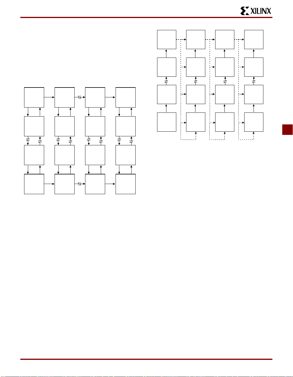
The carry chain in XC4000E devices can run either up or
down. At the top and bottom of the columns where there
are no CLBs above or below, the carry is propagated to the
right. (See Figure 12.) In order to improve speed in the
high-capacity XC4000X devices, which can potentially
have very long carry chains, the carry chain travels upward
only, as shown in Figure 13. Additionally, standard interconnect can be used to route a carry signal in the downward direction.
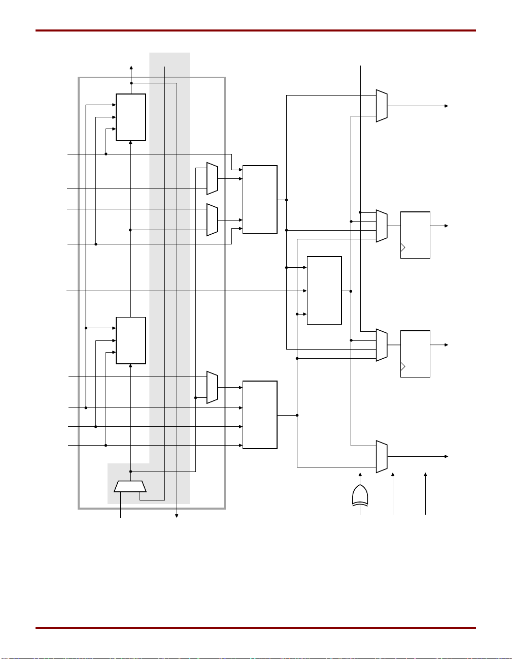
Figure 14 on page 4-20 shows an XC4000E CLB with ded-
icated fast carry logic. The carry logic in the XC4000X is
similar, except that COUT exits at the top only , and the signal CINDOWN does not exist. As shown in Figure 14, the
carry logic shares operand and control inputs with the function generators. The carry outputs connect to the function
generators, where they are combined with the operands to
form the sums.
Figure 15 on page 4-21 shows the details of the carry logic
for the XC4000E. This diagram shows the contents of the
box labeled “CARRY LOGIC” in Figure 14. The XC4000X
carry logic is very similar, but a multiplexer on the passthrough carry chain has been eliminated to reduce delay.
Additionally , in the XC4000X the multiple x er on the G4 path
has a memory-programmable 0 input, which permits G4 to
4-18 March 30, 1998 (Version 1.5)
Page 19
directly connect to COUT. G4 thus becomes an additional
high-speed initialization path for carry-in.
The dedicated carry logic is discussed in detail in Xilinx
document XAPP 013: “
XC4000
.” This discussion also applies to XC4000E
Using the Dedicated Carry Logic in
devices, and to XC4000X devices when the minor logic
changes are taken into account.
The fast carry logic can be accessed by placing special
library symbols, or by using Xilinx Relationally Placed Macros (RPMs) that already include these symbols.
CLB CLB CLB CLB
CLB
CLB
CLB
CLB
CLB CLB CLB CLB
CLB
CLB
CLB
CLB
CLB
CLB
CLB
CLB
CLB CLB CLB CLB
Figure 12: Available XC4000E Carry Propagation
Paths
X6687
CLB
CLB
CLB
CLB
CLB CLB CLB CLB
X6610
Figure 13: Available XC4000X Carry Propagation
Paths (dotted lines use general interconnect)
March 30, 1998 (Version 1.5) 4-19
Page 20
XC4000E and XC4000X Series Field Programmable Gate Arrays
H1
G4
G3
G2
G1
CARRY
LOGIC
C
OUT
G
CARRY
C
F
CARRY
OUT0
C
IN
DOWN
G
H
D
IN
G
Y
YQ
XQ
DIN
DIN
H
H
G
F
H
G
F
S/R
DQ
EC
S/R
DQ
F4
F3
F2
F1
CC
IN
UP
OUT
F
H
F
K S/R EC
EC
X
X6699
Figure 14: Fast Carry Logic in XC4000E CLB (shaded area not present in XC4000X)
4-20 March 30, 1998 (Version 1.5)
Page 21

C
OUT
G1
G4
M
1
01
0
I
M
G2
F2
F1
M
01
F3
M
X2000
M
Figure 15: Detail of XC4000E Dedicated Carry Logic
Input/Output Blocks (IOBs)
User-configurable input/output blocks (IOBs) provide the
interface between external package pins and the internal
logic. Each IOB controls one package pin and can be configured for input, output, or bidirectional signals.
Figure 16 shows a simplified block diagram of the
XC4000E IOB. A more complete diagram which includes
the boundary scan logic of the XC4000E IOB can be found
in Figure 41 on page 4-44, in the “Boundary Scan” section.
The XC4000X IOB contains some special features not
included in the XC4000E IOB. These features are highlighted in a simplified block diagram f ound inFigure 17, and
discussed throughout this section. When XC4000X special
features are discussed, they are clearly identified in the
text. Any feature not so identified is present in both
XC4000E and XC4000X devices.
IOB Input Signals
Two paths, labeled I1 and I2 in Figure 16 and Figure 17,
bring input signals into the array. Inputs also connect to an
input register that can be programmed as either an edgetriggered flip-flop or a level-sensitive latch.
OUT0
IN DOWN
G3
TO
FUNCTION
M
F4
M
GENERATORS
C
M
1
0
M
3
1
0
01
M
M
10
C
INUP
C
The choice is made by placing the appropriate library symbol. For example, IFD is the basic input flip-flop (rising edge
triggered), and ILD is the basic input latch (transparentHigh). Variations with inverted clocks are available, and
some combinations of latches and flip-flops can be implemented in a single IOB, as described in the
Guide
.
XACT Libraries
The XC4000E inputs can be globally configured for either
TTL (1.2V) or 5.0 volt CMOS thresholds, using an option in
the bitstream generation software. There is a slight input
hysteresis of about 300mV. The XC4000E output lev els are
also configurable; the two global adjustments of input
threshold and output level are independent.
Inputs on the XC4000XL are TTL compatible and 3.3V
CMOS compatible. Outputs on the XC4000XL are pulled to
the 3.3V positive supply.
The inputs of XC4000 Series 5-Volt devices can be driven
by the outputs of any 3.3-V olt de vice , if the 5-Volt inputs are
in TTL mode.
Supported sources for XC4000 Series device inputs are
shown in Table 9.
March 30, 1998 (Version 1.5) 4-21
Page 22
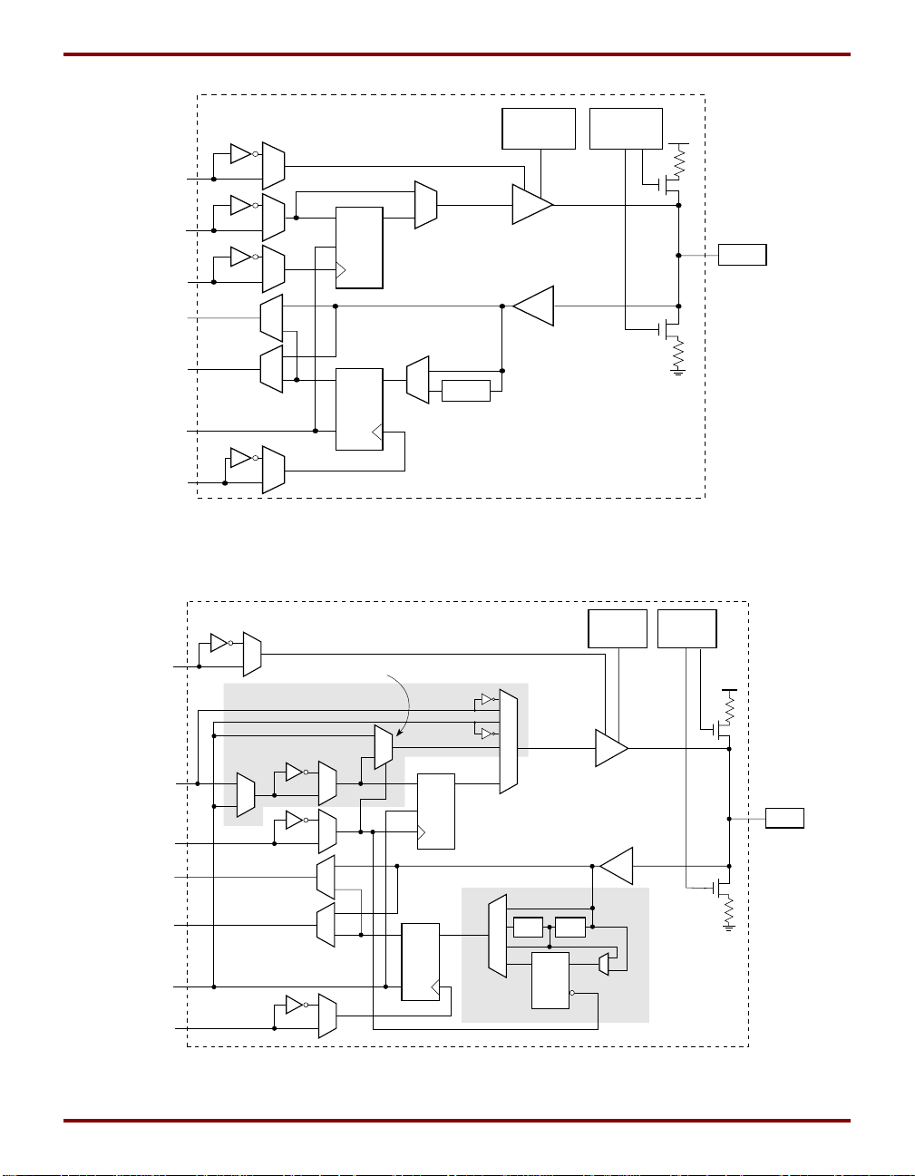
XC4000E and XC4000X Series Field Programmable Gate Arrays
T
Flip-Flop
Q
Out
D
CE
Output
Clock
I
Clock
Enable
Input
Clock
1
I
2
Flip-
Flop/
Latch
Q
CE
D
Figure 16: Simplified Block Diagram of XC4000E IOB
T
Output MUX
Delay
Slew Rate
Control
Input
Buffer
Pull-Down
Output
Buffer
Slew Rate
Passive
Pull-Up/
Control
Passive
Pull-Up/
Pull-Down
Pad
X6704
0
1
Out
Output Clock
Clock Enable
Input Clock
I
1
I
2
Flip-Flop
D
CE
Flip-Flop/
Latch
Q
D
CE
Q
Delay Delay
Q
Latch
Fast
Capture
Latch
Output
Buffer
Input
Buffer
D
G
Pad
X5984
Figure 17: Simplified Block Diagram of XC4000X IOB (shaded areas indicate differences from XC4000E)
4-22 March 30, 1998 (Version 1.5)
Page 23

Table 9: Supported Sources for XC4000 Series Device
Inputs
Source
Any device, Vcc = 3.3 V,
CMOS outputs
XC4000 Series, Vcc = 5 V,
TTL outputs
Any device, Vcc = 5 V,
TTL outputs (Voh ≤ 3.7 V)
Any device, Vcc = 5 V,
CMOS outputs
XC4000E/EX
Series Inputs
5 V,
TTL
CMOS
√
Unreli
-able
√√
√√
√√ √
5 V,
Data
XC4000XL
Series Inputs
3.3 V
CMOS
√
XC4000XL 5-Volt Tolerant I/Os
The I/Os on the XC4000XL are fully 5-volt tolerant even
though the VCC is 3.3 volts. This allows 5 V signals to
directly connect to the XC4000XL inputs without damage,
as shown in Table 9. In addition, the 3.3 volt VCC can be
applied before or after 5 volt signals are applied to the I/Os.
This makes the XC4000XL immune to power supply
sequencing problems.
Registered Inputs
The I1 and I2 signals that exit the block can each carry
either the direct or registered input signal.
The input and output storage elements in each IOB have a
common clock enable input, which, through configuration,
can be activated individually for the input or output flip-flop,
or both. This clock enable operates exactly like the EC pin
on the XC4000 Series CLB. It cannot be inverted within the
IOB.
The storage element behavior is shown in Table 10.
Table 10: Input Register Functionality
(active rising edge is shown)
Mode Clock
Power-Up or
XXXSR
Clock
Enable
DQ
GSR
Flip-Flop __/ 1* D D
0XXQ
Latch 1 1* X Q
01*DD
Both X 0 X Q
Legend:
__/
SR
0*
1*
X
Don’t care
Rising edge
Set or Reset value. Reset is default.
Input is Low or unconnected (default value)
Input is High or unconnected (default value)
Optional Delay Guarantees Zero Hold Time
The data input to the register can optionally be delayed by
several nanoseconds. With the delay enabled, the setup
time of the input flip-flop is increased so that normal clock
routing does not result in a positive hold-time requirement.
A positive hold time requirement can lead to unreliable,
temperature- or processing-dependent operation.
The input flip-flop setup time is defined between the data
measured at the device I/O pin and the clock input at the
IOB (not at the clock pin). Any routing delay from the de vice
clock pin to the clock input of the IOB must, therefore, be
subtracted from this setup time to arrive at the real setup
time requirement relative to the device pins. A short specified setup time might, therefore, result in a negative setup
time at the device pins, i.e., a positive hold-time requirement.
When a delay is inserted on the data line, more clock delay
can be tolerated without causing a positive hold-time
requirement. Sufficient delay eliminates the possibility of a
data hold-time requirement at the external pin. The maximum delay is therefore inserted as the default.
The XC4000E IOB has a one-tap delay element: either the
delay is inserted (default), or it is not. The delay guarantees
a zero hold time with respect to clocks routed through any
of the XC4000E global clock buffers . (See“Global Nets and
Buffers (XC4000E only)” on page 4-36 for a description of
the global clock buffers in the XC4000E.) For a shorter
input register setup time, with non-zero hold, attach a
NODELAY attribute or property to the flip-flop.
The XC4000X IOB has a two-tap delay element, with
choices of a full delay, a partial delay, or no delay. The
attributes or properties used to select the desired delay are
shown in Ta b l e 1 1 . The choices are no added attribute,
MEDDELAY, and NODELAY. The default setting, with no
added attribute, ensures no hold time with respect to any of
the XC4000X clock buffers , including the Global Low-Skew
buffers. MEDDELAY ensures no hold time with respect to
the Global Early buffers. Inputs with NODELAY may hav e a
positive hold time with respect to all clock buffers. For a
description of each of these buffers, see “Global Nets and
Buffers (XC4000X only)” on page 4-38.
Table 11: XC4000X IOB Input Delay Element
Value When to Use
full delay
(default, no
Zero Hold with respect to Global LowSkew Buffer, Global Early Buffer
attribute added)
MEDDELAY Zero Hold with respect to Global Early
Buffer
NODELAY Short Setup, positive Hold time
March 30, 1998 (Version 1.5) 4-23
Page 24
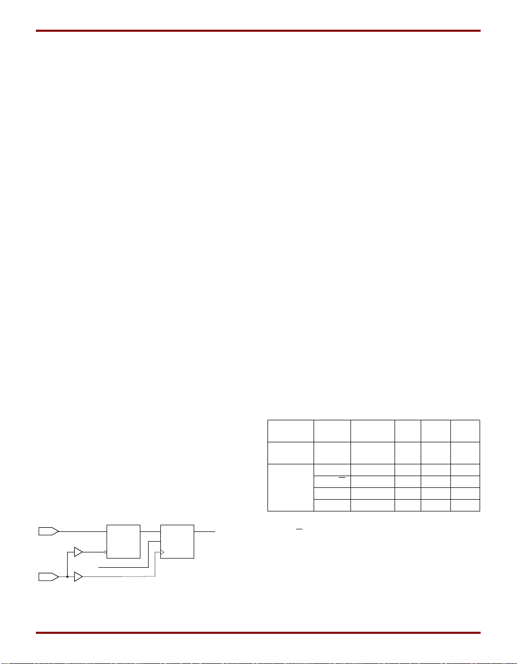
XC4000E and XC4000X Series Field Programmable Gate Arrays
Additional Input Latch for Fast Capture (XC4000X only)
The XC4000X IOB has an additional optional latch on the
input. This latch, as shown in Figure 17, is clocked by the
output clock — the clock used for the output flip-flop —
rather than the input clock. Therefore, two different clocks
can be used to clock the two input storage elements. This
additional latch allows the very fast capture of input data,
which is then synchronized to the internal clock by the IOB
flip-flop or latch.
To use this Fast Capture technique, drive the output clock
pin (the Fast Capture latching signal) from the output of one
of the Global Early buffers supplied in the XC4000X. The
second storage element should be clocked by a Global
Low-Skew buffer, to synchronize the incoming data to the
internal logic. (See Figure 18.) These special buffers are
described in “Global Nets and Buffers (XC4000X only)” on
page 4-38.
The Fast Capture latch (FCL) is designed primarily for use
with a Global Early buffer. For Fast Capture, a single clock
signal is routed through both a Global Early buffer and a
Global Low-Skew buffer. (The two buffers share an input
pad.) The Fast Capture latch is clock ed b y the Global Early
buffer, and the standard IOB flip-flop or latch is clocked by
the Global Low-Skew buffer. This mode is the safest way to
use the Fast Capture latch, because the clock buffers on
both storage elements are driven by the same pad. There
is no external skew between clock pads to create potential
problems.
To place the Fast Capture latch in a design, use one of the
special library symbols, ILFFX or ILFLX. ILFFX is a transparent-Low Fast Capture latch followed by an active-High
input flip-flop. ILFLX is a transparent-Low Fast Capture
latch followed by a transparent-High input latch. Any of the
clock inputs can be inverted before driving the library element, and the inverter is absorbed into the IOB. If a single
BUFG output is used to drive both clock inputs, the software automatically runs the clock through both a Global
Low-Skew buffer and a Global Early buffer, and clocks the
Fast Capture latch appropriately.
Figure 17 on page 4-22 also shows a two-tap delay on the
input. By default, if the Fast Capture latch is used, the Xilinx
software assumes a Global Early buffer is driving the clock,
and selects MEDDELAY to ensure a zero hold time. Select
ILFFX
IPAD
IPAD
BUFGE
BUFGLS
DQ
GF
CE
C
Figure 18: Examples Using XC4000X FCL
to internal
logic
X9013
the desired delay based on the discussion in the previous
subsection.
IOB Output Signals
Output signals can be optionally inverted within the IOB,
and can pass directly to the pad or be stored in an edgetriggered flip-flop. The functionality of this flip-flop is shown
in Table 12.
An active-High 3-state signal can be used to place the output buffer in a high-impedance state, implementing 3-state
outputs or bidirectional I/O. Under configuration control, the
output (OUT) and output 3-state (T) signals can be
inverted. The polarity of these signals is independently configured for each IOB.
The 4-mA maximum output current specification of many
FPGAs often forces the user to add external buffers, which
are especially cumbersome on bidirectional I/O lines. The
XC4000E and XC4000EX/XL devices solve many of these
problems by providing a guaranteed output sink current of
12 mA. Two adjacent outputs can be interconnected externally to sink up to 24 mA. The XC4000E and XC4000EX/XL
FPGAs can thus directly drive buses on a printed circuit
board.
By default, the output pull-up structure is configured as a
TTL-like totem-pole. The High driver is an n-channel pullup transistor, pulling to a voltage one transistor threshold
below Vcc. Alternatively , the outputs can be globally configured as CMOS drivers, with p-channel pull-up transistors
pulling to Vcc. This option, applied using the bitstream generation software, applies to all outputs on the device. It is
not individually programmable. In the XC4000XL, all outputs are pulled to the positive supply rail.
Table 12: Output Flip-Flop Functionality (active rising
edge is shown)
Clock
Mode Clock
Power-Up
or GSR
Flip-Flop
Legend:
X
Don’t care
__/
Rising edge
SR
Set or Reset value. Reset is default.
0*
Input is Low or unconnected (default value)
1*
Input is High or unconnected (default value)
Z
3-state
__/ 1* 0* D D
Enable T D Q
X X 0* X SR
X00*XQ
XX1XZ
0X0*XQ
4-24 March 30, 1998 (Version 1.5)
Page 25
Any XC4000 Series 5-Volt device with its outputs configured in TTL mode can drive the inputs of any typical 3.3Volt device. (For a detailed discussion of how to interface
between 5 V and 3.3 V devices, see the 3V Products section of
The Programmable Logic Data Book
.)
Supported destinations for XC4000 Series device outputs
are shown in Table 13.
An output can be configured as open-drain (open-collector)
by placing an OBUFT symbol in a schematic or HDL code,
then tying the 3-state pin (T) to the output signal, and the
input pin (I) to Ground. (See Figure 19.)
Table 13: Supported Destinations for XC4000 Series
Outputs
XC4000 Series
Outputs
Destination
Any typical device, Vcc = 3.3 V,
3.3 V,
CMOS
5 V,
TTL
√√some
5 V,
CMOS
CMOS-threshold inputs
Any device, Vcc = 5 V,
√√√
TTL-threshold inputs
Any device, Vcc = 5 V,
CMOS-threshold inputs
1. Only if destination device has 5-V tolerant inputs
OBUFT
Unreliable
Data
OPAD
X6702
√
Figure 19: Open-Drain Output
Output Slew Rate
The slew rate of each output buffer is, by default, reduced,
to minimize power bus transients when switching non-critical signals. For critical signals, attach a FAST attribute or
property to the output buffer or flip-flop.
For XC4000E devices, maximum total capacitive load for
simultaneous fast mode switching in the same direction is
200 pF for all package pins between each Power/Ground
pin pair. For XC4000X devices, additional internal Power/
Ground pin pairs are connected to special Power and
Ground planes within the packages, to reduce ground
bounce. Therefore, the maximum total capacitive load is
300 pF between each external Power/Ground pin pair.
Maximum loading may vary for the low-voltage devices.
For slew-rate limited outputs this total is two times larger f or
each device type: 400 pF for XC4000E de vices and 600 pF
for XC4000X devices. This maximum capacitive load
should not be exceeded, as it can result in ground bounce
of greater than 1.5 V amplitude and more than 5 ns duration. This level of ground bounce may cause undesired
transient behavior on an output, or in the internal logic. This
restriction is common to all high-speed digital ICs, and is
not particular to Xilinx or the XC4000 Series.
XC4000 Series devices have a feature called “Soft Startup,” designed to reduce ground bounce when all outputs
are turned on simultaneously at the end of configuration.
When the configuration process is finished and the device
1
starts up, the first activation of the outputs is automatically
slew-rate limited. Immediately following the initial activ ation
of the I/O, the slew rate of the individual outputs is determined by the individual configuration option for each IOB.
Global Three-State
A separate Global 3-State line (not shown in Figure 16 or
Figure 17) forces all FPGA outputs to the high-impedance
state, unless boundary scan is enabled and is executing an
EXTEST instruction. This global net (GTS) does not compete with other routing resources; it uses a dedicated distribution network.
GTS can be driven from any user-programmable pin as a
global 3-state input. To use this global net, place an input
pad and input buffer in the schematic or HDL code, driving
the GTS pin of the STARTUP symbol. A specific pin location can be assigned to this input using a LOC attribute or
property, just as with any other user-prog rammable pad. An
inverter can optionally be inserted after the input buffer to
invert the sense of the Global 3-State signal. Using GTS is
similar to GSR. See Figure 3 on page 4-11 for details.
Alternatively, GTS can be driven from any internal node.
March 30, 1998 (Version 1.5) 4-25
Page 26
XC4000E and XC4000X Series Field Programmable Gate Arrays
Output Multiplexer/2-Input Function Generator
(XC4000X only)
As shown in Figure 17 on page 4-22, the output path in the
XC4000X IOB contains an additional multiplexer not available in the XC4000E IOB. The multiplexer can also be configured as a 2-input function generator, implementing a
pass-gate, AND-gate, OR-gate, or XOR-gate, with 0, 1, or
2 inverted inputs. The logic used to implement these functions is shown in the upper gray area of Figure 17.
When configured as a multiplexer, this feature allows two
output signals to time-share the same output pad; effectively doubling the number of de vice outputs without requiring a larger, more expensive package.
When the MUX is configured as a 2-input function generator, logic can be implemented within the IOB itself. Combined with a Global Early buffer, this arrangement allows
very high-speed gating of a single signal. For example, a
wide decoder can be implemented in CLBs, and its output
gated with a Read or Write Strobe Driven by a BUFGE
buffer, as shown in Figure 20. The critical-path pin-to-pin
delay of this circuit is less than 6 nanoseconds.
As shown in Figure 17, the IOB input pins Out, Output
Clock, and Clock Enable hav e different delays and different
flexibilities regarding polarity. Additionally, Output Clock
sources are more limited than the other inputs. Therefore,
the Xilinx software does not move logic into the IOB function generators unless explicitly directed to do so.
The user can specify that the IOB function generator be
used, by placing special library symbols beginning with the
letter “O.” For example , a 2-input AND-gate in the IOB function generator is called OAND2. Use the symbol input pin
labelled “F” for the signal on the critical path. This signal is
placed on the OK pin — the IOB input with the shortest
delay to the function generator . Two e xamples are shown in
Figure 21.
IPAD
BUFGE
from
internal
logic
F
OAND2
OPAD
FAST
X9019
Figure 20: Fast Pin-to-Pin Path in XC4000X
OMUX2
F
OAND2
X6598
D0
D1
S0
O
X6599
Figure 21: AND & MUX Symbols in XC4000X IOB
Other IOB Options
There are a number of other programmable options in the
XC4000 Series IOB.
Pull-up and Pull-down Resistors
Programmable pull-up and pull-down resistors are useful
for tying unused pins to Vcc or Ground to minimize power
consumption and reduce noise sensitivity . The configurab le
pull-up resistor is a p-channel transistor that pulls to Vcc.
The configurable pull-down resistor is an n-channel transistor that pulls to Ground.
The value of these resistors is 50 kΩ − 100 kΩ. This high
value makes them unsuitable as wired-AND pull-up resistors.
The pull-up resistors for most user-programmable IOBs are
active during the configuration process. See Table 23 on
page 4-59 for a list of pins with pull-ups active before and
during configuration.
After configuration, voltage levels of unused pads, bonded
or unbonded, must be valid logic levels, to reduce noise
sensitivity and avoid excess current. Therefore, by default,
unused pads are configured with the internal pull-up resistor active. Alternatively, they can be individually configured
with the pull-down resistor, or as a driven output, or to be
driven by an external source. To activate the internal pullup, attach the PULLUP library component to the net
attached to the pad. To activate the internal pull-down,
attach the PULLDOWN library component to the net
attached to the pad.
Independent Clocks
Separate clock signals are provided for the input and output flip-flops. The clock can be independently inverted for
each flip-flop within the IOB, generating either falling-edge
or rising-edge triggered flip-flops. The clock inputs for each
IOB are independent, except that in the XC4000X, the Fast
Capture latch shares an IOB input with the output clock pin.
Early Clock for IOBs (XC4000X only)
Special early clocks are available for IOBs. These clocks
are sourced by the same sources as the Global Low-Skew
buffers, b ut are separ ately buffered. They have fewer loads
and therefore less delay. The early clock can drive either
the IOB output clock or the IOB input clock, or both. The
early clock allows fast capture of input data, and f ast clockto-output on output data. The Global Early buffers that drive
these clocks are described in “Global Nets and Buffers
(XC4000X only)” on page 4-38.
Global Set/Reset
As with the CLB registers, the Global Set/Reset signal
(GSR) can be used to set or clear the input and output registers, depending on the value of the INIT attribute or property. The two flip-flops can be individually configured to set
4-26 March 30, 1998 (Version 1.5)
Page 27

or clear on reset and after configuration. Other than the global GSR net, no user-controlled set/reset signal is available
to the I/O flip-flops. The choice of set or clear applies to
both the initial state of the flip-flop and the response to the
Global Set/Reset pulse. See “Global Set/Reset” on page 4-
11 for a description of how to use GSR.
JTAG Support
Embedded logic attached to the IOBs contains test structures compatible with IEEE Standard 1149.1 for boundary
scan testing, permitting easy chip and board-level testing.
More information is provided in “Boundary Scan” on
page 4-43.
Three-State Buffers
A pair of 3-state buffers is associated with each CLB in the
array. (See Figure 28 on page 4-31.) These 3-state buffers
can be used to drive signals onto the nearest horizontal
longlines above and below the CLB. They can therefore be
used to implement multiplexed or bidirectional b uses on the
horizontal longlines, saving logic resources. Programmab le
pull-up resistors attached to these longlines help to implement a wide wired-AND function.
The buffer enable is an active-High 3-state (i.e. an activeLow enable), as shown in Table 14.
Another 3-state buffer with similar access is located near
each I/O block along the right and left edges of the array.
(See Figure 34 on page 4-35.)
The horizontal longlines driven by the 3-state buffers have
a weak keeper at each end. This circuit prevents undefined
floating levels. Ho w ever, it is overridden by any driver, e ven
a pull-up resistor.
Special longlines running along the perimeter of the array
can be used to wire-AND signals coming from nearby IOBs
or from internal longlines. These longlines form the wide
edge decoders discussed in “Wide Edge Decoders” on
page 4-28.
Three-State Buffer Modes
The 3-state buffers can be configured in three modes:
• Standard 3-state buffer
• Wired-AND with input on the I pin
• Wired OR-AND
Standard 3-State Buffer
All three pins are used. Place the library element BUFT.
Connect the input to the I pin and the output to the O pin.
The T pin is an active-High 3-state (i.e. an active-Low
enable). Tie the T pin to Ground to implement a standard
buffer.
Wired-AND with Input on the I Pin
The buffer can be used as a Wired-AND. Use the WAND1
library symbol, which is essentially an open-drain buffer.
WAND4, WAND8, and WAND16 are also available. See
the
XACT Libraries Guide
for further information.
The T pin is internally tied to the I pin. Connect the input to
the I pin and the output to the O pin. Connect the outputs of
all the WAND1s together and attach a PULLUP symbol.
Wired OR-AND
The buffer can be configured as a Wired OR-AND. A High
level on either input turns off the output. Use the
WOR2AND library symbol, which is essentially an opendrain 2-input OR gate. The two input pins are functionally
equivalent. Attach the two inputs to the I0 and I1 pins and
tie the output to the O pin. Tie the outputs of all the
WOR2ANDs together and attach a PULLUP symbol.
Three-State Buffer Examples
Figure 22 shows how to use the 3-state buffers to imple-
ment a wired-AND function. When all the buffer inputs are
High, the pull-up resistor(s) provide the High output.
Figure 23 shows how to use the 3-state buffers to imple-
ment a multiplexer. The selection is accomplished by the
buffer 3-state signal.
Pay particular attention to the polarity of the T pin when
using these buffers in a design. Active-High 3-state (T) is
identical to an active-Low output enable, as shown in
Ta bl e 1 4.
Table 14: Three-State Buffer Functionality
IN T OUT
X1Z
IN 0 IN
● DB ● (D
Z = D
A
D
D
A
WAND1 WAND1
D
B
C
D
D
) ● (DE+DF)
C+DD
D
E
D
WOR2AND WOR2AND
F
P
U
U
L
P
L
X6465
Figure 22: Open-Drain Buffers Implement a Wired-AND Function
March 30, 1998 (Version 1.5) 4-27
Page 28
XC4000E and XC4000X Series Field Programmable Gate Arrays
~100 k
Ω
Z = D
• A + DB • B + DC • C + DN • N
A
D
A
BUFT BUFT BUFT BUFT
ABCN
"Weak Keeper"
Figure 23: 3-State Buffers Implement a Multiplexer
Wide Edge Decoders
Dedicated decoder circuitry boosts the performance of
wide decoding functions. When the address or data field is
wider than the function generator inputs, FPGAs need
multi-level decoding and are thus slower than PALs.
XC4000 Series CLBs have nine inputs. Any decoder of up
to nine inputs is, therefore, compact and fast. However,
there is also a need for much wider decoders, especially for
address decoding in large microprocessor systems.
An XC4000 Series FPGA has four programmable decoders
located on each edge of the device. The inputs to each
decoder are any of the IOB I1 signals on that edge plus one
local interconnect per CLB row or column. Each row or column of CLBs provides up to three variables or their compliments., as shown in Figure 24. Each decoder generates a
High output (resistor pull-up) when the AND condition of
the selected inputs, or their complements, is true. This is
analogous to a product term in typical PAL devices.
Each of these wired-AND gates is capable of accepting up
to 42 inputs on the XC4005E and 72 on the XC4013E.
There are up to 96 inputs for each decoder on the
XC4028X and 132 on the XC4052X. The decoders may
also be split in two when a larger number of narrower
decoders are required, for a maximum of 32 decoders per
device.
The decoder outputs can drive CLB inputs, so they can be
combined with other logic to form a P AL-lik e AND/OR structure. The decoder outputs can also be routed directly to the
chip outputs. For fastest speed, the output should be on the
same chip edge as the decoder. Very large PALs can be
emulated by ORing the decoder outputs in a CLB. This
decoding feature covers what has long been considered a
weakness of older FPGAs. Users often resorted to external
PALs for simple but fast decoding functions. Now, the dedicated decoders in the XC4000 Series device can implement these functions fast and efficiently.
To use the wide edge decoders, place one or more of the
WAND library symbols (WAND1, WAND4, WAND8,
WAND16). Attach a DECODE attribute or property to each
WAND symbol. Tie the outputs together and attach a PUL-
D
B
D
C
D
N
X6466
LUP symbol. Location attributes or properties such as L
(left edge) or TR (right half of top edge) should also be used
to ensure the correct placement of the decoder inputs.
INTERCONNECT
IOB
C
IOB
.I1.I1
BA
Figure 24: XC4000 Series Edge Decoding Example
OSC4
F8M
F500K
F16K
F490
F15
X6703
Figure 25: XC4000 Series Oscillator Symbol
On-Chip Oscillator
XC4000 Series devices include an internal oscillator. This
oscillator is used to clock the power-on time-out, for configuration memory clearing, and as the source of CCLK in
Master configuration modes. The oscillator runs at a nominal 8 MHz frequency that varies with process, Vcc, and
temperature. The output frequency falls between 4 and 10
MHz.
( C) .....
(A • B • C) .....
(A • B • C) .....
(A • B • C) .....
X2627
4-28 March 30, 1998 (Version 1.5)
Page 29

The oscillator output is optionally available after configuration. Any two of four resynchronized taps of a built-in
divider are also available. These taps are at the fourth,
ninth, fourteenth and nineteenth bits of the divider. Therefore, if the primary oscillator output is running at the nominal 8 MHz, the user has access to an 8 MHz clock, plus any
two of 500 kHz, 16kHz, 490Hz and 15Hz (up to 10% lower
for low-voltage devices). These frequencies can vary by as
much as -50% or +25%.
These signals can be accessed by placing the OSC4
library element in a schematic or in HDL code (see
Figure 25).
The oscillator is automatically disabled after configuration if
the OSC4 symbol is not used in the design.
Programmable Interconnect
All internal connections are composed of metal segments
with programmable switching points and switching matrices to implement the desired routing. A structured, hierarchical matrix of routing resources is provided to achieve
efficient automated routing.
The XC4000E and XC4000X share a basic interconnect
structure. XC4000X devices, however, have additional
routing not available in the XC4000E. The extra routing
resources allow high utilization in high-capacity devices. All
XC4000X-specific routing resources are clearly identified
throughout this section. Any resources not identified as
XC4000X-specific are present in all XC4000 Series
devices.
This section describes the varied routing resources available in XC4000 Series devices. The implementation software automatically assigns the appropriate resources
based on the density and timing requirements of the
design.
Interconnect Overview
There are several types of interconnect.
• CLB routing is associated with each row and column of
the CLB array.
• IOB routing forms a ring (called a VersaRing) around
the outside of the CLB array. It connects the I/O with the
internal logic blocks.
• Global routing consists of dedicated networks primarily
designed to distribute clocks throughout the device with
minimum delay and skew. Global routing can also be
used for other high-fanout signals.
Five interconnect types are distinguished by the relative
length of their segments: single-length lines, double-length
lines, quad and octal lines (XC4000X only), and longlines.
In the XC4000X, direct connects allow fast data flow
between adjacent CLBs, and between IOBs and CLBs.
Extra routing is included in the IOB pad ring. The XC4000X
also includes a ring of octal interconnect lines near the
IOBs to improve pin-swapping and routing to locked pins.
XC4000E/X devices include two types of global buffers.
These global buffers have different properties, and are
intended for different purposes. They are discussed in
detail later in this section.
CLB Routing Connections
A high-level diagram of the routing resources associated
with one CLB is shown in Figure 26. The shaded arrows
represent routing present only in XC4000X devices.
Table 15 shows how much routing of each type is available
in XC4000E and XC4000X CLB arrays. Clearly, very large
designs, or designs with a great deal of interconnect, will
route more easily in the XC4000X. Smaller XC4000E
designs, typically requiring significantly less interconnect,
do not require the additional routing.
Figure 28 on page 4-31 is a detailed diagram of both the
XC4000E and the XC4000X CLB, with associated routing.
The shaded square is the programmable switch matrix,
present in both the XC4000E and the XC4000X. The Lshaped shaded area is present only in XC4000X devices.
As shown in the figure, the XC4000X block is essentially an
XC4000E block with additional routing.
CLB inputs and outputs are distributed on all four sides,
providing maximum routing flexibility. In general, the entire
architecture is symmetrical and regular. It is well suited to
established placement and routing algorithms. Inputs, outputs, and function generators can freely swap positions
within a CLB to avoid routing congestion during the placement and routing operation.
March 30, 1998 (Version 1.5) 4-29
Page 30
XC4000E and XC4000X Series Field Programmable Gate Arrays
Quad
Single
Double
Long
Direct
Connect
Long
x5994
Quad
Long Global
Clock
Long Double Single Global
Clock
Carry
Chain
CLB
Direct
Connect
Figure 26: High-Level Routing Diagram of XC4000 Series CLB (shaded arrows indicate XC4000X only)
Table 15: Routing per CLB in XC4000 Series Devices
XC4000E XC4000X
Double
Singles
Double
Vertical Horizontal Vertical Horizontal
Singles 8 8 8 8
Doubles 4 4 4 4
Quads 0 0 12 12
Longlines 6 6 10 6
Direct
0022
Connects
Double
Singles
Double
Six Pass Transistors
Per Switch Matrix
Interconnect Point
Globals 4 0 8 0
Carry Logic 2 0 1 0
Total 24 18 45 32
Programmable Switch Matrices
The horizontal and vertical single- and double-length lines
intersect at a box called a programmable switch matrix
(PSM). Each switch matrix consists of programmable pass
transistors used to establish connections between the lines
(see Figure 27).
For example, a single-length signal entering on the right
side of the switch matrix can be routed to a single-length
line on the top, left, or bottom sides, or any combination
thereof, if multiple branches are required. Similarly, a double-length signal can be routed to a double-length line on
any or all of the other three edges of the programmable
switch matrix.
Figure 27: Programmable Switch Matrix (PSM)
Single-Length Lines
Single-length lines provide the greatest interconnect flexibility and offer fast routing between adjacent blocks. There
are eight vertical and eight horizontal single-length lines
associated with each CLB. These lines connect the switching matrices that are located in every row and a column of
CLBs.
Single-length lines are connected by way of the programmable switch matrices, as shown in Figure 29. Routing
connectivity is shown in Figure 28.
Single-length lines incur a delay whenever they go through
a switching matrix. Therefore, they are not suitable for routing signals for long distances. They are normally used to
conduct signals within a localized area and to provide the
branching for nets with fanout greater than one.
X6600
4-30 March 30, 1998 (Version 1.5)
Page 31

QUAD
DOUBLE
SINGLE
DOUBLE
LONG
F4
C4
G4
YQ
Y
G1
C1
F1
G3
CLB
C3
F3
K
X
XQ
G2
F2
C2
DIRECT
FEEDBACK
LONG
GLOBAL
QUAD
LONG
GLOBAL
LONG
DOUBLE
SINGLE
LONG
DOUBLE
DIRECT
FEEDBACK
Common to XC4000E and XC4000X
XC4000X only
Programmable Switch Matrix
Figure 28: Detail of Programmable Interconnect Associated with XC4000 Series CLB
March 30, 1998 (Version 1.5) 4-31
Page 32

XC4000E and XC4000X Series Field Programmable Gate Arrays
CLB
PSM PSM
CLB CLB CLB
CLB CLB CLB
CLB CLB
Doubles
Singles
Doubles
PSMPSM
X6601
Figure 29: Single- and Double-Length Lines, with
Programmable Switch Matrices (PSMs)
Double-Length Lines
The double-length lines consist of a grid of metal segments, each twice as long as the single-length lines: they
run past two CLBs before entering a switch matrix. Doublelength lines are grouped in pairs with the switch matrices
staggered, so that each line goes through a switch matrix at
every other row or column of CLBs (see Figure 29).
There are four vertical and four horizontal double-length
lines associated with each CLB. These lines provide faster
signal routing over intermediate distances, while retaining
routing flexibility. Double-length lines are connected by wa y
of the programmable switch matrices. Routing connectivity
is shown in Figure 28.
Quad Lines (XC4000X only)
XC4000X devices also include twelve vertical and twelve
horizontal quad lines per CLB row and column. Quad lines
are four times as long as the single-length lines. They are
interconnected via buffered switch matrices (shown as diamonds in Figure 28 on page 4-31). Quad lines run past four
CLBs before entering a buffered switch matrix. They are
grouped in fours, with the buffered switch matrices staggered, so that each line goes through a buffered switch
matrix at every fourth CLB location in that row or column.
(See Figure 30.)
The buffered switch matrixes have four pins, one on each
edge. All of the pins are bidirectional. Any pin can drive any
or all of the other pins.
Each buffered switch matrix contains one buffer and six
pass transistors. It resembles the programmable switch
matrix shown in Figure 27, with the addition of a programmable buffer. There can be up to two independent inputs
CLB
CLB
CLB
CLB
CLB
CLB
CLB
CLB
CLB
X9014
Figure 30: Quad Lines (XC4000X only)
and up to two independent outputs. Only one of the independent inputs can be buffered.
The place and route software automatically uses the timing
requirements of the design to determine whether or not a
quad line signal should be buffered. A heavily loaded signal
is typically buffered, while a lightly loaded one is not. One
scenario is to alternate buffers and pass transistors. This
allows both vertical and horizontal quad lines to be buffered
at alternating buffered switch matrices.
Due to the buffered switch matrices, quad lines are very
fast. They provide the fastest available method of routing
heavily loaded signals for long distances across the de vice.
Longlines
Longlines form a grid of metal interconnect segments that
run the entire length or width of the array. Longlines are
intended for high fan-out, time-critical signal nets, or nets
that are distributed over long distances. In XC4000X
devices, quad lines are preferred for critical nets, because
the buffered switch matrices make them faster for high fanout nets.
Two horizontal longlines per CLB can be driven by 3-state
or open-drain drivers (TBUFs). They can therefore implement unidirectional or bidirectional buses, wide multiplexers, or wired-AND functions. (See “Three-State Buffers” on
page 4-27 for more details.)
Each horizontal longline driven by TBUFs has either two
(XC4000E) or eight (XC4000X) pull-up resistors. To activate these resistors, attach a PULLUP symbol to the longline net. The software automatically activates the appropriate number of pull-ups. There is also a weak keeper at
each end of these two horizontal longlines. This circuit pre-
4-32 March 30, 1998 (Version 1.5)
Page 33
vents undefined floating levels . Ho w e ver, it is overridden b y
any driver, even a pull-up resistor.
Each XC4000E longline has a programmable splitter
switch at its center, as does each XC4000X longline driven
by TBUFs. This switch can separate the line into two independent routing channels, each running half the width or
height of the array.
Each XC4000X longline not driven by TBUFs has a buffered programmable splitter switch at the 1/4, 1/2, and 3/4
points of the array. Due to the buffering, XC4000X longline
performance does not deteriorate with the larger array
sizes. If the longline is split, the resulting partial longlines
are independent.
Routing connectivity of the longlines is shown in Figure 28
on page 4-31.
Direct Interconnect (XC4000X only)
The XC4000X offers two direct, efficient and fast connections between adjacent CLBs. These nets facilitate a data
flow from the left to the right side of the device, or from the
top to the bottom, as shown in Figure 31. Signals routed on
the direct interconnect exhibit minimum interconnect propagation delay and use no general routing resources.
The direct interconnect is also present between CLBs and
adjacent IOBs. Each IOB on the left and top device edges
has a direct path to the nearest CLB. Each CLB on the right
and bottom edges of the array has a direct path to the nearest two IOBs, since there are two IOBs for each row or column of CLBs.
The place and route software uses direct interconnect
whenever possible, to maximize routing resources and
minimize interconnect delays.
IOB
IOB
IOB
IOB
IOB
IOB
I/O Routing
XC4000 Series devices have additional routing around the
IOB ring. This routing is called a VersaRing. TheVersaRing
facilitates pin-swapping and redesign without affecting
board layout. Included are eight double-length lines spanning two CLBs (four IOBs), and four longlines. Global lines
and Wide Edge Decoder lines are provided. XC4000X
devices also include eight octal lines.
A high-level diagram of the VersaRing is shown in
Figure 32. The shaded arrows represent routing present
only in XC4000X devices.
Figure 34 on page 4-35 is a detailed diagram of the
XC4000E and XC4000X VersaRing. The area shown
includes two IOBs. There are two IOBs per CLB row or column, therefore this diagram corresponds to the CLB routing diagram shown in Figure 28 on page 4-31. The shaded
areas represent routing and routing connections present
only in XC4000X devices.
Octal I/O Routing (XC4000X only)
Between the XC4000X CLB array and the pad ring, eight
interconnect tracks provide for versatility in pin assignment
and fixed pinout flexibility. (See Figure 33 on page 4-34.)
These routing tracks are called octals, because they can be
broken every eight CLBs (sixteen IOBs) by a programmable buffer that also functions as a splitter switch. The buffers are staggered, so each line goes through a buffer at
every eighth CLB location around the device edge.
The octal lines bend around the corners of the device. The
lines cross at the corners in such a way that the segment
most recently buffered before the turn has the farthest distance to travel before the next buffer, as shown in
Figure 33.
~
IOB
IOB
IOB
IOB
Figure 31: XC4000X Direct Interconnect
March 30, 1998 (Version 1.5) 4-33
CLB
CLB
IOB
~
CLB
~
~
~
~
~
IOB
~
~
~
~
~
CLB
~
~
IOB
IOB
CLB
~
~
CLB
IOB
~
~
IOB
IOB
IOB
~
~
IOB
IOB
X6603
Page 34

XC4000E and XC4000X Series Field Programmable Gate Arrays
IOB
WED
WED
INTERCONNECT
IOB
Direct
Connect
Figure 32: High-Level Routing Diagram of XC4000 Series VersaRing (Left Edge)
WED = Wide Edge Decoder, IOB = I/O Block (shaded arrows indicate XC4000X only)
WED
Edge
Double Long Global
Decode
Octal
Clock
Quad
Single
Double
Long
Direct
Connect
Long
X5995
IOB
IOB
Segment with nearest buffer
connects to segment with furthest buffer
IOB
IOB
X9015
Figure 33: XC4000X Octal I/O Routing
4-34 March 30, 1998 (Version 1.5)
Page 35

IOB
I1CEI2
IK
OK
T
QUAD
T
O
DOUBLE
C
SINGLE
L
B
DOUBLE
LONG
A
R
R
A
O
DIRECT
Y
EDGE
LONG
DOUBLE
Common to XC4000E and XC4000X
XC4000X only
DECODE
DECODER
DECODER DECODER
GLOBAL
IOB
T
OK
IK
I1
O
CE
I2
LONG
OCTAL
Figure 34: Detail of Programmable Interconnect Associated with XC4000 Series IOB (Left Edge)
March 30, 1998 (Version 1.5) 4-35
Page 36

XC4000E and XC4000X Series Field Programmable Gate Arrays
IOB inputs and outputs interface with the octal lines via the
single-length interconnect lines. Single-length lines are
also used for communication between the octals and double-length lines, quads, and longlines within the CLB array.
Segmentation into buffered octals was found to be optimal
for distributing signals over long distances around the
device.
Global Nets and Buffers
Both the XC4000E and the XC4000X have dedicated global networks. These networks are designed to distribute
clocks and other high fanout control signals throughout the
devices with minimal skew. The global buffers are
described in detail in the following sections. The text
descriptions and diagrams are summarized in Ta b l e 16 .
The table shows which CLB and IOB clock pins can be
sourced by which global buffers.
In both XC4000E and XC4000X devices, placement of a
library symbol called BUFG results in the software choosing the appropriate clock buffer, based on the timing
requirements of the design. The detailed information in
these sections is included only for reference.
Global Nets and Buffers (XC4000E only)
Four vertical longlines in each CLB column are driven
exclusively by special global buffers. These longlines are
in addition to the vertical longlines used for standard interconnect. The four global lines can be driven by either of two
types of global buffers. The clock pins of every CLB and
IOB can also be sourced from local interconnect.
Table 16: Clock Pin Access
XC4000E XC4000X
BUFGP BUFGS BUFGLS
All CLBs in Quadrant √√√√√√
All CLBs in Device √√√ √
IOBs on Adjacent Vertical
Half Edge
IOBs on Adjacent Vertical
Full Edge
IOBs on Adjacent Horizontal
Half Edge (Direct)
IOBs on Adjacent Horizontal
Half Edge (through CLB globals)
IOBs on Adjacent Horizontal
Full Edge (through CLB globals)
L = Left, R = Right, T = Top, B = Bottom
√√√√√√
√√√√ √
√√√√√√
√√√ √
Two different types of clock buffers are available in the
XC4000E:
• Primary Global Buffers (BUFGP)
• Secondary Global Buffers (BUFGS)
Four Primary Global buffers offer the shortest delay and
negligible skew. Four Secondary Global buffers have
slightly longer delay and slightly more skew due to potentially heavier loading, but offer greater flexibility when used
to drive non-clock CLB inputs.
The Primary Global buffers must be driven by the semidedicated pads. The Secondary Global buffers can be
sourced by either semi-dedicated pads or internal nets.
Each CLB column has four dedicated vertical Global lines.
Each of these lines can be accessed by one particular Primary Global buffer, or b y any of the Secondary Global buffers, as shown in Figure 35. Each cor ner of the device has
one Primary buffer and one Secondary buffer.
IOBs along the left and right edges have four v ertical global
longlines. Top and bottom IOBs can be clocked from the
global lines in the adjacent CLB column.
A global buffer should be specified for all timing-sensitive
global signal distribution. To use a global buffer, place a
BUFGP (primary buffer), BUFGS (secondary buffer), or
BUFG (either primary or secondary buffer) element in a
schematic or in HDL code. If desired, attach a LOC
attribute or property to direct placement to the designated
location. For example, attach a LOC=L attribute or property
to a BUFGS symbol to direct that a buffer be placed in one
of the two Secondary Global buffers on the left edge of the
device, or a LOC=BL to indicate the Secondary Global
buffer on the bottom edge of the device, on the left.
Local
L & R
BUFGE
√ √
T & B
BUFGE
Inter-
connect
4-36 March 30, 1998 (Version 1.5)
Page 37
IOB
IOBIOBIOB
BUFGP
IOB
IOB
PGCK1
SGCK1
locals
4
BUFGS
locals
locals
4
locals locals
Any BUFGS Any BUFGS
X4
One BUFGP
per Global Line
X4 X4
locals
CLB
CLB
4
CLB
CLB
locals
locals
locals
One BUFGP
per Global Line
BUFGP
X4
PGCK4
4
locals
localslocals
SGCK4
BUFGS
SGCK2
PGCK2
BUFGP
locals
locals
locals
locals
BUFGS
SGCK3
PGCK3
IOBIOBIOBIOB
Figure 35: XC4000E Global Net Distribution
BUFGLS BUFGLS
GCK1 GCK6
GCK8 GCK7
BUFGE
BUFGLS BUFGLS
BUFGE
IOB IOB IOB IOB
locals
locals
locals
BUFGE
BUFGE
locals
BUFGS
IOB
IOB
BUFGP
X6604
X4
BUFGLS
8
BUFGLS
locals
IOB
locals
locals
IOB
locals
BUFGLS
8 8
BUFGLS BUFGLS
BUFGE
BUFGE BUFGE
GCK2 GCK5
GCK3
BUFGLS BUFGLS
locals
4
IOB
CLOCKS
IOB
CLOCKS
4
locals
BUFGLS
X4
X8
8 8
CLB CLOCKS
(PER COLUMN)
CLB CLOCKS
(PER COLUMN)
8 8
X8
locals
IOB IOB IOB IOB
CLB
8
8
CLB
locals
CLB
CLB
8
CLB CLOCKS
(PER COLUMN)
CLB CLOCKS
(PER COLUMN)
8
X8
X8
locals
BUFGLS
locals
CLOCKS
CLOCKS
locals
BUFGLS
locals
X8
BUFGLS
8
locals
8
IOB
IOB
locals
locals
IOB
8
locals
BUFGLS
X8
BUFGE
GCK4
IOB
X9018
Figure 36: XC4000X Global Net Distribution
March 30, 1998 (Version 1.5) 4-37
Page 38

XC4000E and XC4000X Series Field Programmable Gate Arrays
Global Nets and Buffers (XC4000X only)
Eight vertical longlines in each CLB column are driven by
special global buffers. These longlines are in addition to the
vertical longlines used for standard interconnect. The global lines are broken in the center of the array, to allow f aster
distribution and to minimize skew across the whole array.
Each half-column global line has its own buffered multiplexer, as shown in Figure 36. The top and bottom global
lines cannot be connected across the center of the device,
as this connection might introduce unacceptable skew. The
top and bottom halves of the global lines must be separately driven — although they can be driven by the same
global buffer.
The eight global lines in each CLB column can be driven by
either of two types of global buffers. They can also be
driven by internal logic, because they can be accessed by
single, double, and quad lines at the top, bottom, half, and
quarter points. Consequently, the number of different
clocks that can be used simultaneously in an XC4000X
device is very large.
There are four global lines feeding the IOBs at the left edge
of the device. IOBs along the right edge have eight global
lines. There is a single global line along the top and bottom
edges with access to the IOBs. All IOB global lines are broken at the center. They cannot be connected across the
center of the device, as this connection might introduce
unacceptable skew.
IOB global lines can be driven from two types of global buffers, or from local interconnect. Alternatively , top and bottom
IOBs can be clocked from the global lines in the adjacent
CLB column.
Two different types of clock buffers are available in the
XC4000X:
• Global Low-Skew Buffers (BUFGLS)
• Global Early Buffers (BUFGE)
Global Low-Skew Buffers are the standard clock buffers.
They should be used for most internal clocking, whenev er a
large portion of the device must be driven.
Global Early Buffers are designed to provide a faster clock
access, but CLB access is limited to one-fourth of the
device. They also facilitate a faster I/O interface.
Figure 36 is a conceptual diagram of the global net struc-
ture in the XC4000X.
Global Early buffers and Global Low-Skew buffers share a
single pad. Therefore, the same IPAD symbol can drive one
buffer of each type, in parallel. This configur ation is particularly useful when using the Fast Capture latches, as
described in “IOB Input Signals” on page 4-21. Paired Global Early and Global Low-Skew buffers share a common
input; they cannot be driven by two different signals.
Choosing an XC4000X Clock Buffer
The clocking structure of the XC4000X provides a large
variety of features. However, it can be simple to use, without understanding all the details. The software automatically handles clocks, along with all other routing, when the
appropriate clock buffer is placed in the design. In fact, if a
buffer symbol called BUFG is placed, rather than a specific
type of buffer, the software even chooses the buffer most
appropriate for the design. The detailed information in this
section is provided for those users who want a finer le v el of
control over their designs.
If fine control is desired, use the following summary and
Table 16 on page 4-36 to choose an appropriate clock
buffer.
• The simplest thing to do is to use a Global Low-Skew
buffer.
• If a faster clock path is needed, try a BUFG. The
software will first try to use a Global Low-Skew Buffer. If
timing requirements are not met, a faster buffer will
automatically be used.
• If a single quadrant of the chip is sufficient for the
clocked logic, and the timing requires a faster clock
than the Global Low-Skew buffer, use a Global Early
buffer.
Global Low-Skew Buffers
Each corner of the XC4000X device has two Global LowSkew buffers. Any of the eight Global Low-Skew buffers
can drive any of the eight vertical Global lines in a column
of CLBs. In addition, any of the buffers can drive any of the
four vertical lines accessing the IOBs on the left edge of the
device, and any of the eight vertical lines accessing the
IOBs on the right edge of the device. (See Figure 37 on
page 4-39.)
IOBs at the top and bottom edges of the device are
accessed through the vertical Global lines in the CLB array,
as in the XC4000E. Any Global Low-Skew buffer can,
therefore, access every IOB and CLB in the device.
The Global Low-Skew buff ers can be driv en by either semidedicated pads or internal logic.
To use a Global Low-Skew buffer, instantiate a BUFGLS
element in a schematic or in HDL code. If desired, attach a
LOC attribute or property to direct placement to the designated location. For example, attach a LOC=T attribute or
property to direct that a BUFGLS be placed in one of the
two Global Low-Skew b uffers on the top edge of the de vice ,
or a LOC=TR to indicate the Global Low-Skew buff er on the
top edge of the device, on the right.
4-38 March 30, 1998 (Version 1.5)
Page 39

8
IOB IOB
7
16
I
O
B
CLB CLB
I
O
B
8
16
IOB IOB
I
O
B
CLB CLB
7
I
O
B
I
O
B
25
CLBCLB
IOBIOB
3
I
O
B
4
X6753
Figure 37: Any BUFGLS (GCK1 - GCK8) Can
Drive Any or All Clock Inputs on the Device
I
O
B
25
3
Figure 38: Left and Right BUFGEs Can Drive Any or
All Clock Inputs in Same Quadrant or Edge (GCK1 is
shown. GCK2, GCK5 and GCK6 are similar.)
Global Early Buffers
Each corner of the XC4000X device has two Global Early
buffers. The primary purpose of the Global Early buffers is
to provide an earlier clock access than the potentially
heavily-loaded Global Low-Skew buffers. A clock source
applied to both buffers will result in the Global Early clock
edge occurring several nanoseconds earlier than the Global Low-Skew buffer clock edge, due to the lighter loading.
Global Early buffers also facilitate the f ast capture of de vice
inputs, using the Fast Capture latches described in “IOB
Input Signals” on page 4-21. For Fast Capture, take a sin-
gle clock signal, and route it through both a Global Early
buffer and a Global Low-Skew buffer. (The two buffers
share an input pad.) Use the Global Early buffer to clock the
The left-side Global Early buffers can each drive two of the
four vertical lines accessing the IOBs on the entire left edge
of the device. The right-side Global Early buffers can each
drive two of the eight vertical lines accessing the IOBs on
the entire right edge of the device. (See Figure 38.)
Each left and right Global Early buffer can also drive half of
the IOBs along either the top or bottom edge of the device,
using a dedicated line that can only be accessed through
the Global Early buffers.
The top and bottom Global Early buffers can drive half of
the IOBs along either the left or right edge of the device, as
shown in Figure 39. They can only access the top and bottom IOBs via the CLB global lines.
Fast Capture latch, and the Global Low-Skew buffer to
clock the normal input flip-flop or latch, as shown in
Figure 18 on page 4-24.
The Global Early buffers can also be used to provide a fast
Clock-to-Out on device output pins. However, an early
clock in the output flip-flop IOB must be taken into consideration when calculating the internal clock speed for the
8
16
I
O
B
IOB IOB
CLB CLB
design.
The Global Early buffers at the left and right edges of the
chip have slightly different capabilities than the ones at the
top and bottom. Refer to Figure 38, Figure 39, and
Figure 36 on page 4-37 while reading the following expla-
nation.
Each Global Early buffer can access the eight vertical Glo-
bal lines for all CLBs in the quadrant. Therefore, only one-
I
O
B
25
3
fourth of the CLB clock pins can be accessed. This restriction is in large part responsible for the faster speed of the
buffers, relative to the Global Low-Skew buffers.
Figure 39: Top and Bottom BUFGEs Can Drive Any
or All Clock Inputs in Same Quadrant (GCK8 is
shown. GCK3, GCK4 and GCK7 are similar.)
I
CLBCLB
IOBIOB
O
B
4
X6751
7
I
O
B
I
CLBCLB
IOBIOB
O
B
4
X6747
March 30, 1998 (Version 1.5) 4-39
Page 40

XC4000E and XC4000X Series Field Programmable Gate Arrays
The top and bottom Global Early buffers are about 1 ns
slower clock to out than the left and right Global Early buffers.
The Global Early buffers can be driven by either semi-dedicated pads or internal logic. They share pads with the Global Low-Skew buffers, so a single net can drive both global
buffers, as described above.
To use a Global Early buffer, place a BUFGE element in a
schematic or in HDL code. If desired, attach a LOC
attribute or property to direct placement to the designated
location. For example, attach a LOC=T attribute or property
to direct that a BUFGE be placed in one of the two Global
Early buffers on the top edge of the device, or a LOC=TR to
indicate the Global Early buffer on the top edge of the
device, on the right.
Power Distribution
Power for the FPGA is distributed through a grid to achieve
high noise immunity and isolation between logic and I/O.
Inside the FPGA, a dedicated Vcc and Ground ring surrounding the logic array provides power to the I/O drivers,
as shown in Figure 40. An independent matrix of Vcc and
Ground lines supplies the interior logic of the device.
This power distribution grid provides a stable supply and
ground for all internal logic, providing the external package
power pins are all connected and appropriately decoupled.
Typically, a 0.1 µF capacitor connected between each Vcc
pin and the board’s Ground plane will provide adequate
decoupling.
Output buffers capable of driving/sinking the specified 12
mA loads under specified worst-case conditions may be
capable of driving/sinking up to 10 times as much current
under best case conditions.
Noise can be reduced by minimizing external load capacitance and reducing simultaneous output transitions in the
same direction. It may also be beneficial to locate heavily
loaded output buffers near the Ground pads. The I/O Bloc k
output buffers have a slew-rate limited mode (default)
which should be used where output rise and fall times are
not speed-critical.
GND
Ground and
Vcc Ring for
I/O Drivers
Vcc
GND
Vcc
Logic
Power Grid
X5422
Figure 40: XC4000 Series Power Distribution
Pin Descriptions
There are three types of pins in the XC4000 Series
devices:
• Permanently dedicated pins
• User I/O pins that can have special functions
• Unrestricted user-programmable I/O pins.
Before and during configuration, all outputs not used for the
configuration process are 3-stated with a 50 kΩ - 100 kΩ
pull-up resistor.
After configuration, if an IOB is unused it is configured as
an input with a 50 kΩ - 100 kΩ pull-up resistor.
XC4000 Series devices have no dedicated Reset input.
Any user I/O can be configured to drive the Global Set/
Reset net, GSR. See “Global Set/Reset” on page 4-11 for
more information on GSR.
XC4000 Series devices have no Powerdown control input,
as the XC3000 and XC2000 families do. The XC3000/
XC2000 Powerdown control also 3-stated all of the device
I/O pins. For XC4000 Series devices, use the global 3-state
net, GTS, instead. This net 3-states all outputs, but does
not place the device in low-power mode. See “IOB Output
Signals” on page 4-24 for more information on GTS.
Device pins for XC4000 Series devices are described in
Ta ble 17. Pin functions during configuration for each of the
seven configuration modes are summarized in Table 23 on
page 4-59, in the “Configuration Timing” section.
4-40 March 30, 1998 (Version 1.5)
Page 41

Table 17: Pin Descriptions
I/O
During
Pin Name
Permanently Dedicated Pins
VCC I I
GND I I
CCLK I or O I
DONE I/O O
PROGRAM I I
User I/O Pins That Can Have Special Functions
RDY/BUSY O I/O
RCLK O I/O
M0, M1, M2 I
TDO O O
Config.
I/O
After
Config. Pin Description
Eight or more (depending on package) connections to the nominal +5 V supply voltage
(+3.3 V for low-voltage devices). All must be connected, and each must be decoupled
with a 0.01 - 0.1 µF capacitor to Ground.
Eight or more (depending on package type) connections to Ground. All must be connected.
During configuration, Configuration Clock (CCLK) is an output in Master modes or Asynchronous Peripheral mode, but is an input in Slave mode and Synchronous Peripheral
mode. After configuration, CCLK has a weak pull-up resistor and can be selected as the
Readback Clock. There is no CCLK High or Low time restriction on XC4000 Series devices, except during Readback. See “Violating the Maximum High and Low Time Spec-
ification for the Readback Clock” on page 4-57 for an explanation of this exception.
DONE is a bidirectional signal with an optional internal pull-up resistor. As an output, it
indicates the completion of the configuration process. As an input, a Low level on DONE
can be configured to delay the global logic initialization and the enabling of outputs.
The optional pull-up resistor is selected as an option in the XACT
ates the configuration bitstream. The resistor is included by default.
PROGRAM is an active Low input that forces the FPGA to clear its configuration memory. It is used to initiate a configuration cycle. When PROGRAM goes High, the FPGA
finishes the current clear cycle and executes another complete clear cycle, before it
goes into a WAIT state and releases INIT.
The PROGRAM pin has a permanent weak pull-up, so it need not be externally pulled
up to Vcc.
During Peripheral mode configuration, this pin indicates when it is appropriate to write
another byte of data into the FPGA. The same status is also available on D7 in Asynchronous Peripheral mode, if a read operation is performed when the device is selected.
After configuration, RDY/BUSY is a user-programmable I/O pin.
RDY/BUSY is pulled High with a high-impedance pull-up prior to INIT going High.
During Master Parallel configuration, each change on the A0-A17 outputs (A0 - A21 for
XC4000X) is preceded by a rising edge on RCLK, a redundant output signal. RCLK is
useful for clocked PROMs. It is rarely used during configuration. After configuration,
RCLK is a user-programmable I/O pin.
As Mode inputs, these pins are sampled after INIT goes High to determine the configuration mode to be used. After configuration, M0 and M2 can be used as inputs, and M1
can be used as a 3-state output. These three pins have no associated input or output
registers.
I (M0),
During configuration, these pins have weak pull-up resistors. For the most popular con-
O (M1),
figuration mode, Slave Serial, the mode pins can thus be left unconnected. The three
I (M2)
mode inputs can be individually configured with or without weak pull-up or pull-down resistors. A pull-down resistor value of 4.7 kΩ is recommended.
These pins can only be used as inputs or outputs when called out by special schematic
definitions. To use these pins, place the library components MD0, MD1, and MD2 instead of the usual pad symbols. Input or output buffers must still be used.
If boundary scan is used, this pin is the Test Data Output. If boundary scan is not used,
this pin is a 3-state output without a register, after configuration is completed.
This pin can be user output only when called out by special schematic definitions. To
use this pin, place the library component TDO instead of the usual pad symbol. An output buffer must still be used.
step
program that cre-
March 30, 1998 (Version 1.5) 4-41
Page 42
XC4000E and XC4000X Series Field Programmable Gate Arrays
Table 17: Pin Descriptions (Continued)
Pin Name
I/O
During
Config.
I/O
After
Config. Pin Description
If boundary scan is used, these pins are Test Data In, Test Clock, and Test Mode Select
inputs respectively. They come directly from the pads, bypassing the IOBs. These pins
can also be used as inputs to the CLB logic after configuration is completed.
TDI, TCK,
TMS
I
I/O
or I
(JTAG)
If the BSCAN symbol is not placed in the design, all boundary scan functions are inhibited once configuration is completed, and these pins become user-programmable I/O.
In this case, they must be called out by special schematic definitions. To use these pins,
place the library components TDI, TCK, and TMS instead of the usual pad symbols. Input or output buffers must still be used.
High During Configuration (HDC) is driven High until the I/O go active. It is available as
HDC O I/O
a control output indicating that configuration is not yet completed. After configuration,
HDC is a user-programmable I/O pin.
Low During Configuration (LDC) is driven Low until the I/O go active. It is available as a
LDC O I/O
control output indicating that configuration is not yet completed. After configuration,
LDC is a user-programmable I/O pin.
Before and during configuration, INIT is a bidirectional signal. A 1 kΩ - 10 kΩ external
pull-up resistor is recommended.
As an active-Low open-drain output, INIT is held Low during the power stabilization and
INIT I/O I/O
internal clearing of the configuration memory. As an active-Low input, it can be used
to hold the FPGA in the internal WAIT state before the start of configuration. Master
mode devices stay in a WAIT state an additional 30 to 300 µs after INIT has gone High.
During configuration, a Low on this output indicates that a configuration data error has
occurred. After the I/O go active, INIT is a user-programmable I/O pin.
Four Primary Global inputs each drive a dedicated internal global net with short delay
PGCK1 -
PGCK4
(XC4000E
only)
Weak
Pull-up
I or I/O
and minimal skew. If not used to drive a global buffer, any of these pins is a user-programmable I/O.
The PGCK1-PGCK4 pins drive the four Primary Global Buffers. Any input pad symbol
connected directly to the input of a BUFGP symbol is automatically placed on one of
these pins.
Four Secondary Global inputs each drive a dedicated internal global net with short delay
SGCK1 -
SGCK4
(XC4000E
only)
Weak
Pull-up
I or I/O
and minimal skew. These internal global nets can also be driven from internal logic. If
not used to drive a global net, any of these pins is a user-programmable I/O pin.
The SGCK1-SGCK4 pins provide the shortest path to the four Secondary Global Buffers. Any input pad symbol connected directly to the input of a BUFGS symbol is automatically placed on one of these pins.
Eight inputs can each drive a Global Low-Skew buffer. In addition, each can drive a Glo-
GCK1 -
GCK8
(XC4000X
only)
Weak
Pull-up
I or I/O
bal Early buffer. Each pair of global buffers can also be driven from internal logic, but
must share an input signal. If not used to drive a global buffer, any of these pins is a
user-programmable I/O.
Any input pad symbol connected directly to the input of a BUFGLS or BUFGE symbol
is automatically placed on one of these pins.
These four inputs are used in Asynchronous Peripheral mode. The chip is selected
when CS0 is Low and CS1 is High. While the chip is selected, a Low on Write Strobe
(WS) loads the data present on the D0 - D7 inputs into the internal data buffer. A Low
CS0, CS1,
WS, RS
I I/O
on Read Strobe (RS) changes D7 into a status output — High if Ready, Low if Busy —
and drives D0 - D6 High.
In Express mode, CS1 is used as a serial-enable signal for daisy-chaining.
WS and RS should be mutually exclusive, but if both are Low simultaneously, the Write
Strobe overrides. After configuration, these are user-programmable I/O pins.
A0 - A17 O I/O
During Master Parallel configuration, these 18 output pins address the configuration
EPROM. After configuration, they are user-programmable I/O pins.
4-42 March 30, 1998 (Version 1.5)
Page 43

Table 17: Pin Descriptions (Continued)
I/O
During
Pin Name
A18 - A21
(XC4000X
only)
D0 - D7 I I/O
DIN I I/O
DOUT O I/O
Unrestricted User-Programmable I/O Pins
I/O
Config.
O I/O
Weak
Pull-up
I/O
After
Config. Pin Description
During Master Parallel configuration with an XC4000X master, these 4 output pins add
4 more bits to address the configuration EPROM. After configuration, they are user-programmable I/O pins. (See Master Parallel Configuration section for additional details.)
During Master Parallel and Peripheral configuration, these eight input pins receive configuration data. After configuration, they are user-programmable I/O pins.
During Slave Serial or Master Serial configuration, DIN is the serial configuration data
input receiving data on the rising edge of CCLK. During Parallel configuration, DIN is
the D0 input. After configuration, DIN is a user-programmable I/O pin.
During configuration in any mode but Express mode, DOUT is the serial configuration
data output that can drive the DIN of daisy-chained slave FPGAs. DOUT data changes
on the falling edge of CCLK, one-and-a-half CCLK periods after it was received at the
DIN input.
In Express mode, DOUT is the status output that can drive the CS1 of daisy-chained
FPGAs, to enable and disable downstream devices.
After configuration, DOUT is a user-programmable I/O pin.
These pins can be configured to be input and/or output after configuration is completed.
I/O
Before configuration is completed, these pins have an internal high-value pull-up resistor (25 kΩ - 100 kΩ) that defines the logic level as High.
March 30, 1998 (Version 1.5) 4-43
 Loading...