

XILINX XC4062XL-2BG560I, XC4062XL-2BG560C, XC4062XL-2BG475I, XC4062XL-2BG475C, XC4062XL-2BG432I Datasheet
...
May 14, 1999 (Version 1.6) 6-5
6
XC4000E and XC4000X Series
Features
Note: Information in this data sheet covers the XC4000E,
XC4000EX, and XC4000XL families.Aseparatedatasheet
covers the XC4000XLA and XC4000XV families. Electrical
Specifications and package/pin information are covered in
separate sections for each family to make the information
easier to access,review,andprint.Foraccesstothesesections, see the Xilinx WEBLINX web site at
http://www.xilinx.com/partinfo/databook.htm#xc4000.
• System featured Field-Programmable Gate Arrays
- Select-RAMTM memory: on-chip ultra-fast RAM with
- synchronous write option
- dual-port RAM option
- Fully PCI compliant (speed grades -2 and faster)
- Abundant flip-flops
- Flexible function generators
- Dedicated high-speed carry logic
- Wide edge decoders on each edge
- Hierarchy of interconnect lines
- Internal 3-state bus capability
- Eight global low-skew clock or signal distribution
networks
• System Performance beyond 80 MHz
• Flexible Array Architecture
• Low Power Segmented Routing Architecture
• Systems-Oriented Features
- IEEE 1149.1-compatible boundary scan logic
support
- Individually programmable output slew rate
- Programmable input pull-up or pull-down resistors
- 12 mA sink current per XC4000E output
• Configured by Loading Binary File
- Unlimited re-programmability
• Read Back Capability
- Program verification
- Internal node observability
• Backward Compatible with XC4000 Devices
• Development System runs on most common computer
platforms
- Interfaces to popular design environments
- Fully automatic mapping, placement and routing
- Interactive design editor for design optimization
Low-Voltage Versions Available
• Low-Voltage Devices Function at 3.0 - 3.6 Volts
• XC4000XL: High Performance Low-Voltage Versions of
XC4000EX devices
Additional XC4000X Series Features
• Highest Performance — 3.3 V XC4000XL
• Highest Capacity — Over 180,000 Usable Gates
• 5 V tolerant I/Os on XC4000XL
• 0.35 µm SRAM process for XC4000XL
• Additional Routing Over XC4000E
- almost twice the routing capacity for high-density
designs
• Buffered Interconnect for Maximum Speed Blocks
• Improved VersaRing
TM
I/O Interconnect forBetter Fixed
Pinout Flexibility
• 12 mA Sink Current Per XC4000X Output
• Flexible New High-Speed Clock Network
- Eight additional Early Buffers forshorter clockdelays
- Virtually unlimited number of clock signals
• Optional Multiplexer or 2-input Function Generator on
Device Outputs
• Four Additional Address Bits in Master Parallel
Configuration Mode
• XC4000XV Family offers the highest density with
0.25 µm 2.5 V technology
Introduction
XC4000 Series high-performance, high-capacity Field Programmable Gate Arrays (FPGAs) provide the benefits of
custom CMOS VLSI, while avoiding the initial cost, long
development cycle, and inherent risk of a conventional
masked gate array.
The result of thirteen years of FPGA design experience and
feedbackfromthousandsof customers, these FPGAs combine architectural versatility, on-chip Select-RAM memory
with edge-triggered and dual-port modes, increased
speed, abundant routing resources, and new, sophisticated
software to achieve fully automated implementation of
complex, high-density, high-performance designs.
The XC4000E and XC4000X Series currently have 20
members, as shown in Table 1.
0
XC4000E and XC4000X Series Field
Programmable Gate Arrays
May 14, 1999 (Version 1.6)
00*
Product Specification
R
R
XC4000E and XC4000X Series Field Programmable Gate Arrays
6-6 May 14, 1999 (Version 1.6)
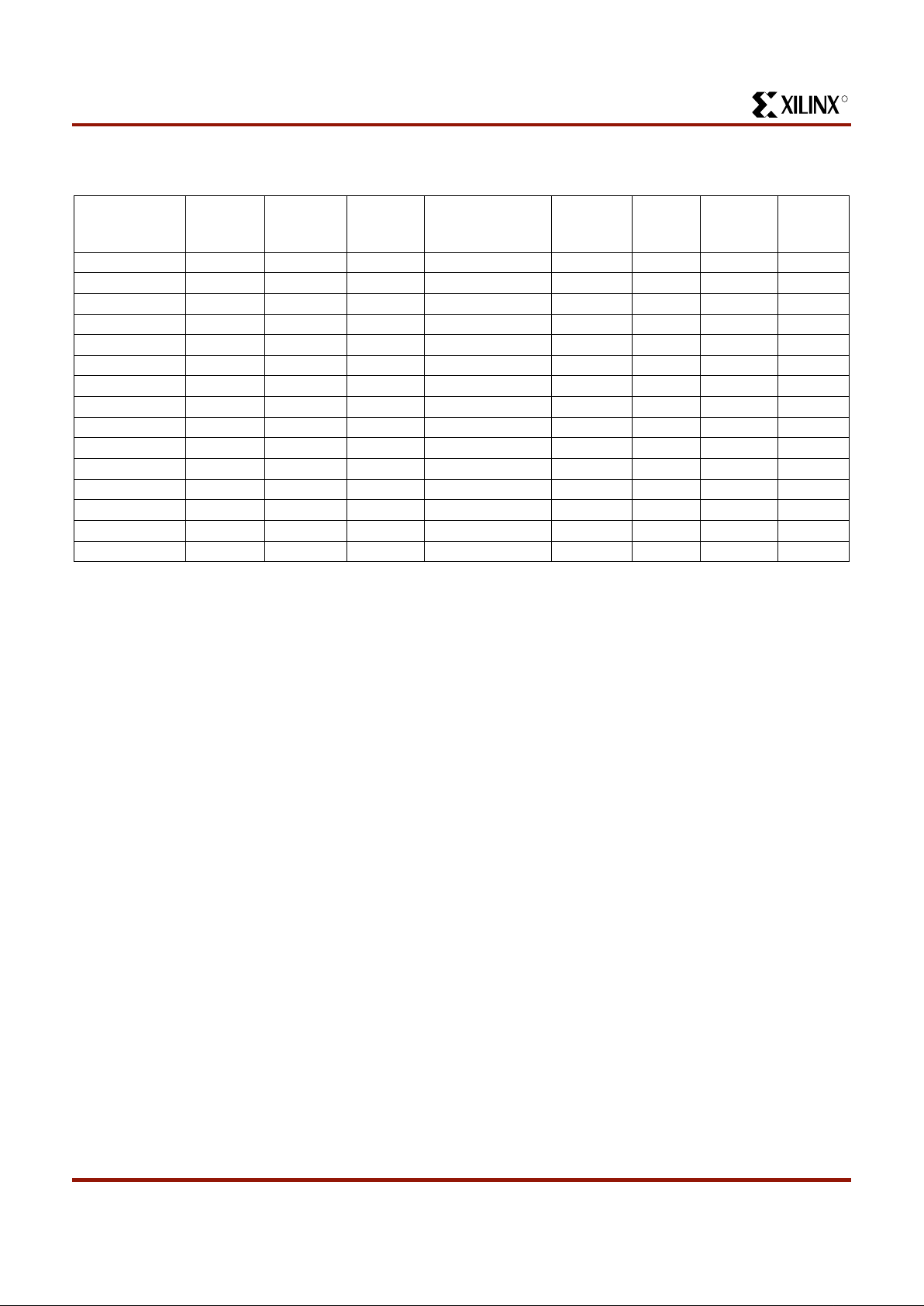
* Max values of Typical Gate Range include 20-30% of CLBs used as RAM.
Note:
All functionality in low-voltage families is the same as
in the corresponding 5-Volt family, except where numerical
references are made to timing or power.
Description
XC4000 Series devices are implemented with a regular,
flexible, programmable architecture of Configurable Logic
Blocks (CLBs), interconnected by a powerful hierarchy of
versatile routing resources, and surrounded by a perimeter
of programmable Input/Output Blocks (IOBs). They have
generous routing resources to accommodate the most
complex interconnect patterns.
The devices are customized by loading configuration data
into internal memory cells. The FPGA can either actively
read its configuration data from an external serial or
byte-parallel PROM (master modes), or the configuration
data can be written into the FPGA from an external device
(slave and peripheral modes).
XC4000 Series FPGAs are supported by powerful and
sophisticated software, covering every aspect of design
from schematic or behavioral entry, floor planning, simulation, automatic block placement and routing of interconnects, to the creation, downloading, and readback of the
configuration bit stream.
Because Xilinx FPGAs can be reprogrammed an unlimited
number of times, they can be used in innovative designs
where hardware is changed dynamically, or where hardware must be adapted to different user applications.
FPGAs are ideal for shortening design and development
cycles, and also offer a cost-effective solution for production rates well beyond 5,000 systems per month. For lowest
high-volume unit cost, a design can first be implemented in
the XC4000E or XC4000X, then migrated to one of Xilinx’
compatible HardWire mask-programmed devices.
Taking Advantage of Re-configuration
FPGA devices can be re-configured to change logic function while resident in the system. This capability gives the
system designer a new degree of freedom not available
with any other type of logic.
Hardware can be changed as easily as software. Design
updates or modifications are easy, and can be made to
products already in the field. An FPGA caneven be re-configured dynamically to perform different functions at different times.
Re-configurable logic can be used to implement system
self-diagnostics, create systems capable of being re-configured for different environments or operations, or implement multi-purpose hardwarefora given application. As an
added benefit, using re-configurable FPGA devices simplifies hardware design and debugging and shortens product
time-to-market.
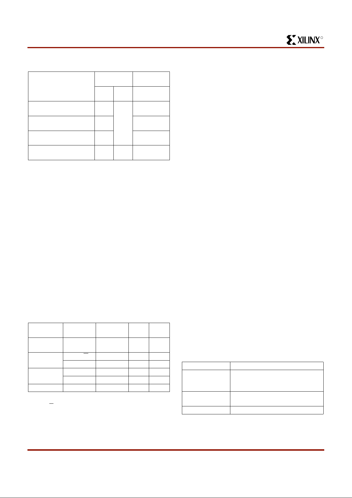
Table 1: XC4000E and XC4000X Series Field Programmable Gate Arrays
Device
Logic
Cells
Max Logic
Gates
(No RAM)
Max. RAM
Bits
(No Logic)
Typical
Gate Range
(Logic and RAM)*
CLB
Matrix
Total
CLBs
Number
of
Flip-Flops
Max.
User I/O
XC4002XL 152 1,600 2,048 1,000 - 3,000 8 x 8 64 256 64
XC4003E 238 3,000 3,200 2,000 - 5,000 10 x 10 100 360 80
XC4005E/XL 466 5,000 6,272 3,000 - 9,000 14 x 14 196 616 112
XC4006E 608 6,000 8,192 4,000 - 12,000 16 x 16 256 768 128
XC4008E 770 8,000 10,368 6,000 - 15,000 18 x 18 324 936 144
XC4010E/XL 950 10,000 12,800 7,000 - 20,000 20 x 20 400 1,120 160
XC4013E/XL 1368 13,000 18,432 10,000 - 30,000 24 x 24 576 1,536 192
XC4020E/XL 1862 20,000 25,088 13,000 - 40,000 28 x 28 784 2,016 224
XC4025E 2432 25,000 32,768 15,000 - 45,000 32 x 32 1,024 2,560 256
XC4028EX/XL 2432 28,000 32,768 18,000 - 50,000 32 x 32 1,024 2,560 256
XC4036EX/XL 3078 36,000 41,472 22,000 - 65,000 36 x 36 1,296 3,168 288
XC4044XL 3800 44,000 51,200 27,000 - 80,000 40 x 40 1,600 3,840 320
XC4052XL 4598 52,000 61,952 33,000 - 100,000 44 x 44 1,936 4,576 352
XC4062XL 5472 62,000 73,728 40,000 - 130,000 48 x 48 2,304 5,376 384
XC4085XL 7448 85,000 100,352 55,000 - 180,000 56 x 56 3,136 7,168 448
R
May 14, 1999 (Version 1.6) 6-7
XC4000E and XC4000X Series Field Programmable Gate Arrays
6
XC4000E and XC4000X Series
Compared to the XC4000
For readers already familiar with the XC4000 family of Xilinx Field Programmable Gate Arrays, the major new features in the XC4000 Series devices are listed in this
section. The biggest advantages of XC4000E and
XC4000X devices are significantly increased system
speed, greater capacity, and new architectural features,
particularly Select-RAM memory. The XC4000X devices
also offer many new routing features, including special
high-speed clock buffers that can be used to capture input
data with minimal delay.
Any XC4000E device is pinout- and bitstream-compatible
with the corresponding XC4000 device. An existing
XC4000 bitstream can be used to program an XC4000E
device. However, since the XC4000E includes many new
features, an XC4000E bitstream cannot be loaded into an
XC4000 device.
XC4000X Series devices are not bitstream-compatible with
equivalent array size devices in the XC4000 or XC4000E
families. However, equivalent array size devices, such as
the XC4025, XC4025E, XC4028EX, and XC4028XL, are
pinout-compatible.
Improvements in XC4000E and XC4000X
Increased System Speed
XC4000E and XC4000X devices can run at synchronous
system clock rates of up to 80 MHz, and internal performance can exceed 150 MHz.This increase in performance
overthepreviousfamilies stems from improvements in both
device processing and system architecture. XC4000
Series devices use a sub-micron multi-layer metal process.
In addition, many architectural improvements have been
made, as described below.
The XC4000XL family is a high performance 3.3V family
based on 0.35µ SRAM technology and supports system
speeds to 80 MHz.
PCI Compliance
XC4000 Series -2 and faster speed grades are fully PCI
compliant. XC4000E and XC4000Xdevicescan be used to
implement a one-chip PCI solution.
Carry Logic
The speed of the carry logic chain has increased dramatically. Some parameters, such as the delay on the carry
chain through a single CLB (TBYP), have improved by as
much as 50% from XC4000 values. See “Fast Carry Logic”
on page 18 for more information.
Select-RAM Memory: Edge-Triggered, Synchronous RAM Modes
The RAM in any CLB can be configured for synchronous,
edge-triggered, write operation. The read operation is not
affected by this change to an edge-triggered write.
Dual-Port RAM
A separate option converts the 16x2 RAM in any CLB into a
16x1 dual-port RAM with simultaneous Read/Write.
The function generators in each CLB can be configured as
either level-sensitive (asynchronous) single-port RAM,
edge-triggered (synchronous) single-port RAM, edge-triggered (synchronous) dual-port RAM, or as combinatorial
logic.
Configurable RAM Content
The RAM content can now be loaded at configuration time,
so that the RAM starts up with user-defined data.
H Function Generator
In current XC4000 Series devices,the H function generator
is more versatile than in the original XC4000. Its inputs can
come not only from the F and G function generators but
also from up to three of the four control input lines. The H
function generator can thus be totally or partially independent of the other two function generators, increasing the
maximum capacity of the device.
IOB Clock Enable
The two flip-flops in each IOB havea common clock enable
input, which through configuration can be activated individually for the input or output flip-flop or both. This clock
enable operates exactly like the EC pin on the XC4000
CLB. This new feature makes the IOBs more versatile, and
avoids the need for clock gating.
Output Drivers
The output pull-up structure defaults to a TTL-like
totem-pole. This driver is an n-channel pull-up transistor,
pulling to a voltage one transistor threshold below Vcc, just
like the XC4000 family outputs. Alternatively, XC4000
Series devices can be globally configured with CMOS outputs, with p-channel pull-up transistors pulling to Vcc. Also,
the configurable pull-up resistor in the XC4000 Series is a
p-channel transistor that pulls to Vcc, whereas in the original XC4000 family it is an n-channel transistor that pulls to
a voltage one transistor threshold below Vcc.

R
XC4000E and XC4000X Series Field Programmable Gate Arrays
6-8 May 14, 1999 (Version 1.6)
Input Thresholds
The input thresholds of 5V devices can be globally configured for either TTL (1.2 V threshold) or CMOS (2.5 V
threshold), just like XC2000 and XC3000 inputs. The two
global adjustments of input threshold and output level are
independent of each other. The XC4000XL family has an
input threshold of 1.6V, compatible with both 3.3V CMOS
and TTL levels.
Global Signal Access to Logic
There is additional access from global clocks to the F and
G function generator inputs.
Configuration Pin Pull-Up Resistors
During configuration, these pins have weak pull-up resistors. For the most popular configuration mode, Slave
Serial, the mode pins can thus be left unconnected. The
three mode inputs can be individually configured with or
without weak pull-up or pull-down resistors. A pull-down
resistor value of 4.7 kΩ is recommended.
The three mode inputs can be individually configured with
or without weak pull-up or pull-down resistors after configuration.
The PROGRAM input pin has a permanent weak pull-up.
Soft Start-up
Like the XC3000A, XC4000 Series devices have “Soft
Start-up.” When the configuration process is finished and
the device starts up, the first activation of the outputs is
automatically slew-rate limited. This feature avoids potential ground bounce when all outputs are turned on simultaneously. Immediately after start-up, the slew rate of the
individual outputs is, as in the XC4000 family, determined
by the individual configuration option.
XC4000 and XC4000A Compatibility
Existing XC4000 bitstreams can be used to configure an
XC4000E device.XC4000A bitstreams must be recompiled
for use with the XC4000E due to improved routing
resources, although the devices are pin-for-pincompatible.
Additional Improvements in XC4000X Only
Increased Routing
New interconnect in the XC4000X includes twenty-two
additional vertical lines in each column of CLBs and twelve
newhorizontallines in each rowofCLBs.Thetwelve“Quad
Lines” in each CLB row and column include optional repowering buffers for maximum speed. Additional high-performance routing near the IOBs enhances pin flexibility.
Faster Input and Output
A fast,dedicatedearly clocksourcedbyglobalclockbuffers
is availablefor the IOBs. To ensure synchronization with the
regular global clocks, a Fast Capture latch driven by the
early clock is available. The input data can be initially
loaded into the Fast Capture latch withthe early clock, then
transferred to the input flip-flop or latch with the low-skew
global clock. A programmable delay on the input can be
used to avoid hold-time requirements. See “IOB Input Sig-
nals” on page 20 for more information.
Latch Capability in CLBs
Storage elements in the XC4000X CLB can be configured
as either flip-flops or latches. This capability makes the
FPGA highly synthesis-compatible.
IOB Output MUX From Output Clock
A multiplexer in the IOB allows the output clock to select
either the output data or the IOB clockenableas the output
to the pad. Thus,twodifferentdata signals can share a single output pad, effectively doubling the number of device
outputs without requiring a larger, more expensive package. This multiplexer can also be configured as an
AND-gate to implement a very fast pin-to-pin path. See
“IOB Output Signals” on page 23 for more information.
Additional Address Bits
Larger devices require more bits of configuration data. A
daisy chain of several large XC4000X devices may require
a PROM that cannot be addressed by the eighteen address
bits supported in the XC4000E. The XC4000X Series
therefore extends the addressing in Master Parallel configuration mode to 22 bits.

R
May 14, 1999 (Version 1.6) 6-9
XC4000E and XC4000X Series Field Programmable Gate Arrays
6
Detailed Functional Description
XC4000 Series devices achieve high speed through
advanced semiconductor technology and improved architecture. The XC4000E and XC4000X support system clock
rates of up to 80 MHz and internal performance in excess
of 150 MHz. Compared to older Xilinx FPGA families,
XC4000 Series devices are more powerful. They offer
on-chip edge-triggered and dual-port RAM, clock enables
on I/O flip-flops, and wide-input decoders. They are more
versatile in many applications, especially those involving
RAM. Design cycles are faster due to a combination of
increased routing resources and more sophisticated software.
Basic Building Blocks
Xilinx user-programmable gate arrays include two major
configurable elements: configurable logic blocks (CLBs)
and input/output blocks (IOBs).
• CLBs provide the functional elements for constructing
the user’s logic.
• IOBs provide the interface between the package pins
and internal signal lines.
Three other types of circuits are also available:
• 3-State buffers (TBUFs) driving horizontal longlines are
associated with each CLB.
• Wide edge decoders are availablearoundthe periphery
of each device.
• An on-chip oscillator is provided.
Programmable interconnect resources provide routing
paths to connect the inputs and outputs of these configurable elements to the appropriate networks.
The functionality of each circuit block is customized during
configuration by programming internal static memory cells.
The values stored in these memory cells determine the
logic functions and interconnections implemented in the
FPGA. Each of these available circuits is described in this
section.
Configurable Logic Blocks (CLBs)
Configurable Logic Blocks implement most of the logic in
an FPGA. The principal CLB elements are shown in
Figure 1. Two 4-input function generators (F and G) offer
unrestricted versatility. Most combinatorial logic functions
need four or fewer inputs. However, a third function generator (H) is provided. The H function generator has three
inputs. Either zero, one, or two of these inputs can be the
outputs of F and G; the other input(s) are from outside the
CLB. The CLB can, therefore, implement certain functions
of up to nine variables, like parity check or expandable-identity comparison of two sets of four inputs.
Each CLB contains two storage elements that can be used
to store the function generator outputs. However, the storage elements and function generators can also be used
independently. These storage elements can be configured
as flip-flops in both XC4000E and XC4000X devices; in the
XC4000X they can optionally be configured as latches. DIN
can be used as a direct input to either of the two storage
elements. H1 can drive the other through the H function
generator. Function generator outputs can also drive two
outputs independent of the storage element outputs. This
versatility increases logic capacity and simplifies routing.
Thirteen CLB inputs and four CLB outputs provide access
to the function generators and storage elements. These
inputs and outputs connect to the programmable interconnect resources outside the block.
Function Generators
Four independent inputs are provided to each of two function generators (F1 - F4 and G1 - G4). These function generators, with outputs labeled F’ and G’, are each capableof
implementing any arbitrarily defined Boolean function of
four inputs. The function generators are implemented as
memory look-up tables. The propagation delay is therefore
independent of the function implemented.
A third function generator, labeled H’, can implement any
Boolean function of its three inputs. Two of these inputs can
optionally be the F’ and G’ functional generator outputs.
Alternatively, one or both of these inputs can come from
outside the CLB (H2, H0). The third input must come from
outside the block (H1).
Signals from the function generators can exit the CLB on
two outputs.F’orH’canbeconnectedtotheXoutput.G’or
H’ can be connected to the Y output.
A CLB can be used to implement any of the following functions:
• any function of up to four variables, plus any second
function of up to four unrelated variables, plus any third
function of up to three unrelated variables
1
• any single function of five variables
• any function of four variables together with some
functions of six variables
• some functions of up to nine variables.
Implementing wide functions in a single block reduces both
the number of blocks required and the delay in the signal
path, achieving both increased capacity and speed.
The versatility of the CLB function generators significantly
improves system speed. In addition, the design-software
tools can deal with each function generator independently.
This flexibility improves cell usage.
1. When three separate functions are generated, one of the function outputs must be captured in a flip-flop internal to the CLB. Only two
unregistered function generator outputs are available from the CLB.
R
XC4000E and XC4000X Series Field Programmable Gate Arrays
6-10 May 14, 1999 (Version 1.6)
Flip-Flops
The CLB can pass the combinatorial output(s) to the interconnect network, but can also store the combinatorial
results or other incoming data in one or two flip-flops, and
connect their outputs to the interconnect network as well.
The two edge-triggered D-type flip-flops have common
clock (K) and clock enable (EC) inputs. Either or both clock
inputs can also be permanently enabled. Storage element
functionality is described in Table 2.
Latches (XC4000X only)
The CLB storage elements can also be configured as
latches. The two latches have common clock (K) and clock
enable (EC) inputs. Storage element functionality is
described in Table 2.
Clock Input
Each flip-flop can be triggered on either the rising or falling
clock edge. The clock pin is shared by both storage elements. However, the clock is individually invertible for each
storage element. Any inverter placed on the clock input is
automatically absorbed into the CLB.
Clock Enable
The clock enable signal (EC) is active High. The EC pin is
shared by both storage elements. If left unconnected for
either, the clock enable for that storage element defaults to
the active state. EC is not invertible within the CLB.
LOGIC
FUNCTION
OF
G1-G4
G
4
G
3
G
2
G
1
G'
LOGIC
FUNCTION
OF
F1-F4
F
4
F
3
F
2
F
1
F'
LOGIC
FUNCTION
OF
F', G',
AND
H1
H'
DIN
F'
G'
H'
DIN
F'
G'
H'
G'
H'
H'
F'
S/R
CONTROL
D
EC
RD
Bypass
Bypass
SD
YQ
XQ
Q
S/R
CONTROL
D
EC
RD
SD
Q
1
1
K
(CLOCK)
Multiplexer Controlled
by Configuration Program
Y
X
DIN/H
2
H
1
SR/H
0
EC
X6692
C1 • • • C4
4
Figure 1: Simplified Block Diagram of XC4000 Series CLB (RAM and Carry Logic functions not shown)
Table 2: CLB Storage Element Functionality
(active rising edge is shown)
Mode K EC SR D Q
Power-Up or
GSR
XXXXSR
Flip-Flop
XX1XSR
__/ 1* 0* D D
0X0*XQ
Latch
11*0*XQ
01*0*DD
Both X 0 0* X Q
Legend:
X
__/
SR
0*
1*
Don’t care
Rising edge
Set or Reset value. Reset is default.
Input is Low or unconnected (default value)
Input is High or unconnected (default value)

R
May 14, 1999 (Version 1.6) 6-11
XC4000E and XC4000X Series Field Programmable Gate Arrays
6
Set/Reset
An asynchronous storage element input (SR) can be configured as either set or reset. This configuration option
determines the state in which each flip-flop becomes operational after configuration. It also determines the effectof a
Global Set/Reset pulse during normal operation, and the
effect of a pulse on the SR pin of the CLB. All three
set/reset functions for any single flip-flop are controlled by
the same configuration data bit.
The set/reset state can be independently specified for each
flip-flop. This input can also be independently disabled for
either flip-flop.
The set/reset state is specified by using the INIT attribute,
or by placing the appropriate set or reset flip-flop library
symbol.
SR is active High. It is not invertible within the CLB.
Global Set/Reset
A separate Global Set/Reset line (not shown in Figure 1)
sets or clears each storage element during power-up,
re-configuration, or when a dedicated Reset net is driven
active. This global net (GSR) does not compete with other
routing resources; it uses a dedicated distribution network.
Each flip-flop is configured as either globally set or reset in
the same way that the local set/reset (SR) is specified.
Therefore, if a flip-flop is set by SR, it is also set by GSR.
Similarly, a reset flip-flop is reset by both SR and GSR.
GSR can be driven from any user-programmable pin as a
global reset input. To use this globalnet, place an input pad
and input buffer in the schematic or HDL code, driving the
GSR pin of the STARTUP symbol. (See Figure 2.) A specific pin location can be assigned to this input using a LOC
attribute or property, just as with any other user-programmable pad. An inverter can optionally be inserted after the
input buffer to invert the sense of the Global Set/Reset signal.
Alternatively, GSR can be driven from any internal node.
Data Inputs and Outputs
The source of a storage element data input is programmable. It is driven by any of the functions F’, G’, and H’, or by
the Direct In (DIN) blockinput.Theflip-flopsorlatchesdrive
the XQ and YQ CLB outputs.
Two fast feed-through paths are available, as shown in
Figure 1. A two-to-one multiplexer on each of the XQ and
YQ outputs selects between a storage element output and
any of the control inputs. This bypass is sometimes used by
the automated router to repower internal signals.
Control Signals
MultiplexersintheCLBmapthefourcontrolinputs(C1- C4
in Figure 1) into the four internal control signals (H1,
DIN/H2, SR/H0, and EC). Any of theseinputscan drive any
of the four internal control signals.
When the logic function is enabled, the four inputs are:
• EC — Enable Clock
• SR/H0 — Asynchronous Set/Reset or H function
generator Input 0
• DIN/H2 — Direct In or H function generator Input 2
• H1 — H function generator Input 1.
When the memory function is enabled, the four inputs are:
• EC — Enable Clock
• WE — Write Enable
• D0 — Data Input to F and/or G function generator
• D1 — Data input to G function generator (16x1 and
16x2 modes) or 5th Address bit (32x1 mode).
Using FPGA Flip-Flops and Latches
The abundance of flip-flops in the XC4000 Series invites
pipelined designs. This is a powerful way of increasing performance by breaking the function into smaller subfunctions and executing them in parallel, passing on the results
through pipeline flip-flops. This method should be seriously
considered wherever throughput is more important than
latency.
To include a CLB flip-flop, place the appropriate library
symbol. For example, FDCE is a D-type flip-flop with clock
enable and asynchronous clear. The corresponding latch
symbol (for the XC4000X only) is called LDCE.
In XC4000 Series devices,theflipflopscanbeusedasregisters or shift registers without blocking the function generators from performing a different, perhaps unrelated task.
This abilityincreasesthefunctionalcapacityofthedevices.
The CLB setup time is specified between the function generator inputs and the clockinput K. Therefore, the specified
CLB flip-flop setup time includes the delay through the
function generator.
Using Function Generators as RAM
Optional modes for each CLB make the memory look-up
tables in the F’ and G’ function generators usable as an
array of Read/Write memory cells. Available modes are
level-sensitive (similar to the XC4000/A/H families),
edge-triggered, and dual-port edge-triggered. Depending
on the selected mode, a single CLB can be configured as
either a 16x2, 32x1, or 16x1 bit array.
PAD
IBUF
GSR
GTS
CLK
DONEIN
Q1Q4
Q2
Q3
STARTUP
X5260
Figure 2: Schematic Symbols for Global Set/Reset
R
XC4000E and XC4000X Series Field Programmable Gate Arrays
6-12 May 14, 1999 (Version 1.6)
Supported CLB memory configurations and timing modes
for single- and dual-port modes are shown in Table 3.
XC4000 Series devices are the first programmable logic
devices with edge-triggered (synchronous) and dual-port
RAM accessible to the user. Edge-triggered RAM simplifies system timing. Dual-port RAM doubles the effective
throughput of FIFO applications. These features can be
individually programmed in any XC4000 Series CLB.
Advantages of On-Chip and Edge-Triggered RAM
The on-chip RAM is extremely fast.Thereadaccess time is
the same as the logic delay. The write access time is
slightly slower. Both access times are much faster than
any off-chip solution, because they avoid I/O delays.
Edge-triggered RAM, also called synchronous RAM, is a
feature never before available in a Field Programmable
Gate Array. The simplicity of designing with edge-triggered
RAM, and the markedly higher achievable performance,
add up to a significant improvement over existing devices
with on-chip RAM.
Three application notes are available from Xilinx that discuss edge-triggered RAM: “
XC4000E Edge-Triggered and
Dual-Port RAM Capability,
”“
Implementing FIFOs in
XC4000E RAM,
” and “
Synchronous and Asynchronous
FIFO Designs
.” All three application notes apply to both
XC4000E and XC4000X RAM.
RAM Configuration Options
The function generators in any CLB can be configured as
RAM arrays in the following sizes:
• Two 16x1 RAMs: two data inputs and two data outputs
with identical or, if preferred, different addressing for
each RAM
• One 32x1 RAM: one data input and one data output.
One F or Gfunction generator can be configuredas a 16x1
RAM while the other function generators are used to implement any function of up to 5 inputs.
Additionally, the XC4000 Series RAM may have either of
two timing modes:
• Edge-Triggered (Synchronous): data written by the
designated edge of the CLB clock. WE acts as a true
clock enable.
• Level-Sensitive (Asynchronous): an external WE signal
acts as the write strobe.
The selected timing mode applies to both function generators within a CLB when both are configured as RAM.
The number of read ports is also programmable:
• Single Port: each function generator has a common
read and write port
• Dual Port: both function generators are configured
together as a single 16x1 dual-port RAM with one write
port and two read ports. Simultaneous read and write
operations to the same or different addresses are
supported.
RAM configuration options are selected by placing the
appropriate library symbol.
Choosing a RAM Configuration Mode
The appropriate choice of RAM mode for a given design
should be based on timing and resource requirements,
desired functionality, and the simplicity of the design process. Recommended usage is shown in Table 4.
The difference between level-sensitive, edge-triggered,
and dual-port RAM is only in the write operation. Read
operation and timing is identical for all modes of operation.
RAM Inputs and Outputs
The F1-F4 and G1-G4 inputs to the function generators act
as address lines, selecting a particular memory cell in each
look-up table.
The functionality of the CLB control signals changes when
the function generators are configured as RAM. The
DIN/H2, H1, and SR/H0 lines become the two data inputs
(D0, D1) and the Write Enable (WE) input for the 16x2
memory. When the 32x1 configuration is selected, D1 acts
as the fifth address bit and D0 is the data input.
The contents of the memory cell(s) being addressed are
available at the F’ and G’ function-generator outputs. They
can exittheCLBthroughitsXandYoutputs,orcan be captured in the CLB flip-flop(s).
Configuring the CLB function generators as Read/Write
memory does not affect the functionality of the other por-
Table 3: Supported RAM Modes
16
x
1
16
x
2
32
x
1
Edge-
Triggered
Timing
Level-
Sensitive
Timing
Single-Port √√√ √ √
Dual-Port √
√
Table 4: RAM Mode Selection
Level-Sens
itive
Edge-Trigg
ered
Dual-Port
Edge-Trigg
ered
Use for New
Designs?
No Yes Yes
Size (16x1,
Registered)
1/2 CLB 1/2 CLB 1 CLB
Simultaneous
Read/Write
No No Yes
Relative
Performance
X2X
2X (4X
effective)
R
May 14, 1999 (Version 1.6) 6-13
XC4000E and XC4000X Series Field Programmable Gate Arrays
6
tions of the CLB, with the exception of the redefinition of the
control signals. In 16x2 and 16x1 modes, the H’ function
generator can be used to implement Boolean functions of
F’, G’, and D1, and the D flip-flops can latch theF’,G’,H’,or
D0 signals.
Single-Port Edge-Triggered Mode
Edge-triggered (synchronous) RAM simplifies timing
requirements. XC4000 Series edge-triggered RAM timing
operates like writing to a data register. Data and address
are presented. The register is enabled for writing by a logic
High on the write enable input, WE. Then a rising or falling
clock edge loads the data into the register, as shown in
Figure 3.
Complex timing relationships between address, data, and
write enable signals are not required, and theexternalwrite
enable pulse becomes a simple clock enable. The active
edge of WCLK latches the address, input data, and WE sig-
nals. An internal write pulse is generated that performs the
write. See Figure 4 and Figure 5 for block diagrams of a
CLB configured as 16x2 and 32x1 edge-triggered, single-port RAM.
The relationships between CLB pins and RAM inputs and
outputs for single-port, edge-triggered mode are shown in
Table 5.
The Write Clock input (WCLK) can be configured as active
on either the rising edge (default) or the falling edge. It uses
the same CLB pin (K) used to clock the CLB flip-flops,butit
can be independently inverted. Consequently, the RAM
output can optionally be registered within the same CLB
either by the same clock edge as the RAM, or by the opposite edge of this clock. The sense of WCLK applies to both
function generators in the CLB when both are configured
as RAM.
The WE pin is active-High and is not invertible within the
CLB.
Note: The pulse following the active edge of WCLK (T
WPS
in Figure 3) must be less than one millisecond wide. For
most applications, this requirement is not overly restrictive;
however, it must not be forgotten. Stopping WCLK at this
point in the write cyclecould result in excessivecurrent and
even damage to the larger devices if many CLBs are configured as edge-triggered RAM.
X6461
WCLK (K)
WE
ADDRESS
DATA IN
DATA OUT OLD NEW
T
DSS
T
DHS
T
ASS
T
AHS
T
WSS
T
WPS
T
WHS
T
WOS
T
ILO
T
ILO
Figure 3: Edge-Triggered RAM Write Timing
Table 5: Single-Port Edge-Triggered RAM Signals
RAM Signal CLB Pin Function
D D0 or D1 (16x2,
16x1), D0 (32x1)
Data In
A[3:0] F1-F4 or G1-G4 Address
A[4] D1 (32x1) Address
WE WE Write Enable
WCLK K Clock
SPO
(Data Out)
F’ or G’ Single Port Out
(Data Out)
R
XC4000E and XC4000X Series Field Programmable Gate Arrays
6-14 May 14, 1999 (Version 1.6)
G'
4
G1 • • • G4
F1 • • • F4
C1 • • • C4
WRITE
DECODER
1 of 16
D
IN
16-LATCH
ARRAY
X6752
4
4
MUX
F'
WRITE
DECODER
1 of 16
D
IN
16-LATCH
ARRAY
READ
ADDRESS
READ
ADDRESS
WRITE PULSE
LATCH
ENABLE
LATCH
ENABLE
K
(CLOCK)
WE
D
1
D
0
EC
WRITE PULSE
MUX
4
4
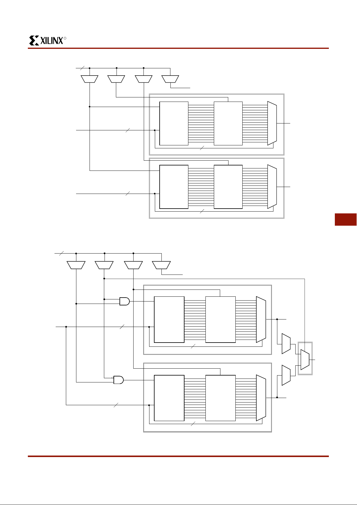
Figure 4: 16x2 (or 16x1) Edge-Triggered Single-Port RAM
G'
4
G1 • • • G4
F1 • • • F4
C1 • • • C4
WRITE
DECODER
1 of 16
D
IN
16-LATCH
ARRAY
X6754
4
4
MUX
F'
WRITE
DECODER
1 of 16
D
IN
16-LATCH
ARRAY
READ
ADDRESS
READ
ADDRESS
WRITE PULSE
LATCH
ENABLE
LATCH
ENABLE
K
(CLOCK)
WE
D1/A
4
D
0
EC
EC
WRITE PULSE
MUX
4
4
H'
Figure 5: 32x1 Edge-Triggered Single-Port RAM (F and G addresses are identical)
R
May 14, 1999 (Version 1.6) 6-15
XC4000E and XC4000X Series Field Programmable Gate Arrays
6
Dual-Port Edge-Triggered Mode
In dual-port mode, both the F and G function generators
are used to create a single 16x1 RAM array with one write
port and two read ports. The resulting RAM array can be
read and written simultaneously at two independent
addresses. Simultaneous read and write operations at the
same address are also supported.
Dual-port mode always has edge-triggered write timing, as
shown in Figure 3.
Figure 6 shows a simple model of an XC4000 Series CLB
configured as dual-port RAM. One address port, labeled
A[3:0], supplies both the read and write address for the F
function generator. This function generator behaves the
same as a 16x1 single-port edge-triggered RAM array. The
RAM output, Single Port Out (SPO), appears at the F function generator output. SPO, therefore, reflects the data at
address A[3:0].
The other address port, labeled DPRA[3:0] for Dual Port
Read Address, supplies the read address for the G function
generator. The write address for the G function generator,
however, comes from the address A[3:0]. The output from
this 16x1 RAM array, Dual Port Out (DPO), appears at the
G function generator output. DPO, therefore, reflects the
data at address DPRA[3:0].
Therefore, by using A[3:0] for the write address and
DPRA[3:0] for the read address, and reading only the DPO
output, a FIFO that can read and write simultaneously is
easily generated. Simultaneous access doubles the effective throughput of the FIFO.
The relationships between CLB pins and RAM inputs and
outputs for dual-port, edge-triggered mode are shown in
Table 6. See Figure 7 on page 16 for a block diagram of a
CLB configured in this mode.
Table 6: Dual-Port Edge-Triggered RAM Signals
Note: The pulse following the active edge of WCLK (T
WPS
in Figure 3) must be less than one millisecond wide. For
most applications, this requirement is not overly restrictive;
however, it must not be forgotten. Stopping WCLK at this
point in the write cyclecould result in excessivecurrent and
even damage to the larger devices if many CLBs are configured as edge-triggered RAM.
Single-Port Level-Sensitive Timing Mode
Note: Edge-triggered mode is recommended for all new
designs. Level-sensitive mode, also called asynchronous
mode, is still supported for XC4000 Series backward-compatibility with the XC4000 family.
Level-sensitive RAM timing is simple in concept but can be
complicated in execution. Data and address signals are
presented, then a positive pulse on the write enable pin
(WE) performs a write into the RAM at the designated
address. As indicated by the “level-sensitive” label, this
RAM acts likea latch. During the WE High pulse, changing
the data lines results in newdatawritten to the old address.
Changing the address lines while WE is High results in spurious data written to the new address—and possibly at
other addresses as well, as the address lines inevitably do
not all change simultaneously.
The user must generate a carefully timed WE signal. The
delayonthe WE signal and the address lines must be carefully verified to ensure that WE does not become active
until after the address lines have settled, and that WE goes
inactive before the address lines change again. The data
must be stable before and after the falling edge of WE.
In practical terms, WE isusually generated by a 2X clock. If
a 2X clock is not available, the falling edge of the system
clock can be used. However, there are inherent risks in this
approach, since the WE pulse must be guaranteed inactive
before the next rising edge of the system clock. Several
older application notes are available from Xilinx that discuss the design of level-sensitive RAMs. These application
notes include XAPP031, “
Using the XC4000 RAM Capabil-
ity
,” and XAPP042, “
High-Speed RAM Design in XC4000
.”
However, the edge-triggered RAM available in the XC4000
Series is superior to level-sensitive RAM for almost every
application.
WE
WE
DDQ
DQ
D
DPRA[3:0]
A[3:0]
AR[3:0]
AW[3:0]
WE
D
AR[3:0]
AW[3:0]
RAM16X1D Primitive
F Function Generator
G Function Generator
DPO (Dual Port Out)
Registered DPO
SPO (Single Port Out)
Registered SPO
WCLK
X6755
Figure 6: XC4000 Series Dual-Port RAM, Simple
Model
RAM Signal CLB Pin Function
D D0 Data In
A[3:0] F1-F4 Read Address for F,
Write Address for F and G
DPRA[3:0] G1-G4 Read Address for G
WE WE Write Enable
WCLK K Clock
SPO F’ Single Port Out
(addressed by A[3:0])
DPO G’ Dual Port Out
(addressed by DPRA[3:0])
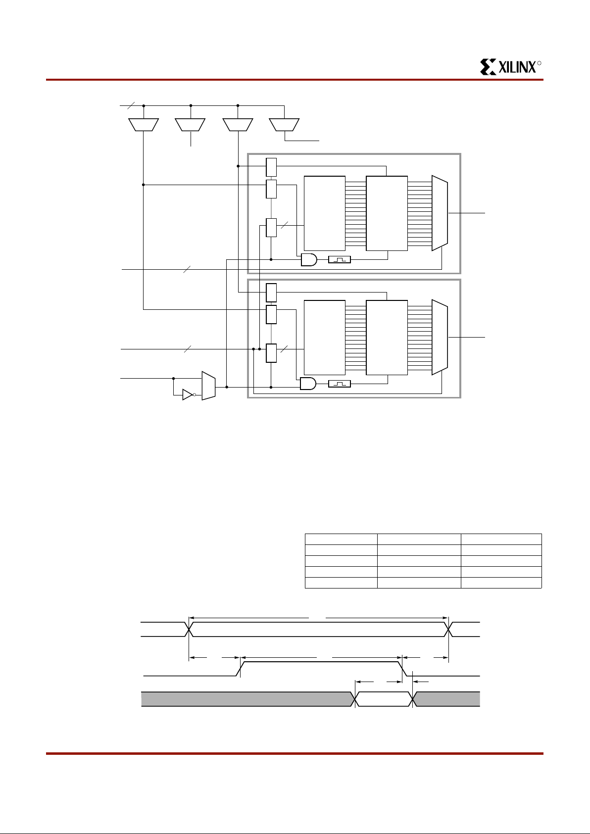
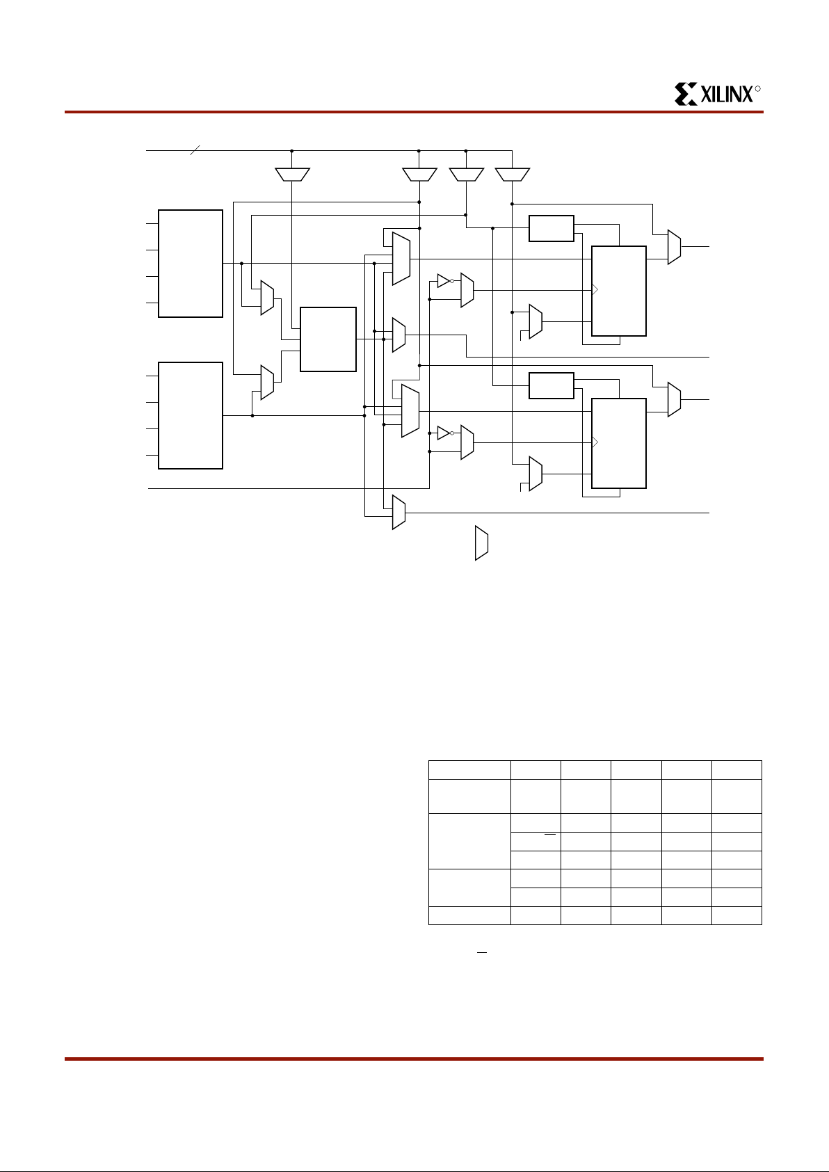
R
XC4000E and XC4000X Series Field Programmable Gate Arrays
6-16 May 14, 1999 (Version 1.6)
Figure 8 shows the write timing for level-sensitive, sin-
gle-port RAM.
The relationships between CLB pins and RAM inputs and
outputs for single-port level-sensitive mode are shown in
Table 7.
Figure 9 and Figure 10 show blockdiagrams of a CLB con-
figured as 16x2 and 32x1 level-sensitive, single-port RAM.
Initializing RAM at Configuration
Both RAM and ROM implementations of the XC4000
Series devices are initialized during configuration. The initial contents are defined via an INIT attribute or property
attached to the RAM or ROM symbol, as described in the
schematic library guide. If not defined, all RAM contents
are initialized to all zeros, by default.
RAM initialization occurs only during configuration. The
RAM content is not affected by Global Set/Reset.
Table 7: Single-Port Level-Sensitive RAM Signals
G'
G1 • • • G4
F1 • • • F4
WRITE
DECODER
1 of 16
D
IN
16-LATCH
ARRAY
X6748
4
4
MUX
F'
WRITE
DECODER
1 of 16
D
IN
16-LATCH
ARRAY
READ
ADDRESS
READ
ADDRESS
WRITE PULSE
LATCH
ENABLE
LATCH
ENABLE
K
(CLOCK)
WRITE PULSE
MUX
4
4
C1 • • • C4
4
WE
D
1
D
0
EC
Figure 7: 16x1 Edge-Triggered Dual-Port RAM
RAM Signal CLB Pin Function
D D0 or D1 Data In
A[3:0] F1-F4 or G1-G4 Address
WE WE Write Enable
O F’ or G’ Data Out
WC
T
ADDRESS
WRITE ENABLE
DATA IN
AS
T
WP
T
DS
T
DH
T
REQUIRED
AH
T
X6462
Figure 8: Level-Sensitive RAM Write Timing
R
May 14, 1999 (Version 1.6) 6-17
XC4000E and XC4000X Series Field Programmable Gate Arrays
6
Enable
G'
4
G1 • • • G4
F1 • • • F4
WRITE
DECODER
1 of 16
D
IN
16-LATCH
ARRAY
X6746
4
READ ADDRESS
MUX
Enable
F'
WRITE
DECODER
1 of 16
D
IN
16-LATCH
ARRAY
4
READ ADDRESS
MUX
4
C1 • • • C4
4
WE
D
1
D
0
EC
Figure 9: 16x2 (or 16x1) Level-Sensitive Single-Port RAM
Enable
WRITE
DECODER
1 of 16
D
IN
16-LATCH
ARRAY
X6749
4
READ ADDRESS
MUX
Enable
WRITE
DECODER
1 of 16
D
IN
16-LATCH
ARRAY
4
READ ADDRESS
MUX
G'
4
G1 • • • G4
F1 • • • F4
C1 • • • C4
4
F'
WE
D1/A
4
D
0
EC
4
H'
Figure 10: 32x1 Level-Sensitive Single-Port RAM (F and G addresses are identical)
R
XC4000E and XC4000X Series Field Programmable Gate Arrays
6-18 May 14, 1999 (Version 1.6)
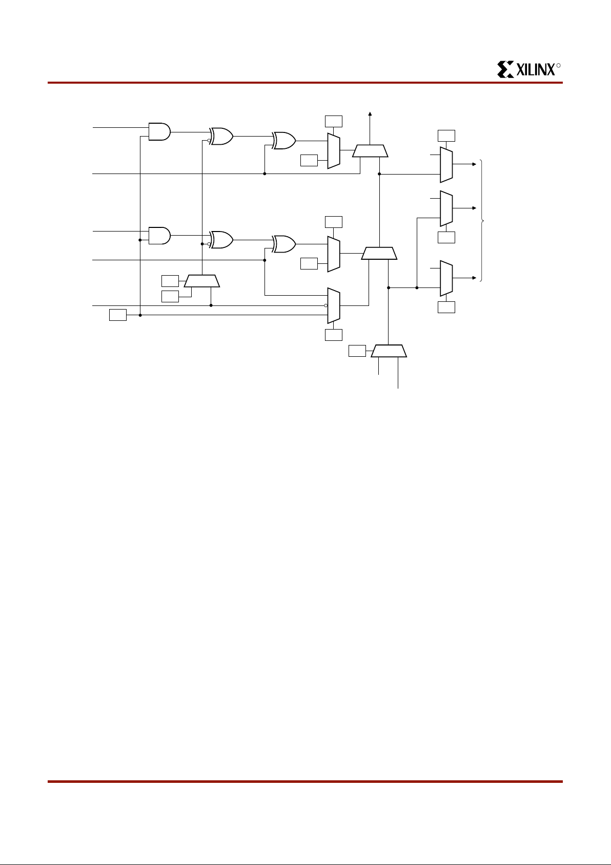
Fast Carry Logic
Each CLB F and G function generator contains dedicated
arithmetic logic for the fast generation of carry and borrow
signals. This extra output is passed on to the function generator in the adjacent CLB. The carry chain is independent
of normal routing resources.
Dedicated fast carry logic greatly increases the efficiency
and performance of adders, subtractors, accumulators,
comparators and counters. It also opens the door to many
new applications involving arithmetic operation, where the
previousgenerationsofFPGAs were not fastenough or too
inefficient. High-speed address offset calculations in microprocessor or graphics systems, and high-speed addition in
digital signal processing are two typical applications.
The two 4-input function generators can be configured as a
2-bit adder with built-in hidden carry that can be expanded
to any length. This dedicated carry circuitry is so fast and
efficient that conventional speed-up methods like carry
generate/propagate are meaningless even at the 16-bit
level, and of marginal benefit at the 32-bit level.
This fast carry logic is one of the more significant features
of the XC4000 Series, speedingup arithmetic and counting
into the 70 MHz range.
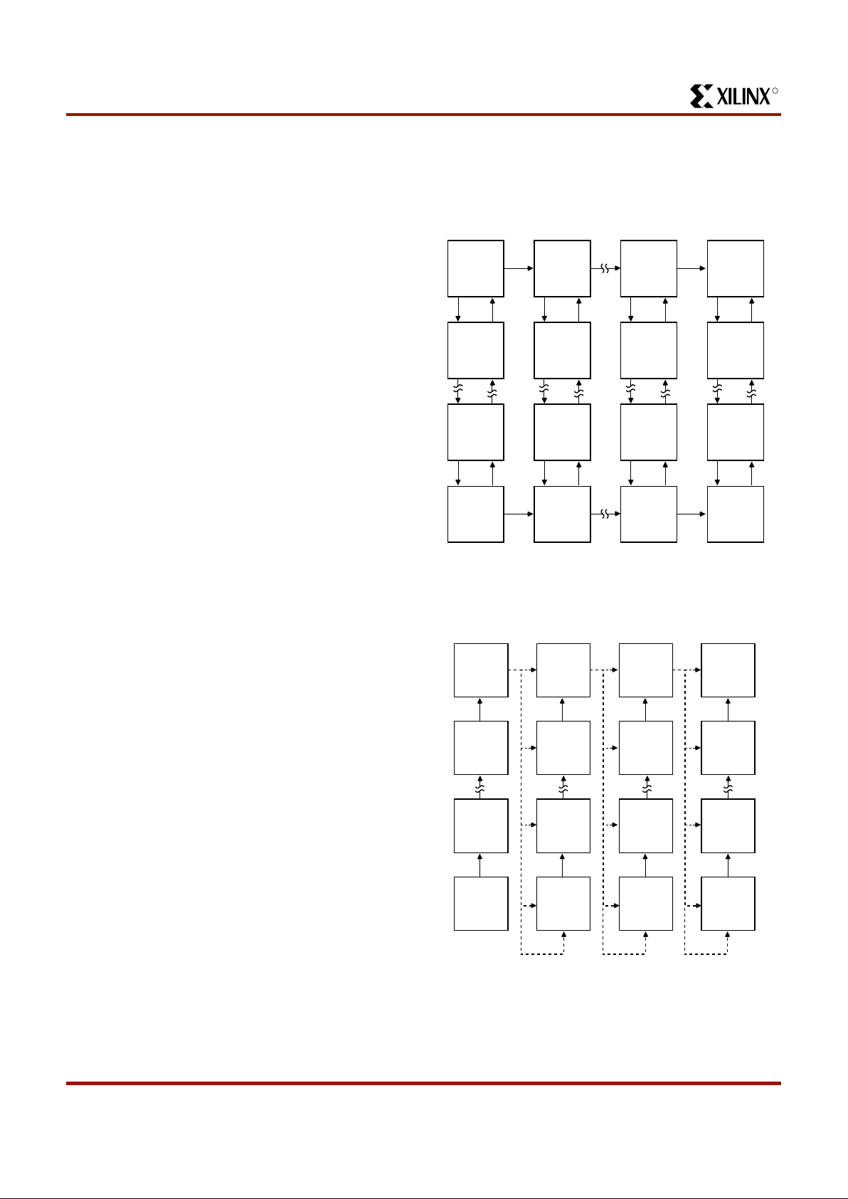
The carry chain in XC4000E devices can run either up or
down. At the top and bottom of the columns where there
are no CLBs aboveor below, the carry is propagated to the
right. (See Figure 11.) In order to improve speed in the
high-capacity XC4000X devices, which can potentially
have very long carry chains, the carry chain travels upward
only, as shown in Figure 12. Additionally,standardinterconnect can be used to route a carry signal in the downward
direction.
Figure 13 on page 19 shows an XC4000E CLB with dedi-
cated fast carry logic. The carry logic in the XC4000X is
similar, except that COUT exits at the top only, and the signal CINDOWN does not exist. As shown in Figure 13, the
carry logic shares operandandcontrol inputs with the function generators. The carry outputs connect to the function
generators, where they are combined with the operands to
form the sums.
Figure 14 on page 20 shows the details of the carry logic
for the XC4000E. This diagram shows the contents of the
box labeled “CARRY LOGIC” in Figure 13. The XC4000X
carry logic is very similar, but a multiplexer on the
pass-through carry chain has been eliminated to reduce
delay. Additionally, in the XC4000X the multiplexer on the
G4 path has a memory-programmable 0 input, which permits G4 to directly connect to COUT. G4 thus becomes an
additional high-speed initialization path for carry-in.
The dedicated carry logic is discussed in detail in Xilinx
document XAPP 013: “
Using the Dedicated Carry Logic in
XC4000
.” This discussion also applies to XC4000E
devices, and to XC4000X devices when the minor logic
changes are taken into account.
The fast carry logic can be accessed by placing special
library symbols, or by using Xilinx Relationally Placed Macros (RPMs) that already include these symbols.
X6687
CLB CLB CLB CLB
CLB CLB CLB CLB
CLB
CLB
CLB
CLB
CLB
CLB
CLB
CLB
Figure 11: Available XC4000E Carry Propagation
Paths
X6610
CLB CLB CLB CLB
CLB CLB CLB CLB
CLB
CLB
CLB
CLB
CLB
CLB
CLB
CLB
Figure 12: Available XC4000X Carry Propagation
Paths (dotted lines use general interconnect)
R
May 14, 1999 (Version 1.6) 6-19
XC4000E and XC4000X Series Field Programmable Gate Arrays
6
DQ
S/R
EC
YQ
Y
DIN
H
G
F
G
H
DQ
S/R
EC
XQ
DIN
H
G
F
H
X
H
F
G
G4
G3
G2
G1
F
F3
F2
F1
F4
F
CARRY
G
CARRY
C
C
DOWN
CARRY
LOGIC
D
CC
UP
K S/R EC
H1
X6699
OUT
IN
OUT
IN
IN
C
OUT0
Figure 13: Fast Carry Logic in XC4000E CLB (shaded area not present in XC4000X)
R
XC4000E and XC4000X Series Field Programmable Gate Arrays
6-20 May 14, 1999 (Version 1.6)
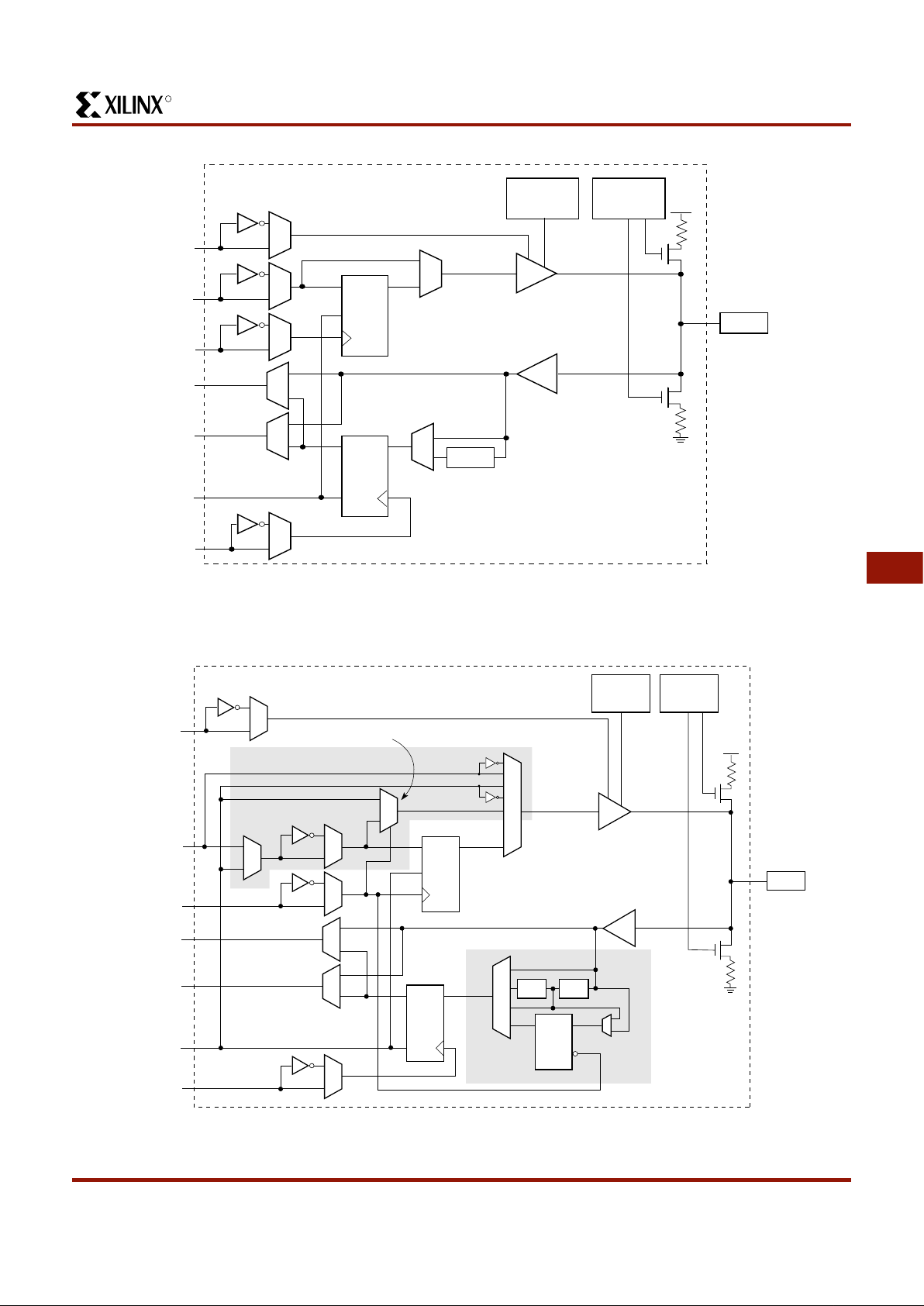
Input/Output Blocks (IOBs)
User-configurable input/output blocks (IOBs) provide the
interface between external package pins and the internal
logic. Each IOB controls one package pin and can be configured for input, output, or bidirectional signals.
Figure 15 shows a simplified block diagram of the
XC4000E IOB. A more complete diagram which includes
the boundary scan logic of the XC4000E IOB can be found
in Figure 40 on page 43, in the “Boundary Scan” section.
The XC4000X IOB contains some special features not
included in the XC4000E IOB. These features are highlighted in a simplified block diagram foundin Figure 16, and
discussed throughout this section. When XC4000X special
features are discussed, they are clearly identified in the
text. Any feature not so identified is present in both
XC4000E and XC4000X devices.
IOB Input Signals
Two paths, labeled I1 and I2 in Figure 15 and Figure 16,
bring input signals into the array. Inputs also connect to an
input register that can be programmed as either an
edge-triggered flip-flop or a level-sensitive latch.
The choice is made by placing the appropriate library symbol. For example,IFDisthe basic input flip-flop (rising edge
triggered), and ILD is the basic input latch (transparent-High). Variations with inverted clocks are available, and
some combinations of latches and flip-flops can be implemented in a single IOB, as described in the
XACT Libraries
Guide
.
The XC4000E inputs can be globally configured for either
TTL (1.2V) or 5.0 volt CMOS thresholds, using an option in
the bitstream generation software. There is a slight input
hysteresis of about 300mV. The XC4000E output levels are
also configurable; the two global adjustments of input
threshold and output level are independent.
Inputs on the XC4000XL are TTL compatible and 3.3V
CMOS compatible. Outputs on the XC4000XL are pulled to
the 3.3V positive supply.
The inputs of XC4000 Series 5-Volt devices can be driven
by the outputs of any 3.3-Volt device,if the 5-Voltinputs are
in TTL mode.
Supported sources for XC4000 Series device inputs are
shown in Table 8.
01
01
M
M
0
1
01
M
0
1
M
10
M
M
0
3
M
1
M
I
G1
G4
F2
F1
F3
C
OUT
G2
G3
F4
C
INUP
C
IN DOWN
X2000
TO
FUNCTION
GENERATORS
M
M
M
C
OUT0
Figure 14: Detail of XC4000E Dedicated Carry Logic
R
May 14, 1999 (Version 1.6) 6-21
XC4000E and XC4000X Series Field Programmable Gate Arrays
6
Q
Flip-
Flop/
Latch
D
D
CE
CE
Q
Out
T
Output
Clock
I
Input
Clock
Clock
Enable
Delay
Pad
Flip-Flop
Slew Rate
Control
Output
Buffer
Input
Buffer
Passive
Pull-Up/
Pull-Down
2
I
1
X6704
Figure 15: Simplified Block Diagram of XC4000E IOB
Q
Flip-Flop/
Latch
Fast
Capture
Latch
D
Q
Latch
D
G
D
0
1
CE
CE
Q
Out
T
Output Clock
I
Input Clock
Clock Enable
Pad
Flip-Flop
Slew Rate
Control
Output
Buffer
Output MUX
Input
Buffer
Passive
Pull-Up/
Pull-Down
2
I
1
X5984
Delay Delay
Figure 16: Simplified Block Diagram of XC4000X IOB (shaded areas indicate differences from XC4000E)
R
XC4000E and XC4000X Series Field Programmable Gate Arrays
6-22 May 14, 1999 (Version 1.6)
XC4000XL 5-Volt Tolerant I/Os
The I/Os on the XC4000XL are fully 5-volt tolerant even
though the VCCis 3.3 volts. This allows 5 V signals to
directly connect to the XC4000XL inputs without damage,
as shown in Table 8. In addition, the 3.3 volt VCCcan be
applied before or after 5 voltsignals are applied to the I/Os.
This makes the XC4000XL immune to power supply
sequencing problems.
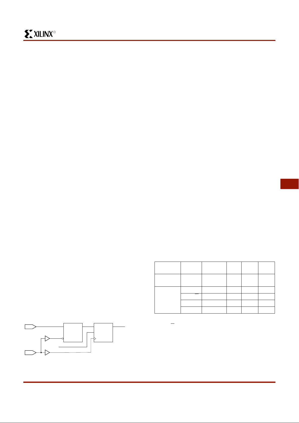
Registered Inputs
The I1 and I2 signals that exit the block can each carry
either the direct or registered input signal.
The input and output storage elements in each IOB have a
common clock enable input, which, through configuration,
can be activated individually for the input or output flip-flop,
or both. This clock enable operates exactly like the EC pin
on the XC4000 Series CLB. It cannot beinverted within the
IOB.
The storage element behavior is shown in Table 9.
Table 9: Input Register Functionality
(active rising edge is shown)
Optional Delay Guarantees Zero Hold Time
The data input to the register can optionally be delayed by
several nanoseconds. With the delay enabled, the setup
time of the input flip-flop is increased so that normal clock
routing does not result in a positive hold-time requirement.
A positive hold time requirement can lead to unreliable,
temperature- or processing-dependent operation.
The input flip-flop setup time is defined between the data
measured at the device I/O pin and the clock input at the
IOB (not at the clock pin). Any routing delay from the device
clock pin to the clock input of the IOB must, therefore, be
subtracted from this setup time to arrive at the real setup
time requirement relative to the device pins. A short specified setup time might, therefore, result in a negative setup
time at the device pins, i.e., a positive hold-time requirement.
When a delay is inserted on the data line, more clock delay
can be tolerated without causing a positive hold-time
requirement. Sufficient delay eliminates the possibility of a
data hold-time requirement at the external pin. The maximum delay is therefore inserted as the default.
The XC4000E IOB has a one-tap delay element: either the
delay is inserted (default), or it isnot. The delay guarantees
a zero hold time with respect to clocks routed through any
of the XC4000E global clock buffers.(See“Global Nets and
Buffers(XC4000E only)” on page 35 foradescriptionof the
global clock buffers in the XC4000E.) For a shorter input
register setup time,with non-zero hold, attach a NODELAY
attribute or property to the flip-flop.
The XC4000X IOB has a two-tap delay element, with
choices of a full delay, a partial delay, or no delay. The
attributes or properties used to select the desired delay are
shown in Table 10. The choices are no added attribute,
MEDDELAY, and NODELAY. The default setting, with no
added attribute, ensures no hold timewith respect to any of
the XC4000X clock buffers,including the Global Low-Skew
buffers. MEDDELAY ensures no hold time with respect to
the Global Early buffers. Inputs with NODELAYmayhavea
positive hold time with respect to all clock buffers. For a
description of each of these buffers, see “Global Nets and
Buffers (XC4000X only)” on page 37.
Table 10: XC4000X IOB Input Delay Element
Table 8: Supported Sources for XC4000 Series Device
Inputs
Source
XC4000E/EX
Series Inputs
XC4000XL
Series Inputs
5 V,
TTL
5 V,
CMOS
3.3 V
CMOS
Any device, Vcc = 3.3 V,
CMOS outputs
√
Unreli
-able
Data
√
XC4000 Series, Vcc = 5 V,
TTL outputs
√√
Any device, Vcc = 5 V,
TTL outputs (Voh ≤ 3.7 V)
√√
Any device, Vcc = 5 V,
CMOS outputs
√√ √
Mode Clock
Clock
Enable
DQ
Power-Up or
GSR
XXXSR
Flip-Flop __/
1* D D
0XXQ
Latch 1 1* X Q
01*DD
Both X 0 X Q
Legend:
X
__/
SR
0*
1*
Don’t care
Rising edge
Set or Reset value. Reset is default.
Input is Low or unconnected (default value)
Input is High or unconnected (default value)
Value When to Use
full delay
(default, no
attribute added)
Zero Hold with respect to Global
Low-Skew Buffer, Global Early Buffer
MEDDELAY ZeroHold with respecttoGlobal Early
Buffer
NODELAY Short Setup, positive Hold time
R
May 14, 1999 (Version 1.6) 6-23
XC4000E and XC4000X Series Field Programmable Gate Arrays
6
Additional Input Latch for FastCapture (XC4000X only)
The XC4000X IOB has an additional optional latch on the
input. This latch, as shown in Figure 16, is clocked by the
output clock — the clock used for the output flip-flop —
rather than the input clock. Therefore, two different clocks
can be used to clock the two input storage elements. This
additional latch allows the very fast capture of input data,
which is then synchronized to the internal clock by the IOB
flip-flop or latch.
To use this Fast Capture technique, drive the output clock
pin (the FastCapturelatchingsignal)fromtheoutput of one
of the Global Early buffers supplied in the XC4000X. The
second storage element should be clocked by a Global
Low-Skew buffer, to synchronize the incoming data to the
internal logic. (See Figure 17.) These special buffers are
described in “Global Nets and Buffers (XC4000X only)” on
page 37.
The Fast Capture latch (FCL) is designed primarily for use
with a Global Early buffer. For Fast Capture, a single clock
signal is routed through both a Global Early buffer and a
Global Low-Skew buffer. (The two buffers share an input
pad.) The Fast Capture latch is clocked by the Global Early
buffer, and the standard IOB flip-flop or latch is clocked by
the Global Low-Skew buffer.This mode is the safest way to
use the Fast Capture latch, because the clock buffers on
both storageelementsaredrivenbythesamepad.Thereis
no external skew between clock pads to create potential
problems.
To place the Fast Capture latch in a design, use one of the
special library symbols, ILFFX or ILFLX. ILFFX is a transparent-Low Fast Capture latch followed by an active-High
input flip-flop. ILFLX is a transparent-Low Fast Capture
latch followed by a transparent-High input latch. Any of the
clock inputs can be inverted before driving the library element, and the inverter is absorbed into the IOB. If a single
BUFG output is used to drive both clock inputs, the software automatically runs the clock through both a Global
Low-Skew buffer and a Global Early buffer, and clocks the
Fast Capture latch appropriately.
Figure 16 on page 21 also shows a two-tap delay on the
input. By default, if the Fast Capture latch is used, the Xilinx
software assumes a Global Early bufferis driving the clock,
and selects MEDDELAY to ensure a zero hold time. Select
the desired delay based on the discussion in the previous
subsection.
IOB Output Signals
Output signals can be optionally inverted within the IOB,
and can pass directly to the pad or be stored in an
edge-triggered flip-flop. The functionality of this flip-flop is
shown in Table 11.
An active-High 3-state signal can be used to place the output buffer in a high-impedance state, implementing 3-state
outputs or bidirectional I/O. Under configuration control, the
output (OUT) and output 3-state (T) signals can be
inverted. The polarity of these signals is independently configured for each IOB.
The 4-mA maximum output current specification of many
FPGAs often forces the user to add external buffers, which
are especially cumbersome on bidirectional I/O lines. The
XC4000E and XC4000EX/XL devices solve many of these
problems by providing a guaranteed output sink current of
12 mA. Two adjacent outputs can be interconnected externally to sink up to 24 mA. The XC4000E and XC4000EX/XL
FPGAs can thus directly drive buses on a printed circuit
board.
By default, the output pull-up structure is configured as a
TTL-liketotem-pole.TheHighdriverisann-channelpull-up
transistor, pulling to a voltage one transistor threshold
below Vcc. Alternatively, the outputs can beglobally configured as CMOS drivers, with p-channel pull-up transistors
pulling to Vcc. This option,applied using the bitstream generation software, applies to all outputs on the device. It is
not individually programmable. In the XC4000XL, all outputs are pulled to the positive supply rail.
IPAD
IPAD
BUFGE
BUFGLS
C
CE
DQ
GF
to internal
logic
ILFFX
X9013
Figure 17: Examples Using XC4000X FCL
Table 11: Output Flip-Flop Functionality (active rising
edge is shown)
Mode Clock
Clock
Enable T D Q
Power-Up
or GSR
X X 0* X SR
Flip-Flop
X00*XQ
__/
1* 0* D D
XX1XZ
0X0*XQ
Legend:
X
__/
SR
0*
1*
Z
Don’t care
Rising edge
Set or Reset value. Reset is default.
Input is Low or unconnected (default value)
Input is High or unconnected (default value)
3-state
R
XC4000E and XC4000X Series Field Programmable Gate Arrays
6-24 May 14, 1999 (Version 1.6)
Any XC4000 Series 5-Volt device with its outputs configured in TTL mode can drive the inputs of any typical
3.3-Volt device. (For a detailed discussion of how to interface between 5 V and 3.3 V devices, see the 3V Products
section of
The Programmable Logic Data Book
.)
Supported destinations for XC4000 Series device outputs
are shown in Table 12.
An output can be configured as open-drain (open-collector)
by placing an OBUFT symbol in a schematic or HDL code,
then tying the 3-state pin (T) to the output signal, and the
input pin (I) to Ground. (See Figure 18.)
Table 12: Supported Destinations for XC4000 Series
Outputs
Output Slew Rate
The slew rate of each output buffer is, by default, reduced,
to minimize power bus transients when switching non-critical signals. For critical signals, attach a FAST attribute or
property to the output buffer or flip-flop.
For XC4000E devices, maximum total capacitive load for
simultaneous fast mode switching in the same direction is
200 pF for all package pins between each Power/Ground
pin pair. For XC4000X devices, additional internal
Power/Ground pin pairs are connected to special Power
and Ground planes within the packages, to reduce ground
bounce. Therefore, the maximum total capacitive load is
300 pF between each external Power/Ground pin pair.
Maximum loading may vary for the low-voltage devices.
Forslew-ratelimitedoutputs this total is two times larger for
each device type: 400 pF for XC4000E devices and 600 pF
for XC4000X devices. This maximum capacitive load
should not be exceeded, as it can result in ground bounce
of greater than 1.5 V amplitude and more than 5 ns duration. This level of ground bounce may cause undesired
transient behavior on an output, or in the internal logic. This
restriction is common to all high-speed digital ICs, and is
not particular to Xilinx or the XC4000 Series.
XC4000 Series devices have a feature called “Soft
Start-up,” designed to reduce ground bounce when all outputs are turned on simultaneously at the end of configuration. When the configuration process is finished and the
device starts up, the first activation of the outputs is automatically slew-rate limited. Immediately following the initial
activation of the I/O, the slew rate of the individual outputs
is determined by the individual configurationoptionforeach
IOB.
Global Three-State
A separate Global 3-State line (not shown in Figure 15 or
Figure 16) forces all FPGA outputs to the high-impedance
state, unless boundary scan is enabled and is executing an
EXTEST instruction. This global net (GTS) does not compete with other routing resources; ituses a dedicated distribution network.
GTS can be driven from any user-programmable pin as a
global 3-state input. To use this global net, place an input
pad and input buffer in the schematic or HDL code, driving
the GTS pin of the STARTUP symbol. A specific pin location can be assigned to this input using a LOC attribute or
property,justaswithanyotheruser-programmablepad.An
inverter can optionally be inserted after the input buffer to
invert the sense of the Global 3-State signal. Using GTS is
similar to GSR. See Figure 2 on page 11 for details.
Alternatively, GTS can be driven from any internal node.
Destination
XC4000 Series
Outputs
3.3 V,
CMOS
5 V,
TTL
5 V,
CMOS
Any typical device,Vcc=3.3V,
CMOS-threshold inputs
√√some
1
1. Only if destination device has 5-V tolerant inputs
Any device, Vcc = 5 V,
TTL-threshold inputs
√√√
Any device, Vcc = 5 V,
CMOS-threshold inputs
Unreliable
Data
√
X6702
OPAD
OBUFT
Figure 18: Open-Drain Output
R
May 14, 1999 (Version 1.6) 6-25
XC4000E and XC4000X Series Field Programmable Gate Arrays
6
Output Multiplexer/2-Input Function Generator
(XC4000X only)
As shown in Figure 16 on page 21, the output path in the
XC4000X IOB contains an additional multiplexer not available in the XC4000E IOB. The multiplexer can also be configured as a 2-input function generator, implementing a
pass-gate,AND-gate,OR-gate,orXOR-gate,with0,1,or2
inverted inputs. The logic used to implement these functions is shown in the upper gray area of Figure 16.
When configured as a multiplexer, this feature allows two
output signals to time-share the same output pad; effectively doubling the number of device outputs without requiring a larger, more expensive package.
When the MUX is configured as a 2-input function generator, logic can be implemented within the IOB itself. Combined with a Global Early buffer, this arrangement allows
very high-speed gating of a single signal. For example, a
wide decoder can be implemented in CLBs, and its output
gated with a Read or Write Strobe Driven by a BUFGE
buffer, as shown in Figure 19. The critical-path pin-to-pin
delay of this circuit is less than 6 nanoseconds.
As shown in Figure 16, the IOB input pins Out, Output
Clock, and Clock Enable have different delays and different
flexibilities regarding polarity. Additionally, Output Clock
sources are more limited than the other inputs. Therefore,
the Xilinx software does not move logic into the IOB function generators unless explicitly directed to do so.
The user can specify that the IOB function generator be
used, by placing special library symbols beginning with the
letter “O.” Forexample, a 2-input AND-gate in the IOB function generator is called OAND2. Use the symbol input pin
labelled “F” for the signal on the critical path. This signal is
placed on the OK pin — the IOB input with the shortest
delay to the function generator. Two examples are shown in
Figure 20.
Other IOB Options
There are a number of other programmable options in the
XC4000 Series IOB.
Pull-up and Pull-down Resistors
Programmable pull-up and pull-down resistors are useful
for tying unused pins to Vcc or Ground to minimize power
consumption and reduce noise sensitivity.Theconfigurable
pull-up resistor is a p-channel transistor that pulls to Vcc.
The configurable pull-down resistor is an n-channel transistor that pulls to Ground.
The value of these resistors is 50 kΩ−100 kΩ. This high
value makes them unsuitable as wired-AND pull-up resistors.
The pull-up resistors for most user-programmable IOBs are
active during the configuration process. See Table 22 on
page 58 for a list of pins with pull-ups active before and dur-
ing configuration.
After configuration, voltage levels of unused pads, bonded
or un-bonded, must be valid logic levels, to reduce noise
sensitivity and avoid excess current. Therefore, by default,
unused pads are configured with the internal pull-up resistor active. Alternatively, they can be individually configured
with the pull-down resistor, or as a driven output, or to be
driven by an external source. To activate the internal
pull-up, attach the PULLUP library component to the net
attached to the pad. To activate the internal pull-down,
attach the PULLDOWN library component to the net
attached to the pad.
Independent Clocks
Separate clocksignalsareprovidedfortheinputandoutput
flip-flops. The clock can be independently inverted for each
flip-flop within the IOB, generating either falling-edge or rising-edge triggered flip-flops. The clock inputs for each IOB
are independent, except that in the XC4000X, the Fast
Capture latch shares an IOB input withtheoutput clock pin.
Early Clock for IOBs (XC4000X only)
Special early clocks are available for IOBs. These clocks
are sourced by the same sources as the Global Low-Skew
buffers,but are separately buffered.They have fewer loads
and therefore less delay. The early clock can drive either
the IOB output clock or the IOB input clock, or both. The
early clock allows fast capture of input data, and fast
clock-to-output on output data. The Global Early buffers
that drive these clocks are described in “Global Nets and
Buffers (XC4000X only)” on page 37.
Global Set/Reset
As with the CLB registers, the Global Set/Reset signal
(GSR) can be used to set or clear the input and output registers, depending on the value of the INIT attribute or property. The two flip-flops can be individually configured to set
IPAD
F
OPAD
FAST
BUFGE
OAND2
from
internal
logic
X9019
Figure 19: Fast Pin-to-Pin Path in XC4000X
OAND2
F
X6598
D0
S0
D1
O
OMUX2
X6599
Figure 20: AND & MUX Symbols in XC4000X IOB

R
XC4000E and XC4000X Series Field Programmable Gate Arrays
6-26 May 14, 1999 (Version 1.6)
or clear on reset and after configuration. Other than the global GSR net, no user-controlled set/resetsignal is available
to the I/O flip-flops. The choice of set or clear applies to
both the initial state of the flip-flop and the response to the
Global Set/Reset pulse. See “Global Set/Reset” on
page 11 for a description of how to use GSR.
JTAG Support
Embedded logic attached to the IOBs contains test structures compatible with IEEE Standard 1149.1 for boundary
scan testing, permitting easy chip and board-level testing.
More information is provided in “Boundary Scan” on
page 42.
Three-State Buffers
A pair of 3-state buffers is associated with each CLB in the
array. (See Figure 27 on page 30.) These 3-state buffers
can be used to drive signals onto the nearest horizontal
longlines above and below the CLB. They can thereforebe
used to implement multiplexedor bidirectional buses on the
horizontal longlines, saving logic resources. Programmable
pull-up resistors attached to these longlines help to implement a wide wired-AND function.
The buffer enable is an active-High 3-state (i.e. an
active-Low enable), as shown in Table 13.
Another 3-state buffer with similar access is located near
each I/O block along the right and left edges of the array.
(See Figure 33 on page 34.)
The horizontal longlines driven by the 3-state buffers have
a weak keeper at each end. This circuit preventsundefined
floating levels. However, it is overridden by any driver, even
a pull-up resistor.
Special longlines running along the perimeter of the array
can be used to wire-AND signals coming fromnearby IOBs
or from internal longlines. These longlines form the wide
edge decoders discussed in “Wide Edge Decoders” on
page 27.
Three-State Buffer Modes
The 3-state buffers can be configured in three modes:
• Standard 3-state buffer
• Wired-AND with input on the I pin
• Wired OR-AND
Standard 3-State Buffer
All three pins are used. Place the library element BUFT.
Connect the input to the I pin and the output to the O pin.
The T pin is an active-High 3-state (i.e. an active-Low
enable). Tie the T pin to Ground to implement a standard
buffer.
Wired-AND with Input on the I Pin
The buffer can be used as a Wired-AND. Use the WAND1
library symbol, which is essentially an open-drain buffer.
WAND4,WAND8, and WAND16arealsoavailable. See the
XACT Libraries Guide
for further information.
The T pin is internally tied to the I pin. Connect the input to
the I pin and theoutput to the O pin. Connectthe outputs of
all the WAND1s together and attach a PULLUP symbol.
Wired OR-AND
The buffer can be configured as a Wired OR-AND. A High
level on either input turns off the output. Use the
WOR2AND library symbol, which is essentially an
open-drain 2-input OR gate. The two input pins are functionally equivalent. Attach the two inputs to the I0 and I1
pins and tie the output to the O pin. Tie the outputs ofallthe
WOR2ANDs together and attach a PULLUP symbol.
Three-State Buffer Examples
Figure 21 shows how to use the 3-state buffers to imple-
ment a wired-AND function. When all the buffer inputs are
High, the pull-up resistor(s) provide the High output.
Figure 22 shows how to use the 3-state buffers to imple-
ment a multiplexer. The selection is accomplished by the
buffer 3-state signal.
Pay particular attention to the polarity of the T pin when
using these buffers in a design. Active-High 3-state (T) is
identical to an active-Low output enable, as shown in
Table 13.
Table 13: Three-State Buffer Functionality
IN T OUT
X1Z
IN 0 IN
P
U
L
L
U
P
Z = D
A
●
D
B
●
(DC+DD) ● (DE+DF)
D
E
D
F
D
C
D
D
D
B
D
A
WAND1 WAND1
WOR2AND WOR2AND
X6465
Figure 21: Open-Drain Buffers Implement a Wired-AND Function

R
May 14, 1999 (Version 1.6) 6-27
XC4000E and XC4000X Series Field Programmable Gate Arrays
6
Wide Edge Decoders
Dedicated decoder circuitry boosts the performance of
wide decoding functions. When the address or data field is
wider than the function generator inputs, FPGAs need
multi-level decoding and are thus slower than PALs.
XC4000 Series CLBs have nine inputs. Any decoder of up
to nine inputs is, therefore, compact and fast. However,
there is also a need for much wider decoders, especially for
address decoding in large microprocessor systems.
An XC4000 Series FPGA has four programmable decoders
located on each edge of the device. The inputs to each
decoder are any of the IOB I1 signals on that edgeplusone
local interconnect per CLB row or column. Each row or column of CLBs provides up to three variables or their compliments., as shown in Figure 23. Each decoder generates a
High output (resistor pull-up) when the AND condition of
the selected inputs, or their complements, is true. This is
analogous to a product term in typical PAL devices.
Each of these wired-AND gates is capable of accepting up
to 42 inputs on the XC4005E and 72 on the XC4013E.
There are up to 96 inputs for each decoder on the
XC4028X and 132 on the XC4052X. The decoders may
also be split in two when a larger number of narrower
decoders are required, for a maximum of 32 decoders per
device.
The decoder outputs can drive CLB inputs, so they can be
combined with other logic to form a PAL-likeAND/OR structure. The decoder outputs canalso be routed directly tothe
chip outputs. For fastestspeed,the output should be on the
same chip edge as the decoder. Very large PALs can be
emulated by ORing the decoder outputs in a CLB. This
decoding feature covers what has long been considered a
weakness of older FPGAs. Users oftenresorted to external
PALs for simple but fast decoding functions. Now, the dedicated decoders in the XC4000 Series device can implement these functions fast and efficiently.
To use the wide edge decoders, place one or more of the
WAND library symbols (WAND1, WAND4, WAND8,
WAND16). Attach a DECODE attribute or property to each
WAND symbol. Tie the outputs together and attach a PUL-
LUP symbol. Location attributes or properties such as L
(left edge) or TR (right half of top edge) should also beused
to ensure the correct placement of the decoder inputs.
On-Chip Oscillator
XC4000 Series devices include an internal oscillator. This
oscillator is used to clock the power-on time-out, for configuration memory clearing, and as the source of CCLK in
Master configuration modes. The oscillator runs at a nominal 8 MHz frequency that varies with process, Vcc, and
temperature. The output frequency falls between 4 and 10
MHz.
D
N
D
C
D
B
D
A
ABCN
Z = DA • A + DB • B + DC • C + DN • N
~100 kΩ
"Weak Keeper"
X6466
BUFT BUFT BUFT BUFT
Figure 22: 3-State Buffers Implement a Multiplexer
IOB
IOB
BA
INTERCONNECT
( C) .....
(A • B • C) .....
(A • B • C) .....
(A • B • C) .....
.I1.I1
X2627
C
Figure 23: XC4000 Series Edge Decoding Example
F16K
F500K
F8M
F490
F15
X6703
OSC4
Figure 24: XC4000 Series Oscillator Symbol

R
XC4000E and XC4000X Series Field Programmable Gate Arrays
6-28 May 14, 1999 (Version 1.6)
The oscillator output is optionally available after configuration. Any twoof fourresynchronizedtapsofabuilt-individer
are also available. These taps are at the fourth, ninth, fourteenth and nineteenth bits of the divider. Therefore, if the
primary oscillator output is running at the nominal 8 MHz,
the user has access to an 8 MHz clock, plusany two of 500
kHz, 16kHz, 490Hz and 15Hz (upto 10% lower forlow-voltage devices). These frequencies can vary by as much as
-50% or +25%.
These signals can be accessed by placing the OSC4
library element in a schematic or in HDL code (see
Figure 24).
The oscillator is automatically disabledafter configuration if
the OSC4 symbol is not used in the design.
Programmable Interconnect
All internal connections are composed of metal segments
with programmableswitchingpointsandswitchingmatrices
to implement the desired routing. A structured, hierarchical
matrix of routing resources is provided to achieve efficient
automated routing.
The XC4000E and XC4000X share a basic interconnect
structure. XC4000X devices, however,haveadditionalrouting not available in the XC4000E. The extra routing
resources allow high utilization in high-capacity devices. All
XC4000X-specific routing resources are clearly identified
throughout this section. Any resources not identified as
XC4000X-specific are present in all XC4000 Series
devices.
This section describes the varied routing resources available in XC4000 Series devices. The implementation software automatically assigns the appropriate resources
based on the density and timing requirements of the
design.
Interconnect Overview
There are several types of interconnect.
• CLB routing is associated with each row and column of
the CLB array.
• IOB routing forms a ring (called a VersaRing) around
the outside of the CLB array. It connects theI/O with the
internal logic blocks.
• Global routing consists of dedicated networks primarily
designed to distribute clocksthroughout the device with
minimum delay and skew. Global routing can also be
used for other high-fanout signals.
Five interconnect types are distinguished by the relative
length of their segments: single-length lines, double-length
lines, quad and octal lines (XC4000X only), and longlines.
In the XC4000X, direct connects allow fast data flow
between adjacent CLBs, and between IOBs and CLBs.
Extra routing is included in the IOB pad ring. The XC4000X
also includes a ring of octal interconnect lines near the
IOBs to improve pin-swapping and routing to locked pins.
XC4000E/X devices include two types of global buffers.
These global buffers have different properties, and are
intended for different purposes. They are discussed in
detail later in this section.
CLB Routing Connections
A high-level diagram of the routing resources associated
with one CLB is shown in Figure 25. The shaded arrows
represent routing present only in XC4000X devices.
Table 14 shows how much routing of each type is available
in XC4000E and XC4000X CLB arrays. Clearly, very large
designs, or designs with a great deal of interconnect, will
route more easily in the XC4000X. Smaller XC4000E
designs, typically requiring significantly less interconnect,
do not require the additional routing.
Figure 27 on page 30 is a detailed diagram of both the
XC4000E and the XC4000X CLB, with associated routing.
The shaded square is the programmable switch matrix,
present in both the XC4000E and the XC4000X. The
L-shaped shaded area is present only in XC4000X devices.
As shown in the figure, the XC4000Xblockisessentially an
XC4000E block with additional routing.
CLB inputs and outputs are distributed on all four sides,
providing maximum routing flexibility. In general, the entire
architecture is symmetrical and regular. It is well suited to
established placement and routing algorithms. Inputs, outputs, and function generators can freely swap positions
within a CLB to avoid routing congestion during the placement and routing operation.

R
May 14, 1999 (Version 1.6) 6-29
XC4000E and XC4000X Series Field Programmable Gate Arrays
6
Table 14: Routing per CLB in XC4000 Series Devices
Programmable Switch Matrices
The horizontal and vertical single- and double-length lines
intersect at a box called a programmable switch matrix
(PSM). Each switch matrix consists of programmable pass
transistors used to establishconnections between the lines
(see Figure 26).
For example, a single-length signal entering on the right
side of the switch matrix can be routed to a single-length
line on the top, left, or bottom sides, or any combination
thereof, if multiple branches are required. Similarly, a double-length signal can be routed to a double-length line on
any or all of the other three edges of the programmable
switch matrix.
Single-Length Lines
Single-length lines provide the greatest interconnect flexibility and offer fast routing between adjacent blocks. There
are eight vertical and eight horizontal single-length lines
associated with each CLB. These lines connect the switching matrices that are located in every row and a column of
CLBs.
Single-length lines are connected by way of the programmable switch matrices, as shown in Figure 28. Routing
connectivity is shown in Figure 27.
Single-length lines incur a delay whenever they go through
a switching matrix. Therefore, they are not suitable for routing signals for long distances. They are normally used to
conduct signals within a localized area and to provide the
branching for nets with fanout greater than one.
x5994
Quad
Quad
Single
Double
Long
Direct
Connect
Long
CLB
Long Global
Clock
Long Double Single Global
Clock
Carry
Chain
Direct
Connect
Figure 25: High-Level Routing Diagram of XC4000 Series CLB (shaded arrows indicate XC4000X only)
XC4000E XC4000X
Vertical Horizontal Vertical Horizontal
Singles 8 8 8 8
Doubles 4 4 4 4
Quads 0 0 12 12
Longlines 6 6 10 6
Direct
Connects
0022
Globals 4 0 8 0
Carry Logic 2 0 1 0
Total 24 18 45 32
Six Pass Transistors
Per Switch Matrix
Interconnect Point
Singles
Double
Double
Singles
Double
Double
X6600
Figure 26: Programmable Switch Matrix (PSM)

R
XC4000E and XC4000X Series Field Programmable Gate Arrays
6-30 May 14, 1999 (Version 1.6)
F1
C1
G1
F2
C2
G2
F3
C3
G3
F4
C4
G4
K
X
Y
XQ
YQ
LONG
SINGLE
DOUBLE
LONG
GLOBAL
QUAD
LONG
SINGLE
DOUBLE
LONG
LONG
DOUBLE
DOUBLE
QUAD
GLOBAL
Common to XC4000E and XC4000X
XC4000X only
Programmable Switch Matrix
CLB
DIRECT
FEEDBACK
DIRECT
FEEDBACK
Figure 27: Detail of Programmable Interconnect Associated with XC4000 Series CLB

R
May 14, 1999 (Version 1.6) 6-31
XC4000E and XC4000X Series Field Programmable Gate Arrays
6
Double-Length Lines
The double-lengthlinesconsistofagridofmetalsegments,
each twice as long as the single-length lines: they run past
two CLBs before entering a switch matrix. Double-length
lines are grouped in pairs with the switch matrices staggered, so that each line goes through a switch matrix at
every other row or column of CLBs (see Figure 28).
There are four vertical and four horizontal double-length
lines associated with each CLB. These lines provide faster
signal routing over intermediate distances, while retaining
routing flexibility. Double-length lines are connected by way
of the programmable switch matrices. Routing connectivity
is shown in Figure 27.
Quad Lines (XC4000X only)
XC4000X devices also include twelve vertical and twelve
horizontal quad lines per CLB row and column. Quad lines
are four times as long as the single-length lines. They are
interconnected via buffered switch matrices (shown as diamonds in Figure 27 on page 30). Quad lines run past four
CLBs before entering a buffered switch matrix. They are
grouped in fours, with the buffered switch matrices staggered, so that each line goes through a buffered switch
matrix at every fourth CLB location in that row or column.
(See Figure 29.)
The buffered switch matrixes have four pins, one on each
edge. All of the pins are bidirectional. Any pin candrive any
or all of the other pins.
Each buffered switch matrix contains one buffer and six
pass transistors. It resembles the programmable switch
matrix shown in Figure 26, with the addition of a programmable buffer. There can be up to two independent inputs
and up to two independent outputs. Only one of the independent inputs can be buffered.
The place and route software automatically uses the timing
requirements of the design to determine whether or not a
quad line signal should be buffered. A heavily loaded signal
is typically buffered, while a lightly loaded one is not. One
scenario is to alternate buffers and pass transistors. This
allows both vertical and horizontal quad lines tobebuffered
at alternating buffered switch matrices.
Due to the buffered switch matrices, quad lines are very
fast. They provide the fastest available method of routing
heavily loaded signals for long distances across the device.
Longlines
Longlines form a grid of metal interconnect segments that
run the entire length or width of the array. Longlines are
intended for high fan-out, time-critical signal nets, or nets
that are distributed over long distances. In XC4000X
devices, quad lines are preferred for critical nets, because
the buffered switch matrices make them faster for high
fan-out nets.
Two horizontal longlines per CLB can be driven by 3-state
or open-drain drivers (TBUFs). They can therefore implement unidirectional or bidirectional buses, wide multiplexers, or wired-AND functions. (See “Three-State Buffers” on
page 26 for more details.)
Each horizontal longline driven by TBUFs has either two
(XC4000E) or eight (XC4000X) pull-up resistors. To activate these resistors, attach a PULLUP symbol to the
long-line net. The software automatically activates the
appropriate number of pull-ups. There is also a weak
keeper at each end of these two horizontal longlines. This
CLB
PSM PSM
PSMPSM
CLB CLB
CLB CLB CLB
CLB CLB CLB
Doubles
Singles
Doubles
X6601
Figure 28: Single- and Double-Length Lines, with
Programmable Switch Matrices (PSMs)
CLB
CLB
CLB
CLB
CLB
CLB
CLB
CLB
CLB
X9014
Figure 29: Quad Lines (XC4000X only)

R
XC4000E and XC4000X Series Field Programmable Gate Arrays
6-32 May 14, 1999 (Version 1.6)
circuit prevents undefined floating levels. However, it is
overridden by any driver, even a pull-up resistor.
Each XC4000E longline has a programmablesplitterswitch
at its center, as does each XC4000X longline driven by
TBUFs. This switch can separate the line into two independent routing channels, each running half the widthor height
of the array.
Each XC4000X longline not driven by TBUFs has a buffered programmable splitter switch at the 1/4, 1/2, and 3/4
points of the array. Due to the buffering, XC4000X longline
performance does not deteriorate with the larger array
sizes. If the longline is split, the resulting partial longlines
are independent.
Routing connectivity of the longlines is shown in Figure 27
on page 30.
Direct Interconnect (XC4000X only)
The XC4000X offers two direct, efficient and fast connections between adjacent CLBs. These nets facilitate a data
flow from the left to the right side of the device, or from the
top to the bottom, as shown in Figure 30. Signals routed on
the direct interconnect exhibit minimum interconnect propagation delay and use no general routing resources.
The direct interconnect is also present between CLBs and
adjacent IOBs. Each IOB on the left and top device edges
has a direct path to the nearestCLB.EachCLB on the right
and bottom edges of the array has a direct path tothenearest two IOBs, since there are two IOBs for each row or column of CLBs.
The place and route software uses direct interconnect
wheneverpossible, to maximize routing resources and minimize interconnect delays.
I/O Routing
XC4000 Series devices have additional routing around the
IOB ring. This routing iscalled a VersaRing.TheVersaRing
facilitates pin-swapping and redesign without affecting
board layout. Included are eight double-length lines spanning two CLBs (four IOBs), and four longlines. Global lines
and Wide Edge Decoder lines are provided. XC4000X
devices also include eight octal lines.
A high-level diagram of the VersaRing is shown in
Figure 31. The shaded arrows represent routing present
only in XC4000X devices.
Figure 33 on page 34 isadetaileddiagramoftheXC4000E
and XC4000X VersaRing. The area shown includes two
IOBs. There are two IOBs per CLB row or column, therefore this diagram corresponds to the CLB routing diagram
shown in Figure 27 on page 30. The shaded areas represent routing and routing connections present only in
XC4000X devices.
Octal I/O Routing (XC4000X only)
Between the XC4000X CLB array and the pad ring, eight
interconnect tracks provide for versatility in pin assignment
and fixed pinout flexibility. (See Figure 32 on page 33.)
These routing tracks are called octals, because they can be
broken every eight CLBs (sixteen IOBs) by a programmablebuffer that also functions as a splitter switch. The buffers
are staggered, so each line goes through a buffer at every
eighth CLB location around the device edge.
The octal lines bend around the corners of the device. The
lines cross at the corners in such a way that the segment
most recently buffered before the turn has the farthest distance to travel before the next buffer, as shown in
Figure 32.
CLB
IOB
X6603
IOB
IOB
IOB
IOB
IOB
IOB
IOB
IOB
IOB
IOB
IOB
IOB
IOB
IOB
IOB
IOB
IOB
IOB
IOB
CLB
CLB
CLB
CLB
CLB
~
~
~
~
~
~
~
~
~
~
~
~
~
~
~
~
~
~
~
~
Figure 30: XC4000X Direct Interconnect
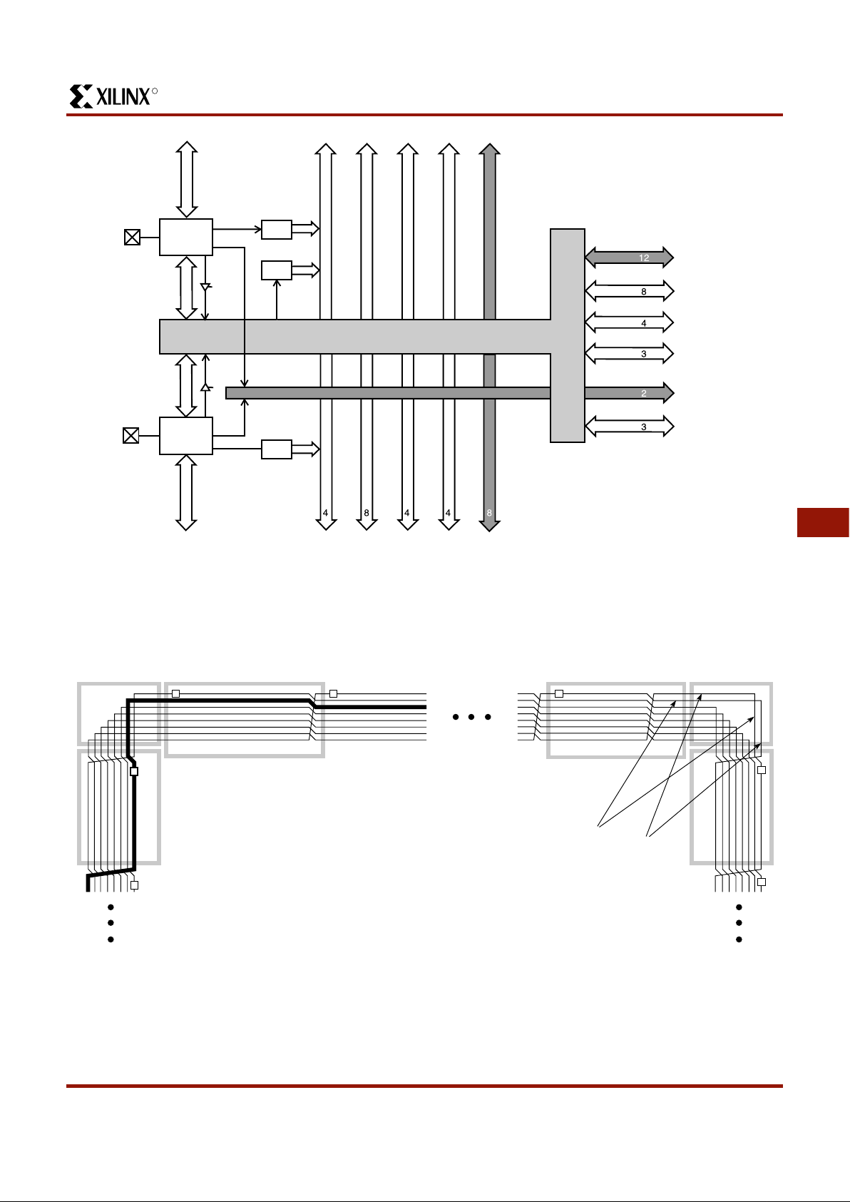
R
May 14, 1999 (Version 1.6) 6-33
XC4000E and XC4000X Series Field Programmable Gate Arrays
6
X5995
Direct
Connect
Edge
Decode
Double Long Global
Clock
Octal
Quad
Single
Double
Long
Direct
Connect
Long
INTERCONNECT
IOB
WED
WED
WED
IOB
Figure 31: High-Level Routing Diagram of XC4000 Series VersaRing (Left Edge)
WED = Wide Edge Decoder, IOB = I/O Block (shaded arrows indicate XC4000X only)
Segment with nearest buffer
connects to segment with furthest buffer
IOB
IOB
IOB
IOB
X9015
Figure 32: XC4000X Octal I/O Routing

R
XC4000E and XC4000X Series Field Programmable Gate Arrays
6-34 May 14, 1999 (Version 1.6)
T
O
C
L
B
A
R
R
A
Y
IK
OK
I1CEI2
DECODER
T
O
OCTAL
EDGE
DECODE
QUAD
LONG
SINGLE
DOUBLE
LONG
LONG
DOUBLE
DOUBLE
GLOBAL
IK
OK
I1
CE
I2
T
O
DECODER DECODER
Common to XC4000E and XC4000X
XC4000X only
IOB
IOB
DIRECT
Figure 33: Detail of Programmable Interconnect Associated with XC4000 Series IOB (Left Edge)

R
May 14, 1999 (Version 1.6) 6-35
XC4000E and XC4000X Series Field Programmable Gate Arrays
6
IOB inputs and outputs interface with the octal lines via the
single-length interconnect lines. Single-length lines are
also used for communication between the octals and double-length lines, quads, and longlines within the CLB array.
Segmentation into buffered octals was found to be optimal
for distributing signals over long distances around the
device.
Global Nets and Buffers
Both the XC4000E and the XC4000X have dedicated global networks. These networks are designed to distribute
clocks and other high fanout control signals throughout the
devices with minimal skew. The global buffers are
described in detail in the following sections. The text
descriptions and diagrams are summarized in Table 15.
The table shows which CLB and IOB clock pins can be
sourced by which global buffers.
In both XC4000E and XC4000X devices, placement of a
library symbol called BUFG results in the software choosing the appropriate clock buffer, based on the timing
requirements of the design. The detailed information in
these sections is included only for reference.
Global Nets and Buffers (XC4000E only)
Four vertical longlines in each CLB column are driven
exclusively by special global buffers. These longlines are
in addition to the vertical longlines used for standard interconnect. The four global lines can be driven by either of two
types of global buffers. The clock pins of every CLB and
IOB can also be sourced from local interconnect.
Two different types of clock buffers are available in the
XC4000E:
• Primary Global Buffers (BUFGP)
• Secondary Global Buffers (BUFGS)
Four Primary Global buffers offer the shortest delay and
negligible skew. Four Secondary Global buffers have
slightly longer delay and slightly more skew due to potentially heavier loading, but offer greater flexibility when used
to drive non-clock CLB inputs.
The Primary Global buffers must be driven by the
semi-dedicated pads. The Secondary Global buffers can
be sourced byeither semi-dedicated pads or internal nets.
Each CLB column has four dedicated vertical Global lines.
Each of these lines can be accessed by one particular Primary Global buffer, or by any of the Secondary Global buffers, as shown in Figure 34. Each corner of the device has
one Primary buffer and one Secondary buffer.
IOBs along the left and right edges have four vertical global
longlines. Top and bottom IOBs can be clocked from the
global lines in the adjacent CLB column.
A global buffer should be specified for all timing-sensitive
global signal distribution. To use a global buffer, place a
BUFGP (primary buffer), BUFGS (secondary buffer), or
BUFG (either primary or secondary buffer) element in a
schematic or in HDL code. If desired, attach a LOC
attribute or property to direct placement to the designated
location. For example, attach a LOC=L attribute or property
to a BUFGS symbol to direct that a buffer be placed in one
of the two Secondary Global buffers on the left edge of the
device, or a LOC=BL to indicate the Secondary Global
buffer on the bottom edge of the device, on the left.
L = Left, R = Right, T = Top, B = Bottom
Table 15: Clock Pin Access
XC4000E XC4000X
Local
Inter-
connect
BUFGP BUFGS BUFGLS
L & R
BUFGE
T & B
BUFGE
All CLBs in Quadrant √√√√√√
All CLBs in Device √√√ √
IOBs on Adjacent Vertical
Half Edge
√√√√√√
IOBs on Adjacent Vertical
Full Edge
√√√√
√
IOBs on Adjacent Horizontal
Half Edge (Direct)
√ √
IOBs on Adjacent Horizontal
Half Edge (through CLB globals)
√√√√√√
IOBs on Adjacent Horizontal
Full Edge (through CLB globals)
√√√ √

R
XC4000E and XC4000X Series Field Programmable Gate Arrays
6-36 May 14, 1999 (Version 1.6)
X4 X4
X6604
X4
4
One BUFGP
per Global Line
One BUFGP
per Global Line
Any BUFGS Any BUFGS
BUFGP
PGCK4
SGCK4
PGCK3
SGCK3
BUFGS
BUFGP
BUFGS
IOB
IOB
IOBIOBIOBIOB
IOBIOBIOB
IOB
IOB
BUFGS
BUFGS
BUFGP
BUFGP
SGCK1
PGCK1
SGCK2
PGCK2
IOB
X4
locals
localslocals
locals
locals
locals
locals
locals
locals
locals
locals
locals
4
4
4
CLB
CLB
locals locals
CLB
CLB
locals
locals
Figure 34: XC4000E Global Net Distribution
X4
4
IOB
CLOCKS
CLB CLOCKS
(PER COLUMN)
CLB CLOCKS
(PER COLUMN)
CLB CLOCKS
(PER COLUMN)
CLB CLOCKS
(PER COLUMN)
locals
locals
locals
locals
locals
BUFGLS
locals
BUFGLS
BUFGLS
BUFGLS BUFGLS
BUFGE
BUFGE
BUFGE
BUFGE
BUFGE
BUFGE
BUFGE BUFGE
BUFGLS BUFGLS
IOB IOB IOB IOB
IOB IOB IOB IOB
BUFGLS BUFGLS
BUFGLS BUFGLS
GCK8 GCK7
GCK1 GCK6
GCK2 GCK5
GCK3
GCK4
IOB
IOB
IOB
IOB
locals
BUFGLS
locals
BUFGLS
locals
locals
BUFGLS
locals
BUFGLS
IOB
CLOCKS
IOB
CLOCKS
IOB
CLOCKS
4
X8
X8
X4
X9018
8
8
8 8
8
BUFGLS
locals
8
8 8
8 8
8
8
8
8
CLB
CLB
CLB
CLB
locals
locals
locals
locals
locals
locals
locals
locals
X8
X8
X8
X8
Figure 35: XC4000X Global Net Distribution

R
May 14, 1999 (Version 1.6) 6-37
XC4000E and XC4000X Series Field Programmable Gate Arrays
6
Global Nets and Buffers (XC4000X only)
Eight vertical longlines in each CLB column are driven by
special global buffers.These longlines are in addition to the
vertical longlines used for standard interconnect. The global lines are broken in the center of the array,toallowfaster
distribution and to minimize skew across the whole array.
Each half-column global line has its own buffered multiplexer, as shown in Figure 35. The top and bottom global
lines cannot be connected across the center of the device,
as this connection might introduce unacceptable skew. The
top and bottom halves of the global lines must be separately driven — although they can be driven by the same
global buffer.
The eight global lines in eachCLB column can be driven by
either of two types of global buffers. They can also be
driven by internal logic, because they can be accessed by
single, double, and quad lines at the top, bottom, half, and
quarter points. Consequently, the number of different
clocks that can be used simultaneously in an XC4000X
device is very large.
There are four global lines feedingthe IOBs at the left edge
of the device. IOBs along the right edge have eight global
lines. There is a single global line along the top and bottom
edges with access to the IOBs. All IOB globallines are broken at the center. They cannot be connected across the
center of the device, as this connection might introduce
unacceptable skew.
IOB global lines can be driven from two types of global buffers, or from local interconnect. Alternatively, top and bottom
IOBs can be clocked from the global lines in the adjacent
CLB column.
Two different types of clock buffers are available in the
XC4000X:
• Global Low-Skew Buffers (BUFGLS)
• Global Early Buffers (BUFGE)
Global Low-Skew Buffers are the standard clock buffers.
They should be used for most internal clocking, whenever a
large portion of the device must be driven.
Global Early Buffers are designed to provide a faster clock
access, but CLB access is limited to one-fourth of the
device. They also facilitate a faster I/O interface.
Figure 35 is a conceptual diagram of the global net struc-
ture in the XC4000X.
Global Early buffers and Global Low-Skew buffers share a
single pad. Therefore,thesame IPAD symbol can driveone
bufferof each type, in parallel. This configuration is particularly useful when using the Fast Capture latches, as
described in “IOB Input Signals” on page 20. PairedGlobal
Early and Global Low-Skew buffers share a common input;
they cannot be driven by two different signals.
Choosing an XC4000X Clock Buffer
The clocking structure of the XC4000X provides a large
variety of features. However, it can be simple to use, without understanding all the details. The software automatically handles clocks, along with all other routing, when the
appropriate clock buffer is placed in the design. In fact, if a
buffer symbol called BUFG is placed, rather than a specific
type of buffer, the software even chooses the buffer most
appropriate for the design. The detailed information in this
section is provided forthose users who want a finer level of
control over their designs.
If fine control is desired, use the following summary and
Table 15 on page 35 to choose an appropriate clock buffer.
• The simplest thing to do is to use a Global Low-Skew
buffer.
• If a faster clock path is needed, try a BUFG. The
software will first try to use aGlobal Low-SkewBuffer. If
timing requirements are not met, a faster buffer will
automatically be used.
• If a single quadrant of the chip is sufficient for the
clockedlogic,andthetimingrequiresafasterclock than
the Global Low-Skew buffer, use a Global Early buffer.
Global Low-Skew Buffers
Each corner of the XC4000X device has two Global
Low-Skew buffers. Any of the eight Global Low-Skew buffers can drive any of the eight vertical Global lines in a column of CLBs. In addition, any of the bufferscandriveany of
the four vertical lines accessing the IOBs on the leftedgeof
the device, and any of the eight vertical lines accessing the
IOBs on the right edge of the device. (See Figure 36 on
page 38.)
IOBs at the top and bottom edges of the device are
accessed through the vertical Global lines in the CLB array,
as in the XC4000E. Any Global Low-Skew buffer can,
therefore, access every IOB and CLB in the device.
The Global Low-Skew buffers can be driven by either
semi-dedicated pads or internal logic.
To use a Global Low-Skew buffer, instantiate a BUFGLS
element in a schematic or in HDL code. If desired, attach a
LOC attribute or property to direct placement to the designated location. For example, attach a LOC=T attribute or
property to direct that a BUFGLS be placed in one of the
two Global Low-Skewbuffersonthetop edge of the device,
or a LOC=TR to indicate the Global Low-Skew bufferonthe
top edge of the device, on the right.

R
XC4000E and XC4000X Series Field Programmable Gate Arrays
6-38 May 14, 1999 (Version 1.6)
Global Early Buffers
Each corner of the XC4000X device has two Global Early
buffers. The primary purpose of the Global Early buffers is
to provide an earlier clock access than the potentially
heavily-loaded Global Low-Skew buffers. A clock source
applied to both buffers will result in the Global Early clock
edge occurring several nanoseconds earlier than the Global Low-Skew buffer clock edge, due to the lighter loading.
Global Early buffers also facilitate the fast capture of device
inputs, using the Fast Capture latches described in “IOB
Input Signals” on page 20. For Fast Capture, take a single
clock signal, and route it through both a Global Early buffer
and a Global Low-Skew buffer. (The two buffers share an
input pad.) Use the Global Early buffer to clock the Fast
Capture latch, and the Global Low-Skewbufferto clock the
normal input flip-flop or latch, as shown in Figure 17 on
page 23.
The Global Early buffers can also be used to provide a fast
Clock-to-Outondeviceoutputpins. However, an early clock
in the output flip-flop IOB must be taken into consideration
when calculating the internal clock speed for the design.
The Global Early buffers at the left and right edges of the
chip have slightly different capabilities than the ones at the
top and bottom. Refer to Figure 37, Figure 38, and
Figure 35 on page 36 while reading the following explana-
tion.
Each Global Early buffer can access the eight vertical Glo-
bal lines for all CLBs in the quadrant. Therefore, only
one-fourth of the CLB clock pins can be accessed. This
restriction is in large part responsible for the faster speed of
the buffers, relative to the Global Low-Skew buffers.
The left-side Global Early bufferscan each drive two of the
fourvertical lines accessing the IOBs on the entire left edge
of the device. The right-side Global Early buffers can each
drive two of the eight vertical lines accessing the IOBs on
the entire right edge of the device. (See Figure 37.)
Each left and right Global Early buffer can also drive half of
the IOBs along either the top or bottom edge of the device,
using a dedicated line that can only be accessed through
the Global Early buffers.
The top and bottom Global Early buffers can drive half of
the IOBs along either the left or right edge of the device, as
shown in Figure 38. They can only access the top and bottom IOBs via the CLB global lines.
16
25
3
8
4
7
CLB CLB
CLBCLB
I
O
B
I
O
B
I
O
B
I
O
B
IOB IOB
IOBIOB
X6753
Figure 36: Any BUFGLS (GCK1 - GCK8) Can
Drive Any or All Clock Inputs on the Device
16
25
3
8
4
7
CLB CLB
CLBCLB
I
O
B
I
O
B
I
O
B
I
O
B
IOB IOB
IOBIOB
X6751
Figure 37: Left and Right BUFGEs Can Drive Any or
All Clock Inputs in Same Quadrant or Edge (GCK1 is
shown. GCK2, GCK5 and GCK6 are similar.)
16
25
3
8
4
7
CLB CLB
CLBCLB
I
O
B
I
O
B
I
O
B
I
O
B
IOB IOB
IOBIOB
X6747
Figure 38: Top and Bottom BUFGEs Can Drive Any
or All Clock Inputs in Same Quadrant (GCK8 is
shown. GCK3, GCK4 and GCK7 are similar.)

R
May 14, 1999 (Version 1.6) 6-39
XC4000E and XC4000X Series Field Programmable Gate Arrays
6
The top and bottom Global Early buffers are about 1 ns
slower clock to out than the left and right Global Early buffers.
The Global Early buffers can be driven by either semi-dedicated pads or internal logic. They share pads with the Global Low-Skew buffers, so a single net can drive both global
buffers, as described above.
To use a Global Early buffer, place a BUFGE element in a
schematic or in HDL code. If desired, attach a LOC
attribute or property to direct placement to the designated
location. For example,attach a LOC=T attribute or property
to direct that a BUFGE be placed in one of the two Global
Early buffers on the top edge of the device, or a LOC=TR to
indicate the Global Early buffer on the top edge of the
device, on the right.
Power Distribution
Power forthe FPGA is distributed through a grid to achieve
high noise immunity and isolation between logic and I/O.
Inside the FPGA, a dedicated Vcc and Ground ring surrounding the logic array provides power to the I/O drivers,
as shown in Figure 39. An independent matrix of Vcc and
Ground lines supplies the interior logic of the device.
This power distribution grid provides a stable supply and
ground for all internal logic, providing the external package
powerpinsareallconnectedand appropriately de-coupled.
Typically, a 0.1 µF capacitor connected between each Vcc
pin and the board’s Ground plane will provide adequate
de-coupling.
Output buffers capable of driving/sinking the specified 12
mA loads under specified worst-case conditions may be
capable of driving/sinking up to 10 times as much current
under best case conditions.
Noise can be reduced by minimizing external load capacitance and reducing simultaneous output transitions in the
same direction. It may also be beneficial to locate heavily
loaded output buffers near the Ground pads. The I/O Block
output buffershave a slew-ratelimitedmode(default)which
should be used where output rise and fall times are not
speed-critical.
Pin Descriptions
There are three types of pins in the XC4000 Series
devices:
• Permanently dedicated pins
• User I/O pins that can have special functions
• Unrestricted user-programmable I/O pins.
Beforeand during configuration, all outputs not used for the
configuration process are 3-stated with a 50 kΩ - 100 kΩ
pull-up resistor.
After configuration, if an IOB is unused it is configured as
an input with a 50 kΩ - 100 kΩ pull-up resistor.
XC4000 Series devices have no dedicated Reset input.
Any user I/O can be configured to drive the Global
Set/Reset net, GSR. See “Global Set/Reset” on page 11
for more information on GSR.
XC4000 Series devices have no Powerdown control input,
as the XC3000 and XC2000 families do. The
XC3000/XC2000 Powerdown control also 3-stated all of the
device
I/O pins. For XC4000 Series devices, use the global 3-state
net, GTS, instead. This net 3-states all outputs, but does
not place the device in low-power mode. See “IOB Output
Signals” on page 23 for more information on GTS.
Device pins for XC4000 Series devices are described in
Table 16. Pin functions during configuration for each of the
seven configuration modes are summarized in Table 22 on
page 58, in the “Configuration Timing” section.
GND
Ground and
Vcc Ring for
I/O Drivers
Vcc
GND
Vcc
Logic
Power Grid
X5422
Figure 39: XC4000 Series Power Distribution

R
XC4000E and XC4000X Series Field Programmable Gate Arrays
6-40 May 14, 1999 (Version 1.6)
Table 16: Pin Descriptions
Pin Name
I/O
During
Config.
I/O
After
Config. Pin Description
Permanently Dedicated Pins
VCC I I
Eight or more (depending on package) connections to the nominal +5 V supply voltage
(+3.3 V for low-voltage devices). All must be connected, and each must be decoupled
with a 0.01 - 0.1 µF capacitor to Ground.
GND I I
Eight or more (depending on package type) connections to Ground. All must be connected.
CCLK I or O I
Duringconfiguration,ConfigurationClock(CCLK)is an output in MastermodesorAsynchronous Peripheral mode, but is an input in Slave mode and Synchronous Peripheral
mode. Afterconfiguration,CCLKhasaweakpull-up resistor and can be selected as the
Readback Clock. There is no CCLK High or Low time restriction on XC4000 Series devices, except during Readback.See “Violating the Maximum High and Low Time Spec-
ification for the Readback Clock” on page 56 for an explanation of this exception.
DONE I/O O
DONE is a bidirectional signal with an optional internal pull-up resistor. As an output, it
indicatesthecompletionofthe configuration process. Asaninput,a Low level onDONE
can be configured to delay the global logic initialization and the enabling of outputs.
The optional pull-up resistor is selected as an option inthe XACT
step
program that cre-
ates the configuration bitstream. The resistor is included by default.
PROGRAM I I
PROGRAM is an active Low input that forces the FPGA to clear its configuration memory. It is used to initiate a configuration cycle. When PROGRAM goes High, the FPGA
finishes the current clear cycle and executes another complete clear cycle, before it
goes into a WAIT state and releases INIT.
The PROGRAM pin has a permanent weak pull-up, so it need not be externally pulled
up to Vcc.
User I/O Pins That Can Have Special Functions
RDY/
BUSY O I/O
During Peripheral mode configuration, this pin indicates when it is appropriate to write
another byte of data into the FPGA. The same status is also available on D7 in AsynchronousPeripheralmode,if a readoperationisperformed when the deviceisselected.
After configuration, RDY/BUSY is a user-programmable I/O pin.
RDY/BUSY is pulled High with a high-impedance pull-up prior to INIT going High.
RCLK O I/O
During Master Parallel configuration, each changeon the A0-A17 outputs (A0 - A21 for
XC4000X) is preceded by a rising edge on RCLK, a redundant output signal. RCLK is
useful for clocked PROMs. It is rarely used during configuration. After configuration,
RCLK is a user-programmable I/O pin.
M0, M1, M2 I
I (M0),
O (M1),
I (M2)
As Mode inputs, these pins are sampled after
INIT goes High to determine the configuration mode to be used. After configuration, M0 and M2 can be used as inputs, and M1
can be used as a 3-state output. These three pins have no associated input or output
registers.
During configuration, these pinshave weak pull-up resistors. For the most popular configuration mode, Slave Serial, the mode pins can thus be left unconnected. The three
mode inputs can be individually configuredwithor without weak pull-up or pull-down resistors. A pull-down resistor value of 4.7 kΩ is recommended.
These pins can only be usedasinputs or outputs when called out by specialschematic
definitions. To use these pins, place the library components MD0, MD1, and MD2 instead of the usual pad symbols. Input or output buffers must still be used.
TDO O O
If boundary scan is used,this pin is the Test Data Output. If boundary scan is not used,
this pin is a 3-state output without a register, after configuration is completed.
This pin can be user output only when called out by special schematic definitions. To
use this pin, place the library component TDO instead of the usual pad symbol. An output buffer must still be used.
R
May 14, 1999 (Version 1.6) 6-41
XC4000E and XC4000X Series Field Programmable Gate Arrays
6
TDI, TCK,
TMS
I
I/O
or I
(JTAG)
If boundaryscanisused,thesepins are Test Data In, Test Clock,andTestModeSelect
inputs respectively. They come directly from the pads, bypassing the IOBs. These pins
can also be used as inputs to the CLB logic after configuration is completed.
If the BSCAN symbol is not placed in the design, all boundary scan functions are inhibited once configuration is completed, and these pins become user-programmable I/O.
In thiscase,theymustbecalled out by special schematic definitions.Tousethesepins,
place the library components TDI, TCK, and TMS instead of the usual pad symbols. Input or output buffers must still be used.
HDC O I/O
High During Configuration (HDC)is driven High until the I/O go active. It is available as
a control output indicating that configuration is not yet completed. After configuration,
HDC is a user-programmable I/O pin.
LDC O I/O
Low During Configuration (LDC) is driven Lowuntil the I/O go active. It is availableasa
control output indicating that configuration is not yet completed. After configuration,
LDC is a user-programmable I/O pin.
INIT I/O I/O
Before and during configuration, INIT is a bidirectional signal. A 1 kΩ - 10 kΩ external
pull-up resistor is recommended.
As an active-Low open-drain output,INITisheldLowduringthepowerstabilizationand
internal clearing of the configuration memory. As an active-Low input, it can be used
to hold the FPGA in the internal WAIT state before the start of configuration. Master
mode devices stay in a WAIT state anadditional30 to 300 µs after INIT has gone High.
During configuration, a Low on this output indicates that a configuration data error has
occurred. After the I/O go active, INIT is a user-programmable I/O pin.
PGCK1 -
PGCK4
(XC4000E
only)
Weak
Pull-up
I or I/O
Four Primary Global inputs each drive a dedicated internal global net with short delay
and minimal skew. If not used to drive a global buffer, any of these pins is a user-programmable I/O.
The PGCK1-PGCK4 pins drive the four Primary Global Buffers. Any input pad symbol
connected directly to the input of a BUFGP symbol is automatically placed on one of
these pins.
SGCK1 -
SGCK4
(XC4000E
only)
Weak
Pull-up
I or I/O
FourSecondaryGlobalinputs each driveadedicatedinternal global net withshortdelay
and minimal skew. These internal global nets can also be driven from internal logic. If
not used to drive a global net, any of these pins is a user-programmable I/O pin.
The SGCK1-SGCK4 pins provide the shortest path to the four Secondary Global Buffers. Any input pad symbol connected directly to the input of a BUFGS symbol is automatically placed on one of these pins.
GCK1 -
GCK8
(XC4000X
only)
Weak
Pull-up
I or I/O
Eight inputs can each driveaGlobalLow-Skewbuffer.Inaddition,eachcandriveaGlobal Early buffer. Each pair of global buffers can also be driven from internal logic, but
must share an input signal. If not used to drive a global buffer, any of these pins is a
user-programmable I/O.
Any input pad symbol connected directly to the input of a BUFGLS or BUFGE symbol
is automatically placed on one of these pins.
FCLK1 -
FCLK4
(XC4000XLA
and
XC4000XV
only)
Weak
Pull-up
I or I/O
Four inputs can each drive a Fast Clock (FCLK) buffer which can deliver a clock signal
to any IOB clock input in the octantofthe die served by the Fast Clock buffer. TwoFast
Clock buffers servethetwoIOBoctantsontheleftsideofthe die and the other two Fast
Clock buffers serve the two IOB octantson the right side of the die. Oneach side of the
die,oneFastClock buffer servestheupperoctant and theotherservesthe lower octant.
If not used to drive a Fast Clock buffer, any of these pins is a user-programmable I/O.
Table 16: Pin Descriptions (Continued)
Pin Name
I/O
During
Config.
I/O
After
Config. Pin Description

R
XC4000E and XC4000X Series Field Programmable Gate Arrays
6-42 May 14, 1999 (Version 1.6)
Boundary Scan
The ‘bed of nails’ has been the traditional method oftesting
electronic assemblies. This approach has become less
appropriate, due to closer pin spacing and more sophisticated assembly methods like surface-mount technology
and multi-layerboards.TheIEEE Boundary Scan Standard
1149.1 was developed to facilitate board-level testing of
electronic assemblies. Design and test engineers can
imbed a standard test logic structure in their device to
achieve high fault coverage for I/O and internal logic. This
structure is easily implemented with a four-pin interface on
any boundary scan-compatible IC. IEEE 1149.1-compatible devices may be serial daisy-chained together, connected in parallel, or a combination of the two.
The XC4000 Series implements IEEE 1149.1-compatible
BYPASS, PRELOAD/SAMPLE and EXTEST boundary
scan instructions. When the boundary scan configuration
option is selected, three normal user I/O pins become dedicated inputs for these functions. Another user output pin
becomes the dedicated boundary scan output. The details
of how to enable this circuitry are covered later in this section.
By exercising these input signals, the user can serially load
commands and data into these devices to control the driving of their outputs and to examine their inputs. This
method is an improvement over bed-of-nails testing. It
avoidstheneedtoover-drive device outputs, and it reduces
the user interface to four pins. An optional fifth pin, a reset
for the control logic, is described in the standard but is not
implemented in Xilinx devices.
The dedicated on-chip logic implementing the IEEE 1149.1
functions includes a 16-state machine, an instruction register and a number of data registers. The functional details
can be found in the IEEE 1149.1 specification and are also
discussed in the Xilinx application note XAPP 017: “
Bound-
ary Scan in XC4000 Devices
.”
Figure 40 on page 43 shows a simplified block diagram of
the XC4000E Input/Output Block with boundary scan
implemented. XC4000X boundary scan logic is identical.
CS0, CS1,
WS, RS
I I/O
These four inputs are used in Asynchronous Peripheral mode. The chip is selected
when CS0 is Low and CS1 is High. While the chip is selected, a Low on Write Strobe
(WS) loads the data present on the D0 - D7 inputs into the internal data buffer. A Low
on Read Strobe (RS) changes D7 into a status output — High if Ready, Low if Busy —
and drives D0 - D6 High.
In Express mode, CS1 is used as a serial-enable signal for daisy-chaining.
WS and RS should be mutually exclusive, butif both are Low simultaneously, the Write
Strobe overrides. After configuration, these are user-programmable I/O pins.
A0 - A17 O I/O
During Master Parallel configuration, these 18 output pins address the configuration
EPROM. After configuration, they are user-programmable I/O pins.
A18 - A21
(XC4003XLto
XC4085XL)
O I/O
During Master Parallel configuration with an XC4000X master,these 4 output pins add
4 more bits to address the configuration EPROM. After configuration, they areuser-programmable I/O pins. (See Master Parallel Configuration section for additional details.)
D0 - D7 I I/O
During Master Parallel and Peripheral configuration, these eight input pins receive configuration data. After configuration, they are user-programmable I/O pins.
DIN I I/O
During Slave Serial or Master Serial configuration, DIN is the serial configuration data
input receiving data on the rising edge of CCLK. During Parallel configuration, DIN is
the D0 input. After configuration, DIN is a user-programmable I/O pin.
DOUT O I/O
During configuration in any mode but Express mode, DOUT is the serial configuration
data output that can drive the DIN of daisy-chained slave FPGAs. DOUT data changes
on the falling edge of CCLK, one-and-a-half CCLK periods after it was received at the
DIN input.
In Express modefor XC4000E and XC4000X only, DOUT is the status output that can
drive the CS1 of daisy-chained FPGAs, to enable and disable downstream devices.
After configuration, DOUT is a user-programmable I/O pin.
Unrestricted User-Programmable I/O Pins
I/O
Weak
Pull-up
I/O
These pins canbeconfiguredtobeinputand/oroutputafterconfiguration is completed.
Before configuration is completed, these pins have an internal high-value pull-up resistor (25 kΩ - 100 kΩ) that defines the logic level as High.
Table 16: Pin Descriptions (Continued)
Pin Name
I/O
During
Config.
I/O
After
Config. Pin Description

R
May 14, 1999 (Version 1.6) 6-43
XC4000E and XC4000X Series Field Programmable Gate Arrays
6
Figure 41 on page 44 is a diagram of the XC4000 Series
boundary scan logic. It includes three bits of Data Register
per IOB, the IEEE 1149.1 Test Access Port controller, and
the Instruction Register with decodes.
XC4000 Series devices can also be configured through the
boundary scan logic. See “Readback” on page 55.
Data Registers
The primary data register is the boundary scan register.For
each IOB pin in the FPGA, bonded or not, it includes three
bits for In, Out and 3-State Control. Non-IOB pins have
appropriate partial bit population for In or Out only. PROGRAM, CCLK and DONE are not included in the boundary
scan register. Each EXTEST CAPTURE-DR state captures
all In, Out, and 3-state pins.
The data register also includes the following non-pin bits:
TDO.T, and TDO.O, which are always bits 0 and 1 of the
data register, respectively, and BSCANT.UPD, which is
always the last bit of the data register. These three boundary scan bits are special-purpose Xilinx test signals.
The other standard data register is the single flip-flop
BYPASS register. It synchronizes data being passed
through the FPGA to the next downstream boundary scan
device.
The FPGA provides two additional data registers that can
be specified using the BSCAN macro. The FPGA provides
two user pins (BSCAN.SEL1 and BSCAN.SEL2) which are
the decodes of twouserinstructions.Fortheseinstructions,
two corresponding pins (BSCAN.TDO1 and
BSCAN.TDO2) allow user scan data to be shifted out on
TDO. The data register clock (BSCAN.DRCK) is available
for control of test logic which the user may wish to implement with CLBs. The NAND of TCK and RUN-TEST-IDLE
is also provided (BSCAN.IDLE).
Figure 40: Block Diagram of XC4000E IOB with Boundary Scan (some details not shown).
XC4000X Boundary Scan Logic is Identical.
D
EC
Q
M
M
Q
L
rd
M
DELAY
M M
M M
Input Clock IK
I - capture
I - update
GLOBAL
S/R
FLIP-FLOP/LATCH
INVERT
S/R
Input Data 1 I1
Input Data 2 I2
X5792
PAD
V
CC
SLEW
RATE
PULL
UP
M
OUT
SEL
D
EC
Q
rd
M
M
M
INVERT
OUTPUT
MMINVERT
S/R
Ouput Clock OK
Clock Enable
Ouput Data O
O - update
Q - capture
O - capture
Boundary
Scan
M
EXTEST
TS - update
TS - capture
3-State TS
sd
sd
TS INV
OUTPUT
TS/OE
PULL
DOWN
INPUT
Boundary
Scan
Boundary
Scan

R
XC4000E and XC4000X Series Field Programmable Gate Arrays
6-44 May 14, 1999 (Version 1.6)
Instruction Set
The XC4000 Series boundary scan instruction set also
includes instructions to configure the device and read back
the configuration data. The instruction set is coded as
shown in Table 17.
Bit Sequence
The bit sequence within each IOB is: In, Out, 3-State. The
input-only M0 and M2 mode pins contribute only the In bit
to the boundary scan I/O data register, while the output-only M1 pin contributes all three bits.
The first two bits in the I/O data register are TDO.T and
TDO.O, which can be used for the capture of internal signals. The final bit is BSCANT.UPD, which can be used to
drive an internal net. These locations are primarily used by
Xilinx for internal testing.
From a cavity-up view of the chip (as shown in XDE or
Epic), starting in the upper right chip corner, the boundary
scan data-register bits are ordered as shown in Figure 42.
The device-specific pinout tables for the XC4000 Series
include the boundary scan locations for each IOB pin.
BSDL (Boundary Scan Description Language) files for
XC4000 Series devices are availableonthe Xilinx FTP site.
Including Boundary Scan in a Schematic
If boundary scan isonly to be used during configuration,no
special schematic elements need be included in the schematic or HDL code. In this case, the special boundary scan
pins TDI, TMS, TCK and TDO can be used for user functions after configuration.
To indicate that boundary scan remain enabled after configuration, place the BSCAN library symbol and connect the
TDI, TMS, TCK and TDO pad symbols to the appropriate
pins, as shown in Figure 43.
Even if the boundary scan symbol is used in a schematic,
the input pins TMS, TCK, and TDI can still be used as
inputs to be routed tointernal logic. Care must betakennot
to force the chip into an undesired boundary scan state by
inadvertently applying boundary scan input patterns to
these pins. The simplest way to prevent this is to keep TMS
High, and then apply whatever signal is desired to TDI and
TCK.
D Q
D Q
IOB
IOB
IOB
IOB
IOB
IOB
IOB
IOB
IOB
IOB
IOB
IOB
IOB
M
U
X
BYPASS
REGISTER
IOB IOB
TDO
TDI
IOB IOB IOB
1
0
1
0
1
0
1
0
1
0
sd
LE
DQ
DQ
DQ
1
0
1
0
1
0
1
0
DQ
LE
sd
sd
LE
DQ
sd
LE
DQ
IOB
D Q
1
0
DQ
LE
sd
IOB.T
DATA IN
IOB.I
IOB.Q
IOB.T
IOB.I
SHIFT/
CAPTURE
CLOCK DATA
REGISTER
DATAOUT UPDATE EXTEST
X9016
INSTRUCTION REGISTER
Figure 41: XC4000 Series Boundary Scan Logic

R
May 14, 1999 (Version 1.6) 6-45
XC4000E and XC4000X Series Field Programmable Gate Arrays
6
Table 17: Boundary Scan Instructions
Avoiding Inadvertent Boundary Scan
If TMS or TCK is used as user I/O, care must be taken to
ensure that at least one of these pins is held constant during configuration. In some applications, a situation may
occur where TMS or TCK is driven during configuration.
This may cause the device to go into boundary scan mode
and disrupt the configuration process.
To prevent activation of boundary scan during configuration, do either of the following:
• TMS: Tie High to put the Test Access Port controller
in a benign RESET state
• TCK: Tie High or Low—don't toggle this clock input.
For more information regarding boundary scan, refer to the
Xilinx Application Note XAPP 017.001, “
Boundary Scan in
XC4000E Devices
.“
Configuration
Configuration is the process of loading design-specific programming data into one or more FPGAs to define the functional operation of the internal blocks and their
interconnections. This is somewhat like loading the command registers of a programmableperipheralchip.XC4000
Series devices use several hundred bits of configuration
data per CLB and its associated interconnects. Each configuration bit defines the state of a static memory cell that
controls either a function look-up table bit, a multiplexer
input, or an interconnect pass transistor. The XACT
step
developmentsystem translates the design into a netlist file.
It automatically partitions, places and routes the logic and
generates the configuration data in PROM format.
Special Purpose Pins
Three configuration mode pins (M2, M1, M0) are sampled
prior to configuration to determine the configuration mode.
After configuration, these pins can be used as auxiliary
connections. M2 and M0 can be used as inputs, and M1
can be used as anoutput.TheXACT
step
developmentsystem does not use these resources unless they are explicitly
specified in the design entry.This is done byplacing a special pad symbol called MD2, MD1, or MD0 instead of the
input or output pad symbol.
In XC4000 Series devices, the mode pins have weak
pull-up resistors during configuration. With all three mode
pins High, Slave Serial mode is selected, which is the most
popular configuration mode. Therefore, for the most common configuration mode, the mode pins can be left unconnected. (Note, however, that the internal pull-up resistor
value can be as high as 100 kΩ.) After configuration, these
pins can individually have weak pull-up or pull-down resistors, as specified in the design. A pull-down resistor value
of 4.7 kΩ is recommended.
These pins are located in the lower left chip corner and are
near the readback nets. This location allows convenient
routing if compatibility with the XC2000 and XC3000 family
conventions of M0/RT, M1/RD is desired.
Instruction I2
I1 I0
Test
Selected
TDO Source
I/O Data
Source
0 0 0 EXTEST DR DR
0 0 1 SAMPLE/PR
ELOAD
DR Pin/Logic
0 1 0 USER 1 BSCAN.
TDO1
User Logic
0 1 1 USER 2 BSCAN.
TDO2
User Logic
1 0 0 READBACK Readback
Data
Pin/Logic
1 0 1 CONFIGURE DOUT Disabled
1 1 0 Reserved — —
1 1 1 BYPASS Bypass
Register
—
Bit 0 ( TDO end)
Bit 1
Bit 2
TDO.T
TDO.O
Top-edge IOBs (Right to Left)
Left-edge IOBs (Top to Bottom)
MD1.T
MD1.O
MD1.I
MD0.I
MD2.I
Bottom-edge IOBs (Left to Right)
Right-edge IOBs (Bottom to Top)
B SCANT.UPD
(TDI end)
X6075
Figure 42: Boundary Scan Bit Sequence
TDI
TMS
TCK
TDO1
TDO2
TDO
DRCK
IDLE
SEL1
SEL2
TDI
TMS
TCK
TDO
BSCAN
To User
Logic
IBUF
Optional
From
User Logic
To User
Logic
X2675
Figure 43: Boundary Scan Schematic Example
R
XC4000E and XC4000X Series Field Programmable Gate Arrays
6-46 May 14, 1999 (Version 1.6)
Configuration Modes
XC4000E devices have six configuration modes. XC4000X
devices have the same six modes, plus an additional configuration mode. These modes are selected by a 3-bit input
code applied to the M2, M1, and M0inputs.Therearethree
self-loading Master modes, two Peripheral modes, and a
Serial Slave mode, which is used primarily for
daisy-chained devices. The coding for mode selection is
shown in Table 18.
A detailed description of eachconfigurationmode,with timing information, is included later in this data sheet. During
configuration, some of the I/O pins are used temporarily for
the configuration process. All pins used during configuration are shown in Table 22 on page 58.
Master Modes
The three Master modes use an internal oscillator to generate a Configuration Clock (CCLK)fordriving potential slave
devices. They also generate address and timing for external PROM(s) containing the configuration data.
Master Parallel (Up or Down) modes generate the CCLK
signal and PROM addresses and receivebyteparalleldata.
The data is internally serialized into the FPGA data-frame
format. The up and down selection generates starting
addresses at either zero or 3FFFF (3FFFFF when 22
address lines are used), for compatibility with different
microprocessor addressing conventions. The Master Serial
mode generates CCLK and receives the configuration data
in serial form from a Xilinx serial-configuration PROM.
CCLK speed is selectable as either 1 MHz (default) or 8
MHz. Configuration always starts at the default slow frequency, then can switch to the higher frequency during the
first frame. Frequency tolerance is -50% to +25%.
Additional Address lines in XC4000 devices
The XC4000X devices have additional address lines
(A18-A21) allowing the additional address space required
to daisy-chain several large devices.
The extra address lines are programmable in XC4000EX
devices.Bydefaulttheseaddresslines are not activated. In
the default mode, the devices are compatible with existing
XC4000 and XC4000E products. If desired, the extra
address lines can be used by specifying the address lines
option in bitgen as 22 (bitgen -g AddressLines:22). The
lines (A18-A21) are driven when a master device detects,
via the bitstream, that it should be using all 22 address
lines. Because these pins will initially be pulled high by
internal pull-ups, designers using Master Parallel Up mode
should use external pull down resistors on pins A18-A21. If
Master Parallel Down mode is used external resistors are
not necessary.
All 22 address lines are always active in Master Parallel
modes with XC4000XL devices. The additional address
lines behave identically to the lower order address lines. If
the Address Lines option in bitgen is set to 18, it will be
ignored by the XC4000XL device.
The additional address lines (A18-A21) are not available in
the PC84 package.
Peripheral Modes
The two Peripheral modes accept byte-wide data from a
bus. A RDY/BUSY status is available as a handshake signal. In Asynchronous Peripheral mode, the internal oscillator generates a CCLK burst signal that serializes the
byte-wide data. CCLK can also drive slave devices. In the
synchronous mode, an externally supplied clock input to
CCLK serializes the data.
Slave Serial Mode
In Slave Serial mode, the FPGA receives serial configuration data on the rising edge of CCLK and, after loading its
configuration, passes additional data out, resynchronized
on the next falling edge of CCLK.
Multiple slave devices with identical configurations can be
wired with parallel DIN inputs. In this way, multiple devices
can be configured simultaneously.
Serial Daisy Chain
Multiple devices with different configurations can be connected together in a “daisy chain,” and a single combined
bitstream used to configure the chain of slave devices.
To configure a daisy chain of devices, wire the CCLK pins
of all devices in parallel, as shown in Figure 51 on page
60. Connect the DOUT of each device to the DIN of the
next. The lead or master FPGA and following slaves each
passes resynchronized configuration data coming from a
single source. The header data, including the length count,
Table 18: Configuration Modes
Mode M2 M1 M0 CCLK Data
Master Serial 0 0 0 output Bit-Serial
Slave Serial 1 1 1 input Bit-Serial
Master
Parallel Up
1 0 0 output Byte-Wide,
increment
from 00000
Master
Parallel Down
1 1 0 output Byte-Wide,
decrement
from 3FFFF
Peripheral
Synchronous*
0 1 1 input Byte-Wide
Peripheral
Asynchronous
1 0 1 output Byte-Wide
Reserved 0 1 0 — —
Reserved 0 0 1 — —
* Can be considered byte-wide Slave Parallel

R
May 14, 1999 (Version 1.6) 6-47
XC4000E and XC4000X Series Field Programmable Gate Arrays
6
is passed through and is captured by each FPGA when it
recognizes the 0010 preamble. Following the length-count
data, each FPGA outputs a High on DOUT until it has
received its required number of data frames.
After an FPGA has received its configuration data, it
passes on any additional frame start bits and configuration
data on DOUT. When the total number of configuration
clocks applied after memory initialization equals the value
of the 24-bit length count, the FPGAs begin the start-up
sequence and become operational together. FPGA I/O are
normally released two CCLK cycles after the last configuration bit is received. Figure 47 on page 53 shows the
start-up timing for an XC4000 Series device.
The daisy-chained bitstream is not simply a concatenation
of the individual bitstreams. The PROM file formatter must
be used to combine the bitstreamsforadaisy-chained configuration.
Multi-Family Daisy Chain
All Xilinx FPGAs of the XC2000, XC3000, and XC4000
Series use a compatible bitstream format and can, therefore, be connected in a daisy chain in an arbitrary
sequence. There is, however, one limitation. The lead
device must belong to the highest family in the chain. If the
chain contains XC4000 Series devices, the master normally cannot be an XC2000 or XC3000 device.
The reason for this rule is shown in Figure 47 on page 53.
Since all devices in the chain store the same length count
value and generate or receive one common sequence of
CCLK pulses, they all recognize length-count match on the
same CCLK edge, as indicated on the left edge of
Figure 47. The master device then generates additional
CCLK pulses until it reaches its finish point F. The different
families generate or require different numbers of additional
CCLK pulses until they reach F. Not reaching F means that
the device does not really finish its configuration, although
DONE may have gone High, the outputs became active,
and the internal reset was released. For the XC4000 Series
device, not reaching F means that readback cannot be ini-
tiated and most boundary scan instructions cannot be
used.
The user has some control over the relative timing of these
eventsand can, therefore, make sure that they occur at the
proper time and the finish point Fis reached. Timing is controlled using options in the bitstream generation software.
XC3000 Master with an XC4000 Series Slave
Some designers want to use an inexpensive lead device in
peripheral mode and havethemorepreciousI/O pins of the
XC4000 Series devices all available for user I/O. Figure 44
provides a solution for that case.
This solution requires one CLB, one IOB and pin, and an
internal oscillator with a frequency of up to 5 MHz as a
clock source. The XC3000 master device must be configured with late Internal Reset, which is the default option.
One CLB and one IOB in the lead XC3000-family device
are used to generate the additional CCLK pulse required by
the XC4000 Series devices. When the lead deviceremoves
the internal RESET signal, the 2-bit shift register responds
to its clock input and generates an activeLow output signal
for the duration of the subsequent clock period. An external
connection between this output and CCLK thus creates the
extra CCLK pulse.
Output
Connected
to CCLK
OE/T
0
1
1
0
0
.
.
0
0
1
1
1
.
.
Reset
X5223
etc
Active Low Output
Active High Output
Figure 44: CCLK Generation for XC3000 Master
Driving an XC4000 Series Slave

R
XC4000E and XC4000X Series Field Programmable Gate Arrays
6-48 May 14, 1999 (Version 1.6)
Setting CCLK Frequency
For Master modes, CCLK can be generated in either of two
frequencies. In the default slow mode, the frequency
ranges from 0.5 MHz to 1.25 MHz for XC4000E and
XC4000EX devices and from 0.6 MHz to 1.8 MHz for
XC4000XL devices. In fast CCLK mode, the frequency
ranges from 4 MHz to 10 MHz for XC4000EX devices and
from 5 MHz to 15 MHz for XC4000XL devices. The frequency is selected by an option when running the bitstream
generation software. If an XC4000 Series Master is driving
an XC3000- or XC2000-family slave, slow CCLK mode
must be used. In addition, an XC4000XL device driving a
XC4000E or XC4000EX should use slowmode.Slowmode
is the default.
Table 19: XC4000 Series Data Stream Formats
Data Stream Format
The data stream (“bitstream”) format is identical for all configuration modes.
The data stream formats are shown in Table 19. Bit-serial
data is read from left to right, andbyte-paralleldataiseffectively assembled from this serial bitstream, with the first bit
in each byte assigned to D0.
The configuration data stream begins with a string of eight
ones, a preamble code, followed by a 24-bit length count
and a separator field of ones. This header is followed by the
actual configuration data in frames. The length and number
of frames depends on the device type (see Table 20 and
Table 21). Each frame begins with a start field and ends
with an error check. A postamble code is required to signal
the end of data for a single device. In all cases, additional
start-up bytes of data are required to provide fourclocksfor
the startup sequence at the end of configuration. Long
daisy chains require additional startup bytes to shift the last
data through the chain. All startup bytes are don’t-cares;
these bytes are not included in bitstreams created by the
Xilinx software.
A selection of CRC or non-CRC error checking is allowed
by the bitstream generation software. The non-CRC error
checking tests for a designated end-of-frame field for each
frame. For CRC error checking, the software calculates a
running CRC and inserts a unique four-bit partial check at
the end of each frame. The 11-bit CRC check of the last
frame of an FPGA includes the last seven data bits.
Detection of an error results inthe suspension of data loading and the pulling down of the INIT pin. In Master modes,
CCLK and address signals continue to operate externally.
The user must detect INIT and initialize a new configuration
by pulsing the PROGRAM pin Low or cycling Vcc.
Data Type
All Other
Modes (D0...)
Fill Byte 11111111b
Preamble Code 0010b
Length Count COUNT(23:0)
Fill Bits 1111b
Start Field 0b
Data Frame DATA(n-1:0)
CRC or Constant
Field Check
xxxx (CRC)
or 0110b
Extend Write Cycle —
Postamble 01111111b
Start-Up Bytes xxh
Legend:
Not shaded Once per bitstream
Light Once per data frame
Dark Once per device
R
May 14, 1999 (Version 1.6) 6-49
XC4000E and XC4000X Series Field Programmable Gate Arrays
6
Notes: 1. Bits per Frame = (10 x number of rows) + 7 for the top + 13 for the bottom + 1 + 1 start bit + 4 error check bits
Number of Frames = (36 x number of columns) + 26 for the left edge + 41 for the right edge + 1
Program Data = (Bits per Frame x Number of Frames) + 8 postamble bits
PROM Size = Program Data + 40 (header) + 8
2. The user can add more “one” bits as leading dummy bits in the header, or, if CRC = off, as trailing dummy bits at the end of
any frame, following the four error check bits. However, the Length Count value must be adjusted for all such extra “one”
bits, even for extra leading ones at the beginning of the header.
Cyclic Redundancy Check (CRC) for
Configuration and Readback
The Cyclic Redundancy Check is a method of error detection in data transmission applications. Generally, the transmitting system performs a calculation on the serial
bitstream. The result of this calculation is tagged onto the
data stream as additional check bits. The receiving system
performs an identical calculation on the bitstreamand compares the result with the received checksum.
Each data frame of the configuration bitstream has four
error bits at the end, as shown in Table 19. If a frame data
error is detected during the loading of the FPGA, the con-
figuration process with a potentially corrupted bitstream is
terminated. The FPGA pulls the INIT pin Low and goesinto
a Wait state.
During Readback, 11 bits of the 16-bit checksum are added
to the end of the Readback data stream. The checksum is
computed using the CRC-16 CCITT polynomial, as shown
in Figure 45. The checksum consists of the 11 most significant bits of the 16-bit code. A change in the checksum indicates a change in the Readback bitstream. A comparison
to a previous checksum is meaningful only if the readback
data is independent of the current device state. CLB outputs should not be included (Read Capture option not
Table 20: XC4000E Program Data
Device XC4003E XC4005E XC4006E XC4008E XC4010E XC4013E XC4020E XC4025E
Max Logic Gates 3,000 5,000 6,000 8,000 10,000 13,000 20,000 25,000
CLBs
(Row x Col.)
100
(10 x 10)
196
(14 x 14)
256
(16 x 16)
324
(18 x 18)
400
(20 x 20)
576
(24 x 24)
784
(28 x 28)
1,024
(32 x 32)
IOBs 80 112 128 144 160 192 224 256
Flip-Flops 360 616 768 936 1,120 1,536 2,016 2,560
Bits per Frame 126 166 186 206 226 266 306 346
Frames 428 572 644 716 788 932 1,076 1,220
Program Data 53,936 94,960 119,792 147,504 178,096 247,920 329,264 422,128
PROM Size
(bits)
53,984 95,008 119,840 147,552 178,144 247,968 329,312 422,176
Table 21: XC4000EX/XL Program Data
Device XC4002XL XC4005 XC4010 XC4013 XC4020 XC4028 XC4036 XC4044 XC4052 XC4062 XC4085
Max Logic
Gates
2,000 5,000 10,000 13,000 20,000 28,000 36,000 44,000 52,000 62,000 85,000
CLBs
(Row x
Column)
64
(8 x 8)
196
(14 x 14)
400
(20 x 20)
576
(24 x 24)
784
(28 x 28)
1,024
(32 x 32)
1,296
(36 x 36)
1,600
(40 x 40)
1,936
(44 x 44)
2,304
(48 x 48)
3,136
(56 x 56)
IOBs 64 112 160 192 224 256 288 320 352 384 448
Flip-Flops 256 616 1,120 1,536 2,016 2,560 3,168 3,840 4,576 5,376 7,168
Bits per
Frame
133 205 277 325 373 421 469 517 565 613 709
Frames 459 741 1,023 1,211 1,399 1,587 1,775 1,963 2,151 2,339 2,715
Program Data 61,052 151,910 283,376 393,580 521,832 668,124 832,480 1,014,876 1,215,320 1,433,804 1,924,940
PROM Size
(bits)
61,104 151,960 283,424 393,632 521,880 668,172 832,528 1,014,924 1,215,368 1,433,852 1,924,992
Notes: 1. Bits per frame = (13 x number of rows) + 9 for the top + 17 for the bottom + 8 + 1 start bit + 4 error check bits.
Frames = (47 x number of columns) + 27 for the left edge + 52 for the right edge + 4.
Program data = (bits per frame x number of frames) + 5 postamble bits.
PROM size = (program data + 40 header bits + 8 start bits) rounded up to the nearest byte.
2. The user can add more “one” bits as leading dummy bits in the header, or, if CRC = off, as trailing dummy bits at the end
of any frame, following the four error check bits. However, the Length Count value must be adjusted for all such extra “one”
bits, even for extra leading “ones” at the beginning of the header.

R
XC4000E and XC4000X Series Field Programmable Gate Arrays
6-50 May 14, 1999 (Version 1.6)
used), and if RAM is present, the RAM content must be
unchanged.
Statistically, one error out of 2048 might go undetected.
Configuration Sequence
There are four major steps in the XC4000 Series power-up
configuration sequence.
• Configuration Memory Clear
• Initialization
• Configuration
• Start-Up
The full process is illustrated in Figure 46.
Configuration Memory Clear
When power is first applied or is reapplied to an FPGA, an
internal circuit forcesinitialization of the configuration logic.
When Vcc reaches an operational level, and the circuit
passes the write and read test of a sample pair of configuration bits, a time delay is started. This time delay is nominally 16 ms, and up to 10% longer in the low-voltage
devices. The delay is four times as long when in Master
Modes (M0 Low), to allowample time for all slaves to reach
a stable Vcc. When all INIT pins are tied together, as recommended, the longest delay takes precedence. Therefore, devices with different time delays can easily be mixed
and matched in a daisy chain.
This delay is applied only on power-up. It is not applied
when re-configuring an FPGA by pulsing the PROGRAM
pin
0
X2
2
345678910111213 141
X15
X16
15
SERIAL DATA IN
1 0 151413121110 9 8 7 651111
CRC – CHECKSUM
LAST DATA FRAME
START BIT
X1789
Polynomial: X16 + X15 + X2 + 1
Readback Data Stream
Figure 45: Circuit for Generating CRC-16
INIT
High? if
Master
Sample
Mode Lines
Load One
Configuration
Data Frame
Frame
Error
Pass
Configuration
Data to DOUT
V
CC
>3.5 V
No
Yes
Yes
No
No
Yes
Operational
Start-Up
Sequence
No
Yes
~1.3 µs per Frame
Master Waits 50 to 250 µs
Before Sampling Mode Lines
Master CCLK
Goes Active
F
Pull INIT Low
and Stop
X6076
EXTEST*
SAMPLE/PRELOAD
BYPASS
CONFIGURE*
(* if PROGRAM = High)
SAMPLE/PRELOAD
BYPASS
EXTEST
SAMPLE PRELOAD
BYPASS
USER 1
USER 2
CONFIGURE
READBACK
If Boundary Scan
is Selected
Config-
uration
memory
Full
CCLK
Count Equals
Length
Count
Completely Clear
Configuration Memory
Once More
LDC Output = L, HDC Output = H
Boundary Scan
Instructions
Available:
I/O Active
Keep Clearing
Configuration Memory
Test M0 Generate
One Time-Out Pulse
of 16 or 64 ms
PROGRAM
= Low
No
Yes
Yes
Figure 46: Power-up Configuration Sequence

R
May 14, 1999 (Version 1.6) 6-51
XC4000E and XC4000X Series Field Programmable Gate Arrays
6
Low. During this time delay, or as long as the PROGRAM
input is asserted, the configuration logic is held in a Configuration Memory Clear state. The configuration-memory
frames are consecutivelyinitialized,usingtheinternal oscillator.
At the end of each complete pass through the frame
addressing, the power-on time-out delay circuitry and the
levelofthePROGRAM pin are tested. If neither is asserted,
the logic initiates one additional clearing of the configuration frames and then tests the INIT input.
Initialization
During initialization and configuration, user pins HDC, LDC,
INIT and DONE provide statusoutputs for the system interface. The outputs LDC, INIT and DONE are held Low and
HDC is held High starting at the initialapplication of power.
The open drain INIT pin is released after the final initialization pass through the frame addresses. There is a deliberate delay of 50 to 250 µs (up to 10% longer for low-voltage
devices) before a Master-mode device recognizes an inactiveINIT. Two internal clocks after the INIT pin is recognized
as High, the FPGA samples the three mode lines to determine the configuration mode. The appropriate interface
lines become active and the configuration preamble and
data can be loaded.Configuration
The 0010 preamble code indicates that the following 24 bits
represent the length count. The length count is the total
number of configuration clocks needed to load the complete configuration data. (Four additional configuration
clocks are required to complete the configuration process,
as discussed below.) After the preamble and the length
count have been passed through to all devicesin the daisy
chain, DOUT is held High to prevent frame start bits from
reaching any daisy-chained devices.
A specific configuration bit, early in the first frameof a master device, controls the configuration-clock rate and can
increase it by a factor of eight. Therefore, if a fast configuration clock is selected by the bitstream, the slower clock
rate is used until this configuration bit is detected.
Each frame has a start field followed by the frame-configuration data bits and a frame error field. If a frame data error
is detected, the FPGA halts loading, and signals the error
by pulling the open-drain INIT pin Low. After all configuration frames have been loaded into an FPGA, DOUT again
follows the input data so that the remaining data is passed
on to the next device.
Delaying Configuration After Power-Up
There are two methods of delaying configuration after
power-up: put a logic Low on the PROGRAM input, or pull
the bidirectional INIT pin Low, using an open-collector
(open-drain) driver. (SeeFigure 46 on page 50.)
A Low on the PROGRAM input is the more radical
approach, and is recommended when the power-supply
rise time is excessive or poorly defined. As long as PROGRAM is Low, the FPGA keeps clearing its configuration
memory. When PROGRAM goes High, the configuration
memory is cleared one more time, followed by the beginning of configuration, provided the INIT input is not externally held Low. Note that a Low on the PROGRAM input
automatically forces a Low on the INIT output.The XC4000
Series PROGRAM pin has a permanent weak pull-up.
Using an open-collector or open-drain driver to hold INIT
Low before the beginning of configuration causes the
FPGA to wait after completing the configuration memory
clear operation. When INIT is no longer held Low externally, the device determines its configuration mode by capturing its mode pins, and is ready to start the configuration
process. A master device waits up to an additional 250 µs
to make sure that any slaves in the optional daisy chain
have seen that INIT is High.
Start-Up
Start-up is the transition from the configuration process to
the intended user operation. This transition involves a
change from one clock source to another, and a change
from interfacing parallel or serial configuration data where
most outputs are 3-stated, to normal operation with I/O pins
active in the user-system. Start-up must make sure that the
user-logic ‘wakes up’ gracefully, that the outputs become
activewithoutcausingcontentionwiththeconfigurationsignals, and that the internal flip-flops are released from the
global Reset or Set at the right time.
Figure 47 describes start-up timing for the three Xilinx fam-
ilies in detail. The configuration modes can use any of the
four timing sequences.
To accessthe internal start-up signals,placethe STARTUP
library symbol.
Start-up Timing
Different FPGA families have different start-up sequences.
The XC2000 family goes through a fixed sequence. DONE
goes High and the internal global Reset is de-activated one
CCLK period after the I/O become active.
The XC3000A family offers some flexibility. DONE can be
programmed to go High one CCLK period before or after
the I/O become active. Independent of DONE, the internal
global Reset is de-activated one CCLK period before or
after the I/O become active.
The XC4000 Series offers additional flexibility. The three
events — DONE going High, the internal Set/Reset being
de-activated, and the user I/O going active — can all occur
in any arbitrary sequence. Each of them can occur one
CCLK period before or after, or simultaneous with, any of
the others. This relative timing is selected bymeansof software options in the bitstream generation software.

R
XC4000E and XC4000X Series Field Programmable Gate Arrays
6-52 May 14, 1999 (Version 1.6)
The default option, and the most practical one, is forDONE
to go High first, disconnecting the configuration data source
and avoiding any contention when the I/Os become active
one clock later. Reset/Set is then released another clock
period later to make sure that user-operation starts from
stable internal conditions. This is the most common
sequence, shown with heavy lines in Figure 47, but the
designer can modify it to meet particular requirements.
Normally, the start-up sequence is controlled by the internal
device oscillator output (CCLK), which is asynchronous to
the system clock.
XC4000 Series offers another start-up clocking option,
UCLK_NOSYNC. The three events described above need
not be triggered by CCLK. They can, as a configuration
option, be triggered by a user clock. This means that the
device can wake up in synchronism with the user system.
When the UCLK_SYNC option is enabled, the user can
externally hold the open-drain DONE output Low, and thus
stall all further progress in the start-up sequence until
DONE is released and has gone High. This option can be
used to force synchronization of several FPGAs to a common user clock, or to guarantee that all devices are successfully configured before any I/Os go active.
If either of these two options is selected, and no user clock
is specified in the design or attached to the device, the chip
could reach a point where the configuration of the deviceis
complete and the Done pin is asserted, but the outputs do
not become active. The solution is either to recreatethe bitstream specifying the start-up clock as CCLK, or to supply
the appropriate user clock.
Start-up Sequence
The Start-up sequence begins when the configuration
memory is full, and the total number of configuration clocks
received since INIT went High equals the loaded value of
the length count.
The next rising clock edge sets a flip-flop Q0, shown in
Figure 48. Q0 is the leading bit of a 5-bit shift register. The
outputs of this register can be programmed to control three
events.
• The release of the open-drain DONE output
• The change of configuration-related pins to the user
function, activating all IOBs.
• The termination of the global Set/Reset initialization of
all CLB and IOB storage elements.
The DONE pin can also be wire-ANDed with DONE pins of
other FPGAs or with other external signals, and can then
be used as input to bit Q3 of the start-up register. This is
called “Start-up Timing Synchronous to Done In” and is
selected by either CCLK_SYNC or UCLK_SYNC.
When DONE is not used as an input, theoperationiscalled
“Start-up Timing Not Synchronous to DONE In,” and is
selected by either CCLK_NOSYNC or UCLK_NOSYNC.
As a configuration option, the start-up control register
beyond Q0 can be clocked either by subsequent CCLK
pulses or from an on-chip user net called STARTUP.CLK.
These signals can be accessed by placing the STARTUP
library symbol.
Start-up from CCLK
If CCLK is used to drive the start-up, Q0 through Q3 provide the timing. Heavy lines in Figure 47 show the default
timing, which is compatible with XC2000 and XC3000
devices using early DONE and late Reset. The thin lines
indicate all other possible timing options.

R
May 14, 1999 (Version 1.6) 6-53
XC4000E and XC4000X Series Field Programmable Gate Arrays
6
XC4000E/X
UCLK_SYNC
XC4000E/X
UCLK_NOSYNC
XC4000E/X
CCLK_SYNC
XC4000E/X
CCLK_NOSYNC
XC3000
XC2000
CCLK
GSR Active
UCLK Period
DONE IN
DONE IN
Di Di+1 Di+2
Di Di+1 Di+2
U2 U3 U4
U2 U3 U4
U2 U3 U4C1
Synchronization
Uncertainty
Di Di+1
Di Di+1
DONE
I/O
GSR Active
DONE
I/O
GSR Active
DONE
C1 C2
C1 U2
C3 C4
C2 C3 C4
C2 C3 C4
I/O
GSR Active
DONE
I/O
DONE
Global Reset
I/O
DONE
Global Reset
I/O
F = Finished, no more
configuration clocks needed
Daisy-chain lead device
must have latest F
Heavy lines describe
default timing
CCLK Period
Length Count Match
F
F
F
F
F
F
X9024
C1, C2 or C3
Figure 47: Start-up Timing

R
XC4000E and XC4000X Series Field Programmable Gate Arrays
6-54 May 14, 1999 (Version 1.6)
Start-up from a User Clock (STARTUP.CLK)
When, instead of CCLK, a user-supplied start-up clock is
selected, Q1 is used to bridge the unknown phase relationship between CCLK and the user clock. This arbitration
causes an unavoidable one-cycle uncertainty in the timing
of the rest of the start-up sequence.
DONE Goes High to Signal End of Configuration
XC4000 Series devices read the expected length count
from the bitstream and store it in an internal register. The
length count varies according to the number of devices and
the composition of the daisychain.Eachdevicealsocounts
the number of CCLKs during configuration.
Two conditions have to be met in order forthe DONE pin to
go high:
• the chip's internal memory must be full, and
• the configuration length count must be met,
exactly
.
This is important because the counter that determines
when the length count is met begins with the very first
CCLK, not the first one after the preamble.
Therefore, if a stray bit is inserted before the preamble, or
the data source is not ready at the time of the first CCLK,
the internal counterthat holds the number of CCLKs will be
one ahead of the actual number of data bits read. At the
end of configuration, the configuration memory will be full,
but the number of bits in the internal counter will not match
the expected length count.
As a consequence, a Master mode device will continue to
send out CCLKs until the internal counter turns over to
zero, and then reaches the correct length count a second
time. This will take several seconds [224∗ CCLK period] —
which is sometimes interpreted as the device not configuring at all.
If it is not possible to have the data ready at the time of the
first CCLK, the problem can be avoided by increasing the
number in the length count by the appropriate value. The
XACTUserGuide
includes detailed information about man-
ually altering the length count.
Note that DONE is an open-drain output and does not go
High unless an internal pull-up is activated or an external
pull-up is attached. The internal pull-up is activated as the
default by the bitstream generation software.
Release of User I/O After DONE Goes High
By default, the user I/O are released one CCLK cycle after
the DONE pin goes High. If CCLK is not clocked after
DONE goes High, the outputs remain in their initial state —
3-stated, with a 50 kΩ - 100 kΩ pull-up. The delay from
DONE High to active user I/O is controlled by an option to
the bitstream generation software.
Release of Global Set/Reset After DONE Goes
High
By default, Global Set/Reset (GSR) is released two CCLK
cycles after the DONE pin goes High. If CCLK is not
clocked twice after DONE goes High, all flip-flops are held
in their initial set or reset state. The delay from DONE High
to GSR inactive is controlled by an option to the bitstream
generation software.
Configuration Complete After DONE Goes High
Three full CCLK cycles are required after the DONE pin
goes High, as shown in Figure 47 on page 53. If CCLK is
not clocked three times after DONE goes High, readback
cannot be initiated and most boundary scan instructions
cannot be used.
Configuration Through the Boundary Scan
Pins
XC4000 Series devices can be configured through the
boundary scan pins. The basic procedure is as follows:
• Power up the FPGA with INIT held Low (or drive the
PROGRAM pin Low formore than 300 ns followed by a
High while holding INIT Low). Holding INIT Low allows
enough time to issue the CONFIG command to the
FPGA. The pin can be used as I/O after configuration if
a resistor is used to hold INIT Low.
• Issue the CONFIG command to the TMS input
• Wait forINIT to go High
• Sequence the boundary scan Test Access Port to the
SHIFT-DR state
• Toggle TCK to clock data into TDI pin.
The user must account for all TCK clock cycles after INIT
goes High, as all of these cycles affect the Length Count
compare.
For more detailed information, refer to the Xilinx application
note XAPP017, “
Boundary Scan in XC4000 Devices
.” This
application note also applies to XC4000E and XC4000X
devices.

R
May 14, 1999 (Version 1.6) 6-55
XC4000E and XC4000X Series Field Programmable Gate Arrays
6
Readback
The user can read back the content of configuration memory and the level of certain internal nodes without interfering with the normal operation of the device.
Readback not only reports the downloaded configuration
bits, but can also include the present state of the device,
represented by the content of all flip-flops and latches in
CLBs and IOBs, as well as the content of function generators used as RAMs.
Note that in XC4000 Series devices, configuration data is
not
inverted with respect to configuration as it is in XC2000
and XC3000 families.
XC4000 Series Readback does not use any dedicated
pins, butuses fourinternal nets (RDBK.TRIG, RDBK.DATA,
RDBK.RIP and RDBK.CLK) that can be routed to any IOB.
To access the internal Readback signals, place the READ-
BACK library symbol and attach the appropriate pad symbols, as shown in Figure 49.
After Readback has been initiated by a High level on
RDBK.TRIG after configuration, the RDBK.RIP (Read In
Progress) output goes High on the next rising edge of
RDBK.CLK. Subsequent rising edges of this clock shift out
Readback data on the RDBK.DATA net.
Readback data does not include the preamble, but starts
with five dummy bits (all High) followed by the Start bit
(Low) of the first frame. The first two data bits of the first
frame are always High.
Each frame ends with four error check bits. They are read
back as High. The last seven bits of the last frame are also
read back as High. An additional Start bit (Low) and an
11-bit Cyclic Redundancy Check (CRC) signature follow,
before RDBK.RIP returns Low.
DONE
*
*
*
*
**
QS
R
1
0
0
1
1
0
1
0
1
0
0
1
GSR ENABLE
GSR INVERT
STARTUP.GSR
STARTUP.GTS
GTS INVERT
GTS ENABLE
CONTROLLED BY STARTUP SYMBOL
IN THE USER SCHEMATIC (SEE
LIBRARIES GUIDE)
GLOBAL SET/RESET OF
ALL CLB AND IOB FLIP-FLOP
IOBs OPERATIONAL PER CONFIGURATION
GLOBAL 3-STATE OF ALL IOBs
Q2
Q3 Q1/Q4
DONE
IN
STARTUP
Q0 Q1 Q2 Q3 Q4
M
M
" FINISHED "
ENABLES BOUNDARY
SCAN, READBACK AND
CONTROLS THE OSCILLATOR
K
SQ
K
DQKDQ
K
DQKDQ
FULL
LENGTH COUNT
CLEAR MEMORY
CCLK
STARTUP.CLK
USER NET
CONFIGURATION BIT OPTIONS SELECTED BY USER IN "MAKEBITS"
X1528
Figure 48: Start-up Logic

R
XC4000E and XC4000X Series Field Programmable Gate Arrays
6-56 May 14, 1999 (Version 1.6)
Readback Options
Readback options are: Read Capture, Read Abort, and
Clock Select. They are set with the bitstream generation
software.
Read Capture
When the Read Capture option is selected, the readback
data stream includes sampled values of CLB and IOB signals. The rising edge of RDBK.TRIG latches the inverted
valuesof the fourCLBoutputs,theIOBoutputflip-flops and
the input signals I1 and I2. Note that while the bits describing configuration (interconnect, function generators, and
RAM content) are
not
inverted, the CLB and IOB output sig-
nals
are
inverted.
When the Read Capture option is not selected, the values
of the capture bits reflect the configuration data originally
written to those memory locations.
If the RAM capability of the CLBs is used, RAM data are
available in readback, since they directly overwrite the F
and G function-table configuration of the CLB.
RDBK.TRIG is located in the lower-left corner of the device,
as shown in Figure 50.
Read Abort
When the Read Abort option is selected, a High-to-Low
transition on RDBK.TRIG terminates the readback operation and prepares the logic to accept another trigger.
After an aborted readback, additional clocks (up to one
readback clock per configuration frame) may be required to
re-initialize the control logic. The status of readback is indicated by the output control net RDBK.RIP. RDBK.RIP is
High whenever a readback is in progress.
Clock Select
CCLK is the default clock. However, the user can insert
another clock on RDBK.CLK. Readback control and data
are clocked on rising edges of RDBK.CLK. If readback
must be inhibited for security reasons,the readback control
nets are simply not connected.
RDBK.CLK is located in the lower right chip corner, as
shown in Figure 50.
Violating the Maximum High and Low Time
Specification for the Readback Clock
The readback clock has a maximum High and Low time
specification. In some cases, this specification cannot be
met. For example, if a processor is controlling readback, an
interrupt may force it to stop in the middle of a readback.
This necessitates stopping the clock, and thus violating the
specification.
The specification is mandatory only on clocking data at the
end of a frameprior to the next start bit. The transfer mechanism will load the data to a shift register during the last six
clock cycles of the frame, prior to the start bit of the following frame. This loading process is dynamic, and is the
source of the maximum High and Low time requirements.
Therefore, the specification only applies to the six clock
cycles prior to and including any start bit, including the
clocks before the first start bit in the readback data stream.
At other times, the frame data is already in the register and
the register is not dynamic. Thus, it can be shifted out just
like a regular shift register.
The user must precisely calculate the location of the readbackdatarelativetotheframe.Thesystemmustkeep track
of the position within a data frame, and disable interrupts
before frame boundaries. Frame lengths and data formats
are listed in Table 19, Table 20 and Table 21.
Readback with the XChecker Cable
The XChecker Universal Download/Readback Cable and
Logic Probe uses the readback feature for bitstream verification. It can also display selected internal signals on the
PC or workstation screen, functioning as a low-cost in-circuit emulator.
READBACK
DATA
RIP
TRIG
CLK
READ_DATA
OBUF
MD1
MD0
READ_TRIGGER
IBUF
X1786
IF UNCONNECTED,
DEFAULT IS CCLK
Figure 49: Readback Schematic Example
I/O I/O I/Ordbk
PROGRAMMABLE
INTERCONNECT
rdclk
I/O I/O
X1787
TRIG
DATA
RIP
I
Figure 50: READBACK Symbol in Graphical Editor

R
May 14, 1999 (Version 1.6) 6-57
XC4000E and XC4000X Series Field Programmable Gate Arrays
6
XC4000E/EX/XL Program Readback Switching Characteristic Guidelines
Testing of the switching parameters is modeled after testing methods specified by MIL-M-38510/605. All devices are 100%
functionally tested. Internal timing parameters are not measured directly. They are derived from benchmark timing patterns
that are taken at device introduction, prior to any process improvements.
The following guidelines reflect worst-case values over the recommended operating conditions.
Note 1: Timing parameters apply to all speed grades.
Note 2: If rdbk.TRIG is High prior to Finished, Finished will trigger the first Readback.
Note 1: Timing parameters apply to all speed grades.
Note 2: If rdbk.TRIG is High prior to Finished, Finished will trigger the first Readback.
RTRC
T
RCRT
T
RCRT
T
2
2
RCL
T
4
RCRR
T
6
RCH
T
5
RCRD
T
7
DUMMY DUMMY
rdbk.DATA
rdbk.RIP
rdclk.I
rdbk.TRIG
Finished
Internal Net
VALID
X1790
VALID
1
RTRC
T
1
E/EX
Description Symbol Min Max Units
rdbk.TRIG rdbk.TRIG setup to initiate and abort Readback
rdbk.TRIG hold to initiate and abort Readback12
T
RTRC
T
RCRT
200
50
-
-
ns
ns
rdclk.1 rdbk.DATA delay
rdbk.RIP delay
High time
Low time
7
6
5
4
T
RCRD
T
RCRR
T
RCH
T
RCL
-
250
250
250
250
500
500
ns
ns
ns
ns
XL
Description Symbol Min Max Units
rdbk.TRIG rdbk.TRIG setup to initiate and abort Readback
rdbk.TRIG hold to initiate and abort Readback12
T
RTRC
T
RCRT
200
50
-
-
ns
ns
rdclk.1 rdbk.DATA delay
rdbk.RIP delay
High time
Low time
7
6
5
4
T
RCRD
T
RCRR
T
RCH
T
RCL
-
250
250
250
250
500
500
ns
ns
ns
ns

R
XC4000E and XC4000X Series Field Programmable Gate Arrays
6-58 May 14, 1999 (Version 1.6)
Table 22: Pin Functions During Configuration
CONFIGURATION MODE <M2:M1:M0>
SLAVE
SERIAL
<1:1:1>
MASTER
SERIAL
<0:0:0>
SYNCH.
PERIPHERAL
<0:1:1>
ASYNCH.
PERIPHERAL
<1:0:1>
MASTER
PARALLEL DOWN
<1:1:0>
MASTER
PARALLEL UP
<1:0:0>
USER
OPERATION
M2(HIGH) (I) M2(LOW) (I) M2(LOW) (I) M2(HIGH) (I) M2(HIGH) (I) M2(HIGH) (I) (I)
M1(HIGH) (I) M1(LOW) (I) M1(HIGH) (I) M1(LOW) (I) M1(HIGH) (I) M1(LOW) (I) (O)
M0(HIGH) (I) M0(LOW) (I) M0(HIGH) (I) M0(HIGH) (I) M0(LOW) (I) M0(LOW) (I) (I)
HDC (HIGH) HDC (HIGH) HDC (HIGH) HDC (HIGH) HDC (HIGH) HDC (HIGH) I/O
LDC (LOW) LDC (LOW) LDC (LOW) LDC (LOW) LDC (LOW) LDC (LOW) I/O
INIT INIT INIT INIT INIT INIT I/O
DONE DONE DONE DONE DONE DONE DONE
PROGRAM (I) PROGRAM (I) PROGRAM (I) PROGRAM (I) PROGRAM (I) PROGRAM (I) PROGRAM
CCLK (I) CCLK (O) CCLK (I) CCLK (O) CCLK (O) CCLK (O) CCLK (I)
RDY/BUSY (O) RDY/BUSY (O) RCLK (O) RCLK (O) I/O
RS (I) I/O
CS0 (I) I/O
DATA 7 (I) DATA 7 (I) DATA 7 (I) DATA 7 (I) I/O
DATA 6 (I) DATA 6 (I) DATA 6 (I) DATA 6 (I) I/O
DATA 5 (I) DATA 5 (I) DATA 5 (I) DATA 5 (I) I/O
DATA 4 (I) DATA 4 (I) DATA 4 (I) DATA 4 (I) I/O
DATA 3 (I) DATA 3 (I) DATA 3 (I) DATA 3 (I) I/O
DATA 2 (I) DATA 2 (I) DATA 2 (I) DATA 2 (I) I/O
DATA 1 (I) DATA 1 (I) DATA 1 (I) DATA 1 (I) I/O
DIN (I) DIN (I) DATA 0 (I) DATA 0 (I) DATA 0 (I) DATA 0 (I) I/O
DOUT DOUT DOUT DOUT DOUT DOUT SGCK4-GCK5-I/O
TDI TDI TDI TDI TDI TDI TDI-I/O
TCK TCK TCK TCK TCK TCK TCK-I/O
TMS TMS TMS TMS TMS TMS TMS-I/O
TDO TDO TDO TDO TDO TDO TDO-(O)
WS (I) A0 A0 I/O
A1 A1 PGCK4-GCK6-I/O
CS1 A2 A2 I/O
A3 A3 I/O
A4 A4 I/O
A5 A5 I/O
A6 A6 I/O
A7 A7 I/O
A8 A8 I/O
A9 A9 I/O
A10 A10 I/O
A11 A11 I/O
A12 A12 I/O
A13 A13 I/O
A14 A14 I/O
A15 A15 SGCK1-GCK7-I/O
A16 A16 PGCK1-GCK8-I/O
A17 A17 I/O
A18* A18* I/O
A19* A19* I/O
A20* A20* I/O
A21* A21* I/O
ALL OTHERS

R
May 14, 1999 (Version 1.6) 6-59
XC4000E and XC4000X Series Field Programmable Gate Arrays
6
Table 23: Pin Functions During Configuration
CONFIGURATION MODE <M2:M1:M0>
SLAVE
SERIAL
<1:1:1>
MASTER
SERIAL
<0:0:0>
SYNCH.
PERIPHERAL
<0:1:1>
ASYNCH.
PERIPHERAL
<1:0:1>
MASTER
PARALLEL DOWN
<1:1:0>
MASTER
PARALLEL UP
<1:0:0>
USER
OPERATION
M2(HIGH) (I) M2(LOW) (I) M2(LOW) (I) M2(HIGH) (I) M2(HIGH) (I) M2(HIGH) (I) (I)
M1(HIGH) (I) M1(LOW) (I) M1(HIGH) (I) M1(LOW) (I) M1(HIGH) (I) M1(LOW) (I) (O)
M0(HIGH) (I) M0(LOW) (I) M0(HIGH) (I) M0(HIGH) (I) M0(LOW) (I) M0(LOW) (I) (I)
HDC (HIGH) HDC (HIGH) HDC (HIGH) HDC (HIGH) HDC (HIGH) HDC (HIGH) I/O
LDC (LOW) LDC (LOW) LDC (LOW) LDC (LOW) LDC (LOW) LDC (LOW) I/O
INIT INIT INIT INIT INIT INIT I/O
DONE DONE DONE DONE DONE DONE DONE
PROGRAM (I) PROGRAM (I) PROGRAM (I) PROGRAM (I) PROGRAM (I) PROGRAM (I) PROGRAM
CCLK (I) CCLK (O) CCLK (I) CCLK (O) CCLK (O) CCLK (O) CCLK (I)
RDY/BUSY (O) RDY/BUSY (O) RCLK (O) RCLK (O) I/O
RS (I) I/O
CS0 (I) I/O
DATA 7 (I) DATA 7 (I) DATA 7 (I) DATA 7 (I) I/O
DATA 6 (I) DATA 6 (I) DATA 6 (I) DATA 6 (I) I/O
DATA 5 (I) DATA 5 (I) DATA 5 (I) DATA 5 (I) I/O
DATA 4 (I) DATA 4 (I) DATA 4 (I) DATA 4 (I) I/O
DATA 3 (I) DATA 3 (I) DATA 3 (I) DATA 3 (I) I/O
DATA 2 (I) DATA 2 (I) DATA 2 (I) DATA 2 (I) I/O
DATA 1 (I) DATA 1 (I) DATA 1 (I) DATA 1 (I) I/O
DIN (I) DIN (I) DATA 0 (I) DATA 0 (I) DATA 0 (I) DATA 0 (I) I/O
DOUT DOUT DOUT DOUT DOUT DOUT SGCK4-GCK5-I/O
TDI TDI TDI TDI TDI TDI TDI-I/O
TCK TCK TCK TCK TCK TCK TCK-I/O
TMS TMS TMS TMS TMS TMS TMS-I/O
TDO TDO TDO TDO TDO TDO TDO-(O)
WS (I) A0 A0 I/O
A1 A1 PGCK4-GCK6-I/O
CS1 A2 A2 I/O
A3 A3 I/O
A4 A4 I/O
A5 A5 I/O
A6 A6 I/O
A7 A7 I/O
A8 A8 I/O
A9 A9 I/O
A10 A10 I/O
A11 A11 I/O
A12 A12 I/O
A13 A13 I/O
A14 A14 I/O
A15 A15 SGCK1-GCK7-I/O
A16 A16 PGCK1-GCK8-I/O
A17 A17 I/O
A18* A18* I/O
A19* A19* I/O
A20* A20* I/O
A21* A21* I/O
ALL OTHERS
* XC4000X only
Notes 1. A shaded table cell represents a 50 kΩ - 100 kΩ pull-up before and during configuration.
2. (I) represents an input; (O) represents an output.
3.
INIT is an open-drain output during configuration.

R
XC4000E and XC4000X Series Field Programmable Gate Arrays
6-60 May 14, 1999 (Version 1.6)
Configuration Timing
The seven configuration modes are discussed in detail in
this section. Timing specifications are included.
Slave Serial Mode
In Slave Serial mode, an external signal drives the CCLK
input of the FPGA. The serial configuration bitstream must
be available at the DIN input of the lead FPGA a short
setup time before each rising CCLK edge.
The lead FPGA then presents the preamble data—and all
data that overflows the lead device—on its DOUT pin.
There is an internal delay of 0.5 CCLK periods, which
means that DOUT changes on the falling CCLK edge, and
the next FPGA in the daisy chain accepts data on the subsequent rising CCLK edge.
Figure 51 shows a full master/slave system. An XC4000
Series device in SlaveSerial mode should be connected as
shown in the third device from the left.
SlaveSerial mode is selected by a <111> on the modepins
(M2, M1, M0). SlaveSerial is the default mode if themode
pins are left unconnected, as they have weak pull-up resistors during configuration.
Figure 52: Slave Serial Mode Programming Switching Characteristics
XC4000E/X
MASTER
SERIAL
XC4000E/X,
XC5200
SLAVE
XC3100A
SLAVE
XC1700D
PROGRAM
NOTE:
M2, M1, M0 can be shorted
to Ground if not used as I/O
NOTE:
M2, M1, M0 can be shorted
to V
CC if not used as I/O
M2
M0 M1
DOUT
CCLK CLK
VCC
+5 V
DATA
CE
CEO
VPP
RESET/OE DONE
DIN
LDC
INIT INIT
DONE
PROGRAM
PROGRAM
D/P
INIT
RESET
CCLK
DIN
CCLK
DINDOUT DOUT
M2
M0 M1 M1
PWRDN
M0
M2
(Low Reset Option Used)
4.7 KΩ
4.7 KΩ
4.7 KΩ4.7 KΩ
4.7 KΩ
4.7 KΩ
4.7 KΩ
VCC
X9025
N/C
N/C
Figure 51: Master/Slave Serial Mode Circuit Diagram
4
T
CCH
Bit n Bit n + 1
Bit nBit n - 1
3
T
CCO
5
T
CCL
2
T
CCD
1
T
DCC
DIN
CCLK
DOUT
(Output)
X5379
Description Symbol Min Max Units
CCLK
DIN setup 1 T
DCC
20 ns
DIN hold 2 T
CCD
0ns
DIN to DOUT 3 T
CCO
30 ns
High time 4 T
CCH
45 ns
Low time 5 T
CCL
45 ns
Frequency F
CC
10 MHz
Note: Configuration must be delayed until the INIT pins of all daisy-chained FPGAs are High.

R
May 14, 1999 (Version 1.6) 6-61
XC4000E and XC4000X Series Field Programmable Gate Arrays
6
Master Serial Mode
In Master Serial mode, the CCLK output of the lead FPGA
drives a Xilinx Serial PROM that feeds the FPGA DIN input.
Each rising edge of the CCLK output increments the Serial
PROM internal address counter. The next data bit is put on
the SPROM data output, connected to the FPGA DIN pin.
The lead FPGA accepts this data on the subsequent rising
CCLK edge.
The lead FPGA then presents the preamble data—and all
data that overflows the lead device—on its DOUT pin.
There is an internal pipeline delay of 1.5 CCLK periods,
which means that DOUT changes on the falling CCLK
edge, and the next FPGA in the daisy chain accepts data
on the subsequent rising CCLK edge.
In the bitstream generation software, the user can specify
Fast ConfigRate, which, starting several bits into the first
frame, increases the CCLK frequency by a factor of eight.
For actual timing values please refer to “Configuration
Switching Characteristics” on page 68. Be sure that the
serial PROM and slaves are fast enough to support this
data rate. XC2000, XC3000/A, and XC3100A devices do
not support the Fast ConfigRate option.
The SPROM CE input can be driven from either LDC or
DONE. Using LDC avoids potential contention on the DIN
pin, if this pin is configured as user-I/O, but LDC is then
restricted to be a permanently High user output after configuration. Using DONE can also avoid contention on DIN,
provided the early DONE option is invoked.
Figure 51 on page 60 shows a full master/slave system.
The leftmost device is in Master Serial mode.
Master Serial mode is selected by a <000> on the mode
pins (M2, M1, M0).
Figure 53: Master Serial Mode Programming Switching Characteristics
Description Symbol Min Max Units
CCLK
DIN setup 1 T
DSCK
20 ns
DIN hold 2 T
CKDS
0ns
Notes: 1. At power-up, Vcc must rise from 2.0 V to Vcc min in less than 25 ms, otherwise delay configuration by pulling PROGRAM
Low until Vcc is valid.
2. Master Serial mode timing is based on testing in slave mode.
Serial Data In
CCLK
(Output)
Serial DOUT
(Output)
1
T
DSCK
2
T
CKDS
n n + 1 n + 2
n – 3 n – 2 n – 1 n
X3223

R
XC4000E and XC4000X Series Field Programmable Gate Arrays
6-62 May 14, 1999 (Version 1.6)
Master Parallel Modes
In the two Master Parallel modes, the lead FPGA directly
addresses an industry-standard byte-wide EPROM, and
accepts eight data bits just before incrementing or decrementing the address outputs.
The eight data bits are serialized in the lead FPGA, which
then presents the preamble data—and all data that overflows the lead device—on its DOUT pin. There is an internal delay of 1.5 CCLK periods, after the rising CCLK edge
that accepts a byte of data (and also changes the EPROM
address) until the falling CCLK edge that makes the LSB
(D0) of this byte appear at DOUT. This means that DOUT
changes on the falling CCLK edge, and the next FPGA in
the daisy chain accepts data on the subsequent rising
CCLK edge.
The PROM address pins can be incremented or decremented, depending on the mode pin settings. This option
allows the FPGA to share the PROM with a wide variety of
microprocessors and micro controllers. Some processors
must boot from the bottom of memory (all zeros) while others must boot from the top. The FPGA is flexible and can
load its configuration bitstream from either end of the memory.
Master Parallel Up mode is selected by a <100> on the
mode pins (M2, M1, M0). The EPROM addresses start at
00000 and increment.
Master Parallel Down mode is selected by a <110> on the
mode pins. The EPROM addresses start at 3FFFF and
decrement.
Additional Address lines in XC4000 devices
The XC4000X devices have additional address lines
(A18-A21) allowing the additional address space required
to daisy-chain several large devices.
The extra address lines are programmable in XC4000EX
devices.Bydefaulttheseaddresslines are not activated. In
the default mode, the devices are compatible with existing
XC4000 and XC4000E products. If desired, the extra
address lines can be used by specifying the address lines
option in bitgen as 22 (bitgen -g AddressLines:22). The
lines (A18-A21) are driven when a master device detects,
via the bitstream, that it should be using all 22 address
lines. Because these pins will initially be pulled high by
internal pull-ups, designers using Master Parallel Up mode
should use external pull down resistors on pins A18-A21. If
Master Parallel Down mode is used external resistors are
not necessary.
All 22 address lines are always active in Master Parallel
modes with XC4000XL devices. The additional address
lines behave identically to the lower order address lines. If
the Address Lines option in bitgen is set to 18, it will be
ignored by the XC4000XL device.
The additional address lines (A18-A21) are not available in
the PC84 package.
M0 M1
DOUT
VCC
M2
PROGRAM
D7
D6
D5
D4
D3
D2
D1
D0
PROGRAM
CCLK
DIN
M0 M1 M2
DOUT
PROGRAM
EPROM
(8K x 8)
(OR LARGER)
A10
A11
A12
A9
A8
A7
A6
A5
A4
A3
A2
A1
A0
D7
DONE
D6
D5
D4
D3
D2
D1
D0
N/C
N/C
CE
OE
XC4000E/X
SLAVE
8
DATA BUS
CCLK
A15
A14
A13
A12
A11
A10
A9
A8
A7
A6
A5
A4
A3
A2
A1
A0
INIT
INIT
. . .
. . .
. . .
USER CONTROL OF HIGHER
ORDER PROM ADDRESS BITS
CAN BE USED TO SELECT BETWEEN
ALTERNATIVE CONFIGURATIONS
DONE
TO DIN OF OPTIONAL
DAISY-CHAINED FPGAS
A16
. . .
A17
. . .
HIGH
or
LOW
X9026
TO CCLK OF OPTIONAL
DAISY-CHAINED FPGAS
4.7KΩ
4.7KΩ
NOTE:M0 can be shorted
to Ground if not used
as I/O.
Figure 54: Master Parallel Mode Circuit Diagram

R
May 14, 1999 (Version 1.6) 6-63
XC4000E and XC4000X Series Field Programmable Gate Arrays
6
Figure 55: Master Parallel Mode Programming Switching Characteristics
Address for Byte n
Byte
2
T
DRC
Address for Byte n + 1
D7D6
A0-A17
(output)
D0-D7
RCLK
(output)
CCLK
(output)
DOUT
(output)
1
T
RAC
7 CCLKs CCLK
3
T
RCD
Byte n - 1
X6078
Description Symbol Min Max Units
RCLK
Delay to Address valid 1 T
RAC
0 200 ns
Data setup time 2 T
DRC
60 ns
Data hold time 3 T
RCD
0ns
Notes: 1. At power-up, Vcc must rise from 2.0 V to Vcc min in less than 25 ms, otherwise delay configuration by pulling PROGRAM
Low until Vcc is valid.
2. The first Data byte is loaded and CCLK starts at the end of the first
RCLK active cycle (rising edge).
This timing diagram shows that the EPROM requirements are extremelyrelaxed. EPROM access time can be longer than
500 ns. EPROM data output has no hold-time requirements.

R
XC4000E and XC4000X Series Field Programmable Gate Arrays
6-64 May 14, 1999 (Version 1.6)
Synchronous Peripheral Mode
Synchronous Peripheral mode can also be considered
Slave Parallel mode. An external signal drives the CCLK
input(s) of the FPGA(s). The first byte of parallel configuration data must be available at the Data inputs of the lead
FPGA a short setup time before the rising CCLK edge.
Subsequent data bytes are clocked in on every eighth consecutive rising CCLK edge.
The same CCLK edge that accepts data, also causes the
RDY/BUSY output to goHigh for one CCLK period. Thepin
name is a misnomer. In Synchronous Peripheral mode it is
really an ACKNOWLEDGE signal. Synchronous operation
does not require this response, but it is a meaningful signal
for test purposes. Note that RDY/BUSY is pulled High with
a high-impedance pullup prior to INIT going High.
The lead FPGA serializes the data and presents the preamble data (and all data that overflows the lead device) on
its DOUT pin. There is an internal delay of 1.5 CCLK periods, which means that DOUT changes on the fallingCCLK
edge, and the next FPGA in the daisy chain accepts data
on the subsequent rising CCLK edge.
In order to complete the serial shift operation, 10 additional
CCLK rising edges are required after the last data bytehas
been loaded, plus one more CCLK cycle for each
daisy-chained device.
Synchronous Peripheral mode is selected by a <011> on
the mode pins (M2, M1, M0).
X9027
CONTROL
SIGNALS
DATA BUS
PROGRAM
DOUT
M0 M1 M2
D
0-7
INIT DONE
PROGRAM
4.7 kΩ
4.7 kΩ
4.7 kΩ
RDY/BUSY
VCC
OPTIONAL
DAISY-CHAINED
FPGAs
NOTE:
M2 can be shorted to Ground
if not used as I/O
CCLK
CLOCK
PROGRAM
DOUT
XC4000E/X
SLAVE
XC4000E/X
SYNCHRO-
NOUS
PERIPHERAL
M0 M1
N/C
8
M2
DIN
INIT
DONE
CCLK
N/C
Figure 56: Synchronous Peripheral Mode Circuit Diagram

R
May 14, 1999 (Version 1.6) 6-65
XC4000E and XC4000X Series Field Programmable Gate Arrays
6
Figure 57: Synchronous Peripheral Mode Programming Switching Characteristics
0
DOUT
CCLK
1 2 34567
BYTE
0
BYTE
1
BYTE 0 OUT BYTE 1 OUT
RDY/BUSY
INIT
1
0
X6096
Description Symbol Min Max Units
CCLK
INIT (High) setup time T
IC
5 µs
D0 - D7 setup time T
DC
60 ns
D0 - D7 hold time T
CD
0ns
CCLK High time T
CCH
50 ns
CCLK Low time T
CCL
60 ns
CCLK Frequency F
CC
8 MHz
Notes: 1. Peripheral Synchronous mode can be considered Slave Parallel mode. An external CCLK provides timing, clocking in the
first data byte on the second rising edge of CCLK after
INIT goes High. Subsequent data bytes are clocked in on every
eighth consecutive rising edge of CCLK.
2. The RDY/
BUSY line goes High for one CCLK period after data has been clocked in, although synchronous operation does
not require such a response.
3. The pin name RDY/
BUSY is a misnomer. In Synchronous Peripheral mode this is really an ACKNOWLEDGE signal.
4. Note that data starts to shift out serially on the DOUT pin 0.5 CCLK periods after it was loaded in parallel. Therefore,
additional CCLK pulses are clearly required after the last byte has been loaded.

R
XC4000E and XC4000X Series Field Programmable Gate Arrays
6-66 May 14, 1999 (Version 1.6)
Asynchronous Peripheral Mode
Write to FPGA
Asynchronous Peripheral mode uses the trailing edge of
the logic AND condition of WS and CS0 being Low and RS
and CS1 being High toaccept byte-wide data from a microprocessor bus. In the lead FPGA, this data is loaded into a
double-buffered UART-like parallel-to-serial converter and
is serially shifted into the internal logic.
The lead FPGA presents the preamble data (and all data
that overflows the lead device) on its DOUT pin. The
RDY/BUSY output from the lead FPGA acts as a handshake signal to the microprocessor. RDY/BUSY goes Low
when a byte has been received,andgoes High again when
the byte-wide input buffer has transferred its information
into the shift register,and the buffer is ready to receive new
data. A new write may be started immediately, as soon as
the RDY/BUSY output has gone Low, acknowledging
receipt of the previous data. Write may not be terminated
until RDY/BUSY is High again for one CCLK period. Note
that RDY/BUSY is pulled High with a high-impedance
pull-up prior to INIT going High.
The length of the BUSY signal depends on the activity in
the UART. If the shift register was empty when thenewbyte
was received, the BUSY signal lasts for only two CCLK
periods. If the shift register was still full when the new byte
was received, the BUSY signal can be as long as nine
CCLK periods.
Note that after the last bytehasbeenentered,onlysevenof
its bits are shifted out. CCLK remains High with DOUT
equal to bit 6 (the next-to-last bit) of the last byte entered.
The READY/BUSY handshake can be ignored if the delay
from any one Write to the end of the next Write is guaranteed to be longer than 10 CCLK periods.
Status Read
The logic AND condition of the CS0, CS1and RS inputs
puts the device status on the Data bus.
• D7 High indicates Ready
• D7 Low indicates Busy
• D0 through D6 go unconditionally High
It is mandatory that the whole start-up sequencebe started
and completed by one byte-wide input. Otherwise, the pins
used as Write Strobe or Chip Enable might become active
outputs and interfere with the final byte transfer. If this
transfer does not occur, the start-up sequence is not completed all the way to the finish (point F in Figure 47 on page
53).
In this case, at worst, the internal reset is not released. At
best, Readback and Boundary Scan are inhibited. The
length-count value, as generated by the XACT
step
soft-
ware, ensures that these problems never occur.
Although RDY/BUSY is brought out as a separate signal,
microprocessors can more easily read this information on
one of the data lines. For this purpose, D7 represents the
RDY/BUSY status when RS is Low, WS is High, and the
two chip select lines are both active.
Asynchronous Peripheral mode is selected by a <101> on
the mode pins (M2, M1, M0).
ADDRESS
BUS
DATA
BUS
ADDRESS
DECODE
LOGIC
CS0
...
RDY/BUSY
WS
PROGRAM
D0–7
CCLK
DOUT
DIN
M2
M0 M1
N/C N/C
N/C
RS
CS1
CONTROL
SIGNALS
INIT
REPROGRAM
OPTIONAL
DAISY-CHAINED
FPGAs
VCC
DONE
8
X9028
4.7 kΩ
4.7 kΩ
4.7 kΩ
4.7 kΩ
XC4000E/X
ASYNCHRO-
NOUS
PERIPHERAL
PROGRAM
CCLK
DOUT
M2
M0 M1
INIT
DONE
XC4000E/X
SLAVE
Figure 58: Asynchronous Peripheral Mode Circuit Diagram

R
May 14, 1999 (Version 1.6) 6-67
XC4000E and XC4000X Series Field Programmable Gate Arrays
6
Figure 59: Asynchronous Peripheral Mode Programming Switching Characteristics
Previous Byte D6 D7 D0 D1 D2
1
T
CA
2
T
DC
4
T
WTRB
3
T
CD
6
T
BUSY
READY
BUSY
RS, CS0
WS, CS1
D7
WS/CS0
RS, CS1
D0-D7
CCLK
RDY/BUSY
DOUT
Write to LCA Read Status
X6097
7
4
Description Symbol Min Max Units
Write
Effective Write time
(
CS0, WS=Low; RS, CS1=High)
1T
CA
100 ns
DIN setup time 2 T
DC
60 ns
DIN hold time 3 T
CD
0ns
RDY
RDY/
BUSY delay after end of
Write or Read
4T
WTRB
60 ns
RDY/
BUSY active after beginning
of Read
760ns
RDY/
BUSY Low output (Note 4) 6 T
BUSY
2 9 CCLK
periods
Notes: 1. Configuration must be delayed until the INIT pins of all daisy-chained FPGAs are High.
2. The time from the end of
WS to CCLK cycle for the new byte of data depends on the completion of previous byte
processing and the phase of the internal timing generator for CCLK.
3. CCLK and DOUT timing is tested in slave mode.
4. T
BUSY
indicates that the double-buffered parallel-to-serial converter is not yet ready to receive new data. The shortest
T
BUSY
occurs when a byte is loaded into an empty parallel-to-serial converter. The longest T
BUSY
occurs when a new word
is loaded into the input register before the second-level buffer has started shifting out data
This timing diagram shows very relaxed requirements. Data need not be held beyond the rising edge of WS.RDY/BUSY will
go active within 60 ns after the end of WS. A new write may be asserted immediately after RDY/BUSY goes Low, but write
may not be terminated until RDY/BUSY has been High for one CCLK period.

R
XC4000E and XC4000X Series Field Programmable Gate Arrays
6-68 May 14, 1999 (Version 1.6)
Configuration Switching Characteristics
Master Modes (XC4000E/EX)
Master Modes (XC4000XL)
Slave and Peripheral Modes (All)
Description Symbol Min Max Units
Power-On Reset
M0 = High T
POR
10 40 ms
M0 = Low T
POR
40 130 ms
Program Latency T
PI
30 200 µs per
CLB column
CCLK (output) Delay T
ICCK
40 250 µs
CCLK (output) Period, slow T
CCLK
640 2000 ns
CCLK (output) Period, fast T
CCLK
80 250 ns
Description Symbol Min Max Units
Power-On Reset
M0 = High T
POR
10 40 ms
M0 = Low T
POR
40 130 ms
Program Latency T
PI
30 200 µs per
CLB column
CCLK (output) Delay T
ICCK
40 250 µs
CCLK (output) Period, slow T
CCLK
540 1600 ns
CCLK (output) Period, fast T
CCLK
67 200 ns
Description Symbol Min Max Units
Power-On Reset T
POR
10 33 ms
Program Latency T
PI
30 200 µs per
CLB column
CCLK (input) Delay (required) T
ICCK
4 µs
CCLK (input) Period (required) T
CCLK
100 ns
VALID
PROGRAM
INIT
Vcc
PI
T
POR
T
ICCK
T
CCLK
T
CCLK OUTPUT or INPUT
M0, M1, M2
DONE RESPONSE
<300 ns
<300 ns
>300 ns
RE-PROGRAM
X1532
(Required)
I/O

R
May 14, 1999 (Version 1.6) 6-69
XC4000E and XC4000X Series Field Programmable Gate Arrays
6
Product Availability
Table 24, Table 25, and Table 26 show the planned packages and speed grades forXC4000-Series devices. Call yourlocal
sales office for the latest availability information, or see the Xilinx WEBLINX at http://www.xilinx.com for the latest revision of
the specifications.
Table 24: Component Availability Chart for XC4000XL FPGAs
PINS 84 100 100 144 144 160 160 176 176 208 208 240 240 256 299 304 352 411 432 475 559 560
TYPE
Plast.
PLCC
Plast.
PQFP
Plast.
VQFP
Plast.
TQFP
High-Perf.
TQFP
High-Perf.
QFP
Plast.
PQFP
Plast.
TQFP
High-Perf.
TQFP
High-Perf.
QFP
Plast.
PQFP
High-Perf.
QFP
Plast.
PQFP
Plast.
BGA
Ceram.
PGA
High-Perf.
QFP
Plast.
BGA
Ceram.
PGA
Plast.
BGA
Ceram.
PGA
Ceram.
PGA
Plast.
BGA
CODE
PC84
PQ100
VQ100
TQ144
HT144
HQ160
PQ160
TQ176
HT176
HQ208
PQ208
HQ240
PQ240
BG256
PG299
HQ304
BG352
PG411
BG432
PG475
PG559
BG560
XC4002XL
-3
C I C I C I
-2
C I C I C I
-1
C I C I C I
-09C
CCC
XC4005XL
-3
C IC IC IC I
C I C I
-2 C I C C I C I C I C I
-1 C I C I C I C I C I C I
-09C CCCC C C
XC4010XL
-3 C I C I C I C I C I C I C I
-2 C I C I C I C I C I C I C I
-1 C I C I C I C I C I C I C I
-09C C C C C C C C
XC4013XL
-3 C I C I C I C I C I C I
-2 C I C I C I C I C I C I
-1 C I C I C I C I C I C I
-09C
CCCCCC
-08C
CCCCCC
XC4020XL
-3 C I C I C I C I C I C I
-2 C I C I C I C I C I C I
-1 C I C I C I C I C I C I
-09C
CCCCCC
XC4028XL
-3 C I C I C I C I C I C I C I
-2 C I C I C I C I C I C I C I
-1 C I C I C I C I C I C I C I
-09C
C C C CCCC
XC4036XL
-3 C I C I C I C I C I C I C I
-2 C I C I C C I C I C I C I
-1 C I C I C I C I C I C I C I
-09C
CCCCCCC
-08C
CCCCCCC
XC4044XL
-3 C I C I C I C I C I C I C I
-2 C I C I C I C I C I C I C I
-1 C I C I C I C I C I C I C I
-09C
CCCCCCC
XC4052XL
-3 C I C I C I C I C I
-2 C I C I C I C I C I
-1 C I C I C I C I C I
-09C
CCCCC
XC4062XL
-3 C I C I C I C I C I
-2 C I C I C I C I C I
-1 C I C I C I C I C I
-09C
CCCCC
-08C
CCCCC
XC4085XL
-3 C I C I C I
-2 C I C I C I
-1
C I C I C I
-09C
CCC
1/29/99
C = Commercial TJ = 0° to +85°C
I= Industrial T
J
= -40°C to +100°C
R
XC4000E and XC4000X Series Field Programmable Gate Arrays
6-70 May 14, 1999 (Version 1.6)
Table 25: Component Availability Chart for XC4000E FPGAs
PINS 84 100 100 120 144 156 160 191 208 208 223 225 240 240 299 304
TYPE
Plast.
PLCC
Plast.
PQFP
Plast.
VQFP
Ceram.
PGA
Plast.
TQFP
Ceram.
PGA
Plast.
PQFP
Ceram.
PGA
High-Perf.
QFP
Plast.
PQFP
Ceram.
PGA
Plast.
BGA
High-Perf.
QFP
Plast.
PQFP
Ceram.
PGA
High-Perf.
QF
CODE
PC84
PQ100
VQ100
PG120
TQ144
PG156
PQ160
PG191
HQ208
PQ208
PG223
BG225
HQ240
PQ240
PG299
HQ304
XC4003E
-4
C I C I C I C I
-3
C I C I C I C I
-2
C I C I C I C I
-1CCCC
XC4005E
-4 C I C I C I C I C I C I
-3 C I C I C I C I C I C I
-2 C I C I C I C I C I C I
-1CC CCC C
XC4006E
-4 C I C I C I C I C I
-3 C I C I C I C I C I
-2 C I C I C I C I C I
-1C CCC C
XC4008E
-4 C I C I C I C I
-3 C I C I C I C I
-2 C I C I C I C I
-1 C C C C
XC4010E
-4 C I C I C I C I C I C I
-3 C I C I C I C I C I C I
-2 C I C I C I C I C I C I
-1C CCCC C
XC4013E
-4 C I C I C I C I C I C I C I
-3 C I C I C I C I C I C I C I
-2 C I C I C I C I C I C I C I
-1 C CCCCCC
XC4020E
-4 C I C I C I
-3 C I C I C I
-2 C I C I C I
-1 CCC
XC4025E
-4 C I C I C I C I
-3 C I C I C I C I
-2 CCCC
1/29/99
C = Commercial TJ = 0° to +85°C
I= Industrial T
J
= -40°C to +100°C
Table 26: Component Availability Chart for XC4000EX FPGAs
PINS 208 240 299 304 352 411 432
TYPE
High-Perf.
QFP
High-Perf.
QFP
Ceram.
PGA
High-Perf.
QFP
Plast.
BGA
Ceram.
PGA
Plast.
BGA
CODE
HQ208 HQ240 PG299 HQ304 BG352 PG411 BG432
XC4028EX
-4
C I C I C I C I
C I
-3 C I C I C I C I C I
-2CCCCC
XC4036EX
-4 C I C I C I C I C I
-3 C I C I C I C I C I
-2 C C C C
C
1/29/99
C = Commercial TJ = 0° to +85°C
I= Industrial T
J
= -40°C to +100°C

R
May 14, 1999 (Version 1.6) 6-71
XC4000E and XC4000X Series Field Programmable Gate Arrays
6
User I/O Per Package
Table 27, Table 28, and Table 29 show the number of user I/Os available in each package for XC4000-Series devices. Call
your local sales office for the latest availability information, or see the Xilinx WEBLINX at http://www.xilinx.com for the latest
revision of the specifications.
Table 27: User I/O Chart for XC4000XL FPGAs
Max
I/O
Maximum User Accessible I/O by Package Type
Device
PC84
PQ100
VQ100
TQ144
HT144
HQ160
PQ160
TQ176
HT176
HQ208
PQ208
HQ240
PQ240
BG256
PG299
HQ304
BG352
PG411
BG432
PG475
PG559
BG560
XC4002XL
64
61 64 64
XC4005XL
112
61 77 77 112
112
112
XC4010XL
160 61 77 113 129 145 160 160
XC4013XL
192 113 129 145 160 192 192
XC4020XL
224 113 129 145 160 192 205
XC4028XL
256 129 160 193 205 256 256 256
XC4036XL
288 129 160 193 256 288 288 288
XC4044XL
320 129 160 193 256 289 320 320
XC4052XL
352 193 256 352 352 352
XC4062XL
384 193 256 352 384 384
XC4085XL
448
352
448 448
1/29/99
Table 28: User I/O Chart for XC4000E FPGAs
Max
I/O
Maximum User Accessible I/O by Package Type
Device
PC84
PQ100
VQ100
PG120
TQ144
PG156
PQ160
PG191
HQ208
PQ208
PG223
BG225
HQ240
PQ240
PG299
HQ304
XC4003E
80
61 77 77 80
XC4005E
112 61 77 112 112 112 112
XC4006E
128 61 113 125 128 128
XC4008E
144 61 129 144 144
XC4010E
160 61 129 160 160 160 160
XC4013E
192 129 160 160 192 192 192 192
XC4020E
224 160 192 193
XC4025E
256
192 193 256
256
1/29/99
Table 29: User I/O Chart for XC4000EX FPGAs
Max
I/O
Maximum User Accessible I/O by Package Type
Device HQ208 HQ240 PG299 HQ304 BG352 PG411 BG432
XC4028EX
256
160 193 256 256 256
XC4036EX
288
193 256 288 288
288
1/29/99

R
XC4000E and XC4000X Series Field Programmable Gate Arrays
6-72 May 14, 1999 (Version 1.6)
XC4000 Series Electrical Characteristics and Device-Specific Pinout Table
For the latest Electrical Characteristics and package/pinout information for each XC4000 Family, see the Xilinx web site at
http://www.xilinx.com/partinfo/databook.htm#xc4000
Ordering Information
XC4013E-3HQ240C
Device Type
Speed Grade
-6
-5
-4
-3
-2
-1
Number of Pins
Package Type
Temperature Range
C = Commercial (T
J
= 0 to +85°C)
I = Industrial (TJ = -40 to +100°C)
M = Military (TC = -55 to+125°C)
PC = Plastic Lead Chip Carrier
PQ = Plastic Quad Flat Pack
VQ = Very Thin Quad Flat Pack
TQ = Thin Quad Flat Pack
BG = Ball Grid Array
PG = Ceramic Pin Grid Array
HQ = High Heat Dissipation Quad Flat Pack
MQ = Metal Quad Flat Pack
CB = Top Brazed Ceramic Quad Flat Pack
X9020
Example:
Revision Control
Version Description
3/30/98 (1.5) Updated XC4000XL timing and added XC4002XL
1/29/99 (1.5) Updated pin diagrams
5/14/99 (1.6) Replaced Electrical Specification and pinout pages for E, EX, and XL families with separate updates and
added URL link for electrical specifications/pinouts for WebLINX users
 Loading...