

Page 1
R
查询XC3000供应商
0
XC3000 Series
Field Programmable Gate Arrays
(XC3000A/L, XC3100A/L)
November 9, 1998 (Version 3.1)
07*
Features
• Complete line of four related Field Programmable Gate
Array product families
- XC3000A, XC3000L, XC3100A, XC3100L
• Ideal for a wide range of custom VLSI design tasks
- Replaces TTL, MSI, and other PLD logic
- Integrates complete sub-systems into a single
package
- Avoids the NRE, t ime del ay, and ris k of conv ent ional
masked gate arrays
• High-performance CMOS static memory technology
- Guaranteed toggle rates of 70 to 370 MHz, logic
delays from 7 to 1.5 ns
- System clock speeds over 85 MHz
- Low quiescent and active power consumption
• Flexible FPGA arch ite ctu re
- Compatible arrays ranging from 1,000 to 7,500 gate
complexity
- Extensive register, combinatorial, and I/O
capabilities
- High fan-out signal distribution, low-skew clock nets
- Internal 3-state bus capabilities
- TTL or CMOS input th resholds
- On-chip crystal oscillator amplifier
• Unlimited reprogrammability
- Easy design iteration
- In-system logic changes
• Extensive packaging options
- Over 20 different packages
- Plastic and ceramic surface-mount and pin-grid-
array packages
- Thin and Very Thin Quad Flat Pack (TQFP and
VQFP) options
• Ready for volume production
- Standard, off-the-shelf product availability
- 100% factory pre-tested devices
- Excellent reliability record
Product Description
• Complete Development System
- Schematic capture, automatic place and route
- Logic and timing simulation
- Interactive design editor for design optimization
- Timing calculator
- Interfaces to popular design environments like
Viewlogic, Cadence, Mentor Graphics, and others
Additional XC3100A Features
• Ultra-high-speed FPGA family with six memb e rs
- 50-85 MHz system clock rates
- 190 to 370 MHz guaranteed flip-flop toggle rates
- 1.55 to 4.1 ns logic delays
• High-end addit ional family member in the 22 X 22 CLB
array-size XC3195A device
• 8 mA output sink cu rr en t an d 8 mA so ur ce cur re nt
• Maximum power-down and quiescent current is 5 mA
• 100% architecture and pin-out compatible with other
XC3000 families
• Software and bitstream compatibl e with the XC3000,
XC3000A, and XC3000L families
XC3100A combines the features of the XC3000A and
XC3100 families:
• Additional interconnect resources for TBUFs and CE
inputs
• Error checking of the configura tion bitstream
• Soft startup holds all outputs slew-rate limited during
initial power-up
• More advanced CMOS process
Low-Voltage Ve r sions Available
• Low-voltage devices function at 3.0 - 3.6 V
• XC3000L - Low-voltage versions of XC3000A devices
• XC3100L - Low-voltage versions of XC3100A devices
7
Device
XC3020A, 3020L, 3120A 1,500 1,000 - 1,500 64 8 x 8 64 256 16 14,779
XC3030A, 3030L, 3130A 2,000 1,500 - 2,000 100 10 x 10 80 360 20 22,176
XC3042A, 3042L, 3142A, 3142L 3,000 2,000 - 3,000 144 12 x 12 96 480 24 30,784
XC3064A, 3064L, 3164A 4,500 3,500 - 4,500 224 16 x 14 120 688 32 46,064
XC3090A, 3090L, 3190A, 3190L 6,000 5,000 - 6,000 320 16 x 20 144 928 40 64,160
XC3195A 7,500 6,500 - 7,500 484 22 x 22 176 1,320 44 94,984
Max Logic
Gates
Typical Gate
Range
CLBs Array
User I/Os
Max
Flip-Flops
Horizontal
Longlines
Configuration
Data Bits
November 9, 1998 (Version 3.1) 7-3
Page 2

XC3000 Series Field Programmable Gate Arrays
R
Introduction
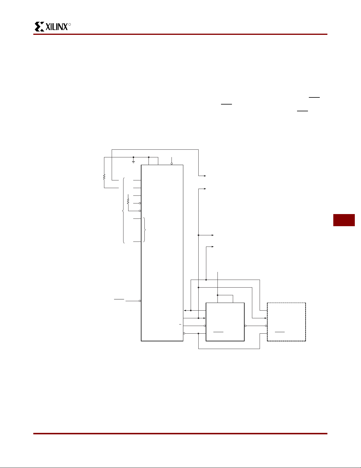
XC3000-Series Field Programmable Gate Arrays (FPGAs)
provide a group of high-performance, high-density, digital
integrated circuits. Their regular, extendable, flexible,
user-programmable array architecture is composed of a
configuration program store plus three types of configurable elements: a pe rimeter of I/O Blocks (IO Bs), a core
array of Configurable Logic Bocks (CLBs) and resources
for interconnection. The general structure of an FPGA is
shown in Figure 2. The development system provides
schematic capture and auto place-and-route for design
entry. Logic and timing simulation, and in-circuit emulation
are availabl e as desig n verifi cation alternat ives. Th e design
editor is used for interactive design optimization, and to
compile the data pattern that represents the configuration
program.
The FPGA user logic functions and interconnections are
determined by the configuration program data stored in
internal static memory cells. The program can be loaded in
any of several modes to accommodate various system
requirements. The program data resides externally in an
EEPROM, EPROM or ROM on the application circuit
board, or on a flop py d isk o r har d di sk. O n-ch ip in itia liza tion
logic provides for optional automatic loading of program
data at power-up. The companion XC17XX Serial Configuration PROMs provide a very simple serial configuration
program storage in a one-time programmable package.
The XC3000 Field Prog ramm able Ga te Array familie s provide a variety of logic capacities, package styles, temperature ranges and speed grades.
XC3000 Series Overview
There are now four distinct family groupings within the
XC3000 Series of FPGA devices:
• XC3000A Family
• XC3000L Family
• XC3100A Family
• XC3100L Family
All four families share a common architecture, develop-
ment software, design and programming methodology, and
also common package pin-outs. An extensive Product
Description covers these co mmon aspects.
Detailed parametric information for the XC3000A,
XC3000L, XC3100A, and XC3100L product families is then
provided. (The XC300 0 and XC3100 families are not recommended for new designs.)
Here is a simple overview of those XC3000 products currently emphasized:
• XC3000A Family — The XC3000A is an enhanced
version of the basic XC3000 family, featuring additional
interconnect resources and other user-friendly
enhancements.
• XC3000L Family — The XC3000L is identical in
architecture and features to the XC3000A family, but
operates at a nom inal supply volta ge of 3.3 V. The
XC3000L is the right solution for battery-operated and
low-power applications.
• XC3100A Family — The XC3100A is a
performance-optimized relati ve of the XC3000A fami ly.
While both families are bitstream and footprint
compatible, the XC 3100A fa mily ex tends t oggle rates to
370 MHz and in-system performance to over 80 MHz.
The XC3100A family also offers one additional array
size, the XC3195A.
• XC3100L Family — The XC3100L is identical in
architectures and features to the XC3100A family, but
operates at a nom inal supply voltage of 3.3V.
Figure 1 illustrates the relationships betw een the families.
Compared to the original XC3000 family, XC3000A offers
additional fu nctiona lity and increas ed speed. The XC3000 L
family offers the same additional functionality, but reduced
speed due to its lower supply voltage of 3.3 V. The
XC3100A family offers substantially higher speed and
higher density with the XC3195A.
New XC3000 Series Compared to Original
XC3000 Family
For readers already familiar with the original XC3000 family
of FPGAs, the major new features in the XC3000A,
XC3000L, XC3100A, and XC3100L families are listed in
this section.
All of these new families are upward-compatible extensions
of the original XC3000 FPGA architecture. Any bitstream
used to configure an XC 30 00 d evic e will co nfig ur e th e co r responding XC3000A, XC3000L, XC3100A, or XC3100L
device exactly the same way.
The XC3100A and XC3100L FPGA architectures are
upward-compatible extensions of the XC3000A and
XC3000L architec tures . Any bits tream used to conf igure an
XC3000A or XC3000L device will configure the corresponding XC3100A or XC3100L device exactly the same
way.
7-4 November 9, 1998 (Version 3.1)
Page 3

R
Improvements in the XC3000A and XC3000L
Families
The XC3000A and XC3000L families offer the following
enhancements over the popular XC3000 family:
The XC3000A and XC3000L families have additional interconnect resources to drive the I-inputs of TBUFs driving
horizontal Longlines. The CLB Clock Enable input can be
driven from a secon d vert ical Lon glin e. These two ad dition s
result in more efficient and faster designs when horizontal
Longlines are used for data bussing.
During configuration, the XC3000A and XC3000L devices
check the bit-stream format for stop bits in the appropriate
positions. Any error terminates the configuration and pulls
INIT Low.
When the configuration process is finished and the device
starts up in user mode , the first ac tivation of the outputs is
automatically slew-rate limited. This feature, called Soft
Startup, avoids the potential ground bounce when all
out-puts are turn ed on simultaneously. After start-up, the
slew rate of the indi vidual outputs i s, as in the XC 3000 family, determined by the individu al configuration option.
XC3000 Series Field Programmable Gate Arrays
Functionality
XC3100A
XC3100L
XC3100
XC3000A
XC3000L
Speed
(XC3195A)
Gate Capacity
X7068
Figure 1: XC3000 FPGA Families
Improvements in the XC3100A and XC3100L
Families
Based on a more advanced CMOS process, the XC3100A
and XC3100L families are architecturally- identical, performance-optimized relatives of the XC3000A and XC3000L
families. While all families are footprint compatible, the
XC3100A family extends achievable system performance
beyond 85 MHz.
7
November 9, 1998 (Version 3.1) 7-5
Page 4
XC3000 Series Field Programmable Gate Arrays
Detailed Functional Description
The perimeter of configurable Input/Output Blocks (IOBs)
provides a programmable interface between the internal
logic array and the device package pins. The array of Configurable Log ic Bloc ks (CLBs ) perfo rms user- specif ied log ic
functions. The interconnect resources are programmed to
form networks, carrying logic signals among blocks, analogous to printed circuit board traces connecting MSI/SSI
packages.
The block logic functions are implemented by programmed
look-up table s. Fu nc t iona l op tio ns ar e imp l eme nted b y pro gram-controlled multiplexers. Interconnecting networks
between blocks are implemented with metal segments
joined by program-controlled pass transistors.
These FPGA functions are established by a configuration
program which is loaded into an internal, distributed array
of configuration memory cells. The configuration program
is loaded into the device at power-up and may be reloaded
on command. Th e FPGA includes logic and control signals
to implement automatic or passive configuration. Program
R
data may be either bit serial or byte parallel. The development system generates the configuration program bitstream used to configure the device. The memory loading
process is independent of the user logic functions.
Configuration Memory
The static mem ory cell used for the config uration m emory
in the Field Programmable Gate Array has been designed
specifically for high reliability and n oise immunit y. Integrity
of the device con fi g urat i on me mor y bas ed o n th i s des i gn is
assured even under adverse conditions. As shown in
Figure 3, the basic memory cell consists of two CMOS
inverters pl us a p ass tr ansi stor used for w riti ng a nd rea ding
cell data. The cell is only written during configu ration and
only read during readback. During normal operation, the
cell provides continuous control and the pass transistor is
off and does not affect cell stability. This is quite different
from the operation of conventional memory devices, in
which the cell s are frequently re ad and rewritten.
DN
P11
TCL
KIN
P12
P13
U61
I/O Blocks
P9 P8 P7 P6 P5 P4 P3 P2 GNDPWR
3-State Buffers With Access
to Horizontal Long Lines
Interconnect Area
BBBA
Configurable Logic
Blocks
Frame Pointer
Configuration Memory
ADACABAA
X3241
Figure 2: Field Programmable Gate Array Structure.
It consists of a perimeter of programmable I/O blocks, a core of config urable logic blocks and their interconnect resources.
These are all controlled by the distributed array of configuration program memory cells.
7-6 November 9, 1998 (Version 3.1)
Page 5
R
Figure 3: Static Configuration Memory Cell.
It is loaded with one bit of configuration program and controls one program selection in the Field Programmable
Gate Array.
Q
Configuration
Control
Read or
Q
Write
Data
X5382
The memory cell outpu ts Q and Q use groun d and VCC levels and provide continuous, direct control. The additional
capacitive load together with the absence of address
decoding and sen se amp lifiers provid e high st ability to the
cell. Due to the structure of the configuration memory cells,
they are not affected by extreme power-supply excursions
or very high levels of alpha particle rad iation. In reliability
XC3000 Series Field Programmable Gate Arrays
testing, no soft errors have been observed even in the
presence of very high doses of alpha radiation.
The method of loading the configuration data is selectable.
Two methods use serial data, while three use byte-wide
data. The intern al configu ration log ic utilizes framin g infor mation, embedded i n the p rogram d ata by the developme nt
system, to direct memory-cell loading. The serial-data
framing and length-count preamble provide programming
compatibility for mixes of various FPGA device devices in a
synchronous, serial, daisy-chain fashion.
I/O Block
Each user-conf igurabl e IOB show n in Figur e 4, prov ides an
interface between the external package pin of the device
and the internal user logic. Each IOB includes both registered and dir ect in put paths. Each I OB pro vides a pr ogrammable 3-state output buffer, which may be driven by a
registered or direct output signal. Configuration options
allow each IOB an inversion, a controlled slew rate and a
high impedance pull-up. Each input circuit also provides
input clamping diodes to provide electrostatic protection,
and circuits to inhibit latch-up produced by input currents.
Vcc
I/O PAD
CK1
CK2
X3029
(OUTPUT ENABLE)
3- STATE
DIRECT IN
REGISTERED IN
OUT
PROGRAM
CONTROLLED
MULTIPLEXER
T
O
I
Q
OUT
INVERT
PROGRAM-CONTROLLED MEMORY CELLS
3-STATE
INVERT
FLIP
FLOP
R
FLIP
FLOP
or
LATCH
R
IKOK
=
PROGRAMMABLE INTERCONNECTION POINT or PIP
OUTPUT
SELECT
QD
DQ
TTL or
CMOS
INPUT
THRESHOLD
SLEW
RATE
OUTPUT
BUFFER
PASSIVE
PULL UP
(GLOBAL RESET)
Figure 4: Input/Output Block.
Each IOB includes input and output storage elements and I/O options selected by configuration memory cells. A choice
of two clocks is available on each die edge. The polarity of each clock line (not each flip-flop or latch) is programmable.
A clock line that triggers the fl ip-flop on the rising edge is an active Low Latch Enable (Latch transparent) signal and vic e
versa. Passive pull-up can only be enabled on inputs, not on outputs. All user inputs are programmed for TTL or CMOS
thresholds.
7
November 9, 1998 (Version 3.1) 7-7
Page 6

XC3000 Series Field Programmable Gate Arrays
R
The input-buffer portion of each IOB provides threshold
detection to translate external signals applied to the package pin to internal logic levels. The global input-buffer
threshold of th e IOBs can be programme d to be compa tible
with either TTL or CMOS lev els. The buffer ed input sign al
drives the data input of a storage element, which may be
configured as either a flip-flop or a latch. The clocking
polarity (rising/falling edge-triggered flip-flop, High/Low
transparent latch) is programmable for each of the two
clock lines on each of the four die edges. Note that a clock
line driving a
rising
edge-triggered f l ip- fl op mak es a ny l a tch
driven by the same line on the same edge Low-level trans-
falling
edge,
High
parent and vice ve rsa (
transparent). All
Xilinx primitives in the supported schematic-entry packages, however, are positive edge-triggered flip-flops or
High transparent latches. When one clock line m ust drive
flip-flops as well as latch es, it is nec essary t o compensa te
for the difference in clocking polarities with an additional
inverter either in the flip-flop clock input or the latch-enable
input. I/O storage elements are reset during configuration
or by the active-Low chip RESET
input. Both direct inp ut
(from IOB pi n I) a nd regi stered input (from IOB p in Q) s ignals are available for interconnect.
For reliable operation, inputs should have transition times
of less than 100 ns and should not be left floati ng. Floating
CMOS input-pin circuits might be at threshold and produce
oscillations. This can p roduce a dditional pow er dissip ation
and system noise. A typical hysteresis of about 300 mV
reduces sensitivity to input noise. Each user IOB includes a
programmable high-impedance pul l-up resistor, which may
be selected by the program to prov ide a cons tant High for
otherwise undriven package pins. Although the Field Programmable Gate Array provides circuitry to provide input
protection for electrostatic discharge, normal CMOS handling precautions should be observed.
Flip-flop loop delay s for the IOB and logic-bloc k flip-flops
are short, providing good performance under asynchronous clock and dat a conditi ons. Shor t loop del ays mini mize
the probability of a metastable condition that can result
from assertion of the clock during data transitions. Because
of the short-loop -de lay charac terist ic in th e Fie ld Pr ogr ammable Gate Ar ray, the IOB flip-flops can be used to synchronize external signals applied to the device. Once
synchronized in the IOB, the signals can be used internal ly
without further consideration of their clock relative timing,
except as it applies to the internal logic and routing-path
delays.
IOB output buffers provide CMOS-compatible 4-mA
source-or-sink drive for high fan-out CMOS or TTL- compatible signal levels (8 mA in the XC3100A family ). The network driving IOB pin O becomes the registered or direct
data source for the output buffer. The 3-state control signal
(IOB) pin T can control output activity. An open-drain output
may be obtained by using the same signal for driving the
output and 3-state signal nets so that the buffer output is
enabled only for a Low.
Configuration program bits for each IOB control features
such as optional output register, logic signal inversion, and
3-state and slew-rate control of the output.
The program-controlled memory cells of Figure 4 control
the following options.
• Logic inversion of the output is controlled by one
configuration program bit per IOB.
• Logic 3-state control of each IOB output buffer is
determined by the states of configuration program bits
that turn the buffer on, or off, or select the output buffer
3-state cont rol interconnection (IOB pin T). When this
IOB output con tr ol s i gn al i s Hi g h, a l og ic o ne, t he buffer
is disabled and the package pin is high impedance.
When this IOB outp ut contr ol signa l is Low, a logic ze ro,
the buffer is enabled and the package pin is active.
Inversion of the buffer 3-state control-logic sense
(output enable) is controlled by an additional
configuration program bit.
• Direct or registered output is selectable for each IOB.
The register uses a posit ive-e dge, clo cked f lip- flo p. The
clock source may be supplied (IOB pin OK) by either of
two metal lines available along each die edge. Each of
these lines is driven by an invertible buffer.
• Increased output transition speed can be selecte d to
improve cri tical timing. Slower transiti ons reduce
capacitive-load peak currents of non-criti cal outputs
and minimize system noise.
• An internal high-impedance pull-up resistor (active by
default) prevents unconnected inputs from floating.
Unlike the original XC3000 series, the XC3000A,
XC3000L, XC3100A, and XC3100L families include the
Soft Startup feature. When the configuration process is finished and the device starts up in user mode, the first activation of the o utputs is automa tically slew-rate lim ited. This
feature avoids potential ground bounce when all outputs
are turned on si multaneously. After start-up, the sle w rate
of the individual outputs is determined by the individual
configuration option.
Summary of I/O Options
• Inputs
-Direct
- Flip-flop/latch
- CMOS/TTL threshold (chip inputs)
- Pull-up resistor/open circuit
• Outputs
- Direct/registered
- Inverted/not
- 3-state/on/off
- Full speed/slew limited
- 3-state/output enable (inverse)
7-8 November 9, 1998 (Version 3.1)
Page 7
R
XC3000 Series Field Programmable Gate Arrays
Configurable Logic Block
The array of CLBs provides the functional elements from
which the user’s logic is constructed. The logic blocks are
arranged in a matrix within the perimeter of IOBs. For
example, the XC3020A has 64 such blocks arranged in 8
rows and 8 colu mns. The deve lopment system is used to
compile the confi guration data which is to be loaded into
the internal configuration memory to define the operation
and interconnection of each block. User definition of CLBs
and their interconnecting networks may be done by automatic transla tion from a sche matic-c apture logi c diagram or
optionally by installing library or user macros.
Each CLB has a combina torial logic se ction, two flip -flops,
and an internal control section. See Figure 5. There are:
five logic inputs (A, B, C, D and E); a common clock input
(K); an asynchronous direct RESET input (RD); and an
enable clock (EC). All may be driven from the interconnect
DATA IN
LOGIC
VARIABLES
DI
QX
A
B
C
D
E
COMBINATORIAL
FUNCTION
QY
F
G
resources adjacent to the blocks. Each CLB also has two
outputs (X and Y) which may drive i nterconnect networks.
Data input for either flip -flop within a CLB is su pplied from
the function F or G outp uts of th e combin atorial logic, or the
block input, DI. Both flip-flops in each CLB share the asynchronous RD which, when enabled and High, is dominant
over clocked inputs. All flip-flops are reset by the
active-Low chip input, RESET
, or during the configuration
process. The flip-flops share the enable clock (EC) which,
when Low, recirculates the flip-flops’ present states and
inhibits response to the data-in or combinatorial function
inputs on a CLB. The user may enable these control inputs
and select their sources. The user may also select the
clock net input (K), as well as its active sense within each
CLB. This programmable inversion eliminates the need to
route both phases of a clock signal throughout the device.
0
F
DIN
G
F
DIN
G
MUX
1
0
MUX
1
Q
D
RD
QD
QX
F
G
QY
X
CLB OUTPUTS
Y
7
ENABLE CLOCK
CLOCK
DIRECT
RESET
EC
1 (ENABLE)
K
RD
0 (INHIBIT)
(GLOBAL RESET)
RD
X3032
Figure 5: Configurable Logic Block.
Each CLB includes a co m bi nato ria l logic section, two flip-flo ps an d a p rogr am me m o ry co nt ro lled mu ltip lex er se lectio n of
function. It has the following:
- five logic variable inputs A, B, C, D, and E
- a direct data in DI
- an enable clock E C
- a clock (invertible) K
- an asynchronous direct RESET RD
- two outputs X and Y
November 9, 1998 (Version 3.1) 7-9
Page 8
XC3000 Series Field Programmable Gate Arrays
Flexible routing allows use of common or individual CLB
clocking.
The combinatorial-logic portion of the CLB uses a 32 by 1
look-up table to implement Boolean functions. Variables
selected from the five logic inputs and two internal block
flip-flops are used as ta ble address inputs. The combinatorial propagation delay through the network is independent
of the logic funct ion generated and is spike fre e for single
input variable changes. This technique can generate two
independent logic functions of up to four variables each as
shown in Figure 6a, or a single function of five variab les as
shown in Figure 6b , or some function s of seven variab les
as shown in Figu re 6c. Figure 7 shows a modulo-8 binary
counter with paralle l en abl e. It us es one CL B of ea ch typ e.
The partial functio ns of six or seven variables are implemented using the input variable (E) to dynamically select
between two functions of four different variables. For the
two functions of four variables each, the independent
results (F and G) may be used as data inputs to either
flip-flop or either logic block output. For the single function
of five variables and merged functions of six or seven variables, the F and G out put s are ide nti cal. Symmetr y of t he F
and G functions and the flip-flops allows the interchange of
CLB outputs to optimiz e routing eff icienc ies of th e networ ks
interconnecting the CLBs and IOBs.
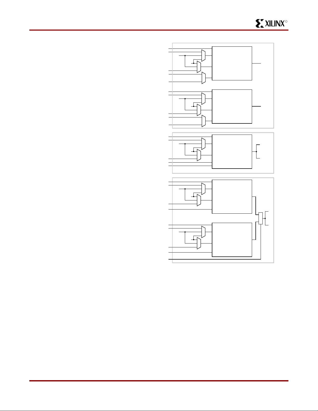
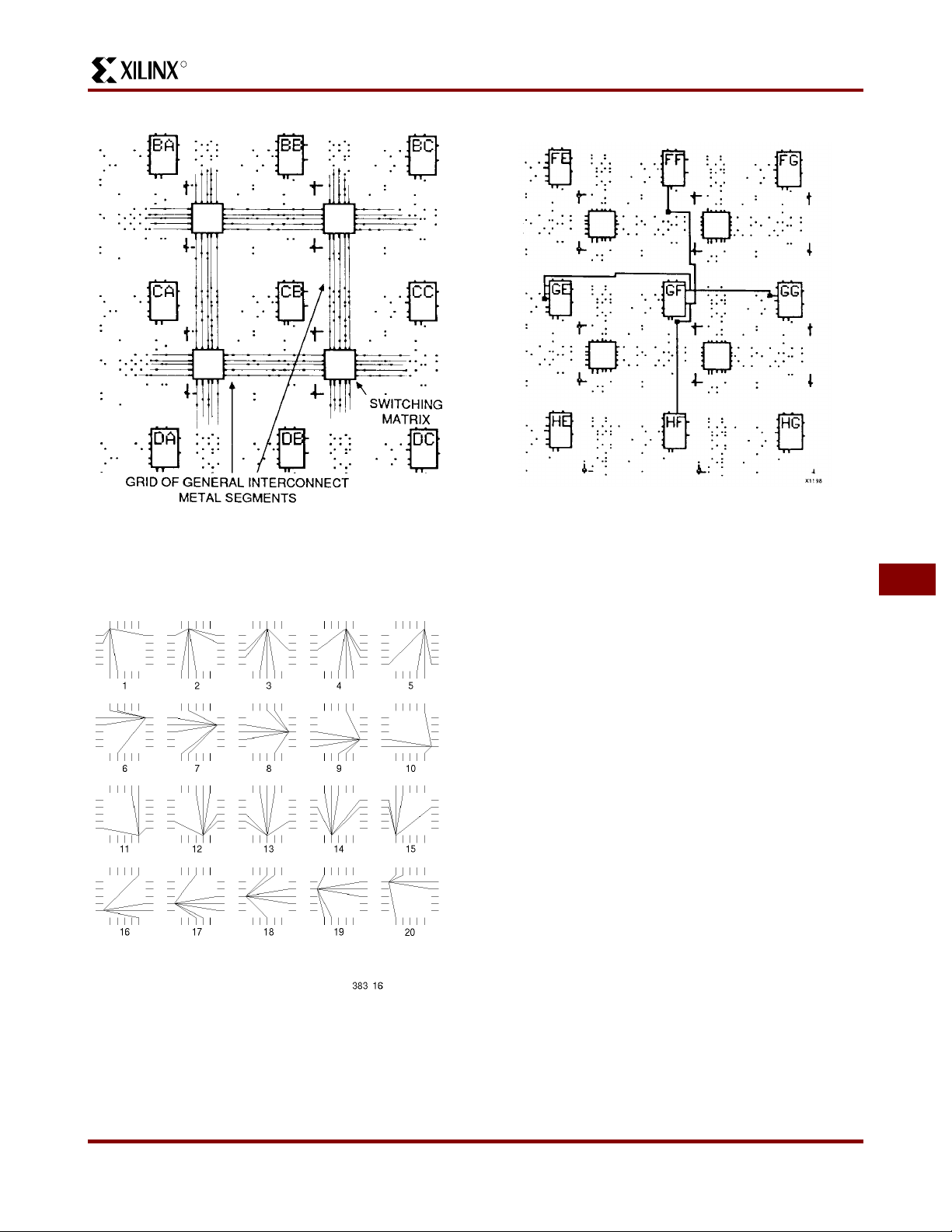
Programmable Interconnect
Programmable-interconnection resources in the Field Programmable Gate Array provide routing paths to connect
inputs and outputs of the IOBs and CLBs into logic networks. Inter connect ions between b locks are com posed o f a
two-layer grid of metal segments. Specially designed pass
transistors, each controlled by a configuration bit, form programmable interconnect points (PIPs) and switching matrices used to impl ement the n ecess ary connec tions be tween
selected metal segments and block pins. Figure 8 is an
example of a routed ne t. The develop ment system pr ovides
automatic routing of these interconnections. Interactive
routing is al so available for d esign optimization. The inputs
of the CLBs or IOBs are multiplexers which can be programmed to select an input network from the adjacent
interconnect segments.
block inputs are unidirectional, as are block outputs,
they are usabl e only for block input connect ion and n ot
for routing.
Figure 9 illustrates routing access to logic
block input variables, control inputs and block outputs.
Three types of met al reso urce s ar e pr ovide d to acco mmodate various network interconnect requirements.
• General Purpose Interconnect
• Direct Connection
• Longlines (multiplexed busses and wide AND gates)
Since the switch connections to
A
B
QX
QY
C
D
E
A
B
QX
QY
C
D
E
A
B
QX
QY
C
D
E
A
B
QX
QY
C
D
A
B
QX
QY
C
D
E
Any Function
of Up to 4
Variables
Any Function
of Up to 4
Variables
Any Function
of 5 Variables
Any Function
of Up to 4
Variables
Any Function
of Up to 4
Variables
F
G
5a
F
G
5b
F
M
U
X
G
FGM
5c
Mode
X5442
Figure 6: Combinationa l Logic Options
6a. Combinatorial Logic Option FG generates two func-
tions of four variables each. One variable, A, must be
common to bot h func t i ons. Th e se cond a nd t hir d v ar i ab le
can be any choice of B, C, QX and QY. The fourth variable can be any choice of D or E.
6b. Combinatorial Logic Option F generates any function
of five vari ables : A, D, E and two choi ces o ut of B, C, QX,
QY.
6c. Combinatorial Logic Option FGM allows variable E to
select betwee n tw o fun ction s of four vari ables : Bot h hav e
common inputs A and D and any choice out of B, C, QX
and QY for the remaining two variables. Option 3 can
then implemen t som e f unc t ion s o f s i x or se ve n v ar i able s.
R
7-10 November 9, 1998 (Version 3.1)
Page 9
R
Figure 7: Counter.
The modulo-8 binary counter with parallel enable and
clock enable uses one combinatorial logic block of each
option.
XC3000 Series Field Programmable Gate Arrays
Count Enable
Parallel Enable
Clock
Dual Function of 4 Variables
D0
D1
Function of 5 Variables
D2
Function of 6 Variables
D Q
D Q
D Q
Terminal
Count
Q0
FG
Mode
Q1
F
Mode
Q2
FGM
Mode
X5383
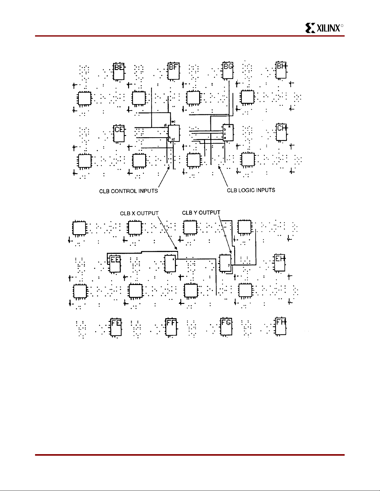
General Purpose Interconnect
General purpo se int er c onn ect, a s s ho wn i n Fig ur e 10 , con sists of a grid of five horizontal and five vertical metal segments located between the rows and columns of logic and
IOBs. Each segment is the height or width of a logic block.
Switching matrices join the ends of these segments and
allow progra mmed inte rconnect ions b etween t he meta l grid
segments of ad joining ro ws and co lumns. T he swit ches of
an unprogrammed device are all non-conducting. The connections through the switch matrix may be established by
the automatic routing or by selecting the desired pairs of
matrix pins to be connected or disconnected. The legitimate switching matrix combinations for each pin are indicated in Figure 11.
Special buffers within th e general intercon nect areas provide periodic signal isolation and restoration for improved
performance of lengthy nets. The interconnect buffers are
available to pro pagat e s ign al s in ei ther di re cti o n on a giv en
general interconnect segment. These bidirectional (bidi)
buffers a re fou nd adj acent to the switc hing ma tri ces, ab ove
Figure 8: A Design Editor vi ew of rout ing reso urces
used to form a typical interconnection network from
CLB GA.
and to the right. The other PIPs adjacent to the matrices
are accessed to or from Longlines. The development system automatically defines the buffer direction based on the
location of the inte rconnection networ k source. The delay
calculator of the development system automatically calculates and dis pla ys the blo ck, i nte rcon nect a nd buf f er d ela ys
for any paths selected. Generation of the simulation netlist
with a worst-case delay model is provided.
Direct Interconnect
Direct interconn ect, sh own in Figure 12, provides the most
efficient implementation of networks between adjacent
CLBs or I/O Blocks. Signals routed from block to block
using the dir ect in terc onne ct ex hibit mini mum int erconn ect
propagation and use no general interconnect resources.
For each CLB, the X output may be connected directly to
the B input of the CLB immediately to its right and to the C
input of th e CLB to its l eft. The Y out put ca n use di rect i nterconnect to driv e the D input of t he bloc k immed iat ely abo ve
and the A input of the block below. Direct interconnect
should be used to maxi mize the speed of high-perf ormance
portions of logic. Where logic blocks are adjacent to IOBs,
direct connect is provided alternately to the IOB inputs (I)
and outputs (O) on all four edges of the die. The right edge
provides additional direct connects from CLB outputs to
adjacent IOBs. Direc t interconnections of IOBs with CLBs
are shown in Figure 13.
7
November 9, 1998 (Version 3.1) 7-11
Page 10
XC3000 Series Field Programmable Gate Arrays
R
Figure 9: Design Edito r Loca tio ns of i nte rconnec t ac cess , CLB c ont rol i nputs, log ic i nputs and outp uts. Th e dot patt ern
represents th e available programmable interconnection points (PIPs).
Some of the interc onnect PIPs are directional.
7-12 November 9, 1998 (Version 3.1)
Page 11
R
Figure 10: FPGA General-Purpo se Interconnect.
Composed of a grid of metal segments that may be interconnected throug h switch matrices to form networks for
CLB and IOB inputs and outputs.
Figure 1 1: Swi tch Ma trix Int erconne ctio n Opti ons for
Each Pin.
Switch matrices on the edges are different.
XC3000 Series Field Programmable Gate Arrays
Figure 12: CLB X and Y Outputs.
The X and Y outputs of each CLB have single contact,
direct access to inputs of adjacent CLBs
7
November 9, 1998 (Version 3.1) 7-13
Page 12
XC3000 Series Field Programmable Gate Arrays
R
Global Buffer Direct Input
Global Buffer Inerconnect
* Unbonded IOBs (6 Places)
Figure 13: XC3020A Die-Edge IOBs. The XC3020A die-edge IOB s are provided with direct access to adjacent CLBs.
7-14 November 9, 1998 (Version 3.1)
Alternate Buffer Direct Input
Page 13
R
XC3000 Series Field Programmable Gate Arrays
Longlines
The Longlines bypass the swi tch mat rices and are intend ed
primarily for signals that must travel a long distance, or
must have minimum skew among multiple destinations.
Longlines, shown in Figure 14, run vertically and horizo ntally the heig ht or width of the interco nnect area . Each inter connection column has three vertical Longlines, and each
interconnection row has two horizontal Longlines. Two
additional Longlines are located adjacent to the outer sets
of switching matrices. In devices larger than the XC3020A
and XC3120A FPGAs , two vertical Longlines in ea ch col-
umn are connectable half-length lines. On the XC3020A
and XC3120A FPGAs, only the outer Longlines are connectable half-length lines.
Longlines can be dri ve n b y a l og ic blo ck or IOB o utpu t on a
column-by-column bas is. This capability provides a common low skew contro l or clock line within each colu mn of
logic blocks. Interconnections of these Longlines are
shown in Figure 15. Isolation buffers are provided at each
input to a Longline and are enabled automatically by the
development sy stem when a connection is made.
7
Figure 14: Horizontal and Vertical Longlines. These Longlines provide high fan-out, low-skew signal distribution in
each row and column. The global buffer in the upper left die corner drives a common line throughout the FPGA.
November 9, 1998 (Version 3.1) 7-15
Page 14
XC3000 Series Field Programmable Gate Arrays
R
Figure 15: Programmable Interconnection of Longlines. T h is is provided at the edges of the routing area.
Three-state b uf f er s al low t he use of ho riz on ta l Lo ng l ines t o fo rm on- chi p wir ed AND a nd mult ip le xe d b us es. The l eft t wo
non-clock vertical Longlines per column (except XC3020A) and the outer perimeter Longlines may be programmed as
connectable half-length lines.
VCC
Z
= DA • DB • DC • ... • DN
(LOW)
D
A
D
B
D
C
D
N
VCC
X3036
Figure 16: 3-State Buffers Implement a Wired-AND Function. When all the buffer 3-state lines are High, (high
impedance), the pull-up resistor(s) provide the High output. The buffer inputs are dr iven by the control signals or a Low.
WEAK
KEEPER CIRCUIT
DAA•+=D
D
A
A
D
B
B
B•+DCC•+ DNN•Z…+
B
D
C
C
D
N
N
X1741A
Figure 17: 3-State Buffers Implement a Multiplexer. The selection is ac complished by the buffer 3-state signal.
7-16 November 9, 1998 (Version 3.1)
Page 15
R
XC3000 Series Field Programmable Gate Arrays
A buffer in the upper left corner of the FPGA chip drives a
global net which is av ailable to all K inputs of logic bloc ks.
Using the global buffer for a clock signal provides a
skew-free, high fan-out, synchronized clock for use at any
or all of the IOBs and CLBs. Configuration bits for the K
input to each logic block can select this global line or
another routing resource as the clock source for its
flip-flops. This net may also be pr ogrammed to drive the die
edge clock lines for IOB use. An enhanced speed, CMOS
threshold, di rect acces s to thi s buffer is avail able at the s econd pad from the top of the left die edg e.
A buffer in the lower right corner of the array drives a horizontal Longline that can drive programmed connections to
a vertical Longline in each interconnection column. This
alternate buffer also has low skew and high fan-out. The
network formed by this alternate buffer’s Longlines can be
selected to drive th e K inputs of the CLBs. CMOS t hreshold, high speed access to this buffer is available from the
third pad from the bottom of the right die edge.
Internal Busses
A pair of 3- state buf fer s, lo cated a djacent to each CLB, permits logic to drive the horizontal Longlines. Logic operation
BIDIRECTIONAL
INTERCONNECT
BUFFERS
GG
GLOBAL NET
GH
of the 3-stat e buf fer c ontrols allows them t o implem ent wid e
multiplexing functions. Any 3-state buffer input can be
selected as drive for the horizontal long-line bus by applying a Low logic level on its 3-state control line. See
Figure 16. The user is required to avoid contention which
can result from multiple driv ers with op posing logic levels.
Control of the 3-state input by the same signal that drives
the buffer input , cr eate s an open -drai n wi red-AN D func tio n.
A logic High on both buffer inputs creates a high impedance, which rep res en t s n o co nten ti o n. A l ogic Lo w e nab les
the buffer t o dr iv e t he Lon gl in e Lo w. See Fig ur e 17 . Pull-up
resistors are available at each end of the Longline to provide a High output when all connected buffers are non-conducting. This forms fast, wide gating functions. When data
drives the inputs, and separate signals drive the 3-state
control lines, these buffers form multiplexers (3-state busses). In this case, care must be used to prevent contention
through multiple active buffers of conflicting levels on a
common line. Each horizontal Longline is also driven by a
weak keeper circuit that prevents undefined floating levels
by maintaining the p revio us log ic level wh en th e line is not
driven by an active buffer or a pull-up resistor. Figure18
shows 3-state buffers, Longlines and pull-up resistors.
3 VERTICAL LONG
LINES PER COLUMN
I/O CLOCKS
P48
HORIZONTAL LONG LINE
PULL-UP RESISTOR
7
P47
BCL
HG
P40 P41 P42 P43 RST
HH
OS
C
KIN
P46
.l
.lk
.q
.ck
.Q
D
P
G
M
Figure 18: Design Editor.
An extra large view of possible interconnections in the lower right corner of the XC3020A.
HORIZONTAL LONG LINE
OSCILLATOR
AMPLIFIER OUTPUT
DIRECTINPUT OF P47
TO AUXILIARY BUFFER
CRYSTAL OSCILLATOR
BUFFER
3-STATE INPUT
3-STATE CONTROL
3-STATE BUFFER
ALTERNATE BUFFER
X1245
November 9, 1998 (Version 3.1) 7-17
Page 16
XC3000 Series Field Programmable Gate Arrays
R
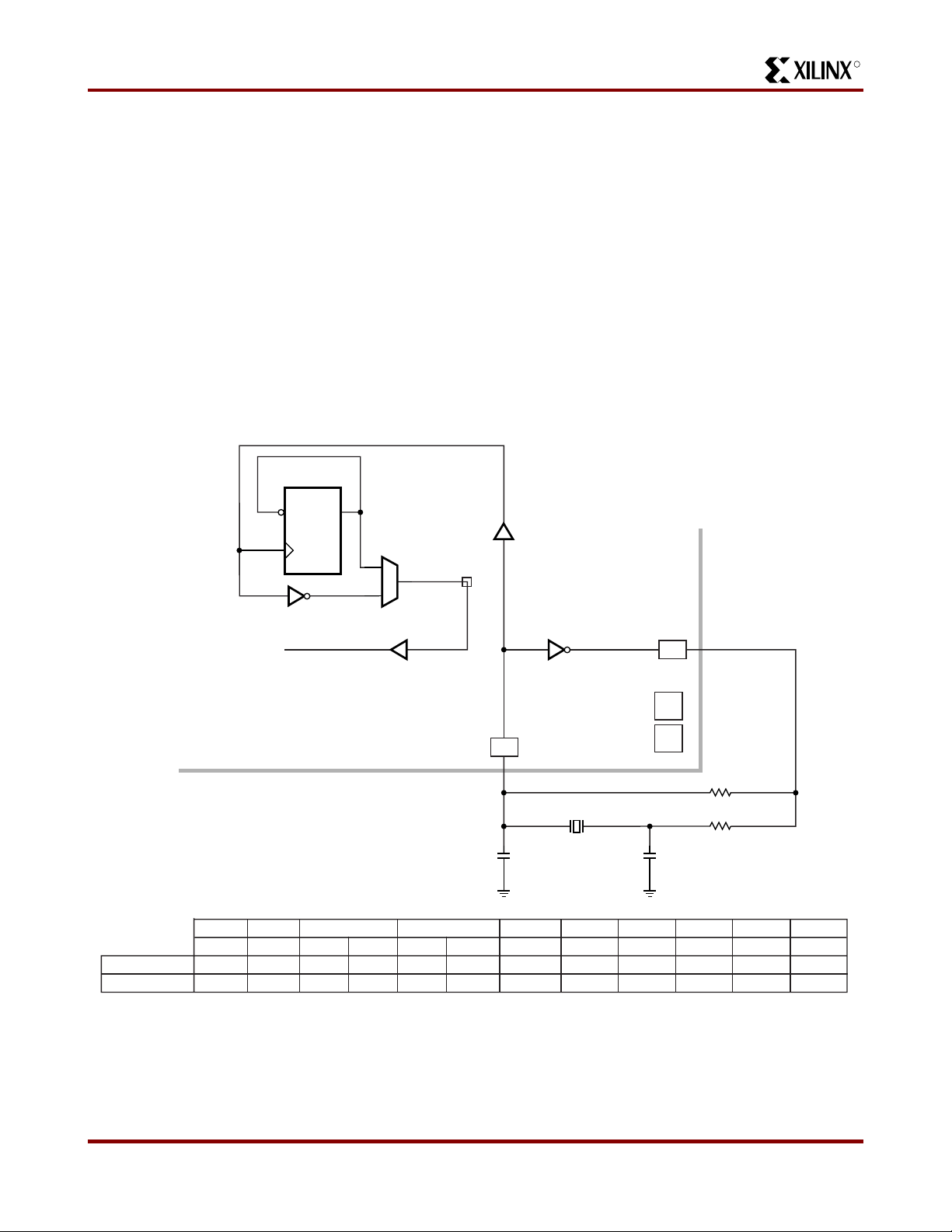
Crystal Oscillator
Figure 18 also sh ows th e l o ca tio n o f an in ter nal hi gh spe ed
inverting amplifier that may be used to implement an
on-chip crystal o scillator. It is associated with the au xiliary
buffer in the lower right corner of the die. When the oscillator is configured and connected as a signal source, two
special user IOBs are also configured to connect the oscillator amplifier w ith external crystal oscillator c omponents
as shown in Figure 19. A divide by two option is available to
assure symmetry. The oscillator circuit becomes active
early in the configu ration process to allow the oscillat or to
stabilize. Actual internal co nnection is delayed until completion of configuration. In Figure 19 the feedback resistor
R1, between the output and input, biases the amplifier at
threshold. The in version of th e amplifier, together with the
R-C networks and an AT-cut series resonant crystal, produce the 360-degre e phase s hift of the Pierce os cillator. A
D Q
series resistor R2 may be included to add to the amplifier
output impedance when needed for phase-shift control,
crystal resistance m atching, or to limit the amplifier input
swing to control clipping at large amplitudes. Excess feedback voltage may be corrected by the ratio of C2/C1. The
amplifier is designed to be used from 1 MHz to about
one-half the specified CLB toggle frequency. Use at frequencies below 1 MHz may require individual characterization with res pect to a ser ies resistance . Crystal osc illators
above 20 MHz general ly require a c rystal which oper ates in
a third overtone mode, where the fundamental frequency
must be suppressed by an inductor across C2, turning this
parallel resonant circuit to double the fundamental crystal
frequency, i.e., 2/3 of the desired third harmonic frequency
network. When the oscillator inverter is not used, these
IOBs and their package pins are available for general user
I/O.
Internal External
Suggested Component Values
R1
0.5 – 1 MΩ
R2
0 – 1 kΩ
(may be required for low frequency, phase
C1, C2
XTAL 1 (OUT)
XTAL 2 (IN)
shift and/or compensation level for crystal Q)
10 – 40 pF
Y1
1 – 20 MHz AT-cut parallel resonant
44 PIN
PLCC
30
26
68 PIN
PLCC
47
43
Alternate
Clock Buffer
84 PIN
PLCC
57
53
PGA
J11
L11
100 PIN
CQFP
67
61
XTAL2
(IN)
PQFP
82
76
Y1
C1 C2
132 PIN
PGA
160 PIN
PQFP
P13
M13
82
76
XTAL1
164 PIN
CQFP
105
99
R1
R2
175 PIN
PGA
T14
P15
176 PIN
TQFP
91
85
208 PIN
PQFP
110
100
X7064
Figure 19: Crystal Oscillator Inverter. When acti vated, and by selecting an output network for its bu ffer, the cryst a l
oscillator inverter uses two unconfigured package pins and external components to implement an oscillator. An optional
divide-by-two mode is available to assure symmetry.
7-18 November 9, 1998 (Version 3.1)
Page 17
R
XC3000 Series Field Programmable Gate Arrays
Configuration
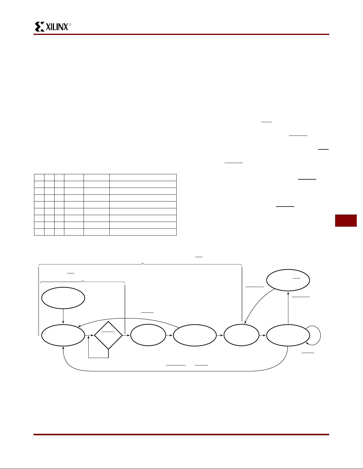
Initialization Phase
An internal power-on-reset circuit is triggered when power
is applied. Wh en V
of the FPGA device begin to operate (nominally 2.5 to 3 V),
the programmable I/O output buffers are 3-stated and a
high-impedance pull-up resistor is provided for the user
I/O pins. A time-out delay is initiated to allow the power
supply voltage to stabiliz e. During th is time the powe r-down
mode is inhibi t ed. Th e I n iti a li zati o n st at e t ime -o ut (abo ut 11
to 33 ms) is determined by a 14-bit counter driven by a
self-generated internal timer. This nominal 1-MHz timer is
subject to variations with process, temperature and power
supply. As shown in Table 1, five configuration mode
choices are available as determined by the input levels of
three mode pins; M0, M1 an d M 2.
Table 1: Configuration Mode Choices
M0 M1 M2 CCLK Mode Data
0 0 0 output Master Bit Serial
0 0 1 output Master Byte Wide Addr. = 0000 up
010— reserved —
0 1 1 output Mas te r Byte Wide Addr. = FFFF down
1 0 0 — reserved —
1 0 1 output Peripheral Byte Wide
1 1 0 — reserved —
1 1 1 i nput Slave Bit Serial
reaches the voltage at which portions
CC
In Master configuration modes, the device becomes the
source of the Configuration Clock (CCLK). The beginning
of configuration of devices using Peripheral or Slave
modes must be delayed long enough for their initialization
to be completed. An FPGA with mode lines selecting a
Master configuration mode extends its initialization state
using four times the delay (43 to 130 ms) to assure that all
daisy-chained slave devices, which it may b e driving, will
be ready even if the master is very fast, and the slave(s)
very slow . Figu re 20 shows the state sequ ences. At th e end
of Initialization, the device enters the Clear state where it
clears the configuration memory. The active Low,
open-drain initialization signal INIT
indicates when the Initialization and Clear states are complete. The FPGA tests
for the absence of an external active Low RESET
before it
makes a final sample of the mode lines and enters the Configuration s tat e. An ext erna l wir ed- AND of one or more INIT
pins can be used to co ntrol confi guration by the asserti on of
the active-Low RESET
of a master mode device or to sig-
nal a processor that the FPG A s ar e no t yet initia lized .
If a configuration has begun, a re-assertion of RESET
for a
minimum of three in ternal timer cycles will be r ecognized
and the FPGA will initiate an ab ort, returning to the Clear
state to clear the partially loaded configuration memory
words. The FPGA will then resample RESET
and the mode
lines before re-ent er in g the C on fig ur at ion stat e.
During configuration, the XC3000A, XC3000L, XC3100A,
and XC3100L devices check the bit-stream format for stop
bits in the appropr iate positions. Any erro r terminates the
configuration and pulls INIT Low.
7
All User I/O Pins 3-Stated with High Impedance Pull-Up, HDC=High, LDC=Low
INIT Output = Low
Initialization
Power-On
Time Delay
Clear
Configuration
Memory
Power-On Delay is
14
2
Cycles for Non-Master Mode—11 to 33 ms
16
2
Cycles for Master Mode—43 to 130 ms
RESET
Active
Active RESET
Test
Mode Pins
No
Low on DONE/PROGRAM and RESET
Configuration
Program Mode
Clear Is
~ 200 Cycles for the XC3020A—130 to 400 µs
~ 250 Cycles for the XC3030A—165 to 500 µs
~ 290 Cycles for the XC3042A—195 to 580 µs
~ 330 Cycles for the XC3064A—220 to 660 µs
~ 375 Cycles for the XC3090A—250 to 750 µs
PWRDWN
Inactive
Start-Up
Figure 20: A State Diagram of the Configuration Process for Power-up and Reprogram.
Power Down
No HDC, LDC
or Pull-Up
PWRDWN
Active
Operational
Mode
Active RESET
Operates on
User Logic
X3399
November 9, 1998 (Version 3.1) 7-19
Page 18
XC3000 Series Field Programmable Gate Arrays
R
A re-program is initiated.when a configured XC3000 series
device senses a Hig h- to -L ow trans i t ion a nd s ub seque nt >6
µs Low level on the DONE/PROG
package p in, or, if this
pin is externa ll y hel d p er man entl y Low, a High-to-Low transition and subse quent >6 µs Low time on the RESET
pack-
age pin.
The device returns to the Clear state where the configura-
tion memory is cleared and mode lines re-sampled, as for
an aborted configuration. The complete configuration program is cleared and loaded during each configuration program cycle.
Length count cont ro l allo ws a syst em of mu ltip le Fi el d Pr ogrammable Gate Arrays, of assorted size s, to begin operation in a synchronized fashion. The configuration program
11111111
0010
< 24-Bit Length Count >
1111
0 <Data Frame # 001 > 111
0 <Data Frame # 002 > 111
0 <Data Frame # 003 > 111
. . .
. . .
. . .
0 <Data Frame # 196 > 111
0 <Data Frame # 197 > 111
1111
*The LCA Device Require Four Dummy Bits Min; Software Generates Eight Dummy Bits
—Dummy Bits*
—Preamble Code
—Configuration Program Length
—Dummy Bits (4 Bits Minimum)
For XC3120
197 Configuration Data Frames
(Each Frame Consists of:
A Start Bit (0)
A 71-Bit Data Field
Three Stop Bits
Postamble Code (4 Bits Minimum)
generated by the development system begins with a prea mb le of 111111110 0 10 fo ll ow e d b y a 24 - bi t l en gt h co un t
representing the total number of configuration clocks
needed to complete loading of the configuration program(s). The data framing is shown in Figure 21. All
FPGAs connec ted in series read and shift preamble and
length count in on positive and o ut on negati ve configuration clock edges. A device which has received the preamble and length count then presents a High Data Out until it
has intercepted the appropriate number of data frames.
When the configuration program memory of an FPGA is full
and the length count does not yet compare, the device
shifts any additional data through, as it did for preamble
and length count. When the FPGA configuration memory is
full and the length coun t com pa re s, the de vice will ex ecute
Header
Program Data
Repeated for Each Logic
Cell Array in a Daisy Chain
X5300_01
XC3020A
Device
Gates 1,000 to 1,500 1,500 to 2,000 2,000 to 3,000 3,500 to 4,500 5,000 to 6,000 6,500 to 7,500
CLBs 64 100 144 224 320 484
Row x Col (8 x 8) (10 x 10) (12 x 12) (16 x 14) (20 x 16) (22 x 22)
IOBs 64 80 96 120 144 176
Flip-flops 256 360 480 688 928 1,320
Horizontal Longlines 16 20 24 32 40 44
TBUFs/Horizontal LL 9 11 13 15 17 23
Bits per Frame
(including1 start and 3 st op bits)
Frames 197 241 285 329 373 505
Program Data =
Bits x Frames + 4 bits
(excludes header)
PROM size (bits) =
Program Data
+ 40-bit Header
XC3020L
XC3120A
75 92 108 140 172 188
14,779 22,176 30,784 46,064 64,160 94,944
14,819 22,216 30,824 46,104 64,200 94,984
XC3030A
XC3030L
XC3130A
XC3042A
XC3042L
XC3142A
XC3142L
XC3064A
XC3064L
XC3164A
XC3090A
XC3090L
XC3190A
XC3190L XC3195A
Figure 21: Internal Configuration Data Structure for an FPGA. This shows the preamble, length count and data
frames generat ed by the Development Sy stem.
The Length Count produced by the program = [(40-bit preamble + sum of program data + 1 per daisy chain device)
rounded up to multiple of 8] – (2 ≤ K ≤ 4) where K is a function of DONE and RESET timing selected. An additional 8 is
added if roundup increment is less than K. K additional clocks are needed to complete start-up after length count is
reached.
7-20 November 9, 1998 (Version 3.1)
Page 19
R
XC3000 Series Field Programmable Gate Arrays
a synchronou s start -up s eque nce a nd become opera tio nal .
See Figure 22. Two CCLK cycles after the completion of
loading configuration data, the user I/O pins are enabled as
configured. As selected, the internal user-logic RESET is
released either one clock cycle before or after the I/O pins
become active. A sim ilar t iming selec tion is prog ramm able
for the DONE/PROG
output sig nal. DO NE/P ROG may also
be programmed to be an open drain or include a pull-u p
resistor to accom modate wired ANDing. T he High During
Configuration (HDC) and Low Durin g Configuration ( LDC
are two user I/O pins which are driven active while an
FPGA is in its Initialization, Clear or Configure states. They
and DONE/PROG
provide signals for control of external
logic signals such as RESET, bus enable or PROM enable
during configuration. For parallel Master configuration
modes, these signals provide PROM enable control and
allow the data pins to be shared with user logic signals.
User I/O inputs can be programmed to be either TTL or
CMOS compatible thresholds. At power-up, all inputs have
TTL thresholds and ca n change to CMOS t hres holds at the
completion of configuration if the user has selected CMOS
thresholds. The thr eshold of PWRDWN
and the direct cloc k
inputs are fixed at a CMOS level.
If the crystal oscillator is used, it will begin operation before
configuration is complete to allow time for stabilization
before it is connected to the internal circuitry.
12 24 4
Data Frame
Configuration Data
Configuration data to define the function and interconnection within a Field Programm able Gate Ar ray is load ed from
an external st orage at power-up and aft er a re- program si gnal. Several metho ds of automat ic and contr olled loadin g of
the required data are available. Logic levels applied to
mode selection pins at the start of configuration time determine the method t o be used . See Table 1. The dat a may be
either bit-serial or byte-parallel, depending on the configu-
)
ration mode. The different FPGAs have different sizes and
numbers of data frames. To maintain compatibility between
various device type s, the Xilinx product familie s use compatible configuration formats. For the XC3020A, configuration requires 14779 bits for each device, arranged in 197
data frames. An additional 40 bits are used in the header.
See Figure22. The specific data format for each device is
produced by the development system and o ne or more of
these files can then be comb ine d and appen ded t o a lengt h
count preamble and be transformed into a PROM format
file by the developmen t system. A compatibility excep tion
precludes the use of an XC2000-series device as the master for XC3000-series devices if their DONE or RESET are
programmed to occur after their outputs become active.
The Tie Option defines ou tput leve ls of un use d block s of a
design and connects these to unused routing resources.
This prevents indeterminate levels that might produce parasitic supply currents. If unused bloc ks are not suffici ent to
complete the tie, the user can indicate net s which must not
Last Frame
3
Postamble
3
STOP
4
7
DIN
Preamble Length Count Data
The configuration data consists of a composite
*
40-bit preamble/length count, followed by one or
more concatenated FPGA programs, separated by
4-bit postambles. An additional final postamble bit
is added for each slave device and the result rounded
up to a byte boundary. The length count is two less
than the number of resulting bits.
Timing of the assertion of DONE and
termination of the INTERNAL RESET
may each be programmed to occur
one cycle before or after the I/O outputs
become active.
Heavy lines indicate the default condition
Start
Bit
Stop
Start
Bit
Length Count*
Weak Pull-Up
PROGRAM
Internal Reset
I/O Active
DONE
X5988
Figure 22: Configurat ion and Start-up of One or More FPGAs.
November 9, 1998 (Version 3.1) 7-21
Page 20

XC3000 Series Field Programmable Gate Arrays
R
be used to drive the remaining unused routing, as that
might affect timing of user nets. Tie can be omitted for quick
breadboard iterat ions where a few additional millia mps of
Icc are acceptable.
The configuration bitstream begins with eight High preamble bits, a 4-bit preamble code and a 24-bit length count.
When configuration is initiated, a counter in the FPGA is set
to zero and begins to count the total number of configuration clock cycles ap plied to th e device . As each configur ation data frame is supplied to the device, it is internally
assembled into a data word, which is then loaded in parallel
into one word of th e internal configuration memory array.
The configuration loading process is complete when the
current le ngth cou nt equ als the load ed len gth coun t and the
required configuration program data frames have been
written. In tern al user f lip -flo ps a re he ld Re set during con fig uration.
Two user-programma ble pins are defined in th e unconfigured Field Progra mmab le Gate Ar ray. High During Configuration (HDC) and Low During Configuration (LDC
as DONE/PROG
during configuration. In Master mode configurations it is
convenient to use LDC
Enable. After the last configuration data bit is loaded and
the length count compares, the user I/O pins become
active. Options allow tim ing choices o f one clock e arlier or
later for the timing of the end of the internal logic RESET
and the assertion of the DONE signal. The open-drain
DONE/PROG
and used as an active -H igh REA DY, an active-Low PROM
enable or a RESET to other portions of the system. The
state diagram of Figure 20 illustrates the configuration process.
may be used as external control signals
as an active-Low EPROM Chip
output can be AND-tied with multiple devices
) as well
Configuration Modes
Master Mode
In Master mode, the FPGA automatically loads configuration data from an external memory device. There are three
Master modes that use the internal timing source to supply
the configuration clock (CCLK) to time the incoming data.
Master Serial mode uses serial configu r ation data supplied
to Data-in (DIN) from a synch ron ous se rial so urce such as
the Xilinx Serial Configurat ion PROM shown in Figure 23.
Master Parallel Low and High modes automatically use
parallel data supplied to the D0–D7 pins in response to the
16-bit address generated by the FPGA. Figure 25 shows
an example of the parallel Master mode connections
required. T he HEX s tarting addres s is 0 000 and increme nts
for Master Low mode and it is FFFF and decrements for
Master High mode. These two modes provide address
compatibility with microp rocessors which begin execution
from opposite ends of memory.
Peripheral Mode
Peripheral mode provides a simplified interface through
which the device may be loaded byte-wide, as a processor
peripheral. Figure 27 shows the peripheral mode connections. Processor write cycles are decoded from the common assertion of the active low Write Strobe (WS
active low and one active high Chip Selects (CS0
CS2). The FPGA generates a configuration clock from the
internal timing generator and serializes the parallel input
data for internal framing or for succeeding slaves on Data
Out (DOUT). A output High on READY/BUSY
the completion of loading for each byte when the input register is read y for a n ew byte. As with Master modes, P eripheral mode may also be used as a lead device for a
daisy-chain of slave devices.
), and two
, CS1,
pin indicates
Slave Serial Mode
Slave Serial mode provides a simple interface for loading
the Field Programmable Gate Array configuration as
shown in Figure29. Serial data is supplied in conjunction
with a synch ron izi n g inpu t c loc k. M ost S lav e m ode a ppli c ations are in daisy-chain configurations in which the data
input is driven from the p revi ous FP GA’s data out, whil e th e
clock is supplied by a lead device in Master or Peripheral
mode. Data may also be supplied by a processor or other
special circuits.
Daisy Chain
The development system is used to create a composite
configuration for selected FPGAs including: a preamble, a
length count for th e total bitstream, multiple concatena ted
data programs and a postamble plus an ad ditional fill bit
per device in the serial chain. After loading and passing-on
the preamble and length count to a possible daisy-chain, a
lead device will load its configuration data frames while providing a High DOUT to possible down-stream devices as
shown in Figure 25. Loading continues while the lead
device has received its configuration program and the current length count has not reached the full value. The additional data is passed through the lead device and appears
on the Data Out ( DOU T) p in i n s er ial f or m. T he le ad d ev i ce
also generates th e Conf igura tio n Clock (C CLK) t o sync hronize the serial output data and data in of down-stream
FPGAs. Data is r ead in on DIN of sla ve devi ces by the po sitive edge of CCLK and shifted out the DOUT on the negative edge of CC LK. A p aralle l M as te r mo de d ev ice use s its
internal timing generator to produce an internal CCLK of 8
times its EPROM address rate, while a Peripheral mode
device produc es a burst of 8 CCLKs for ea ch chip select
and write-strobe cycle. The internal timing generator continues to operate for general timing and synchronization of
inputs in all modes.
7-22 November 9, 1998 (Version 3.1)
Page 21
R
XC3000 Series Field Programmable Gate Arrays
Special Configuration Functions
The configuration data includes control over several special functions in addition to the normal user logic functions
and interconnect.
• Input thresholds
• Readback disabl e
• DONE pull-up resistor
•DONE timing
• RESET timing
• Oscillator frequen cy div ide d by two
Each of these functions is controlled by configuration data
bits which are selected as part of the normal development
system bitstream generation process.
Input Thresholds
Prior to the completion of configuration all FPGA input
thresholds a re TTL compatible. Upon completion of configuration, the input thresholds become either TTL or CMOS
compatible as programmed. The use of the TTL threshold
option requires some additional supply current for threshold shifting. The exception is the threshold of the
PWRDWN
CMOS input. Prior to the completion of configuration the
user I/O pins each have a high impedance pull-up. The
configuration program can be used to enable the IOB
pull-up resi stors in t he Op erat ional mode to a ct ei ther a s an
input load or to avoid a floating input on an otherwise
unused pin.
Readback
The contents of a Fi eld Progr amm able Gat e Arr ay ma y be
read back if it has been programmed with a bitstream in
which the Readback option has been enabled. Readback
may be used for verification of configuration and as a
method of deter mining the st ate of inte rnal logic nodes during debugging. There are three options in generating the
configuration bitstr ea m .
• “Never” inhibits the Read ba ck capa bility.
• “One-time, ” inhibits Readba ck after one Readback has
been executed to verify the configuration.
• “On-command ” allo ws unr es tric te d us e of Re ad ba ck .
Readback is ac complished without the use of any of the
user I/O pins; only M0, M1 and CCLK are used. The initiation of Readb ac k is pr odu c ed by a Lo w to Hi gh tr an sit i on o f
the M0/RTRIG (Read Trigger) pin. The CCLK input must
then be driven by ex t er nal l og ic t o re ad ba ck t he c onf ig ura tion data. The first three Low-to-High CCLK transitions
clock out dummy da ta. Th e subs equen t Low-t o-Hi gh CCLK
transitions shift the data frame information out on the
M1/RDATA
always inverted, a z ero in config uration be comes a one in
Readback, and vice ver sa. Note also that eac h Readback
frame has one Start bit (read back as a one) but, unlike in
input and direct clocks which always have a
(Read Data) pin. No te that the logic polarity is
configuration, each Readback frame has only one Stop bit
(read back as a zero). The third leading dummy bit mentioned above can be considered the Start bit of the first
frame. All data fr ames mus t be read ba ck to comp lete the
process and retu rn the Mode Sel ect and CCL K pins to thei r
normal functions.
Readback data includes the current state of each CLB
flip-flop, each input flip-flop or latch, and each device pad.
These data are imbedded into unused configuration bit
positions during Readback. This state information is used
by the development system In-Circuit Verifier to provide
visibility into the internal operation of the logic while the
system is operating. To readback a uniform time-sample of
all storage el ements , it may be nec essar y to in hibit the s ystem clock.
Reprogram
To initiate a re-programming cycle, the dual-function pin
DONE/PROG
reduce sensitivity to noise, the input signal is filtered for two
cycles of the FPGA internal timing generator. When reprogram begins, the us er-prog rammabl e I/O output buf fers are
disabled and high-impedance pull-ups are provided for the
package pins. The device returns to the Clear state and
clears the config uration memo ry before it ind icates ‘initialized’. Since this Cle ar operatio n uses chip-in dividual inte rnal timing, the master might co mplete the Clear operation
and then start co nfigurati on before th e slave has com pleted
the Clear operation. To avoid this problem, the slave INIT
pins must be AND-wired and used to force a RESET on the
master (see Figure 25). Reprogram control is often imple-
mented using an external open-collector driver which pulls
DONE/PROG
the DONE/PROG
tion has been co mple te d. Even i f t he r e- pro gr am requ es t i s
externally held Low beyond the configuration period, the
FPGA will begin oper ation upon completion of config uration.
must be given a High-to-Low transition. To
Low. Once a stable request is recognized,
pin is held Low until the new configura-
DONE Pull-up
DONE/PROG is an open-drain I/O pin that indicates the
FPGA is in the operational state. An optional internal
pull-up resistor can be enabled by the user of the development system. The DONE/PROG
a daisy-chain ma y be co nnect ed to geth er to i ndica te al l ar e
DONE or to direct them all to reprogram.
pins of multiple FPGAs in
DONE Timing
The timing of the DONE status signal can be controlled by
a selection to occur either a CCLK cycle before, or after, the
outputs going active. See Figure 22. This facilitates control
of external functions such as a PROM enable or holding a
system in a wait state.
7
November 9, 1998 (Version 3.1) 7-23
Page 22
XC3000 Series Field Programmable Gate Arrays
R
RESET Timing
As with DONE timing, the timing of the release of the internal reset can be controlled to occur either a CCLK cycle
before, or a fter, th e outputs going active. Se e Figure 22.
This reset keeps all user programmable flip-flops and
latches in a zero state durin g co nf igu ra tio n.
Crystal Oscillator Division
A selection allows the user to incorporate a dedicated
divide-by-two flip-flop between the crystal oscillator and the
alternate clock line. This guarantees a symmetrical clock
signal. Although t he freque ncy sta bility of a c rystal osc illator is very good, the symmetry of its waveform can be
affected by bias or feedback drive.
Bitstream Error Checking
Bitstream error checking pr otects agai nst erroneous con-
figuration.
Each Xilinx FPGA bitst ream consis ts of a 4 0-bit p reamble,
followed by a device-specific number of data frames. The
number of bits pe r frame is als o device-spe cific; however,
each frame ends with three stop bits (111) f ollowed by a
start bit for the next frame (0).
All devices in all XC3000 fam ilies start reading in a new
frame when the y find th e first 0 after the end of t he prev ious
frame. An original XC3000 device does not check for the
correct stop bits, but XC3000A, XC3100A, XC3000L, and
XC3100L devic es che ck that the last t hree bit s of any fra me
are actually 111 .
Under normal circumstances, all these FPGAs behave the
same way; however, if the bitstream is corrupted, an
XC3000 device will always start a n ew fram e as so on as it
finds the first 0 after the end of the previous frame, even if
the data is completely wrong or out-of-sync. Given sufficient zeros in the data stream, the device will also go Done,
but with incor rect config uration an d the po ssibility of inte rnal contention.
An XC3000A/XC3100A/XC3000L/XC3100L device starts
any new frame only if the three preceding bits are all ones.
If this check fails, it pulls INIT
configuration, although the Master CCLK keeps running.
The user must t hen start a new configuration by applying a
>6 µs Low level on RESET
This simple check does not protect against random bit
errors, but it offers almost 100 percent protection against
erroneous configuration files, defective configuration data
sources, synchronization errors between configuration
source and FPGA, or PC-board level defects, such as broken lines or solder-bridges.
Low and stops the int ernal
.
Reset Spike Protection
A separate modification slows down the RESET input
before configuration by using a two-stage shift register
driven from the in ternal cloc k. It tolerates s ubmicrose cond
High spikes on RESET
master can be connected like an XC4000 master, but with
its RESET
output only).
input used instead of INIT. (On XC3 000, INIT is
before config uration. The X C3000
Soft Start-up
After configuration, the outputs of all FPGAs in a
daisy-chain become active simultaneously, as a result of
the same CCLK edge. In the original XC3000/3100
devices, each output becomes active in either fast or
slew-rate limited mode, depending on the way it is configured. This can lead to large ground-bounce signals. In
XC3000A, XC3000L, XC3100A, and XC3100L devices, all
outputs become active first in slew-rate limited mode,
reducing the ground bounce. After this soft start-up, each
individual output slew rate is again controlled by the
respective configuration bit.
7-24 November 9, 1998 (Version 3.1)
Page 23
R
Configuration Timing
This section describes the configuration modes in detail.
Master Serial Mode
In Master Serial mode, the CCLK output of the lead FPGA
drives a Xilinx Serial PROM that feeds the DIN input. Each
rising edge of the CCLK output increments the Serial
PROM internal address counter. This puts the next data bit
on the SPROM data output, connected to the DIN pin. The
lead FPGA accepts this data on the subsequent rising
CCLK edge.
The lead FPGA then presents the preamble data (and all
data that over flows t he lead d evice) on its DOUT p in. There
is an internal delay of 1.5 CCLK periods, which means that
*
IF READBACK IS
ACTIVATED, A
5-kΩ RESISTOR IS
REQUIRED IN
SERIES WITH M1
DURING CONFIGURATION
THE 5 kΩ M2 PULL-DOWN
RESISTOR OVERCOMES THE
INTERNAL PULL-UP,
BUT IT ALLOWS M2 TO
BE USER I/O.
GENERAL-
PURPOSE
USER I/O
PINS
M0 M1 PWRDWN
DOUT
M2
+5V
HDC
LDC
INIT
•
•
•
OTHER
•
I/O PINS
•
*
XC3000
FPGA
DEVICE
+5 V
XC3000 Series Field Programmable Gate Arrays
DOUT changes on the falling CCLK edge, and the next
device in the daisy-chain accepts data on the subsequent
rising CCLK edge.
The SPROM CE input can be driven f rom either LDC
DONE. Using LDC
avoids potential contention on the DIN
pin, if this pin is configured as user-I/ O, but LDC
restricted to be a permanently High user output. Using
DONE also avoids contention on DIN, provided the early
DONE option is invoked.
TO DIN OF OPTIONAL
DAISY-CHAINED LCAs WITH
DIFFERENT CONFIGURATIONS
TO CCLK OF OPTIONAL
DAISY-CHAINED LCAs WITH
DIFFERENT CONFIGURATIONS
TO CCLK OF OPTIONAL
SLAVE LCAs WITH IDENTICAL
CONFIGURATIONS
TO DIN OF OPTIONAL
SLAVE LCAs WITH IDENTICAL
CONFIGURATIONS
or
is then
7
+5 V
RESET
RESET
V
DIN
CCLK
D/P
INIT
(LOW RESETS THE XC17xx ADDRESS POINTER)
CCVPP
DATA
CLK
CE
OE/RESET
SCP
XC17xx
CEO
DATA
CLK
CE
OE/RESET
CASCADED
SERIAL
MEMORY
X5989_01
Figure 23: Master Serial Mode C ircuit Diagram
November 9, 1998 (Version 3.1) 7-25
Page 24

XC3000 Series Field Programmable Gate Arrays
CCLK
(Output)
T
2
CKDS
T
DSCK
1
R
Serial Data In
Serial DOUT
(Output)
n – 3 n – 2 n – 1 n
n n + 1 n + 2
X3223
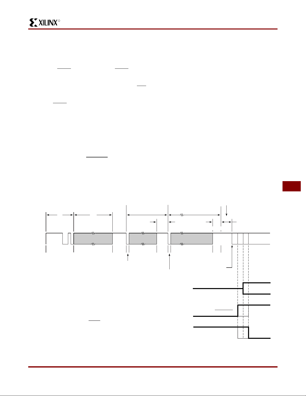
Description Symbol Min Max Units
CCLK
Data In setup 1 T
Data In hold 2 C
DSCK
KDS
Notes: 1. At power-up, VCC must rise from 2.0 V to VCC min in less than 25 ms. If this is not possible, configuration can be delayed by
holding RESET Low until V
non-monotonically rising V
after VCC has reached 4.0 V (2.5 V for the XC3000L).
2. Configuration can be controlled by holding RESET
has reached 4.0 V (2.5 V for the XC3000L). A very long VCC rise time of >100 ms, or a
CC
may require >6-µs Hig h le vel on RESET, f ol l owed by a >6-µs Low level on RESET and D/P
CC
Low with or until after the INIT of all daisy-chain slave-mode devices is
High.
3. Master-serial-mode timing is based on slave-mode testing.
60 ns
0ns
Figure 24: Master Serial Mode Programming Switching Characteristics
7-26 November 9, 1998 (Version 3.1)
Page 25

R
Master Parallel Mode
In Master Par all el mo de , the le ad FP GA di r ectl y ad dre sse s
an industry-standard byte-wide EPROM and accepts eight
data bits right before incrementing (or decrementing) the
address outputs.
The eight data bits are serialized in the lead FPGA, which
then presents the preamble data (and all data that overflows the lead device) on the DOUT pin. There is an inter-
XC3000 Series Field Programmable Gate Arrays
nal delay of 1.5 CCLK periods, after the rising CCLK edge
that accepts a byte of data, and also changes the EPROM
address, until the falling CCLK edge tha t makes the LSB
(D0) of this by te appear at DOUT. This means that DOUT
changes on the falling CCLK edge, and the next device in
the daisy chain accepts data on the subsequent rising
CCLK edge.
*
If Readback is
Activated, a
5-kΩ Resistor is
Required in
Series With M1
Reprogram
System Reset
+5 V
5 kΩ 5 kΩ 5 kΩ
General-
Purpose
User I/O
Pins
.....
RESET
+5 V
*
M0 M1PWRDWN
CCLK
DOUT
M2
HDC
RCLK
Other
I/O Pins
FPGA
Master
D7
D6
D5
D4
D3
D2
D1
D0
A15
A14
A13
A12
A11
A10
D/P
INIT
+5 V
A15
A14
A13
EPROM
A12
A11
A10
A9
A8
A7
A6
A5
A4
A3
A2
A1
A0
N.C.
A9
A8
A7
A6
A5
A4
A3
A2
A1
A0
OE
CE
D7
D6
D5
D4
D3
D2
D1
D0
8
Open
Collector
**
M0 M1PWRDWN
CCLK
FPGA
Slave #1
I/O Pins
DOUT
Other
M2
HDC
LDC
...
INIT
DIN
D/P
RESET
...
GeneralPurpose
User I/O
Pins
+5 V
M0 M1PWRDWN
CCLK
DIN
D/P
Reset
DOUT
FPGA
Slave #n
M2
HDC
LDC
Other
I/O Pins
INIT
Note: XC2000 Devices Do Not
Have INIT to Hold Off a Master
Device. Reset of a Master Device
Should be Asserted by an External
Timing Circuit to Allow for LCA CCLK
Variations in Clear State Time.
+5 V
5 kΩ Each
...
GeneralPurpose
User I/O
Pins
X5990
7
Figure 25: Master Parallel Mode Circuit Diagram
November 9, 1998 (Version 3.1) 7-27
Page 26

XC3000 Series Field Programmable Gate Arrays
R
A0-A15
(output)
D0-D7
RCLK
(output)
CCLK
(output)
DOUT
(output)
Address for Byte n
7 CCLKs CCLK
Byte
2
T
DRC
Address for Byte n + 1
1
T
RAC
3
T
RCD
D7D6
Byte n - 1 X5380
Description Symbol Min Max Units
0
60
0
600
4.0
RCLK
To address valid
To data setup
To data hold
RCLK High
RCLK Low
1
2
3
T
T
T
T
T
RAC
DRC
RCD
RCH
RCL
Notes: 1. At power-up, VCC must rise from 2.0 V to VCC min in less than 25 ms. If this is not possible, configuration can be delayed by
holding RESET
non-monotonically rising V
after V
2. Configuration can be controlled by holding RESET
CC
Low until VCC has reached 4.0 V (2.5 V for the XC3000L). A very long VCC rise time of >100 ms, or a
may require a >6-µs High level on RESET, followed by a >6-µs Low level on RESET and D/P
has reached 4.0 V (2.5 V for the XC3000L).
CC
Low with or until after the INIT of all daisy-chain slave-mode devices is
High.
200 ns
ns
ns
ns
µs
This timing diagram shows that the EPROM requirements are extremely relaxed:
EPROM access time can be longer than 4000 ns. EPROM data output has no hold time requirements.
Figure 26: Master Parallel Mode Programming Switching Characteristics
7-28 November 9, 1998 (Version 3.1)
Page 27

R
Peripheral Mode
Peripheral mode uses the trailing edge of the lo gic AND
condition of the CS0
byte-wide data from a microprocessor bus. In the lead
FPGA, this data is l oaded in to a dou ble-bu f fere d UART-like
parallel-to-serial converter and is serially shifted into the
internal logic. The lead FPGA presents the preamble data
(and all data that overflows the lead device) on the DOUT
pin.
The Ready/Busy output from the lead device acts as a
handshake signal to the microprocessor. RDY/BUSY
Low when a byte has been received, and goes High again
CONTROL
SIGNALS
Figure 27: Peripheral Mode Circuit Diagram
, CS1, CS2, and WS inputs to accept
ADDRESS
BUS
...
+5 V
REPROGRAM
DATA
BUS
8
D0–7
ADDRESS
DECODE
LOGIC
OC
goes
M0 M1 PWR
D0–7 CCLK
CS0
CS1
CS2
WS
RDY/BUSY
INIT
D/P
RESET
XC3000 Series Field Programmable Gate Arrays
when the byte -w id e in pu t b uf f er h as tr an sfer re d i ts i nf or mation into the shift register, a n d the buffer is ready to receive
new data. The length of the BUSY
activity in the UART. If the shift register had been empty
when the new byt e w as re ce i ve d, the BUS Y
only two CCLK periods. If the shift register was still full
when the new byte was received, the BUSY
as long as nine CCLK periods.
Note that after the last byte has been entered, only seven
of its bits are shif ted out. CCLK rema ins High with DOUT
equal to bit 6 (the next-to-last bit) of the last byte entered.
+5 V
*
5 kΩ
DWN
OPTIONAL
DAISY-CHAINED
FPGAs WITH DIFFERENT
CONFIGURATIONS
FPGA
DOUT
HDC
OTHER
I/O PINS
M2
LDC
GENERALPURPOSE
USER I/O
PINS
...
signal depends on the
signal lasts for
signal can be
*
IF READBACK IS
ACTIVATED, A
5-kΩ RESISTOR IS
REQUIRED IN SERIES
WITH M1
X5991
7
November 9, 1998 (Version 3.1) 7-29
Page 28
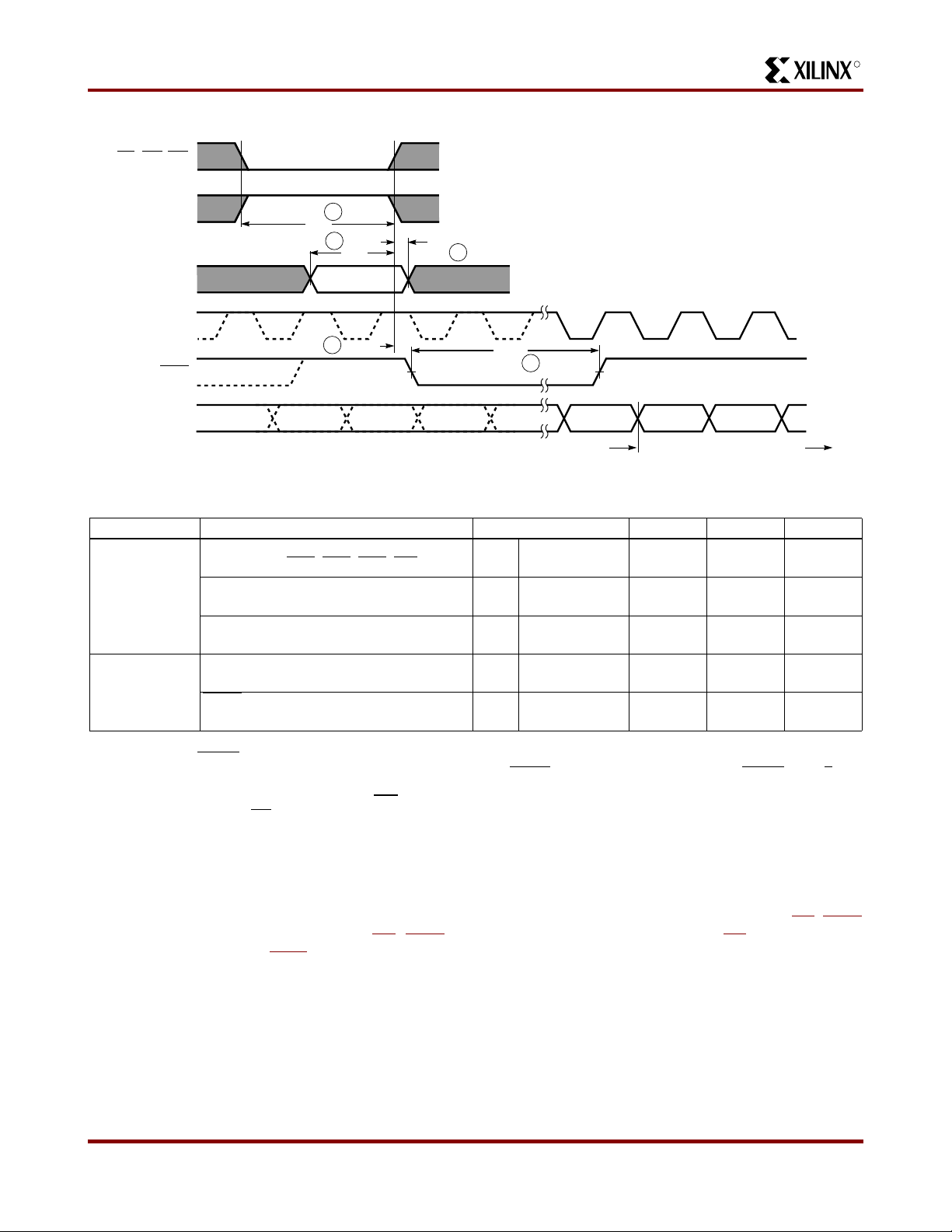
XC3000 Series Field Programmable Gate Arrays
WRITE TO FPGA
WS, CS0, CS1
R
RDY/BUSY
WRITE
CS2
D0-D7
CCLK
Effective Write time required
(Assertion of CS0
DIN Setup time required
DIN Hold time required
RDY/BUSY
delay after end of WS 4T
1
T
CA
2
T
DC
Valid
4
T
WTRB
T
CD
3
T
BUSY
6
D6DOUT
Previous Byte New Byte
D7 D0 D1 D2
X5992
Description S ymbol Min Max U nits
1T
CA
100 ns
, CS1, CS2, WS)
2
3
T
DC
T
CD
WTRB
60
0
60 ns
ns
ns
RDY
Earliest next WS
Low time generated 6 T
BUSY
after end of BUSY 5T
RBWT
BUSY
0ns
2.5 9 CCLK
periods
Notes: 1. At power-up, VCC must rise from 2.0 V to VCC min in less than 25 ms. If this is not possible, configuration can be delayed by
holding RESET
non-monotonically rising V
after V
2. Configuration must be del ayed until the INIT
CC
3. Time from end of WS
phase of the internal timing generator for CCLK.
4. CCLK and DOUT timing is test ed i n sl ave mode.
5. T
indicates that the double-buffered parallel-to-serial converter is not yet ready to receive new data. The shortest T
BUSY
occurs when a byte is loaded into an em pt y parallel-to-serial conver ter. The longest TBUSY occurs when a new word is
loaded into the input register before the second-level buffer has start ed shifting out data.
Note:
This timing diagram shows very relaxed requirements: Data need not be held beyond the rising edge of WS. BUSY
Low until VCC has reached 4.0 V (2.5 V for the XC3000L). A very long VCC rise time of >100 ms, or a
may require a >6-µs High level on RESET, followed by a >6-µs Low level on RESET and D/P
has reached 4.0 V (2.5 V for the XC3000L).
CC
of all FPGAs is High.
to CCLK cycle for the new byte of data depends on completion of previous byte processing and the
BUSY
will go active with in 60 ns after the end of WS . BUSY will stay active for several m icroseconds. WS may be asserted
immediately after the end of BUSY
.
Figure 28: Peripheral Mode Programming Switching Characteristics
7-30 November 9, 1998 (Version 3.1)
Page 29

R
Slave Serial Mode
In Slave Serial mode, an external signal drives the CCLK
input(s) of the FPGA( s). The serial co nfiguratio n bitstream
must be available at the DIN input of the lead FPGA a short
set-up time before each rising CCLK edge. The lead device
then presents the preamble data (and all data that over-
+5 V
Micro
Computer
STRB
D0
D1
I/O
Port
D2
D3
D4
D5
D6
D7
+5 V
XC3000 Series Field Programmable Gate Arrays
flows the le ad de vic e) o n i t s D OUT pi n. Th ere is an i nte rn al
delay of 0.5 CCLK periods, which means that DOUT
changes on the falling CCLK edge, and the next device in
the daisy-chain accepts data on the subsequent rising
CCLK edge.
*
GeneralPurpose
User I/O
Pins
If Readback is
Activated, a
5-kΩ Resistor is
Required in
Series with M1
Optional
Daisy-Chained
LCAs with
Different
Configurations
*
M0 M1 PWRDWN
CCLK
DIN
FPGA
D/P
INIT
Other
I/O Pins
5 kΩ
M2
DOUT
HDC
LDC
...
7
RESET
Figure 29: Slave Serial Mode Circuit Diagram
RESET
X5993
November 9, 1998 (Version 3.1) 7-31
Page 30

XC3000 Series Field Programmable Gate Arrays
R
DIN
1
CCLK
DOUT
(Output)
Bit n Bit n + 1
2
T
DCC
T
CCD
4
T
CCH
Description Symbol Min Max Units
T
To DOUT
DIN setup
CCLK
DIN hold
High time
Low time (Note 1)
Frequency
Notes: 1. The max limit of CCLK Low time is caused by dynamic circ ui try inside the FPGA.
2. Configuration must be del ayed until the INIT
3. At power-up, V
holding RESET
non-monotonically rising V
after V
CC
must rise from 2.0 V to VCC min in less than 25 ms. If this is not possible, configuration can be delayed by
CC
Low until VCC has reached 4.0 V (2.5 V for the XC3000L). A very long VCC rise time of >100 ms, or a
has reached 4.0 V (2.5 V for the XC3000L).
may require a >6-µs High level on RESET, followed by a >6-µs Low level on RESET and D/P
CC
of all FPGAs is High.
3
CCO
T
1
DCC
T
2
CCD
T
4
CCH
T
5
CCL
F
CC
5
T
CCL
3
T
CCO
Bit nBit n - 1
X5379
60
0
0.05
0.05
100
5.0
10
ns
ns
ns
µs
µs
MHz
Figure 30: Slave Serial Mode Programming Switching Characte ristics
7-32 November 9, 1998 (Version 3.1)
Page 31

R
XC3000 Series Field Programmable Gate Arrays
Program Readback Switching Characteristics
DONE/PROG
(OUTPUT)
1
T
RTH
RTRIG (M0)
2
T
RTCC
4
T
CCL
CCLK(1)
5
3
T
CCRD
4
T
CCL
M1 Input/
HI-Z
RDATA Output
Description Symbol Min Max Units
RTRIG RTRIG High 1 T
RTRIG setup
CCLK
RDATA
High time
delay
Low time
Notes: 1. During Readback, CCLK frequency may not exceed 1 MHz.
2. RETRIG (M0 positive t ransition) shall not be done until af ter one clock following active I/O pi ns.
3. Readback should not be i ni tiated until configuration is com pl ete.
4. T
is 5 µs min to 15 µs max for XC3000L.
CCLR
READBACK OUTPUT
VALID
RTH
T
2
RTCC
3
T
CCRD
4
T
CCHR
5
T
CCLR
VALID
READBACK OUTPUT
X6116
250 ns
200
0.5
0.5
100
5
ns
ns
µs
µs
7
November 9, 1998 (Version 3.1) 7-33
Page 32

XC3000 Series Field Programmable Gate Arrays
General XC3000 Series Switching Characteristics
4 T
MRW
RESET
2 T
M0/M1/M2
DONE/PROG
INIT
(Output)
PWRDWN
(Valid)
V
CC
MR
5 T
PGW
6 T
PGI
3 T
RM
Clear State Configuration StateUser State
Note 3
V
R
CCPD
X5387
Description Symbol Min Max Units
M0, M1, M2 setup time required
(2)
RESET
M0, M1, M2 hold time required
RESET Width (Low) req. for Abort
DONE/PROG
PWRDWN
Notes: 1. At power-up, VCC must rise from 2.0 V to VCC min in less than 25 ms. If this is not possible, configuration can be delayed by
holding RESET
non-monotonically rising V
after Vcc has reached 4.0 V (2.5 V for XC3000L).
2. RESET
specified hold time is caus ed by a shift-register filter slowi ng down the response to RESET
3. PWRDWN
Width (Low) required for Re-config.
INIT response after D/P is pulled Low
(3) Power Down V
Low until Vcc has reached 4.0 V (2.5 V for XC3000L). A very long Vcc rise time of >100 ms, or a
timing relative to valid mod e lines (M0, M1, M2) is relevant when RESET is us ed to delay configuration. The
transitions must occur while VCC >4.0 V(2.5 V for XC3000L).
CC
may require a >1-µs High level on RESET, followed by a >6-µs Low level on RESET and D/P
CC
2
3
4
5
6
T
T
T
T
T
V
MR
RM
MRW
PGW
PGI
CCPD
1
4.5
6
6
7
2.3 V
µs
µs
µs
µs
µs
during configuration.
7-34 November 9, 1998 (Version 3.1)
Page 33

R
XC3000 Series Field Programmable Gate Arrays
Device Performance
The XC3000 families of FPGAs can achieve very high performance. This is the result of
• A sub-micron manufacturing process, developed and
continuously being enhanced for the production of
state-of-the-art CMOS SRAMs.
• Careful optimization of transistor geometries, circuit
design, and lay-out, based on years of experience with
the XC3000 family.
• A look-up table based, coarse-grained architecture that
can collapse multiple-layer combinatorial logic into a
single function generator. One CLB can implement up
to four layers of conventional logic in as little as 1.5 ns.
Actual system performance is determined by the timing of
critical paths, including the delay through the combinatorial
and sequential logic elements within CLBs and IOBs, plus
the delay in the interconnect routing. The AC-timing specifications state the worst-case timing parameters for the various logic resources available in the XC3000-families
architecture. Figure 31 shows a variety of elements
involved in determining system performance.
Logic block performance is expressed as the propagation
time from the in te rc on n ec t p oin t at th e inp u t t o th e block to
the output of the block i n the i nter connec t area . Sinc e combinatorial logic is implemented with a memory lookup table
within a CLB, the combinatorial delay through the CLB,
called T
being implemented. For the combinatorial logic function
driving the data input of the storage element, the critical
timing is data set- up relativ e to the cloc k edge provided to
the flip-flop element. The delay from the clock source to the
output of the logic block is critical in the timing signals pro-
, is always the same, regardless of the function
ILO
duced by stora ge eleme nts . Load ing of a log ic- block outp ut
is limited only by the resulting propagation delay of the
larger interconnect network. Speed performance of the
logic block is a function of supply voltage and temperature.
See Figure 32.
Interconnect performance depends on the routing
resources used to implement the signal path. Direct interconnects to the neighboring CLB provide an extremely fast
path. Local interconnects go through switch matrices
(magic boxes) and suffer an RC delay, equal to the resistance of the pass transis tor mul tipli ed by the cap acita nce of
the driven metal line. Longlines carry the signal across the
length or breadth of the chip with only one access delay.
Generous on-chip signal buffering makes performance relatively insensitive to signal fan-out; increasing fan-out from
1 to 8 changes the CLB delay by only 10%. Clocks can be
distributed w ith two low-skew clock distribution networks.
The tools in the Development System used to place and
route a design in an XC 3000 FPGA automatica ll y cal cul a t e
the actual maximum worst-case delays along each signal
path. This timing information can be back-annotated to the
design’s netlist for use in timing simulation or examined
with, a static timing analyzer.
Actual syste m performance is applications dependent. The
maximum clock rate that can be used in a system is determined by the critical path delays within that system. These
delays are combinations of incremental logic and routing
delays, and vary from design to design. In a synchronous
system, the maximum clock rat e depends on the number of
combinatorial logic layers between re-synchronizing
flip-flops. Figure 33 shows the achievable clock rate as a
function of the number of CLB layers.
7
CLOCK
PAD
Clock to Output
T
CKO
(K)
T
PID
IOB
Combinatorial Setup
T
ILO
CLBCLB IOBCLB
T
ICK
LogicLogic
(K)
T
CKO
T
OKPO
T
OP
PAD
X3178
Figure 31: Primary Block Speed Factors. Actual timing is a function of various block factors combined with routing.
factors. Overall performance can be evaluated with the timing calculator or by an optional simulation.
November 9, 1998 (Version 3.1) 7-35
Page 34

XC3000 Series Field Programmable Gate Arrays
Figure 33: Clock Rate as a Function of Logic
Complexity (Number of Combinational Levels between
Flip-Flops)
1.00
R
SPECIFIED WORST-CASE VALUES
MMERCIAL (4.75 V)
0.80
0.60
NORMALIZED DELAY
0.40
0.20
– 55
– 40 – 20 0 25 40 70 80 100 125
Figure 32: Relative Del ay as a Function of Temperature, Supply Voltage and Processing Variations
300
250
200
150
100
XC3100A-3
System Clock (MHz)
50
XC3000A--6
0
CLB Levels:
Gate Levels:
4 CLBs
(4-16)
3 CLBs
(3-12)
2 CLBs
(2-8)
1 CLB
(1-4)
MAX CO
TYPICAL COMMERCIAL
(+ 5.0 V, 25°C)
TYPICAL MILITARY
MIN COMMERCIAL (4.75 V)
MIN COMMERCIAL (5.25 V)
TEMPERATURE (°C)
Power
Power Distribution
Power for the FPG A i s di st rib ut ed t hr ough a gr i d to ac hi ev e
high noise immunity and isolation between logic and I/O.
Inside the FPGA, a dedicated V
rounding the logic array provides power to the I/O drivers.
An independen t ma tri x o f V
interior logi c of the device. This power distribution grid provides a stable sup ply and g round for all internal lo gic, pro -
Toggle
Rate
X7065
viding the external package power pins are all connected
and appropriately decoupled. Typically a 0.1-µF capacitor
connected near the V
quate decoupling.
MAX MILITARY (4.5 V)
MIN MILITARY (4.5 V)
MIN MILITARY (5.5 V)
and ground ring sur-
CC
and groundlines supplie s the
CC
and ground pins will pro vide ade-
CC
Output buffers capable of driving the specified 4- or 8-mA
loads under worst-case conditions may be capable of driving as much as 25 to 30 times that current in a best case.
Noise can be reduced by minimizing external load capacitance and reducing simultaneous output transitions in the
same direction. It may also be beneficial to locate heavily
loaded output buffers near the ground pads. The I/O Block
output buffers have a slew-limited mode which should be
used where output r i se and f al l t i mes a re n ot s pee d cri t ic al .
Slew-limited outputs ma intain their dc drive capability, but
generate less external reflections and internal noise.
X6094
7-36 November 9, 1998 (Version 3.1)
Page 35

R
XC3000 Series Field Programmable Gate Arrays
Dynamic Power Consumption
XC3042A XC3042L XC3142A
One CLB driving three local interconnects 0.25 0.17 0.25 mW per MHz
One global cloc k buffer and clock line 2.25 1.40 1.70 mW per MHz
One device output with a 50 pF load 1.25 1.25 1.25 mW per MHz
Power Consumption
The Field Progr ammable Gat e Array e xhibit s the low power
consumption cha racteristic of CMOS ICs. For a ny design,
the configuration option of TTL chip input threshold
requires power for the threshold reference. The power
required by the static memory cells that hold the configuration data is very low and may be maintained in a
power-down mode.
Typ icall y, most of power dissipat ion is pr oduced by exter nal
capacitive loads on the output buffers. This load and frequency dependent power is 25 µW/pF/MHz per output.
Another compon en t of I/O power is the exte rn al dc loading
on all output pins.
Internal power dis sipation is a function of th e number and
size of the no des , an d t he fr eq uen cy a t w h ich th ey c han ge .
In an FPGA, the fraction of nodes changing on a given
clock is typically low (10-20%). For example, in a long
binary counter, the total activity of all counter flip-flops is
equivalent to th at of only two CLB ou tputs toggling at th e
clock frequency. Typical global clock-buffer power is
between 2.0 mW/MHz for the XC3020A and 3.5 mW/MHz
for the XC3090A. The internal capacitive load is more a
function of interconnect than fan-out. With a typical load of
three general interconnect segments, each CLB output
requires about 0.25 mW per MHz of its out put frequency.
Because the control storage of the FPGA is CMOS static
memory, its cells require a very low standby current for data
retention. In some sy stems, this low data ret ention cur rent
characteristic can be used as a method of preserving configurations in the event of a primary power loss. The FPGA
has built in powerdown logic which, when activated, will
disable normal operation of the device and retain only the
configuration data. All internal operation is suspended and
output buff ers are pl aced in t heir hig h-imped ance stat e with
no pull-ups. D i f f ere nt f ro m th e XC 30 00 fa mi l y whi ch ca n b e
powered down to a current consumption of a few microamps, the XC3100A draws 5 mA, even in power-down.
This makes power- down opera tion less m eani ngful . In contrast, I
for the XC3000L is only 10 µA.
CCPD
T o force the FPGA i nto t he Powerd own stat e, the us er must
pull the PWRDWN
tion voltage to the V
restored, V
and PWRDWN
pin Low and continue to supply a reten-
pins. When normal power is
is elevated to its normal operating voltage
CC
CC
is returned to a High. The FPGA resumes
operation with the same internal sequence that occurs at
the conclusi on of con fi g ur at ion. I n te rna l-I / O a nd log i c- bl ock
storage elements will be reset, the outputs will become
enabled and the DONE/PROG
When V
is shut down or disconnected, some power
CC
pin will be released.
might unintentionally be supplied from an incoming signal
driving an I/O pin. The conventional electrostatic input protection is implemented with diodes to the supply and
ground. A positive voltage applied to an input (or output)
will cause the positive protection diode to conduct and drive
the V
connection. This condition can produce invalid
CC
power conditions and should be avoided. A large series
resistor might be used to limit the current or a bipolar buffer
may be used to isolate the input signal.
7
November 9, 1998 (Version 3.1) 7-37
Page 36

XC3000 Series Field Programmable Gate Arrays
R
Pin Descriptions
Permanently Dedicated Pins
V
CC
Two to eight (depending on package type) connections to
the positive V supply voltage. All must be connected.
GND
Two to eight (depending on package type) connections to
ground. All must be connected.
PWRDWN
A Low on this CMOS-compatible input stops all internal
activity, but retains configuration. All flip -flops and latches
are reset, all outputs are 3-stated, and all inputs are interpreted as High, independent of their actual level. When
PWDWN
with DONE Low for two cycles of the internal 1-MHz clock.
Before and during configuration, PWRDWN
If not used, PWRDWN
RESET
This is an active Low input which has three functions.
Prior to the start of configuration, a Low input will delay the
start of the confi gurati on proces s. An intern al circ uit sense s
the application of power and begins a minimal time-out
cycle. When the time-out and RESET
levels of the M lines are sampled and configuration begins.
If RESET
re-initialized and restarts the configuration at the termination of RESET
If RESET
vides a global asynchronous RESET
storage elements of the FPGA.
CCLK
During confi gurat ion, Conf igur ation Cloc k is an output of an
FPGA in Master mode or Peripheral mode, but an input in
Slave mode. During Readback, CCLK is a clock input for
shifting con figuration data out of the FPGA.
CCLK drives dynamic circuitry inside the FPGA. The Low
time may, therefore, not ex ceed a f ew micro second s. When
used as an input, CCLK must be “parked High”. An internal
pull-up resistor maint ains High when the pin is not being
driven.
DONE/PROG
DONE is an open-drain output, configurable with or without
an internal pu ll-up resi stor of 2 to 8 k Ω. At the completion of
configuration, the FPGA circuitry becomes active in a synchronous order; DONE is programmed to go active High
one cycle either before or after the outputs go active.
returns High, the FPGA becomes operational
must be High.
must be tied to VCC.
are complete, the
is asserted during a configuration, the FPGA is
.
is asserted after configuration is complete, it pro-
of all IOB and CLB
(D/P)
Once configuration is done, a High-to-Low transition of this
pin will cause an initialization of the FPGA and start a
reconfiguration.
M0/RTRIG
As Mode 0, this i np ut i s sa mpl ed on powe r- on t o deter mi n e
the power-on delay (2
14
cycles if M0 is High, 216 cycles if M0
is Low). Before the start of configuration, this input is again
sampled together with M1, M2 to determine the configuration mode to be used.
A Low-to-High input transition, after configuration is complete, acts as a Read Trigger and initiates a Readback of
configuration and storage-element data clocked by CCLK.
By selecting t he app ropr i at e Rea dba ck o pti on w h en gen erating the bit stream, t his o peration may be l imite d to a si ngle
Readback, or be inhibited altogether.
M1/RDATA
As Mode 1, this input and M0, M2 are sampled before the
start of configuration to establish the configuration mode to
be used. If Read back is ne ver u sed, M1 ca n be t ied di rec tly
to ground or V
5-kΩ resistor to ground or V
. If Readback i s ev er us e d, M1 mu st us e a
CC
, to accommodate the
CC
RDATA output.
As an active-Low Read Data, after configuration is com-
plete, this pi n is the output of the Readback data.
User I/O Pins That Can Have Special
Functions
M2
During configuration, this input has a weak pull-up resistor.
Together with M0 and M1, it is sampled before the start of
configuration to establish the configuration mode to be
used. After configuration, this pin is a user-programmable
I/O pin.
HDC
During configuration, this output is held at a High level to
indicate that configuration is not yet complete. After configuration, this pin is a user-programmable I/O pin.
LDC
During Configuration, this output is held at a Low level to
indicate that the configuration is not yet complete. After
configuratio n, t his p in i s a use r- pr ogr amm abl e I/ O p i n. L DC
is particularl y useful in Maste r mode as a Low enable for an
EPROM, but it must then be programmed as a High after
configuration.
INIT
This is an activ e Low ope n-dra in outp ut w ith a we ak pul l-up
and is held Low d uring the po wer stabiliz ation and int ernal
clearing of t he co nfi gura tion me mory. It can be use d to indicate status t o a configurin g micropro cessor or, as a wired
7-38 November 9, 1998 (Version 3.1)
Page 37

R
XC3000 Series Field Programmable Gate Arrays
AND of several slave mode devices, a hold-off signal for a
master mode device. After configuration this pin becomes a
user-programmable I/O pin.
BCLKIN
This is a direct CMOS level input to the alternate clock
buffer (Auxiliary Buffer) in the lower right corner.
XTL1
This user I/O pin c an be used to operat e as the outp ut of an
amplifier driving an exte rn a l cryst al an d bia s circ uit ry.
XTL2
This user I/O pin can be used as the input of an amplifier
connected to an external crystal and bias circuitry. The I/O
Block is left unconfigured. The oscillator configuration is
activated by routing a net from the oscilla tor buffer symb ol
output and by the MakeBits program.
, CS1, CS2, WS
CS0
These four inputs represent a set of signals, three active
Low and one active High, that are used to control configuration-data entry in the Peripheral mode. Simultaneous
assertion of all four inputs generates a Write to the internal
data buffer. The removal of any assertion clocks in the
D0-D7 data. In Mas ter- P ar all e l mode , WS and CS 2 ar e the
A0 and A1 outputs. After configuration, these pins are
user-programmable I/O pins.
RDY/BUSY
During Peripheral Parallel mode configuration this pin indicates when the chip is ready for another byte of data to be
written to it. After configuration is complete, this pin
becomes a user- programmed I/O pin.
RCLK
During Master Parallel mode configuration, each change
on the A0-15 outputs is preceded by a rising edge on
, a redundant output signal. After configuration is
RCLK
complete, this pin becomes a user-programmed I/O pin.
D0-D7
This set of eight pins represents the parallel configuration
byte for the parallel Master and Peripheral modes. After
configuration is co mplete, they are user-program med I/O
pins.
A0-A15
During Master Parallel mode, these 16 pins present an
address output for a configura tion EPROM . After conf iguration, they are user -p ro gr a mm a ble I/O pins.
DIN
During Slave or Mast er Seria l confi guration , this pi n is used
as a serial-data input. In the Master or Peripheral configuration, this is the Data 0 input. Afte r configuration is co mplete, this pin becomes a user-programmed I/O pin.
DOUT
During configura t io n thi s pin is us ed to out put se rial - c onfi guration data to the DIN pin of a daisy-chained slave. After
configuration is complete, this pin becomes a user-programmed I/O pin.
TCLKIN
This is a direct CMO S-level input to the global clock buffer.
This pin can also be configured as a user programmable
I/O pin. Howe ver , s ince TCLKIN is the pr eferred i nput t o the
global clock net , and th e globa l clock ne t shoul d be use d as
the primary clock source, this pin is usually the clock input
to the chip.
Unrestricted User I/O Pins
I/O
An I/O pin may be programmed by the user to be an Input
or an Output pi n foll owing conf igura tio n. Al l unr estri cte d I/O
pins, plus the sp ecial pins men tioned on the followin g page,
have a weak pull-up resist or that becomes a ctive as soon
as the device powers up, and stays active until the end of
configuration.
7
Before and during configuration, all outputs that are not used for the configuration process are 3-stated with a weak
Note:
pull-up resistor.
November 9, 1998 (Version 3.1) 7-39
Page 38

XC3000 Series Field Programmable Gate Arrays
Pin Functions During Configuration
R
Configuration Mode <M2:M1:M0>
SLAVE
SERIAL
<1:1:1>
POWR
DWN
M1 (HIGH) (I) M1 (LOW) (I) M1 (LOW) (I) M1 (HIGH) (I) M1 (LOW) (I) 16 31 25 31 J2 52 49 B13 36 40 B14 45 48 RDATA
M0 (HIGH) (I) M0 (LOW) (I) M0 (HIGH) (I) M0 (LOW) (I) M0 (LOW) (I) 17 32 26 32 L1 54 51 A14 38 42 B15 47 50 RTRIG (I)
M2 (HIGH) (I) M2 (LOW) (I) M2 (HIGH) (I) M2 (HIGH) (I) M2 (HIGH) (I) 18 33 27 33 K2 56 53 C13 40 44 C15 49 56 I/O
HDC (HIGH) HDC (HIGH) HDC (HIGH) HDC (HIGH) HDC (HIGH) 19 34 28 34 K3 57 54 B14 41 45 E14 50 57 I/O
LDC (LOW) LDC (LOW) LDC (LOW) LDC (LOW) LDC (LOW) 20 36 30 36 L3 59 56 D14 45 49 D16 54 61 I/O
INIT* INIT* INIT* INIT* INIT* 22403442K66562G145359H156577 I/O
GND GND GND GND GND 23 41 35 43 J6 66 63 H12 55 61 J14 67 79 GND
RESET (I) RESET (I) RESET (I) RESET (I) RESET (I) 27 48 44 54 K10 78 75 P14 71 78 R15 87 102 RESET (I)
DONE DONE DONE DONE DONE 28 49 45 55 J10 80 77 N13 73 80 R14 89 107 PROGRAM (I)
DIN (I) DIN (I) DAT A 0 (I) DATA 0 (I) DATA 0 (I) 38 62 58 72 B11 100 97 N2 106 119 R3 130 151 I/O
DOUT DOUT DOUT DOUT DOUT 39 63 59 73 C10 1 98 M3 107 120 N4 131 152 I/O
CCLK (I) CCLK (O) CCLK (O) CCLK (O) CCLK (O) 40 64 60 74 A11 2 99 P1 108 121 R2 132 153 CCLK (I)
Notes: X** X X X XC3195A
MASTER-
SERIAL
<0:0:0>
POWER
(I)
DWN
(I)
PERIPH
<1:0:1>
POWER
DWN
DATA 7 (I) DATA 7 (I) DATA 7 (I) 50 46 56 K11 81 78 M12 74 81 N13 90 109 I/O
DATA 6 (I) DATA 6 (I) DATA 6 (I) 52 48 58 H10 83 80 N11 78 86 P12 96 115 I/O
DATA 5 (I) DATA 5 (I) DATA 5 (I) 53 49 60 F10 87 84 M9 84 92 T11 102 122 I/O
CS0 (I) 54 50 61 G10 88 85 N9 85 93 R10 103 123 I/O
DATA 4 (I) DATA 4 (I) DATA 4 (I) 55 51 62 G11 89 86 N8 88 96 R9 108 128 I/O
DATA 3 (I) DATA 3 (I) DATA 3 (I) 57 53 65 F11 92 89 N7 92 102 P8 112 132 I/O
CS1 (I) 58 54 66 E11 93 90 P6 93 103 R8 113 133 I/O
DATA 2 (I) DATA 2 (I) DATA 2 (I) 59 55 67 E10 94 91 M6 96 106 R7 118 138 I/O
DATA 1 (I) DATA 1 (I) DATA 1 (I) 60 56 70 D10 98 95 M5 102 114 R5 124 145 I/O
RDY/BUSY RCLK RCLK 61 57 71 C11 99 96 N4 103 115 P5 125 146 I/O
WS (I) A0 A0 1 61 75 B10 5 2 M2 111 124 P2 135 161 I/O
CS2 (I) A1 A1 2 62 76 B9 6 3 N1 112 125 M3 136 162 I/O
MASTER-
HIGH
<1:1:0>
POWER
(I)
DWN
(I)
A2 A2 3 63 77 A10 8 5 L2 115 128 P1 140 165 I/O
A3 A3 4 64 78 A9 9 6 L1 116 129 N1 141 166 I/O
A15 A15 65 81 B6 12 9 K1 119 132 M1 146 172 5
A4 A4 5 66 82 B7 13 10 J2 120 133 L2 147 173 I/O
A14 A14 6 67 83 A7 14 11 H1 123 136 K2 150 178 I/O
A5 A5 7 68 84 C7 15 12 H2 124 137 K1 151 179 I/O
A13 A13 9 2 2 A6 17 14 G2 128 141 H2 156 184 I/O
A6 A6 10 3 3 A5 18 15 G1 129 142 H1 157 185 I/O
A12 A12 11 4 4 B5 19 16 F2 133 147 F2 164 192 I/O
A7 A7 12 5 5 C5 20 17 E1 134 148 E1 165 193 I/O
A11 A11 13 6 8 A3 23 20 D1 137 151 D1 169 199 I/O
A8 A8 14 7 9 A2 24 21 D2 138 152 C1 170 200 I/O
A10 A10 15 8 10B325 22B1141155E3173203 I/O
A9 A9 16 9 11 A1 26 26 C2142156C2174204 I/O
MASTER-
LOW
<1:0:0>44PLCC64VQFP68PLCC84PLCC84PGA
POWER
DWN
*** ** ****
100
100
VQFP
132
144
160
175
PQFP
TQFP
PGA
TQFP
PQFP
(I) 7 17 10 12 B2 29 26 A1 1 159 B2 1 3
26 47 43 53 L11 76 73 M13 69 76 P15 85 100 XTL2 OR I/O
30 51 47 57 J11 82 79 P13 75 82 T14 91 110 XTL1 OR I/O
X X X X X X X XC3x30A etc.
X X X X XC3x20A etc.
XXX XXX XC3x42A etc.
X** X X XC3x64A etc.
X** X X X X X XC3x90A etc.
PGA
176
TQFP
PQFP
208
User
Function
POWER
DWN
(1)
All Others
Generic I/O pins are not shown.
For a detailed description of the configuration modes, see page25 through page 34.
For pinout details, see page 65 through page 76.
Represents a weak pull-up before and during configuration.
INIT is an open drain output during configuration.
*
Represents an input.
(I)
Pin assignment for the XC3064A/XC3090A and XC3195A differ from those shown.
**
Peripheral mode and master parallel mode are not supported in the PC44 package.
***
Pin assignments for the XC3195A PQ208 differ from those shown.
****
Pin assignments of PGA Footprint PLCC sockets and PGA packages are not identical.
The information on this page is provided as a convenient summary. For detailed pin descriptions, see the preceding two pages.
Note
Before and during configuration, all outputs that are not used for the configuration process are 3-stated with a weak pull-up resistor.
:
7-40 November 9, 1998 (Version 3.1)
Page 39

R
XC3000 Series Field Programmable Gate Arrays
XC3000A Switching Characteristics
Xilinx maintains test specifications for each product as controlled documents. To insure the use of the most recently released
device perfo rmance parameters, please request a copy of the current t e st-specification revision.
XC3000A Operating Conditions
Symbol Description Min Max Units
V
CC
V
IHT
V
ILT
V
IHC
V
ILC
T
IN
Note: At junction tem peratures above those listed as Operating Conditions, all delay paramet ers increase by 0.3% per °C.
XC3000A DC Characteristics Over Operating Conditions
Supply voltage relative to GND Comme rc ial 0°C to +85°C junction 4.75 5.25 V
Supply voltage relative to GND Industrial -40°C to +100°C junction 4.5 5.5 V
High-level input voltage — TTL configuration 2.0 V
CC
Low-level input voltage — TTL configuration 0 0.8 V
High-level input voltage — CMOS configuration 70% 100% V
Low-level input voltage — CMOS configuration 0 20% V
Input signal transition time 250 ns
V
CC
CC
Symbol Description Min Max Units
V
V
V
V
V
CCPD
I
CCPD
I
CCO
I
OH
OL
OH
OL
IL
High-level output voltage (@ IOH = –4.0 mA, VCC min)
Low-level output voltage (@ IOL = 4.0 mA, VCC min) 0.40 V
High-level output voltage (@ IOH = –4.0 mA, VCC min)
Low-level output voltage (@ IOL = 4.0 mA, VCC min) 0.40 V
Commercial
Industrial
Power-down supply voltage (PWRDWN mus t be Low) 2.30 V
Power-down supply current
(V
CC(MAX)
@ T
) 3020A
MAX
3030A
3042A
3064A
3090A
Quiescent FPGA supply current in addition to I
CCPD
Chip thresholds programmed as CMOS levels
Chip thresholds programmed as TTL levels
Input Leakage Current –10 +10 µA
3.86 V
3.76 V
100
160
240
340
500
500
10
Input capaci tance, all packages except PGA175
(sample tested)
All Pins except XTL1 and XTL2
C
IN
XTL1 and XTL2
Input capacitance, PGA 175
10
15
(sample tested)
All Pins except XTL1 and XTL2
XTL1 and XTL2
I
I
RIN
RLL
Pad pull-up (when selected) @ VIN = 0 V
Horizontal Longline pull-up (when selected) @ logic Low 3.4 mA
3
Notes: 1. With no output current loads, no active input or Longline pull-up resistors, all package pins at V
device configured with a tie option.
2. T otal continuous output sink current may not exceed 100 mA per ground pin. T otal continuous output source may not exceed
100 mA per V
3. Not tested. Allow an undriven pin to float High. For any other purposes use an external pull-up.
pin. The number of ground pins varies from the XC3020A to the XC3090A.
CC
0.02 0.17 mA
or GND, and the FPGA
CC
16
20
7
µA
µA
µA
µA
µA
µA
µA
pF
pF
pF
pF
November 9, 1998 (Version 3.1) 7-41
Page 40
XC3000 Series Field Programmable Gate Arrays
XC3000A Absolute Maximum Ratings
Symbol Description Units
Supply voltage relative to GND –0.5 to +7.0 V
Input voltage with respect to GND –0.5 to VCC +0.5 V
Voltage applied to 3-state output –0.5 to VCC +0.5 V
Storage temperature (ambient) –65 to +150 °C
Maximum soldering tem p er at ur e (1 0 s @ 1/1 6 in.) +260 °C
Junction temper at ur e pla st i c +125 °C
Junction temperature ceramic +150 °C
T
T
V
V
V
STG
T
CC
IN
TS
SOL
J
R
Note: Stresses beyond thos e l is ted under Absolute Maximum Ratings may cause permanent damage to the device. These are
stress ratings only, and functional operation of the device at these or any other conditions bey ond those listed under
Recommended Operating Conditions is not implied. Exposure to Absolute Maximum Ratings conditions for extended
periods of time may affect device reliability.
XC3000A Global Buffer Switching Characteristics Guidelines
Speed Grade -7 -6
Description Symbol Max Max Units
Global and Alternate Clock Distribution
Either: Normal IOB input pad through clock buffer
to any CLB or IOB clock input
Or: Fast (CMOS only) input pad through clock
buffer to any CLB or IOB clock input
TBUF driving a Horizontal Longline (L.L.)
I to L.L. while T is Low (buffer ac tive)
T↓ to L.L. active and valid with single pull-up resistor
T↓ to L.L. active and valid with pair of pull-up resistors
T↑ to L.L. High with single pull-up resist or
T↑ to L.L. High with pair of pull-up resistors
BIDI
Bidirectional buffer delay T
Note: 1. Timing is based on the XC3042A, for other devices see timing calcu la to r.
1
T
PID
T
1
PIDC
T
T
T
T
PUS
T
PUF
BIDI
IO
ON
ON
7.5
6.0
4.5
9.0
11.0
16.0
10.0
1.7 1.5 ns
7.0
5.7
4.0
8.0
10.0
14.0
8.0
ns
ns
ns
ns
ns
ns
ns
7-42 November 9, 1998 (Version 3.1)
Page 41

R
XC3000 Series Field Programmable Gate Arrays
XC3000A CLB Switching Characteristics Guidelines
Testing of the switchin g parameters is modeled after testing methods specified by MIL-M-38510/605. All devices are 100%
functionally tested. Since many internal timing parameters cannot be measured directly, they are derived from benchmark
timing patterns. The following guidelines reflect worst-case values over the recommended operating conditions. For more
detailed, more precise, and more up-to-date timing information, use the values provided by the timing calculator and used
in the simulator.
Speed Grade -7 -6
Description Symbol Min Max Min Max Units
Combinatorial Delay
Logic Variables A, B, C, D, E, to outputs X or Y
FG Mode
F and FGM Mode
Sequential delay
Clock k to outputs X or Y
Clock k to outputs X or Y when Q is returned
through function generators F or G to drive X or Y
FG Mode
F and FGM Mode
Set-up time before clock K
Logic Variables A, B, C, D, E
FG Mode
F and FGM Mode
Data In DI
Enable Clock EC
Hold Time after clock K
Logic Variables A, B, C, D, E
Data In DI
2
Enable Clock EC
Clock
Clock High time
Clock Low time
Max. flip-flop toggle rate
Reset Direct (RD)
RD width
delay from RD to outputs X or Y
1
Global Reset (RESET
Pad)
RESET width (Low)
delay from RESET
Notes:
1. Timing is based on the XC3042A, for other devi ces see timing calculator.
2. The CLB K to Q output delay (T
Data In hold time requirement (T
pad to outputs X or Y
, #8) of any CLB, plus the shortest possible interconnect delay, is always longer than the
CKO
, #5) of any CLB on the same die.
CKDI
1T
8T
2
4
6
3
5
7
11
12
13
9
T
T
T
T
ECCK
T
T
T
CKEC
T
T
F
T
T
T
T
ILO
CKO
QLO
ICK
DICK
CKI
CKDI
CH
CL
CLK
RPW
RIO
MRW
MRQ
4.5
5.0
4.0
4.5
0
1.0
2.0
4.0
4.0
113.0
6.0
16.0
5.1
5.6
4.5
9.5
10.0
3.5
4.0
3.0
4.0
0
1.0
2.0
3.5
3.5
135.0
5.0
6.0
14.0
19.0
4.1
4.6
4.0
8.0
8.5
5.0
17.0
ns
ns
ns
ns
ns
ns
ns
ns
ns
ns
ns
ns
ns
ns
MHz
ns
ns
ns
ns
7
November 9, 1998 (Version 3.1) 7-43
Page 42

XC3000 Series Field Programmable Gate Arrays
XC3000A CLB Switching Characteristics Guidelines (continued)
CLB Output (X, Y)
(Combinatorial)
T
1
ILO
CLB Input (A,B,C,D,E)
R
CLB Clock
CLB Input
(Direct In)
CLB Input
(Enable Clock)
CLB Output
(Flip-Flop)
CLB Input
(Reset Direct)
CLB Output
(Flip-Flop)
T
2
ICK
T
12
CL
T
4
DICK
T
6
ECCK
T
13
RPW
RIO
T
T
9
11
T
3
CKI
T
CH
T
5
CKDI
T
7
CKEC
T
8
CKO
X5424
7-44 November 9, 1998 (Version 3.1)
Page 43

R
XC3000 Series Field Programmable Gate Arrays
XC3000A IOB Switching Characteristics Guidelines
Testing of the switchin g parameters is modeled after testing methods specified by MIL-M-38510/605. All devices are 100%
functionally tested. Since many internal timing parameters cannot be measured directly, they are derived from benchmark
timing patterns. The following guidelines reflect worst-case values over the recommended operating conditions. For more
detailed, more precise, and more up-to-date timing information, use the values provided by the timing calculator and used
in the simulator.
Speed Grade -7 -6
Description Symbol Min Max Min Max Units
Propagation Delays (Input)
Pad to Direct In (I)
Pad to Registered In (Q) with latch transparent
Clock (IK) to Registered In (Q)
3
4
T
T
T
PID
PTG
IKRI
4.0
15.0
3.0
Set-up Time (Input)
Pad to Clock (IK) set-up time 1 T
PICK
14.0 12.0 ns
Propagation Delays (Output)
Clock (OK) to Pad (fast)
same (slew rate limited)
Output (O) to Pad (fast)
same (slew-rate limited)
3-state to Pad begin hi-Z (fast)
same (slew-rate limited)
3-state to Pad a ctive and valid (fast)
same (slew -rate limited)
10
10
7
7
9
9
8
8
OKPO
T
OKPO
T
T
T
TSHZ
T
TSHZ
T
TSON
T
TSON
OPF
OPS
8.0
18.0
6.0
16.0
10.0
20.0
11.0
21.0
T
Set-up and Hold Times (Output)
Output (O) to clock (OK) set-up time
Output (O) to clock (OK) hold time
5
T
OOK
T
6
OKO
8.0
0
7.0
0
Clock
Clock High time
Clock Low time
Max. flip-flop toggle rate
11
12
F
T
T
IOH
IOL
CLK
4.0
4.0
113.0
3.5
3.5
135.0
Global Reset Delays (based on XC3042A)
RESET
RESET
Pad to Registered In (Q)
Pad to output pad (fast)
(slew-rate limited)
Notes: 1. Timing is measured at pin threshold, with 50 pF exte rnal capacitive loads (incl. test fi xture). Typical slew rate limited output
rise/fall times are approxi m ately four times longer.
2. Voltage levels of unused (bonded and unbonded) pads must be valid logic levels . Ea ch can be configured with the internal
pull-up resistor or alternatively configured as a driven output or driven from an external source.
3. Input pad set-up tim e is specified with respect to the internal clock (ik). In order to cal culate system set-up time, subtract
clock delay (pad to ik) from the in put pad set-up time value. Input pad holdt i me with respect to the internal cloc k (i k) is
negative. This means that pad level changes immediately before the internal clock edge (ik) wil l no t be rec ognized.
, T
4. T
PID
PTG
, and T
are 3 ns higher for XTL2 when the pin is configured as a user input.
PICK
13
15
15
T
T
T
RRI
RPO
RPO
24.0
33.0
43.0
3.0
14.0
2.5
7.0
15.0
5.0
13.0
9.0
12.0
10.0
18.0
23.0
29.0
37.0
ns
ns
ns
ns
ns
ns
ns
ns
ns
ns
ns
ns
ns
ns
ns
MHz
ns
ns
ns
7
November 9, 1998 (Version 3.1) 7-45
Page 44

XC3000 Series Field Programmable Gate Arrays
XC3000A IOB Switching Characteristics Guidelines (continued)
I/O Block (I)
T
3
PID
I/O Pad Input
T
1
PICK
I/O Clock (IK/OK)
I/O Block (RI)
RESET
I/O Block (O)
I/O Pad Output
(Direct)
I/O Pad Output
(Registered)
T
12
IOL
T
5
OOK
T
10
OP
11
T
4
IKRI
T
6
OKO
R
T
IOH
T
13
RRI
T
15
RPO
T
7
OKPO
I/O Pad TS
I/O Pad Output
3- STATE
(OUTPUT ENABLE)
OUT
DIRECT IN
REGISTERED IN
T
O
I
Q
OUT
INVERT
T
8
TSON
PROGRAM-CONTROLLED MEMORY CELLS
3-STATE
INVERT
IKOK
FLIP
FLOP
R
FLIP
FLOP
or
LATCH
R
OUTPUT
SELECT
QD
DQ
SLEW
RATE
TTL or
CMOS
INPUT
THRESHOLD
OUTPUT
BUFFER
9
PASSIVE
PULL UP
T
TSHZ
X5425
Vcc
I/O PAD
(GLOBAL RESET)
CK1
PROGRAM
CONTROLLED
MULTIPLEXER
=
PROGRAMMABLE INTERCONNECTION POINT or PIP
CK2
X3029
7-46 November 9, 1998 (Version 3.1)
Page 45

R
XC3000 Series Field Programmable Gate Arrays
XC3000L Switching Characteristics
Xilinx maintains test specifications for each product as controlled documents. To insure the use of the most recently released
device perfo rmance parameters, please request a copy of the current t e st-specification revision.
XC3000L Operating Conditions
Symbol Description Min Max Units
Supply voltage relative to GND Comme rc ial 0°C to +85°C junction 3.0 3.6 V
V
CC
V
IH
V
IL
T
IN
Notes: 1. At junction temperatures above those listed as Operating Conditio ns, all delay parameters increase by 0.3% per °C.
2. Although the present (1996) devices operate over the full supply voltage range from 3.0 to 5.25 V, Xilinx reserves the right to
XC3000L DC Characteristics Over Operating Condition s
Symbol Description Min Max Units
V
OH
V
OL
V
OH
V
OL
V
CCPD
I
CCPD
I
CCO
I
IL
C
IN
I
RIN
I
RLL
Notes: 1. With no output current loads, no active input or Longline pull-up resistors, all package pins at V
2. T otal continuous output sink current may not exceed 100 mA per ground pin. T otal continuous output source may not exceed
3. Not tested. Allows an undriven p in to float High. For any other purpose, use an exter nal pul l -up.
High-level input voltage — TTL configuration 2.0 VCC+0.3 V
Low-level input voltage — TTL conf igu ratio n -0.3 0.8 V
Input signal transition time 250 ns
restrict operation to the 3.0 to 3.6 V range later, when smaller device geometries might preclud e o peration at 5V. Operating
conditions are guaranteed i n the 3.0 – 3.6 V V
CC
range.
High-level output voltage (@ IOH = –4.0 mA, VCC min) 2.40 V
Low-level output voltage (@ IOL = 4.0 mA, VCC min) 0.40 V
High-level output voltage (@ IOH = –4.0 mA, VCC min) VCC -0.2 V
Low-level output voltage (@ IOL = 4.0 mA, VCC min) 0.2 V
Power-down supply voltage (PWRDWN mus t be Low) 2.30 V
Power-down supply current (V
CC(MAX)
Quiescent FPGA supply current in addition to I
@ T
)10µA
MAX
CCPD
1
Chip thresholds programmed as CMOS levels 20 µA
Input Leakage Current –10 +10 µA
Input capaci tance, all packages except PGA175
(sample tested)
All Pins except XTL1 and XTL2
XTL1 and XTL2
10
15
pF
pF
Input capacitance, PGA 175
(sample tested)
All Pins except XTL1 and XTL2
XTL1 and XTL2
15
20
pF
pF
Pad pull-up (when selected) @ VIN = 0 V3 0.01 0.17 mA
Horizontal Lo ngline pull-up (when selected) @ logic Low 2.50 mA
or GND, and the FPGA
device configured with a tie option. I
100 mA per V
pin. The number of ground pins varies from the XC3020L to the XC3090L.
CC
is in addition to I
CCO
CCPD
.
CC
7
November 9, 1998 (Version 3.1) 7-47
Page 46

XC3000 Series Field Programmable Gate Arrays
XC3000L Absolute Maximum Ratings
Symbol Description Units
Supply voltage relative to GND –0.5 to +7.0 V
Input voltage with respect to GND –0.5 to VCC +0.5 V
Voltage applied to 3-state output –0.5 to VCC +0.5 V
Storage temperature (ambient) –65 to +150 °C
Maximum soldering tem p er at ur e (1 0 s @ 1/1 6 in.) +260 °C
Junction temper at ur e pla st i c +125 °C
Junction temperature ceramic +150 °C
T
T
V
V
V
STG
T
CC
IN
TS
SOL
J
R
Note: Stresses beyond thos e l is ted under Absolute Maximum Ratings may cause permanent damage to the device. These are
stress ratings only, and functional operation of the device at these or any other conditions bey ond those listed under
Recommended Operating Conditions is not implied. Exposure to Absolute Maximum Ratings conditions for extended
periods of time may affect device reliability.
XC3000L Global Buffer Switching Characteristics Guidelines
Speed Grade -8
Description Symbol Max Units
Global and Alternate Clock Distribution
Either: Normal IOB input pad through clock buffer
to any CLB or IOB clock input
Or: Fast (CMOS only) input pad through clock
buffer to any CLB or IOB clock input
TBUF driving a Horizontal Longline (L.L.)
I to L.L. while T is Low (buffer ac tive)
T↓ to L.L. active and valid with single pull-up resistor
T↑ to L.L. High with single pull-up resist or
BIDI
Bidirectional buffer delay T
Notes: 1. Timing is based on the XC3042A, for other devices see t imi ng calculator.
2. The use of two pull-up resist ors per Longline, available on other XC3000 devices, is not a valid option for XC3000L devices.
1
T
PID
T
1
PIDC
T
T
T
IO
ON
PUS
BIDI
9.0
7.0
5.0
12.0
24.0
2.0 ns
ns
ns
ns
ns
ns
7-48 November 9, 1998 (Version 3.1)
Page 47

R
XC3000 Series Field Programmable Gate Arrays
XC3000L CLB Switching Characteristics Guidelines
Testing of the switchin g parameters is modeled after testing methods specified by MIL-M-38510/605. All devices are 100%
functionally tested. Since many internal timing parameters cannot be measured directly, they are derived from benchmark
timing patterns. The following guidelines reflect worst-case values over the recommended operating conditions. For more
detailed, more precise, and more up-to-date timing information, use the values provided by the timing calculator and used
in the simulator.
Speed Grade -8
Description Symbol Min Max Units
Combinatorial Delay
Logic Variables A, B, C, D, E, to outputs X or Y
FG Mode
F and FGM Mode
Sequential delay
Clock k to outputs X or Y
Clock k to outputs X or Y when Q is returned
through function generators F or G to drive X or Y
FG Mode
F and FGM Mode
Set-up time before clock K
Logic Variables A, B, C, D, E
FG Mode
F and FGM Mode
Data In DI
Enable Clock EC
Hold Time after clock K
Logic Variables A, B, C, D, E
Data In DI
2
Enable Clock EC
Clock
Clock High time
Clock Low time
Max. flip-flop toggle rate
Reset Direct (RD)
RD width
delay from RD to outputs X or Y
1
Global Reset (RESET
Pad)
RESET width (Low)
delay from RESET
Notes:
1. Timing is based on the XC3042L, for other d evi ces see timing calculator.
2. The CLB K to Q output delay (T
Data In hold time requirement (T
pad to outputs X or Y
, #8) of any CLB, plus the shortest possible interconnect delay, is always longer than the
CKO
, #5) of any CLB on the same die.
CKDI
1T
8T
2
4
6
3
5
7
11
12
13
9
T
T
T
DICK
T
ECCK
T
T
CKDI
T
CKEC
T
T
F
T
RPW
T
T
MRW
T
MRQ
ILO
CKO
QLO
ICK
CKI
CH
CL
CLK
RIO
6.7
7.5
7.5
14.0
14.8
5.0
5.8
5.0
6.0
0
2.0
2.0
5.0
5.0
80.0
7.0
7.0
16.0
23.0
ns
ns
ns
ns
ns
ns
ns
ns
ns
ns
ns
ns
ns
ns
MHz
ns
ns
ns
ns
7
November 9, 1998 (Version 3.1) 7-49
Page 48

XC3000 Series Field Programmable Gate Arrays
XC3000L CLB Switching Characteristics Guidelines (continued)
CLB Output (X, Y)
(Combinatorial)
T
1
ILO
CLB Input (A,B,C,D,E)
R
CLB Clock
CLB Input
(Direct In)
CLB Input
(Enable Clock)
CLB Output
(Flip-Flop)
CLB Input
(Reset Direct)
CLB Output
(Flip-Flop)
T
2
ICK
T
12
CL
T
4
DICK
T
6
ECCK
T
13
RPW
RIO
T
T
9
11
T
3
CKI
T
CH
T
5
CKDI
T
7
CKEC
T
8
CKO
X5424
7-50 November 9, 1998 (Version 3.1)
Page 49

R
XC3000 Series Field Programmable Gate Arrays
XC3000L IOB Switching Characteristics Guidelines
Testing of the switchin g parameters is modeled after testing methods specified by MIL-M-38510/605. All devices are 100%
functionally tested. Since many internal timing parameters cannot be measured directly, they are derived from benchmark
timing patterns. The following guidelines reflect worst-case values over the recommended operating conditions. For more
detailed, more precise, and more up-to-date timing information, use the values provided by the timing calculator and used
in the simulator.
Speed Grade -8
Description Symbol Min Max Units
Propagation Delays (Input)
Pad to Direct In (I)
Pad to Registered In (Q) with latch transparent
Clock (IK) to Registered In (Q)
Set-up Time (Input)
Pad to Clock (IK) set-up time 1 T
Propagation Delays (Output)
Clock (OK) to Pad (fast)
same (slew rate limited)
Output (O) to Pad (fast)
same (slew-rate limited)
3-state to Pad begin hi-Z (fast)
same (slew-rate limited)
3-state to Pad a ctive and valid (fast)
same (slew -rate limited)
Set-up and Hold Times (Output)
Output (O) to clock (OK) set-up time
Output (O) to clock (OK) hold time
Clock
Clock High time
Clock Low time
Max. flip-flop toggle rate
Global Reset Delays (based on XC3042L)
RESET
RESET
Pad to Registered In (Q)
Pad to output pad (fast)
(slew-rate limited)
Notes:
1. Timing is measured at pin threshold, with 50 pF external capacitive loads (incl. test fixture). Typical slew rate limited output
rise/fall times are approxi m ately four times longer.
2. Voltage levels of unused (bonded and unbonded) pads must be valid logic levels . Ea ch can be configured with the internal
pull-up resistor or alternatively configured as a driven output or driven from an external source.
3. Input pad set-up tim e is specified with respect to the internal clock (ik). In order to cal culate system set-up time, subtract
clock delay (pad to ik) from the in put pad set-up time value. Input pad holdt i me with respect to the internal cloc k (i k) is
negative. This means that pad level changes immediately before the internal clock edge (ik) wil l no t be rec ognized.
, T
4. T
PID
PTG
, and T
are 3 ns higher for XTL2 when the pin is conf i gured as a user input.
PICK
10
10
11
12
13
15
15
3
4
7
7
9
9
8
8
5
6
T
T
PTG
T
PICK
T
OKPO
T
OKPO
T
OPF
T
OPS
T
TSHZ
T
TSHZ
T
TSON
T
TSON
T
OOK
T
OKO
T
T
F
T
T
RPO
T
RPO
PID
IKRI
IOH
IOL
CLK
RRI
22.0 ns
12.0
0
5.0
5.0
80.0
5.0
24.0
6.0
12.0
28.0
9.0
25.0
12.0
28.0
16.0
32.0
25.0
35.0
51.0
ns
ns
ns
ns
ns
ns
ns
ns
ns
ns
ns
ns
ns
ns
ns
MHz
ns
ns
ns
7
November 9, 1998 (Version 3.1) 7-51
Page 50

XC3000 Series Field Programmable Gate Arrays
XC3000L IOB Switching Characteristics Guidelines (continued )
I/O Block (I)
T
3
PID
I/O Pad Input
T
1
PICK
I/O Clock (IK/OK)
I/O Block (RI)
RESET
I/O Block (O)
I/O Pad Output
(Direct)
I/O Pad Output
(Registered)
T
12
IOL
T
5
OOK
T
10
OP
11
T
4
IKRI
T
6
OKO
R
T
IOH
T
13
RRI
T
15
RPO
T
7
OKPO
I/O Pad TS
I/O Pad Output
3- STATE
(OUTPUT ENABLE)
OUT
DIRECT IN
REGISTERED IN
T
O
I
Q
OUT
INVERT
T
8
TSON
PROGRAM-CONTROLLED MEMORY CELLS
3-STATE
INVERT
IKOK
FLIP
FLOP
R
FLIP
FLOP
or
LATCH
R
OUTPUT
SELECT
QD
DQ
SLEW
RATE
TTL or
CMOS
INPUT
THRESHOLD
OUTPUT
BUFFER
9
PASSIVE
PULL UP
T
TSHZ
X5425
Vcc
I/O PAD
(GLOBAL RESET)
CK1
PROGRAM
CONTROLLED
MULTIPLEXER
=
PROGRAMMABLE INTERCONNECTION POINT or PIP
CK2
X3029
7-52 November 9, 1998 (Version 3.1)
Page 51

R
XC3000 Series Field Programmable Gate Arrays
XC3100A Switching Characteristics
Xilinx maintains test specifications for each product as controlled documents. To insure the use of the most recently released
device perfo rmance parameters, please request a copy of the current t e st-specification revision.
XC3100A Operating Conditions
Symbol Description Min Max Units
Supply voltage relative to GND Comme rc ial 0°C to +85°C junction 4.25 5.25 V
V
CC
V
IHT
V
ILT
V
IHC
V
ILC
T
IN
Note: At junction tem peratures above those listed as Operating Conditions, all delay paramet ers increase by 0.3% per °C.
XC3100A DC Characteristics Over Operating Conditions
Supply voltage relative to GND Industrial -40°C to +100°C junction 4.5 5.5 V
High-level input voltage — TTL configuration 2.0 V
CC
Low-level input voltage — TTL configuration 0 0.8 V
High-level input voltage — CMOS configuration 70% 100% V
Low-level input voltage — CMOS configuration 0 20% V
Input signal transition time 250 ns
V
CC
CC
Symbol Description Min Max Units
V
V
V
V
V
CCPD
I
CCO
I
OH
OL
OH
OL
IL
High-level output voltage (@ IOH = –8.0 mA, VCC min)
Low-level output voltage (@ IOL = 8.0 mA, VCC min) 0.40 V
High-level output voltage (@ IOH = –8.0 mA, VCC min)
Low-level output voltage (@ IOL = 8.0 mA, VCC min) 0.40 V
Commercial
Industrial
Power-down supply voltage (PWRDWN mus t be Low) 2.30 V
Quiescent LCA supply current in addition to I
CCPD
1
Chip thresholds programmed as CMOS levels
Chip thresholds programmed as TTL levels
Input Leakage Current –10 +10 µA
3.86 V
3.76 V
8
14
Input capaci tance, all packages except PGA175
(sample tested)
All Pins except XTL1 and XTL2
C
IN
XTL1 and XTL2
Input capacitance, PGA 175
10
15
(sample tested)
All Pins except XTL1 and XTL2
XTL1 and XTL2
I
I
RIN
RLL
Pad pull-up (when selected) @ VIN = 0 V
Horizontal Lo ngline pull-up (when selected) @ logic Low 0.20 2.80 mA
3
Notes: 1. With no output current loads, no active input or Longline pull-up resistors, all package pins at V
device configured with a tie option.
2. T otal continuous output sink current may not exceed 100 mA per ground pin. The number of ground pins varies from two for
the XC3120A in the PC84 package, to eight for the XC3195A in the PQ208 package .
3. Not tested. Allows an undriven p in to float High. For any other purpose, use an exter nal pul l -up.
0.02 0.17 mA
or GND, and the LCA
CC
15
20
7
mA
mA
pF
pF
pF
pF
November 9, 1998 (Version 3.1) 7-53
Page 52

XC3000 Series Field Programmable Gate Arrays
XC3100A Absolute Maximum Ratings
Symbol Description Units
Supply voltage relative to GND –0.5 to +7.0 V
Input voltage with respect to GND –0.5 to VCC +0.5 V
Voltage applied to 3-state output –0.5 to VCC +0.5 V
Storage temperature (ambient) –65 to +150 °C
Maximum soldering tem p er at ur e (1 0 s @ 1/1 6 in.) +260 °C
Junction temper at ur e pla st i c +125 °C
Junction temperature ceramic +150 °C
T
T
V
V
V
STG
T
CC
IN
TS
SOL
J
R
Note: Stresses beyond thos e l is ted under Absolute Maximum Ratings may cause permanent damage to the device. These are
stress ratings only, and functional operation of the device at these or any other conditions bey ond those listed under
Recommended Operating Conditions is not implied. Exposure to Absolute Maximum Ratings conditions for extended
periods of time may affect device reliability.
XC3100A Global Buffer Switching Characteristics Guidelines
Speed Grade-4-3-2-1-09
Description Symbol Max Max Max Max Max Units
Global and Alternate C lock Distribution
Either: Normal IOB input pad through clock buffer
to any CLB or IOB clock input
Or: Fast (CMOS only) input pad through clock
buffer to any CLB or IOB clock input
TBUF driving a Horizontal Longline (L.L.)
I to L.L. while T is Low (buffer active) (XC3100)
T↓ to L.L. active a nd valid with single pull-up resistor
T↓ to L.L. active and valid with pair of pull-up resistors
T↑ to L.L. High with single pull-up resist or
T↑ to L.L. High with pair of pull-up resistors
BIDI
Bidirectional buffer delay T
1
1
(XC3100A)
T
T
T
T
T
T
PID
PIDC
T
IO
T
IO
ON
ON
PUS
PUF
BIDI
6.5
5.1
3.7
3.6
5.0
6.5
13.5
10.5
5.6
4.3
3.1
3.1
4.2
5.7
11.4
8.8
4.7
3.7
3.1
4.2
5.7
11.4
8.1
4.3
3.5
2.9
4.0
5.5
10.4
7.1
3.9
3.1nsns
2.1
3.1
4.6
8.9
5.9
1.2 1.0 0.9 0.85 0.75 ns
Prelim
ns
ns
ns
ns
ns
ns
Note: 1. Timing is based on the XC3142A, for other devices see timi ng calculator.
The use of two pull-up resistors per longline, available on other XC3000 devices, is not a valid design opt io n for XC3100A
devices.
7-54 November 9, 1998 (Version 3.1)
Page 53

R
XC3000 Series Field Programmable Gate Arrays
XC3100A CLB Switching Characteristics Guidelines
Testing of the switchin g parameters is modeled after testing methods specified by MIL-M-38510/605. All devices are 100%
functionally tested. Since many internal timing parameters cannot be measured directly, they are derived from benchmark
timing patterns. The following guidelines reflect worst-case values over the recommended operating conditions. For more
detailed, more precise, and more up-to-date timing information, use the values provided by the timing calculator and used
in the simulator.
Speed Grade-4-3-2-1-09
Description Symbol Min Max Min Max Min Max Min Max Min Max Units
Combinatorial Delay
Logic Variables A, B, C, D, E,
to outputs X or Y
Sequential delay
Clock k to outputs X or Y
Clock k to outputs X or Y when Q is returned
through function generators F or G to drive
X or Y
Set-up time before clock K
Logic Variables A, B, C, D, E
Data In DI
Enable Clock EC
Reset Direct inactive RD
Hold Time after clock K
Logic Variables A, B, C, D, E
Data In DI
Enable Clock EC
Clock
Clock High time
Clock Low time
Max. flip-flop toggle rate
Reset Direct (RD)
RD width
delay from RD to outputs X or Y
1
Global Reset (RESET
Pad)
RESET width (Low) (XC3142A)
delay from RESET
pad to outputs X or Y
1T
8T
CKO
T
2
T
T
4
DICK
T
6
ECCK
3
T
T
5
CKDI
T
7
CKEC
1112T
T
F
139T
RPW
T
T
MRW
T
MRQ
ILO
QLO
ICK
CKI
CH
CL
CLK
RIO
3.3 2.7 2.2 1.75 1.5 ns
2.5
5.2
2.5
1.6
3.2
1.0
0
1.0
0.8
2.0
2.0
227
3.2
3.7
14.0
14.0
2.1
1.4
2.7
1.0
0
0.9
0.7
1.6
1.6
270
2.7
12.0
2.1
4.3
3.1
12.0
1.8
1.3
2.5
1.0
0
0.9
0.7
1.3
1.3
323
2.3
12.0
1.7
3.5
2.7
12.0
1.7
1.2
2.3
1.0
0
0.8
0.6
1.3
1.3
323
2.3
12.0
1.4
3.1
1.5
1.0
2.05
1.0
0.7
0.55
1.3
1.3
370
2.05
2.4
12.0
12.0
0
Prelim
1.25
2.7nsns
ns
ns
ns
ns
ns
ns
ns
ns
ns
MHz
2.15nsns
12.0nsns
7
Notes:
1. The CLB K to Q output delay (T
Data In hold time requirement (T
2. T
, T
QLO
and T
ILO
specifications for the XC3100A family increases by 0.50 ns (-5), 0.42 ns (-4) and 0.35 ns (-3), 0.35 ns (-2), 0.30 ns (-1), and
are specified for 4-input funct ions. For 5-input functions or base FGM functi ons, each of these
ICK
, #8) of any CLB, plus the shortest possible interconnect delay, is always longer than the
CKO
, #5) of any CLB on the same die.
CKDI
0.30 ns (-09).
November 9, 1998 (Version 3.1) 7-55
Page 54

XC3000 Series Field Programmable Gate Arrays
XC3100A CLB Switching Characteristics Guidelines (continued)
CLB Output (X, Y)
(Combinatorial)
T
1
ILO
CLB Input (A,B,C,D,E)
R
CLB Clock
CLB Input
(Direct In)
CLB Input
(Enable Clock)
CLB Output
(Flip-Flop)
CLB Input
(Reset Direct)
CLB Output
(Flip-Flop)
T
2
ICK
T
12
CL
T
4
DICK
T
6
ECCK
T
13
RPW
T
9
RIO
T
T
3
CKI
T
11
CH
T
5
CKDI
T
7
CKEC
T
8
CKO
X5424
7-56 November 9, 1998 (Version 3.1)
Page 55

R
XC3000 Series Field Programmable Gate Arrays
XC3100A IOB Switching Characteristics Guidelines
Testing of the switchin g parameters is modeled after testing methods specified by MIL-M-38510/605. All devices are 100%
functionally tested. Since many internal timing parameters cannot be measured directly, they are derived from benchmark
timing patterns. The following guidelines reflect worst-case values over the recommended operating conditions. For more
detailed, more precise, and more up-to-date timing information, use the values provided by the timing calculator and used
in the simulator.
Speed Grade-4-3-2-1-09
Description Symbol Min Max Min Max Min Max Min Max Min Max Units
Propagation Delays (Input)
Pad to Direct In (I)
Pad to Registered In (Q)
with latch transparent(XC3100A)Clock (IK)
to Registered In (Q)
Set-up Time (Input)
Pad to Clock (IK) set-up time
XC3120A, XC3130A
XC3142A
XC3164A
XC3190A
XC3195A
Propagation Delays (Output)
Clock (OK) to Pad (fast)
same
(slew rate limited)
Output (O) to Pad (fast)
same
(slew-rate limited)
(XC3100A)
3-state to Pad
begin hi-Z (fast)
same
(slew-rate limited)
3-state to Pad
active and valid (fast) (XC3100A)
same
(slew -rate limited)
Set-up and Hold Times (Output)
Output (O) to clock (OK) set-up time
(XC3100A)
Output (O) to clock (OK) hold time
Clock
Clock High time
Clock Low time
Max. flip-flop toggle rate
Global Reset Delays
RESET Pad to Registered In (Q)
(XC3142A)
(XC3190A)
RESET Pad to output pad (f ast)
(slew-rate limited)
34T
1T
7
T
T
7
10
10
9
T
T
9
T
8
T
8
56T
T
1112T
13
T
15
T
15
PID
T
PTG
T
IKRI
PICK
OKPO
OKPO
T
OPF
T
OPS
TSHZ
TSHZ
TSON
TSON
OOK
OKO
IOH
T
IOL
F
CLK
T
RRI
RPO
RPO
10.6
10.7
11.0
11.2
11.6
4.5
0
2.0
2.0
227
2.5
12.0
2.5
5.0
12.0
3.7
11.0
6.2
6.2
10.0
17.0
15.0
25.5
20.0
27.0
9.4
9.5
9.7
9.9
10.3
1.6
1.6
270
2.2
11.0
2.2
4.4
10.0
3.3
9.0
5.5
5.5
9.0
15.0
13.0
21.0
17.0
23.0
8.9
9.0
9.2
9.4
9.8
3.6
0
1.3
1.3
323
2.0
11.0
1.9
3.7
9.7
3.0
8.7
5.0
5.0
8.5
14.2
13.0
21.0
17.0
23.0
8.0
8.1
8.3
8.5
8.9
3.2
0
1.3
1.3
323
1.7
10.0
1.7
3.4
8.4
3.0
8.0
4.5
4.5
6.5
11.5
370
13.0
21.0
17.0
22.0
Preliminary
1.55
9.2
1.55
7.2
7.3
7.5
7.7
8.1
3.3
6.9
2.9
ns
ns
ns
ns
ns
ns
ns
ns
ns
ns
ns
ns
6.5
4.05
4.05
5.0
8.6
ns
ns
ns
ns
ns
2.9 ns
ns
1.3
1.3
ns
ns
MHz
14.4
21.0
17.0
21.0
ns
ns
ns
ns
7
Notes:
1. Timing is measured at pin threshold, wi th 50 pF external capacitive loads (incl. test fixture). For larger capaci tive loads, see
XAPP024. Typical slew rate limited output rise/fall times are approximately four times longer.
2. Voltage levels of unused (bonded and unbonded) pads must be valid logic levels . Ea ch can be configured with the internal
pull-up resistor or alternatively configured as a driven output or driven from an external source.
3. Input pad set-up tim e is specified with respect to the internal clock (ik). In order to cal culate system set-up time, subtract
clock delay (pad to ik) from the in put pad set-up time value. Input pad holdt i me with respect to the internal cloc k (i k) is
negative. This means that pad level changes immediately before the internal clock edge (ik) wil l no t be rec ognized.
, T
4. T
PID
PTG
, and T
are 3 ns higher for XTL2 when the pin is conf i gured as a user input.
PICK
November 9, 1998 (Version 3.1) 7-57
Page 56

XC3000 Series Field Programmable Gate Arrays
XC3100A IOB Switching Characteristics Guidelines (continued)
I/O Block (I)
T
3
PID
I/O Pad Input
T
1
PICK
I/O Clock (IK/OK)
I/O Block (RI)
RESET
I/O Block (O)
I/O Pad Output
(Direct)
I/O Pad Output
(Registered)
T
12
IOL
T
5
OOK
T
10
OP
11
T
4
IKRI
T
6
OKO
R
T
IOH
T
13
RRI
T
15
RPO
T
7
OKPO
I/O Pad TS
I/O Pad Output
3- STATE
(OUTPUT ENABLE)
OUT
DIRECT IN
REGISTERED IN
T
O
I
Q
OUT
INVERT
T
8
TSON
PROGRAM-CONTROLLED MEMORY CELLS
3-STATE
INVERT
IKOK
FLIP
FLOP
R
FLIP
FLOP
or
LATCH
R
OUTPUT
SELECT
QD
DQ
SLEW
RATE
TTL or
CMOS
INPUT
THRESHOLD
OUTPUT
BUFFER
9
PASSIVE
PULL UP
T
TSHZ
X5425
Vcc
I/O PAD
(GLOBAL RESET)
CK1
PROGRAM
CONTROLLED
MULTIPLEXER
=
PROGRAMMABLE INTERCONNECTION POINT or PIP
CK2
X3029
7-58 November 9, 1998 (Version 3.1)
Page 57

R
XC3000 Series Field Programmable Gate Arrays
XC3100L Switching Characteristics
Xilinx maintains test specifications for each product as controlled documents. To insure the use of the most recently released
device perfo rmance parameters, please request a copy of the current t e st-specification revision.
XC3100L Operating Conditions
Symbol Description Min Max Units
V
CC
V
IH
V
IL
T
IN
Notes: 1. At junc tion temperatures above those listed as Operating Conditions, all delay pa rameters increase by 0.3% per °C.
2. Although the present (1996) devices operate over the full supply voltage range from 3.0 V to 5.25 V, Xilinx reserves the right
XC3100L DC Characteristics Over Operating Condition s
Symbol Description Min Max Units
V
OH
V
OL
V
CCPD
I
CCO
I
IL
C
IN
I
RIN
I
RLL
Supply voltage relative to GND Comme rc ial 0°C to +85°C junction 3.0 3.6 V
High-level input voltage 2.0 VCC + 0.3 V
Low-level input voltage -0. 3 0.8 V
Input signal transition time 250 ns
to restrict operation to the 3.0 and 3. 6 V range later, when smaller device geomet ri es might preclude operation @ 5 V.
Operating conditions are guaranteed in the 3.0 – 3.6 V V
CC
range.
High-level output voltage (@ IOH = -4.0 mA, VCC min) 2.4 V
High-level output voltage (@ I
= -100.0 µA, VCC min) VCC -0.2 V
OH
Low-level output voltage (@ IOH = 4.0 mA, VCC min) 0.40 V
Low-level output voltage (@ I
= +100.0 µA, VCC min) 0.2 V
OH
Power-down supply voltage (PWRDWN must be Low) 2.30 V
Quiescent FPGA supply current
Chip thresholds programmed as CMOS levels
1
1.5 mA
Input Leakage Current -10 +10 µA
Input capacit ance
(sample tested)
All pins except XTL1 and XTL2
XTL1 and XTL2
10
15
Pad pull-up (when selected) @ VIN = 0 V 3 0.02 0.17 mA
Horizontal long line pull-up (when selected) @ logic Low 0.20 2.80 mA
pF
pF
7
Notes: 1. With no output current loads, no active input or long line pull-up resistors, all package pins at V
configured with a tie option.
2. T otal continuous output sink current may not exceed 100 mA per ground pin. Total continuous output source current may not
exceed 100 mA per V
3. Not tested. Allows undriven pins to float High. For any other purpose, use an exte rnal pul l -up.
pin. The number of ground pins varies from the XC3142L to the XC3190L.
CC
or GND, and the FPGA
CC
November 9, 1998 (Version 3.1) 7-59
Page 58

XC3000 Series Field Programmable Gate Arrays
XC3100L Absolute Maximum Ratings
Symbol Description Units
Supply voltage relative to GND –0.5 to +7.0 V
Input voltage with respect to GND –0.5 to VCC +0.5 V
Voltage applied to 3-state output –0.5 to VCC +0.5 V
Storage temperature (ambient) –65 to +150 °C
Maximum soldering tem p er at ur e (1 0 s @ 1/1 6 in.) +260 °C
Junction temper at ur e pla st i c +125 °C
Junction temperature ceramic +150 °C
T
T
V
V
V
STG
T
CC
IN
TS
SOL
J
R
Note: Stresses beyond thos e l is ted under Absolute Maximum Ratings may cause permanent damage to the device. These are
stress ratings only, and functional operation of the device at these or any other conditions bey ond those listed under
Recommended Operating Conditions is not implied. Exposure to Absolute Maximum Ratings conditions for extended
periods of time may affect device reliability.
XC3100L Global Buffer Switching Characteristics Guidelines
Speed Grade -3 -2
Description Symbol Max Max Units
Global and Alternate C lock Distribution
Either:Normal IOB input pad through clock buffer
to any CLB or IOB clock input
Or: Fast (CMOS only) input pa d through clock
buffer to any CLB or IOB clock input
TBUF driving a Horizontal Longline (L.L.)
I to L.L. while T is Low (buffer ac tive)
T↓ to L.L. active and valid with single pull-up resistor
T↑ to L.L. High with single pull-up resist or
BIDI
Bidirectional buffer delay T
Notes: 1. Timing is based on the XC3142L, for other devic e s see timing calculator.
2. The use of two pull-up resistors per longline, available on other XC3000 devices, is not a valid option for XC3100L devices.
1
T
PID
T
1
PIDC
T
T
T
IO
ON
PUS
BIDI
5.6
4.3
3.1
4.2
11.4
4.7
3.7
3.1
4.2
11.4
1.0 0.9 ns
Advance
ns
ns
ns
ns
ns
7-60 November 9, 1998 (Version 3.1)
Page 59
R
XC3000 Series Field Programmable Gate Arrays
XC3100L CLB Switching Characteristics Guidelines
Testing of the switchin g parameters is modeled after testing methods specified by MIL-M-38510/605. All devices are 100%
functionally tested. Since many internal timing parameters cannot be measured directly, they are derived from benchmark
timing patterns. The following guidelines reflect worst-case values over the recommended operating conditions. For more
detailed, more precise, and more up-to-date timing information, use the values provided by the timing calculator and used
in the simulator.
Speed Grade -3 -2
Description Symbol Min Max Min Max Units
Combinatorial Delay
Logic Variables A, B, C, D, E, to outputs X or Y 1 T
Sequential delay
Clock k to outputs X or Y
Clock k to outputs X or Y when Q is returned
through funct ion generators F or G to drive X or Y
Set-up time before clock K
Logic Variables A , B, C, D, E
Data In DI
Enable Clock EC
Reset Direct Inactive RD
Hold Time after clock K
Logic Variables A, B, C, D, E
Data In DI
Enable Clock EC
Clock
Clock High time
Clock Low time
Max. flip-flop toggle rate
Reset Direct (RD)
RD width
delay from RD to outputs X or Y
Global Reset (RESET
RESET
width (Low)
Pad)
(XC3142L)
delay from RESET
pad to outputs X or Y
ILO
8T
2
4
6
3
5
7
11
12
13
9
T
T
T
T
ECCK
T
T
T
CKEC
T
T
F
T
T
T
T
CKO
QLO
ICK
DICK
CKI
CKDI
CH
CL
CLK
RPW
RIO
MRW
MRQ
2.1
1.4
2.7
1.0
0
0.9
0.7
1.6
1.6
270
2.7
12.0
2.7 2.2 ns
2.1
4.3
1.7
3.5
1.8
1.3
2.5
1.0
0
0.9
0.7
1.3
1.3
325
MHz
2.3
3.1
2.7
12.0
12.0
12.0
Advance
ns
ns
ns
ns
ns
ns
ns
ns
ns
ns
ns
ns
ns
ns
ns
7
Notes: 1. The CLB K to Q delay (T
In hold time requirement (T
2. T
, T
QLO
and T
ICK
ILO
specifications for the XC3100L family increase by 0.35 ns (-3) and 0.29 ns (-2).
, #8) of any CLB, plus the shortest possible interconnect delay, is always longer than the Data
CKO
, #5) of any CLB on the same die.
CKDI
are specified for 4-input functi ons. For 5-input functions or bas e FGM functions, each of these
November 9, 1998 (Version 3.1) 7-61
Page 60

XC3000 Series Field Programmable Gate Arrays
XC3100L CLB Switching Characteristics Guidelines (continued)
CLB Output (X, Y)
(Combinatorial)
T
1
ILO
CLB Input (A,B,C,D,E)
R
CLB Clock
CLB Input
(Direct In)
CLB Input
(Enable Clock)
CLB Output
(Flip-Flop)
CLB Input
(Reset Direct)
CLB Output
(Flip-Flop)
T
2
ICK
T
12
CL
T
4
DICK
T
6
ECCK
T
13
RPW
RIO
T
T
9
11
T
3
CKI
T
CH
T
5
CKDI
T
7
CKEC
T
8
CKO
X5424
7-62 November 9, 1998 (Version 3.1)
Page 61

R
XC3000 Series Field Programmable Gate Arrays
XC3100L IOB Switching Characteristics Guidelines
Testing of the switchin g parameters is modeled after testing methods specified by MIL-M-38510/605. All devices are 100%
functionally tested. Since many internal timing parameters cannot be measured directly, they are derived from benchmark
timing patterns. The following guidelines reflect worst-case values over the recommended operating conditions. For more
detailed, more precise, and more up-to-date timing information, use the values provided by the timing calculator and used
in the simulator.
Speed Grade -3 -2
Description Symbol Min Max Min Max Units
Propagation Delays (Input)
Pad to Direct In (I)
Pad to Registe r ed In (Q) with latch (XC3100L)
transparent
Clock (IK) to Registered In (Q)
Set-up Time (Input)
Pad to Clock (IK) set-up time
XC3142L
XC3190L
Propagation Delays (Output)
Clock (OK) to Pad (f ast )
same (slew rate limited)
Output (O) to Pad (fast)
same (slew-rate limited)(XC3100L)
3-state to Pad begin hi-Z (fast)
same (slew-rate limited)
3-state to Pad active and valid(fast)(XC3100L)
same (slew -rate limited)
Set-up and Hold Times (Output)
Output (O) to clock (OK) set-up time (XC3100L)
Output (O) to clock (OK) hold time
Clock
Clock High time
Clock Low time
Export Control Maximum flip-flop toggle rate
Global Reset Delays
RESET
Pad to Registered In (Q)
(XC3142L)
(XC3190L)
RESET
Pad to output pad (fast)
(slew-rate limited)
3
4
1T
7
7
10
10
9
9
8
8
5
6
11
12
13
15
15
T
PID
T
PTG
T
IKRI
PICK
T
OKPOTOK
PO
T
OPF
T
OPF
T
TSHZ
T
TSHZ
T
TSON
T
TSON
T
OOK
T
OKO
T
IOH
T
IOL
F
TOG
T
RRI
T
RPO
T
RPO
9.5
9.9
4.0
0
1.6
1.6
270
2.2
11.0
2.2
9.0
9.4
4.4
10.0
3.3
9.0
5.5
5.5
9.0
15.0
3.6
0
1.3
1.3
325
16.0
21.0
17.0
23.0
Advance
2.0
11.0
1.9
4.0
9.7
3.0
8.7
5.0
5.0
8.5
14.2
16.0
21.0
17.0
23.0
ns
ns
ns
ns
ns
ns
ns
ns
ns
ns
ns
ns
ns
ns
ns
ns
ns
MHz
ns
ns
ns
ns
7
Notes:
1. Timing is measured at pin threshold, with 50 pF external capacitive loads (incl. test fixture). Typical slew rate limited output
rise/fall times are approxi m ately four times longer.
2. Voltage levels of unused (bonded and unbonded) pads must be valid logic levels . Ea ch can be configured with the internal
pull-up resistor or alternatively configured as a driven output or driven from an external source.
3. Input pad set-up time is specified with respect to the internal clock (IK). In order to cal cul ate system set-up time, subtrac t
clock delay (pad to ik) from the in put pad set-up time value. Input pad holdt i me with respect to the internal cloc k (IK) is
negative. This means that pad level changes immediately before the internal clock edge (IK) will no t be rec ognized.
November 9, 1998 (Version 3.1) 7-63
Page 62

XC3000 Series Field Programmable Gate Arrays
XC3100L IOB Switching Characteristics Guidelines (continued )
I/O Block (I)
T
3
PID
I/O Pad Input
T
1
PICK
I/O Clock (IK/OK)
I/O Block (RI)
RESET
I/O Block (O)
I/O Pad Output
(Direct)
I/O Pad Output
(Registered)
T
12
IOL
T
5
OOK
T
10
OP
11
T
4
IKRI
T
6
OKO
R
T
IOH
T
13
RRI
T
15
RPO
T
7
OKPO
I/O Pad TS
I/O Pad Output
3- STATE
(OUTPUT ENABLE)
OUT
DIRECT IN
REGISTERED IN
T
O
I
Q
OUT
INVERT
T
8
TSON
PROGRAM-CONTROLLED MEMORY CELLS
3-STATE
INVERT
IKOK
FLIP
FLOP
R
FLIP
FLOP
or
LATCH
R
OUTPUT
SELECT
QD
DQ
SLEW
RATE
TTL or
CMOS
INPUT
THRESHOLD
OUTPUT
BUFFER
9
PASSIVE
PULL UP
T
TSHZ
X5425
Vcc
I/O PAD
(GLOBAL RESET)
CK1
PROGRAM
CONTROLLED
MULTIPLEXER
=
PROGRAMMABLE INTERCONNECTION POINT or PIP
CK2
X3029
7-64 November 9, 1998 (Version 3.1)
Page 63

R
XC3000 Series Field Programmable Gate Arrays
XC3000 Series Pin Assignments
Xilinx offers the six differen t array sizes in the XC3000 families in a variety of surface-m ount and through -hole package
types, with pin counts from 44 to 208.
Each chip is of fered i n several pac kage type s to accommoda te the avail able PC bo ard space an d manufactur ing techn ology .
Most package types are also offered with different chips to accommodate design changes without the need for PC board
changes.
Note that there is no per fe ct ma tch b et we en the num ber of bon ding pad s on t he chi p and th e nu mbe r of pi n s on a pack ag e.
In some cases, th e chi p has mo re pad s than th ere are pins on the pac kage , as ind ica ted by the inf orma tion (“ unus ed” pad s)
below the line in the following table. The IOBs of the unconnected pads can still be used as storage elements if the specified
propagation delays and set-up times are acceptable .
In other cases, the chip ha s fewer pad s than ther e are pins on th e package; therefor e, some pack age pins are n ot connect ed
(n.c.), as shown above the line in the following table.
XC3000 Series 44-Pin PLCC Pinouts
XC3000A, XC3000L, and XC3100A families have identical pinouts
Pin No. XC3030A Pin No. XC3030A
1GND 23GND
2 I/O 24 I/O
3 I/O 25 I/O
4 I/O 26 XTL2(IN)-I/O
5 I/O 27 RESET
6 I/O 28 DONE-PGM
7PWRDWN 29 I/O
8 TCLKIN-I/O 30 XTL1(OUT)-BCLK-I/O
9 I/O 31 I/O
10 I/O 32 I/O
11 I/O 33 I/O
12 VCC 34 VCC
13 I/O 35 I/O
14 I/O 36 I/O
15 I/O 37 I/O
16 M1-RDATA 38 DIN-I/O
17 M0-RTRIG 39 DOUT-I/O
18 M2-I/O 40 CCLK
19 HDC-I/O 41 I/O
20 LDC-I/O 42 I/O
21 I/O 43 I/O
22 INIT
-I/O 44 I/O
7
Peripheral mode and Master Parallel mode are not supported in the PC44 pack age
November 9, 1998 (Version 3.1) 7-65
Page 64

XC3000 Series Field Programmable Gate Arrays
XC3000 Series 64-Pin Plastic VQFP Pinouts
XC3000A, XC3000L, and XC3100A families have identical pinouts
Pin No. XC3030A Pin No. XC3030A
1A0-WS
2 A1-CS2-I/O 34 HDC-I/O
3A2-I/O 35 I/O
4A3-I/O 36LDC
5A4-I/O 37 I/O
6 A14-I/O 38 I/O
7A5-I/O 39 I/O
8 GND 40 INIT
9 A13-I/O 41 GND
10 A6-I/O 42 I/O
11 A12-I/O 43 I/O
12 A7-I/O 44 I/O
13 A11-I/O 45 I/O
14 A8-I/O 46 I/O
15 A10-I/O 47 XTAL2(IN)-I/O
16 A9-I/O 48 RESET
17 PWRDN 49 DONE-PG
18 TCLKIN-I/O 50 D7-I/O
19 I/O 51 XTAL1(OUT)-BCLKIN-I/O
20 I/O 52 D6-I/O
21 I/O 53 D5-I/O
22 I/O 54 CS0
23 I/O 55 D4-I/O
24 VCC 56 VCC
25 I/O 57 D3-I/O
26 I/O 58 CS1
27 I/O 59 D2-I/O
28 I/O 60 D1-I/O
29 I/O 61 RDY/BUSY
30 I/O 62 D0-DIN-I/O
31 M1-RDATA
32 M0-RTRIG 64 CCLK
-I/O 33 M2-I/O
-I/O
-I/O
-I/O
-I/O
-RCLK-I/O
63 DOUT-I/O
R
7-66 November 9, 1998 (Version 3.1)
Page 65

R
XC3000 Series Field Programmable Gate Arrays
XC3000 Series 68-Pin PLCC, 84-Pin PLCC and PGA Pinouts
XC3000A, XC3000L, XC3100A, and XC3100L families have identical pinouts
68 PLCC
10 10 PWRDN
11 11 TCLKIN-I/O 13 45 45 DONE-PG
12 — I/O* 14 46 46 D7-I/O 56
13 12 I/O 15 47 47 XTL1(OUT)-BCLKIN-I/O 57
14 13 I/O 16 48 48 D6-I/O 58
— — I/O 17 — — I/O 59
15 14 I/O 18 49 49 D5-I/O 60
16 15 I/O 19 50 50 CS0
— 16 I/O 20 51 51 D4-I/O 62
17 17 I/O 21 — — I/O 63
18 18 VCC 22 52 52 VCC 64
19 19 I/O 23 53 53 D3-I/O 65
— — I/O 24 54 54 CS1
20 20 I/O 25 55 55 D2-I/O 67
— 21 I/O 26 — — I/O 68
21 22 I/O 27 — — I/O* 69
22 — I/O 28 56 56 D1-I/O 70
23 23 I/O 29 57 57 RDY/BUSY
24 24 I/O 30 58 58 D0-DIN-I/O 72
25 25 M1-RDATA
26 26 M0-RTRIG 32 60 60 CCLK 74
27 27 M2-I/O 33 61 61 A0-WS
28 28 HDC-I/O 34 62 62 A1-CS2-I/O 76
29 29 I/O 35 63 63 A2-I/O 77
30 30 LDC
— 31 I/O 37 — — I/O* 79
— I/O* 38 — — I/O* 80
31 32 I/O 39 65 65 A15-I/O 81
32 33 I/O 40 66 66 A4-I/O 82
33 — I/O* 41 67 67 A14-I/O 83
34 34 INIT
35 35 GND 43 1 1 GND 1
36 36 I/O 44 2 2 A13-I/O 2
37 37 I/O 45 3 3 A6-I/O 3
38 38 I/O 46 4 4 A12-I/O 4
39 39 I/O 47 5 5 A7-I/O 5
— 40 I/O 48 — — I/O* 6
— 41 I/O 49 — — I/O* 7
40 I/O* 50 6 6 A11-I/O 8
41 I/O* 51 7 7 A8-I/O 9
42 42 I/O 52 8 8 A10-I/O 10
43 43 XTL2(IN)-I/O 53 9 9 A9-I/O 11
XC3020A, XC3030A,
XC3042A 84 PLCC
12 44 44 RESET 54
31 59 59 DOUT-I/O 73
-I/O 36 64 64 A3-I/O 78
-I/O 42 68 68 A5-I/O 84
68 PLCC
XC3020A, XC3030A,
XC3042A 84 PLCCXC3030A XC3020A XC3030A XC3020A
-I/O 61
-I/O 66
-RCLK-I/O 71
-I/O 75
55
7
Unprogrammed IOBs have a default pull-up. This prevents an undefined pad level for unbonded or unused IOBs.
Programmed outputs are default sl ew-rate limited.
This table describes the pinouts of three different chips in three different packages. The pin-description column lists 84 of the
118 pads on the XC3042A (and 84 of the 98 pads on the XC3030A) that are connected to the 84 package pins. Ten pads,
indicated by an asterisk, do not exist on the XC3020A, which has 74 pads; therefore the corresponding pins on the 84-pin
packages have no connections to an XC3020A. Six pads on the XC3020A and 16 pads on the XC3030A, indicated by a
dash (—) in the 68 PL CC column, have no connection to the 68 PLCC, but are connected to the 84-pin packages.
November 9, 1998 (Version 3.1) 7-67
Page 66

XC3000 Series Field Programmable Gate Arrays
XC3064A/XC3090A/XC3195A 84-Pin PLCC Pinouts
XC3000A, XC3000L, XC3100A, and XC3100L families have identical pinouts
PLCC Pin Number XC3064A, XC3090A, XC 3195A PLCC Pin Number XC3064A , X C3090A, XC3195A
12 PWRDN
13 TCLKIN-I/O 55 DONE-PG
14 I/O 56 D7-I/O
15 I/O 57 XTL1(OUT)-BCLKIN-I/O
16 I/O 58 D6-I/O
17 I/O 59 I/O
18 I/O 60 D5-I/O
19 I/O 61 CS0
20 I/O 62 D4-I/O
21 GND* 63 I/O
22 VCC 64 VCC
23 I/O 65 GND*
24 I/O 66 D3-I/O*
25 I/O 67 CS1
26 I/O 68 D2-I/O*
27 I/O 69 I/O
28 I/O 70 D1-I/O
29 I/O 71 RDY/BUSY-RCLK-I/O
30 I/O 72 D0-DIN-I/O
31 M1-RDATA 73 DOUT-I/O
32 M0-RTRIG 74 CCLK
33 M2-I/O 75 A0-WS
34 HDC-I/O 76 A1-CS2-I/O
35 I/O 77 A2-I/O
36 LDC
37 I/O 79 I/O
38 I/O 80 I/O
39 I/O 81 A15-I/O
40 I/O 82 A4-I/O
41 INIT/I/O* 83 A14-I/O
42 VCC* 84 A5-I/O
43 GND 1 GND
44 I/O 2 VCC*
45 I/O 3 A13-I/O*
46 I/O 4 A6-I/O*
47 I/O 5 A12-I/O*
48 I/O 6 A7-I/O*
49 I/O 7 I/O
50 I/O 8 A11-I/O
51 I/O 9 A8-I/O
52 I/O 10 A10-I/O
53 XTL2(IN)-I/O 11 A9-I/O
-I/O 78 A3-I/O
54 RESET
-I/O
-I/O*
-I/O
R
Unprogrammed IOBs have a default pull-up. This prevents an undefined pad level for unbonded or unused IOBs.
Programmed outputs are default slew-rate limited.
* In the PC84 package, XC3064A, XC3090A and XC3195A have additional VCC and GND pins and thus a different pin
definition than XC3020A/XC3030A/XC3042A.
7-68 November 9, 1998 (Version 3.1)
Page 67

R
XC3000 Series Field Programmable Gate Arrays
XC3000 Series 100-Pin QFP Pinouts
XC3000A, XC3000L, XC3100A, and XC3100L families have identical pinouts
Pin No.
TQFP
VQFP PQFP
16 13 GND 50 47 I/O* 84 81 I/O*
17 14 A13-I/O 51 48 I/O* 85 82 I/O*
18 15 A6-I/O 52 49 M1-RD
19 16 A12-I/O 53 50 GND* 87 84 D5-I/O
20 17 A7-I/O 54 51 MO-RT 88 85 CS0-I/O
21 18 I/O* 55 52 VCC* 89 86 D4-I/O
22 19 I/O* 56 53 M2-I/O 90 87 I/O
23 20 A11-I/O 57 54 HDC-I/O 91 88 VCC
24 21 A8-I/O 58 55 I/O 92 89 D3-I/O
25 22 A10-I/O 59 56 LDC
26 23 A9-I/O 60 57 I/O* 94 91 D2-I/O
27 24 VCC* 61 58 I/O* 95 92 I/O
28 25 GND* 62 59 I/O 96 93 I/O*
29 26 PWRDN
30 27 TCLKIN-I/O 64 61 I/O 98 95 D1-I/O
31 28 I/O** 65 62 INIT-I/O 99 96 RDY/BUSY-RCLK-I/O
32 29 I/O* 66 63 GND 100 97 DO-DIN-I/O
33 30 I/O* 67 64 I/O 1 98 DOUT-I/O
34 31 I/O 68 65 I/O 2 99 CCLK
35 32 I/O 69 66 I/O 3 100 VCC*
36 33 I/O 70 67 I/O 4 1 GND*
37 34 I/O 71 68 I/O 5 2 AO-WS
38 35 I/O 72 69 I/O 6 3 A1-CS2-I/O
39 36 I/O 73 70 I/O 7 4 I/O**
40 37 I/O 74 71 I/O* 8 5 A2-I/O
41 38 VCC 75 72 I/O* 9 6 A3-I/O
42 39 I/O 76 73 XTL2-I/O 10 7 I/O*
43 40 I/O 77 74 GND* 11 8 I/O*
44 41 I/O 78 75 RESET
45 42 I/O 79 76 VCC* 13 10 A4-I/O
46 43 I/O 80 77 DONE-PG
47 44 I/O 81 78 D7-I/O 15 12 A5-I/O
48 45 I/O 82 79 BCLKIN-XTL1-I/O
49 46 I/O 83 80 D6-I/O
XC3020A
XC3030A
XC3042A
Pin No.
TQFP
VQFP PQFP
63 60 I/O 97 94 I/O*
XC3020A
XC3030A
XC3042A
-I/O 93 90 CS1-I/O
Pin No.
TQFP
VQFP
86 83 I/O
12 9 A15-I/O
14 11 A14-I/O
XC3020A
XC3030A
XC3042APQFP
-I/O
7
Unprogrammed IOBs have a default pull-up. This prevents an undefined pad level for unbonded or unused IOBs.
Programmed outputs are default sl ew-rate limited.
* This table desc ribes the pin outs of th ree dif f eren t chips in thr ee di ffe rent package s. Th e pin- descr ipt ion colu mn li sts 10 0 of
the 118 pads on the XC3042A that are c onnec t ed t o the 100 pac k age pi n s. Two pads, indicated by doubl e aste ri s ks, do not
exist on the XC3030A, which has 98 pads; therefore the corresponding pins have no connections. Twenty-six pads,
indicated by single or double asteri sks, do not exist on the XC3020A, which has 74 pads; therefore, the corresponding pins
have no connections. (See table on page 65.)
November 9, 1998 (Version 3.1) 7-69
Page 68

XC3000 Series Field Programmable Gate Arrays
XC3000 Series 132-Pin Ceramic and Plastic PGA Pinouts
XC3000A, XC3000L, XC3100A, and XC3100L families have identical pinouts
R
PGA
Pin
Number
XC3042A
XC3064A
PGA
Pin
Number
XC3042A
XC3064A
C4 GND B13 M1-RD
A1 PWRDN
C11 GND M11 VCC P1 CCLK
PGA
Pin
Number
XC3042A
XC3064A
P14 RESET M3 DOUT-I/O
C3 I/O-TCLKIN A14 M0-RT N13 DONE-PG
PGA
Pin
Number
M4 VCC
XC3042A
XC3064A
B2 I/O D12 VCC M12 D7-I/O L3 GND
B3 I/O C13 M2-I/O P13 XTL1-I/O-BCLKIN M2 A0-WS
A2 I/O* B14 HDC-I/O N12 I/O N1 A1-CS2-I/O
B4 I/O C14 I/O P12 I/O M1 I/O
C5 I/O E12 I/O N11 D6-I/O K3 I/O
A3 I/O* D13 I/O M10 I/O L2 A2-I/O
A4 I/O D14 LDC
-I/O P11 I/O* L1 A3-I/O
B5 I/O E13 I/O* N10 I/O K2 I/O
C6 I/O F12 I/O P10 I/O J3 I/O
A5 I/O E14 I/O M9 D5-I/O K1 A15-I/O
B6 I/O F13 I/O N9 CS0
-I/O J2 A4-I/O
A6 I/O F14 I/O P9 I/O* J1 I/O*
B7 I/O G13 I/O P8 I/O* H1 A14-I/O
C7 GND G14 INIT
-I/O N8 D4-I/O H2 A5-I/O
C8 VCC G12 VCC P7 I/O H3 GND
A7 I/O H12 GND M8 VCC G3 VCC
B8 I/O H14 I/O M7 GND G2 A13-I/O
A8 I/O H13 I/O N7 D3-I/O G1 A6-I/O
A9 I/O J14 I/O P6 CS1
-I/O F1 I/O*
B9 I/O J13 I/O N6 I/O* F2 A12-I/O
C9 I/O K14 I/O P5 I/O* E1 A7-I/O
A10 I/O J12 I/O M6 D2-I/O F3 I/O
B10 I/O K13 I/O N5 I/O E2 I/O
A11 I/O* L14 I/O* P4 I/O D1 A11-I/O
C10 I/O L13 I/O P3 I/O D2 A8-I/O
B11 I/O K12 I/O M5 D1-I/O E3 I/O
A12 I/O* M14 I/O N4 RDY/BUSY
-RCLK-I/O C1 I/O
B12 I/O N14 I/O P2 I/O B1 A10-I/O
A13 I/O* M13 XTL2(IN)-I/O N3 I/O C2 A9-I/O
C12 I/O L12 GND N2 D0-DIN-I/O D3 VCC
-I/O
Unprogrammed IOBs have a default pull-up. This prevents an undefined pad level for unbonded or unused IOBs.
Programmed outputs are default sl ew-rate limited.
* Indicates u nconnected package pins (14) for the XC3042A.
7-70 November 9, 1998 (Version 3.1)
Page 69

R
XC3000 Series Field Programmable Gate Arrays
XC3000 Series 144-Pin Plastic TQFP Pinouts
XC3000A, XC3000L, XC3100A, and XC3100L families have identical pinouts
Pin
Number
1PWRDN
2 I/O-TCLKIN 50 I/O* 98 I/O
3 I/O* 51 I/O 99 I/O*
4 I/O 52 I/O 100 I/O
5 I/O 53 INIT
6 I/O* 54 VCC 102 D1-I/O
7 I/O 55 GND 103 RDY/BUSY
8 I/O 56 I/O 104 I/O
9 I/O* 57 I/O 105 I/O
10 I/O 58 I/O 106 D0-DIN-I/O
11 I/O 59 I/O 107 DOUT-I/O
12 I/O 60 I/O 108 CCLK
13 I/O 61 I/O 109 VCC
14 I/O 62 I/O 110 GND
15 I/O* 63 I/O* 111 A0-WS
16 I/O 64 I/O* 112 A1-CS2-I/O
17 I/O 65 I/O 113 I/O
18 GND 66 I/O 114 I/O
19 VCC 67 I/O 115 A2-I/O
20 I/O 68 I/O 116 A3-I/O
21 I/O 69 XTL2(IN)-I/O 117 I/O
22 I/O 70 GND 118 I/O
23 I/O 71 RESET
24 I/O 72 VCC 120 A4-I/O
25 I/O 73 DONE-PG
26 I/O 74 D7-I/O 122 I/O*
27 I/O 75 XTL1(OUT)-BCLKIN-I/O 123 A14-I/O
28 I/O* 76 I/O 124 A5-I/O
29 I/O 77 I/O 125 I/O (XC3090 only)
30 I/O 78 D6-I/O 126 GND
31 I/O* 79 I/O 127 VCC
32 I/O* 80 I/O* 128 A13-I/O
33 I/O 81 I/O 129 A6-I/O
34 I/O* 82 I/O 130 I/O*
35 I/O 83 I/O* 131 I/O (XC3090 only)
36 M1-RD
37 GND 85 CS0
38 M0-RT 86 I/O* 134 A7-I/O
39 VCC 87 I/O* 135 I/O
40 M2-I/O 88 D4-I/O 136 I/O
41 HDC-I/O 89 I/O 137 A11-I/O
42 I/O 90 VCC 138 A8-I/O
43 I/O 91 GND 139 I/O
44 I/O 92 D3-I/O 140 I/O
45 LDC
46 I/O* 94 I/O* 142 A9-I/O
47 I/O 95 I/O* 143 VCC
48 I/O 96 D2-I/O 144 GND
XC3042A
XC3064A
XC3090A
-I/O 93 CS1-I/O 141 A10-I/O
Pin
Number
49 I/O 97 I/O
84 D5-I/O 132 I/O*
XC3042A
XC3064A
XC3090A
-I/O 101 I/O*
-I/O 133 A12-I/O
Pin
Number
119 A15-I/O
121 I/O*
XC3042A
XC3064A
XC3090A
-RCLK-I/O
-I/O
7
Unprogrammed IOBs have a default pull-up. This prevents an undefined pad level for unbonded or unused IOBs.
Programmed outputs are default sl ew-rate limited.
* Indicates u nconnected package pins (24) for the XC3042A.
November 9, 1998 (Version 3.1) 7-71
Page 70

XC3000 Series Field Programmable Gate Arrays
XC3000 Series 160-Pin PQFP Pinouts
XC3000A, XC3000L, XC3100A, and XC3100L families have identical pinouts
R
PQFP Pin
Number
10 I/O
11 I/O
12 I/O
13 I/O
14 I/O
15 I/O
16 I/O
17 I/O
18 I/O
19 GND
20 VCC
21 I/O*
22 I/O
23 I/O
24 I/O
25 I/O
26 I/O
27 I/O
28 I/O
29 I/O
30 I/O
31 I/O
32 I/O
33 I/O
34 I/O
35 I/O
36 I/O
37 I/O
38 I/O*
39 I/O*
40 M1-RDATA
XC3064A, XC3090A,
XC3195A
1 I/O*
2 I/O*
3 I/O*
4 I/O
5 I/O
6 I/O
7 I/O
8 I/O
9 I/O
PQFP Pin
Number
XC3064A, XC3090A,
XC3195A
41 GND
42 M0–RTRIG
43 VCC
44 M2-I/O
45 HDC-I/O
46 I/O
47 I/O
48 I/O
49 LDC
50 I/O*
51 I/O*
52 I/O
53 I/O
54 I/O
55 I/O
56 I/O
57 I/O
58 I/O
59 INIT
60 VCC
61 GND
62 I/O
63 I/O
64 I/O
65 I/O
66 I/O
67 I/O
68 I/O
69 I/O
70 I/O
71 I/O
72 I/O
73 I/O
74 I/O
75 I/O*
76 XTL2-I/O
77 GND
78 RESET
79 VCC
80 DONE/PG
-I/O
-I/O
PQFP Pin
Number
81 D7-I/O
82 XTL1-I/O-BCLKIN
83 I/O*
84 I/O
85 I/O
86 D6-I/O
87 I/O
88 I/O
89 I/O
90 I/O
91 I/O
92 D5-I/O
93 CS0
94 I/O*
95 I/O*
96 I/O
97 I/O
98 D4-I/O
99 I/O
100 VCC
101 GND
102 D3-I/O
103 CS1
104 I/O
105 I/O
106 I/O*
107 I/O*
108 D2-I/O
109 I/O
110 I/O
111 I/O
112 I/O
113 I/O
114 D1-I/O
115 RDY/BUSY
116 I/O
117 I/O
118 I/O*
119 D0-DIN-I/O
120 DOUT-I/O
XC3064A, XC3090A,
XC3195A
-I/O
-I/O
-RCLK-I/O
PQFP Pin
Number
121 CCLK
122 VCC
123 GND
124 A0-WS
125 A1-CS2-I/O
126 I/O
127 I/O
128 A2-I/O
129 A3-I/O
130 I/O
131 I/O
132 A15-I/O
133 A4-I/O
134 I/O
135 I/O
136 A14-I/O
137 A5-I/O
138 I/O*
139 GND
140 VCC
141 A13-I/O
142 A6-I/O
143 I/O*
144 I/O*
145 I/O
146 I/O
147 A12-I/O
148 A7-I/O
149 I/O
150 I/O
151 A11-I/O
152 A8-I/O
153 I/O
154 I/O
155 A10-I/O
156 A9-I/O
157 VCC
158 GND
159 PWRDWN
160 TCLKIN-I/O
XC3064A, XC3090A,
XC3195A
-I/O
Unprogrammed IOBs have a default pull-up. This prevents an undefined pad level for unbonded or unused IOBs.
Programmed IOBs are default slew-rate limited.
* Indicates u nconnected package pins (18) for the XC3064A.
7-72 November 9, 1998 (Version 3.1)
Page 71

R
XC3000 Series Field Programmable Gate Arrays
XC3000 Series 175-Pin Ceramic and Plastic PGA Pinouts
XC3000A, XC3000L, XC3100A, and XC3100L families have identical pinouts
PGA Pin
Number
B2 PWRDN
D4 TCLKIN-I/O
B3 I/O
C4 I/O
B4 I/O
A4 I/O
D5 I/O
C5 I/O
B5 I/O
A5 I/O
C6 I/O
D6 I/O
B6 I/O
A6 I/O
B7 I/O
C7 I/O
D7 I/O
A7 I/O
A8 I/O
B8 I/O
C8 I/O
D8 GND
D9 VCC
C9 I/O
B9 I/O
A9 I/O
A10 I/O
D10 I/O
C10 I/O
B10 I/O
A11 I/O
B11 I/O
D11 I/O
C11 I/O
A12 I/O
B12 I/O
C12 I/O
D12 I/O
A13 I/O
B13 I/O
C13 I/O
A14 I/O
XC3090A, XC3195A
PGA Pin
Number
D13 I/O
B14 M1-RDATA
C14 GND
B15 M0-RTRIG
D14 VCC
C15 M2-I/O
E14 HDC-I/O
B16 I/O
D15 I/O
C16 I/O
D16 LDC
F14 I/O
E15 I/O
E16 I/O
F15 I/O
F16 I/O
G14 I/O
G15 I/O
G16 I/O
H16 I/O
H15 INIT
H14 VCC
J14 GND
J15 I/O
J16 I/O
K16 I/O
K15 I/O
K14 I/O
L16 I/O
L15 I/O
M16 I/O
M15 I/O
L14 I/O
N16 I/O
P16 I/O
N15 I/O
R16 I/O
M14 I/O
P15 XTL2(IN)-I/O
N14 GND
R15 RESET
P14 VCC
XC3090A, XC3195A
-I/O
-I/O
PGA Pin
Number
R14 DONE-PG
N13 D7-I/O
T14 XTL1(OUT)-BCLKIN-I/O
P13 I/O
R13 I/O
T13 I/O
N12 I/O
P12 D6-I/O
R12 I/O
T12 I/O
P11 I/O
N11 I/O
R11 I/O
T11 D5-I/O
R10 CS0
P10 I/O
N10 I/O
T10 I/O
T9 I/O
R9 D4-I/O
P9 I/O
N9 VCC
N8 GND
P8 D3-I/O
R8 CS1
T8 I/O
T7 I/O
N7 I/O
P7 I/O
R7 D2-I/O
T6 I/O
R6 I/O
N6 I/O
P6 I/O
T5 I/O
R5 D1-I/O
P5 RDY/BUSY
N5 I/O
T4 I/O
R4 I/O
P4 I/O
R3 D0-DIN-I/O
XC3090A, XC3195A
-I/O
-I/O
-RCLK-I/O
PGA Pin
Number
N4 DOUT-I/O
R2 CCLK
P3 VCC
N3 GND
P2 A0-WS
M3 A1-CS2-I/O
R1 I/O
N2 I/O
P1 A2-I/O
N1 A3-I/O
L3 I/O
M2 I/O
M1 A15-I/O
L2 A4-I/O
L1 I/O
K3 I/O
K2 A14-I/O
K1 A5-I/O
J1 I/O
J2 I/O
J3 GND
H3 VCC
H2 A13-I/O
H1 A6-I/O
G1 I/O
G2 I/O
G3 I/O
F1 I/O
F2 A12-I/O
E1 A7-I/O
E2 I/O
F3 I/O
D1 A11-I/O
C1 A8-I/O
D2 I/O
B1 I/O
E3 A10-I/O
C2 A9-I/O
D3 VCC
C3 GND
XC3090A, XC3195A
-I/O
7
Unprogrammed IOBs have a default pull-up. This prevents an undefined pad level for unbonded or unused IOBs.
Programmed outputs are default sl ew-rate limited.
Pins A2, A3, A15, A16, T1, T2, T3, T15 and T16 are not connected. Pin A1 does not exist.
November 9, 1998 (Version 3.1) 7-73
Page 72

XC3000 Series Field Programmable Gate Arrays
XC3000 Series 176-Pin TQFP Pinouts
XC3000A, XC3000L, XC3100A, and XC3100L families have identical pinouts
R
Pin
Number
1PWRDWN
2 TCLKIN-I/O
3 I/O
4 I/O
5 I/O
6 I/O
7 I/O
8 I/O
9 I/O
10 I/O
11 I/O
12 I/O
13 I/O
14 I/O
15 I/O
16 I/O
17 I/O
18 I/O
19 I/O
20 I/O
21 I/O
22 GND
23 VCC
24 I/O
25 I/O
26 I/O
27 I/O
28 I/O
29 I/O
30 I/O
31 I/O
32 I/O
33 I/O
34 I/O
35 I/O
36 I/O
37 I/O
38 I/O
39 I/O
40 I/O
41 I/O
42 I/O
43 I/O
44 –
XC3090A
Pin
Number
45 M1-RDATA
46 GND
47 M0-RTRIG
48 VCC
49 M2-I/O
50 HDC-I/O
51 I/O
52 I/O
53 I/O
54 LDC
55 –
56 I/O
57 I/O
58 I/O
59 I/O
60 I/O
61 I/O
62 I/O
63 I/O
64 I/O
65 INIT
66 VCC
67 GND
68 I/O
69 I/O
70 I/O
71 I/O
72 I/O
73 I/O
74 I/O
75 I/O
76 I/O
77 I/O
78 I/O
79 I/O
80 I/O
81 I/O
82 –
83 –
84 I/O
85 XTAL2(IN)-I/O
86 GND
87 RESET
88 VCC
XC3090A
-I/O
-I/O
Pin
Number
89 DONE-PG
90 D7-I/O
91 XTAL1(OUT)-BCLK IN-I/O
92 I/O
93 I/O
94 I/O
95 I/O
96 D6-I/O
97 I/O
98 I/O
99 I/O
100 I/O
101 I/O
102 D5-I/O
103 CS0
104 I/O
105 I/O
106 I/O
107 I/O
108 D4-I/O
109 I/O
110 V CC
111 GND
112 D3-I/O
113 CS1
114 I/O
115 I/O
116 I/O
117 I/O
118 D2-I/O
119 I/O
120 I/O
121 I/O
122 I/O
123 I/O
124 D1-I/O
125 RDY/BUSY
126 I/O
127 I/O
128 I/O
129 I/O
130 D0-DIN-I/O
131 DOUT-I/O
132 CCLK
XC3090A
-I/O
-I/O
-RCLK-I/O
Pin
Number
133 VCC
134 GND
135 A0-WS
136 A1-CS2-I/O
137 –
138 I/O
139 I/O
140 A2-I/O
141 A3-I/O
142 –
143 –
144 I/O
145 I/O
146 A15-I/O
147 A4-I/O
148 I/O
149 I/O
150 A14-I/O
151 A5-I/O
152 I/O
153 I/O
154 GND
155 VCC
156 A13-I/O
157 A6-I/O
158 I/O
159 I/O
160 –
161 –
162 I/O
163 I/O
164 A12-I/O
165 A7-I/O
166 I/O
167 I/O
168 –
169 A11-I/O
170 A8-I/O
171 I/O
172 I/O
173 A10-I/O
174 A9-I/O
175 VCC
176 GND
XC3090A
-I/O
Unprogrammed IOBs have a default pull-up. This prevents an undefined pad level for unbonded or unused IOBs.
Programmed outputs are default sl ew-rate limited.
7-74 November 9, 1998 (Version 3.1)
Page 73

R
XC3000 Series 208-Pin PQFP Pinouts
XC3000A, and XC3000L families have identical pinouts
XC3000 Series Field Programmable Gate Arrays
Pin Number XC3090A
1 –
2GND
3PWRDWN
4 TCLKIN-I/O
5 I/O
6 I/O
7 I/O
8 I/O
9 I/O
10 I/O
11 I/O
12 I/O
13 I/O
14 I/O
15 –
16 I/O
17 I/O
18 I/O
19 I/O
20 I/O
21 I/O
22 I/O
23 I/O
24 I/O
25 GND
26 VCC
27 I/O
28 I/O
29 I/O
30 I/O
31 I/O
32 I/O
33 I/O
34 I/O
35 I/O
36 I/O
37 –
38 I/O
39 I/O
40 I/O
41 I/O
42 I/O
43 I/O
44 I/O
45 I/O
46 I/O
47 I/O
48 M1-RDATA
49 GND
50 M0-RTRIG
51 –
52 –
Pin Number XC3090A
53 –
54 –
55 VCC
56 M2-I/O
57 HDC-I/O
58 I/O
59 I/O
60 I/O
61 LDC
62 I/O
63 I/O
64 –
65 –
66 –
67 –
68 I/O
69 I/O
70 I/O
71 I/O
72 –
73 –
74 I/O
75 I/O
76 I/O
77 INIT
78 VCC
79 GND
80 I/O
81 I/O
82 I/O
83 –
84 –
85 I/O
86 I/O
87 I/O
88 I/O
89 I/O
90 –
91 –
92 –
93 I/O
94 I/O
95 I/O
96 I/O
97 I/O
98 I/O
99 I/O
100 XTL2-I/O
101 GND
102 RESET
103 –
104 –
-I/O
-I/O
Pin Number XC3090A
105 –
106 VCC
107 D/P
108 –
109 D7-I/O
110 XTL1-BCLKIN-I/O
111 I/O
112 I/O
113 I/O
114 I/O
115 D6-I/O
116 I/O
117 I/O
118 I/O
119 –
120 I/O
121 I/O
122 D5-I/O
123 CS0
124 I/O
125 I/O
126 I/O
127 I/O
128 D4-I/O
129 I/O
130 VCC
131 GND
132 D3-I/O
133 CS1
134 I/O
135 I/O
136 I/O
137 I/O
138 D2-I/O
139 I/O
140 I/O
141 I/O
142 –
143 I/O
144 I/O
145 D1-I/O
146 RDY/BUSY
147 I/O
148 I/O
149 I/O
150 I/O
151 DIN-D0-I/O
152 DOUT-I/O
153 CCLK
154 VCC
155 –
156 –
-I/O
-I/O
-RCLK-I/O
Pin Number XC3090A
157 –
158 –
159 –
160 GND
161 WS
162 CS2-A1-I/O
163 I/O
164 I/O
165 A2-I/O
166 A3-I/O
167 I/O
168 I/O
169 –
170 –
171 –
172 A15-I/O
173 A4-I/O
174 I/O
175 I/O
176 –
177 –
178 A14-I/O
179 A5-I/O
180 I/O
181 I/O
182 GND
183 VCC
184 A13-I/O
185 A6-I/O
186 I/O
187 I/O
188 –
189 –
190 I/O
191 I/O
192 A12-I/O
193 A7-I/O
194 –
195 –
196 –
197 I/O
198 I/O
199 A11-I/O
200 A8-I/O
201 I/O
202 I/O
203 A10-I/O
204 A9-I/O
205 VCC
206 –
207 –
208 –
-A0-I/O
7
Unprogrammed IOBs have a default pull-up. This prevents an undefined pad level for unbonded or unused IOBs.
Programmed outputs are default sl ew-rate limited.
* In PQ208, XC3090A and XC3195A have different pinouts.
November 9, 1998 (Version 3.1) 7-75
Page 74

XC3000 Series Field Programmable Gate Arrays
XC3195A PQ208 Pinouts
R
Pin Description PQ208
A9-I/O 206
A10-I/O 205
I/O 204
I/O 203
I/O 202
I/O 201
A8-I/O 200
A11-I/O 199
I/O 198
I/O 197
I/O 196
I/O 194
A7-I/O 193
A12-I/O 192
I/O 191
I/O 190
I/O 189
I/O 188
I/O 187
I/O 186
A6-I/O 185
A13-I/O 184
VCC 183
GND 182
I/O 181
I/O 180
A5-I/O 179
A14-I/O 178
I/O 177
I/O 176
I/O 175
I/O 174
A4-I/O 173
A15-I/O 172
I/O 171
I/O 169
I/O 168
I/O 167
A3-I/O 166
A2-I/O 165
I/O 164
I/O 163
I/O 162
I/O 161
A1-CS2-I/O 160
-I/O 159
A0-WS
GND 158
VCC 157
CCLK 156
DOUT-I/O 155
Pin Description PQ208
D0-DIN-I/O 154
I/O 153
I/O 152
I/O 151
I/O 150
RDY/BUSY-RCLK-I/O
D1-I/O 148
I/O 147
I/O 146
I/O 145
I/O 144
I/O 141
I/O 140
I/O 139
D2-I/O 138
I/O 137
I/O 136
I/O 135
I/O 134
-I/O 133
CS1
D3-I/O 132
GND 131
VCC 130
I/O 129
D4-I/O 128
I/O 127
I/O 126
I/O 125
I/O 124
-I/O 123
CS0
D5-I/O 122
I/O 121
I/O 120
I/O 119
I/O 118
I/O 117
I/O 116
I/O 115
D6-I/O 114
I/O 113
I/O 112
I/O 111
I/O 110
XTLX1(OUT)BCLKN-I/O
D7-I/O 108
D/P
VCC 106
RESET
GND 104
XTL2(IN)-I/O 103
149
109
107
105
Pin Description PQ208
I/O 102
I/O 101
I/O 100
I/O 99
I/O 98
I/O 97
I/O 96
I/O 95
I/O 94
I/O 93
I/O 92
I/O 89
I/O 88
I/O 87
I/O 86
I/O 85
I/O 84
I/O 83
I/O 82
I/O 81
I/O 80
GND 79
VCC 78
INIT
I/O 76
I/O 75
I/O 74
I/O 73
I/O 72
I/O 71
I/O 70
I/O 69
I/O 68
I/O 67
I/O 66
I/O 63
I/O 62
I/O 61
I/O 60
-I/O 59
LDC
I/O 58
I/O 57
I/O 56
HDC-I/O 55
M2-I/O 54
VCC 53
M0-RTIG 52
GND 51
M1/RDATA
I/O 49
77
50
Pin Description PQ208
I/O 48
I/O 47
I/O 46
I/O 45
I/O 44
I/O 43
I/O 42
I/O 41
I/O 40
I/O 39
I/O 38
I/O 37
I/O 36
I/O 35
I/O 34
I/O 33
I/O 32
I/O 31
I/O 30
I/O 29
I/O 28
VCC 27
GND 26
I/O 25
I/O 24
I/O 23
I/O 22
I/O 21
I/O 20
I/O 19
I/O 18
I/O 17
I/O 14
I/O 13
I/O 12
I/O 11
I/O 10
I/O 9
I/O 8
I/O 7
I/O 6
I/O 5
I/O 4
I/O 3
TCLKIN-I/O 2
PWRDN
GND 208
VCC 207
1
Unprogrammed IOBs have a def ault pull-up. This prevent s an undefi ned pad level f or unbonded or un used IOBs . Programm ed outputs are
default slew-rate limited.
In the PQ208 package, pins 15, 16, 64, 65, 90, 91, 142, 143, 170 and 195 are not connected.
* In PQ208, XC3090A and XC3195A have different pinouts.
7-76 November 9, 1998 (Version 3.1)
Page 75

R
Product Availability
Pins 44 64 68 84 100 132 144 160 175 176 208
Plast.
Type
Code PC44 VQ64 PC68 PC84 PG84 PQ100 TQ100 VQ100 PP132 PG132 TQ144 PQ160 PP175 PG175 TQ176 PQ208
XC3020A
XC3030A
XC3042A
XC3064A
XC3090A
-7 CI CI CI
-6 C C C
-7 CI CI CI CI CI CI
-6CCCC C C
-7 CI CI CI CI CI CI
-6 C C C C C C
-7 CI CI CI CI CI
-6 C C C C C
-7 CI CI CI CI CI CI CI
-6 C C C C C C C
XC3020L -8 CI
XC3030L -8 CI CI CI
XC3042L -8 CI CI CI
XC3064L -8 CI CI
XC3090L -8 CI CI CI
-4 CI CI CI
XC3120A
-3 CI CI CI
-2 CI CI CI
-1 C C C
-09 C C C
-4 CI CI CI CI CI CI
XC3130A
-3 CI CI CI CI CI CI
-2 CI CI CI CI CI CI
-1CCCC C C
-09CCCCCC
-4 CI CI C CI
-3 CI CI CI CI
XC3142A
-2 CI CI CI CI
-1 CCC C
-09 CCC C
-4 CI CI CI
XC3164A
-3 CI CI CI
-2 CI CI CI
-1 C C C
-09 C C C
-4 CI CI CI CI CI CI CI
XC3190A
-3 CI CI CI CI CI CI CI
-2 CI CI CI CI CI CI CI
-1 C C C C C C C
-09 C CCCCCC
-4 CI CI CI CI CI
-3 CI CI CI CI CI
XC3195A
-2 CI CI CI CI CI
-1 C C C C C
-09 C C C C C
PLCC
Plast.
VQFP
Plast.
PLCC
Plast.
PLCC
Cer.
PGA
XC3000 Series Field Programmable Gate Arrays
Plast.
Plast.
Plast.
Plast.
Cer.
Plast.
Plast.
Plast.
Cer.
PQFP
TQFP
VQFP
PGA
PGA
TQFP
PQFP
PGA
PGA
Plast.
TQFP
Plast.
PQFP
7
November 9, 1998 (Version 3.1) 7-77
Page 76

XC3000 Series Field Programmable Gate Arrays
Pins 44 64 68 84 100 132 144 160 175 176 208
Plast.
Plast.
Plast.
Plast.
Cer.
Plast.
Plast.
Plast.
Plast.
Cer.
Plast.
Plast.
Plast.
Cer.
Plast.
Type
Code PC44 VQ64 PC68 PC84 PG84 PQ100 TQ100 VQ100 PP132 PG132 TQ144 PQ160 PP175 PG175 TQ176 PQ208
XC3142L
XC3190L
Notes: C = Commercial, T
PLCC
VQFP
PLCC
PLCC
PGA
PQFP
TQFP
VQFP
PGA
PGA
TQFP
PQFP
PGA
PGA
CCC
CCC
CCC
CCC
= 0° to +85°C I = Industrial, TJ = -40° to +100°C
J
TQFP
Plast.
PQFP
Number of Available I/O Pins
Number of Package Pins
Max I/O 44 64 68 84 100 132 144 160 175 176 208
XC3020A/XC3120A 64 58 64 64
XC3030A/XC3130A 80 34 54 58 74 80
XC3042A/3142A 96 74 82 96 96
XC2064A/XC3164A 120 70 110 120 120
XC3090A/XC3190A 144 70 122 138 144 144 144
XC3195A 176 70 138 144 176
R
Ordering Information
Example:
Device Type
Speed Grade
Revision History
Date Revision
11/98 Revised version number t o 3.1, removed XC3100A-5 obsolete packages.
XC3030A-3 PC44C
Temperature Range
Number of Pins
Package Type
7-78 November 9, 1998 (Version 3.1)
 Loading...