

XILINX XC18V512PC20C, XC18V256VQ44I, XC18V256VQ44C, XC18V256SO20I, XC18V256SO20C Datasheet
...
DS026 (v3.0) November 12, 2001 www.xilinx.com 1
Product Specification 1-800-255-7778
© 2001 Xilinx, Inc. All rights reserved. All Xilinx trademarks, registered trademarks, patents, and disclaimers are as listed at http://www.xilinx.com/legal.htm.
All other trademarks and registered trademarks are the property of their respective owners. All specifications are subject to change without notice.
Features
• In-system programmable 3.3V PROMs for
configuration of Xilinx FPGAs
- Endurance of 20,000 program/erase cycles
- Program/erase over full commercial/industrial
voltage and temperature range
• IEEE Std 1149.1 boundary-scan (JTAG) support
• Simple interface to the FPGA
• Cascadable for storing longer or multiple bitstreams
• Low-power advanced CMOS FLASH process
• Dual configuration modes
- Serial Slow/Fast configuration (up to 33 MHz)
- Parallel (up to 264 Mb/s at 33 MHz)
• 5V tolerant I/O pins accept 5V, 3.3V and 2.5V signals
• 3.3V or 2.5V output capability
• Available in PC20, SO20, PC44 and VQ44 packages
• Design support using the Xilinx Alliance and
Foundation series software packages.
• JTAG command initiation of standard FPGA
configuration
Description
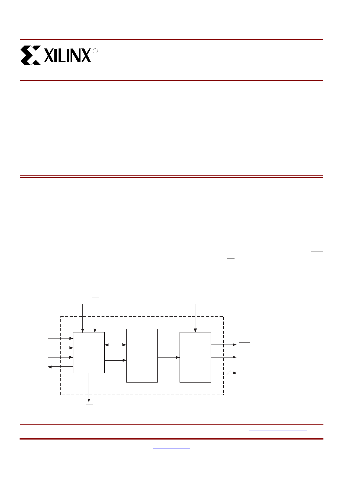
Xilinx introduces the XC18V00 series of in-system programmable configuration PROMs (Figure 1). Initial de vices i n this
3.3V family are a 4-megabit, a 2-megabit, a 1-megabit, a
512-Kbit, and a 256-Kbit PROM that provide an
easy-to-use, cost-effective method for re-programming an d
storing large Xilinx FPGA or CPLD configuration bitstreams.
When the FPGA is in Master Seri al mode, it generates a
configuration clock that dr ives the PROM. A short access
time after the rising CCLK , data is available on the PROM
DATA (D0) pin that is connecte d to the F PGA D
IN
pin. The
FPGA generates the appro priate number of clock pulses to
complete the configuration. When the FPGA is in Slave
Serial mode, the PROM and the FPGA a re clocked by an
external clock.
When the FPGA is in Sl av e-P ara llel or Sele ctMAP Mode , an
external oscillator generates the configuration clock that
drives the PROM and the FPGA. After the rising CCLK
edge, dat a ar e a v ai lab l e on t he PR OM s D ATA (D0-D7) pi n s.
The data is clocked into the F PGA on the following rising
edge of the CCLK. Neither Slave-Parallel nor SelectMAP
utilize a Length Count, so a free-r unning oscillator can be
used.
Multiple devices can be concatenated by using the CEO
output to drive the CE input of the following device. The
clock inputs and the DATA outputs of all PROMs in this
chain are interconnected. All devices are compatible and
can be cascaded with other memb ers of the family or with
the XC17V00 one-time programmable Serial PROM family.
0
XC18V00 Series of In-System
Programmable Configuration
PROMs
DS026 (v3.0) November 12, 2001
00
Product Specification
R
Figure 1: XC18V00 Series Block Diagram
Control
and
JTAG
Interface
Memory
Serial
or
Parallel
Interface
D0 DATA
(Serial or Parallel
[Slave-Parallel/SelectMAP] Mode)
D[1:7]
Slave-Parallel and
SelectMAP Interface
Data
Address
CLK
CE
TCK
TMS
TDI
TDO
OE/Reset
CEO
Data
DS026_01_111201
7
CF
XC18V00 Series of In-System Programmable Configuration PROMs
2 www.xilinx.com DS026 (v3.0) November 12, 2001
1-800-255-7778 Product Specification
R
Pinout and Pin Description
Table 1: Pin Names and Descriptions (pins not listed are “no connect”)
Pin
Name
Boundary
Scan
Order Function Pin Description
44-pin
VQFP
44-pin
PLCC
20-pin
SOIC and
PLCC
D0 4 DATA OUT D0 is the DATA output pin to provide data for
configuring an FPGA in serial mode.
40 2 1
3OUTPUT
ENABLE
D1 6 DATA OUT D0-D7 are the output pins to provide parallel data
for configuring a Xilinx FPGA in
Slave-Parallel/SelectMap mode.
29 35 16
5OUTPUT
ENABLE
D2 2 DATA OUT 42 4 2
1OUTPUT
ENABLE
D3 8 DATA OUT 27 33 15
7OUTPUT
ENABLE
D4 24 DATA OUT 9 15 7
(1)
23 OUTPUT
ENABLE
D5 10 DATA OUT 25 31 14
9OUTPUT
ENABLE
D6 17 DATA OUT 14 20 9
16 OUTPUT
ENABLE
D7 14 DATA OUT 19 25 12
13 OUTPUT
ENABLE
CLK 0 DATA IN Each rising edge on the CLK input increments the
internal address counter if both CE
is Low and
OE/RESET
is High.
43 5 3
OE/
RESET
20 DATA IN When Low, this input holds the address counter
reset and the DATA output is in a high-impedance
state. This is a bidirectional open-drain pin that is
held Low while the PROM is reset. Polarity is NOT
programmable.
13 19 8
19 DATA OUT
18 OUTPUT
ENABLE
CE
15 DATA IN When CE is High, this pin puts the device into
standby mode and resets the address counter. The
DATA output pin is in a high-impedance state, and
the device is in low power standby mode.
15 21 10
XC18V00 Series of In-System Pr ogrammable Configuration PROMs
DS026 (v3.0) November 12, 2001 www.xilinx.com 3
Product Specification 1-800-255-7778
R
CF 22 DATA OUT Allows JTAG CONFIG instructio n to initiate FPGA
configuration without powering down FPGA. This is
an open-drain output that is pulsed Low by the
JTAG CONFIG command.
10 16 7
(1)
21 OUTPUT
ENABLE
CEO
11 DATA OUT Chip Enable Output (CEO) is connected to the CE
input of the next PROM in the chain. This output is
Low when CE
is Low and OE/RESET input is High,
AND the internal address counter has been
incremented beyond its T erminal Count (TC) value.
When OE/RESET
goes Low, CEO stays High until
the PROM is brought out of reset by bringing
OE/RESET
High.
21 27 13
12 OUTPUT
ENABLE
GND GND is the ground connection. 6, 18,
28 &
41
3, 12,
24 &
34
11
TMS MODE
SELECT
The state of TMS on the rising edge of TCK
determines the state transitions at the T est Access
Port (T AP) controller. TMS has an internal 50K ohm
resistive pull-up on it to provide a logic “1” to the
device if the pin is not driven.
511 5
TCK CLOCK This pin is the JTAG test clock. It sequences the
TAP controller and all the JTAG test and
programming electronics.
713 6
TDI DATA IN This pin is the serial input to all JTAG instruction
and data registers. TDI has an internal 50K ohm
resistive pull-up on it to provide a logic “1” to the
system if the pin is not driven.
39 4
TDO DATA OUT This pin is the serial output for all JTAG instruction
and data registers. TDO has an internal 50K ohm
resistive pull-up on it to provide a logic “1” to the
system if the pin is not driven.
31 37 17
V
CC
Positive 3.3V supply voltage for internal logic and
input buffers.
17, 35
& 38
23, 41
& 44
18 & 20
V
CCO
Positive 3.3V or 2.5V supply voltage connected to
the output voltage drivers.
8, 16,
26 &
36
14, 22,
32 &
42
19
Notes:
1. Pin 7 is CF
in Serial Mode, D4 in Slave-Parallel Mode for 20-pin packages.
Table 1: Pin Names and Descriptions (pins not listed are “no connect”) (Continued)
Pin
Name
Boundary
Scan
Order Function Pin Description
44-pin
VQFP
44-pin
PLCC
20-pin
SOIC and
PLCC
XC18V00 Series of In-System Programmable Configuration PROMs
4 www.xilinx.com DS026 (v3.0) November 12, 2001
1-800-255-7778 Product Specification
R
Xilinx FPGAs and Compatible PROMs
Table 2 provides a list of Xilinx FPGAs and compatible
PROMs.
Capacity
In-System Programming
In-System Programmable PROMs can be programmed individually, or two or more can be daisy-chained tog ether and
programmed in-system vi a the standard 4- pin JTAG protocol as shown in Figure 2. In-system programming offers
quick and efficient desig n iterations and el iminates unnecessary package handling or socketing of devices. The Xilinx
development system provides the programming data
sequence using either Xilinx JTAG Programmer software
and a download cable, a third-party JT A G dev elopment system, a JTAG-compatible board tester, or a simple microprocessor interface that emulates the JTAG instruction
sequence. The JTAG Programmer software also outputs
Table 2: Xilinx FPGAs and Compatible PROMs
Device
Configuration
Bits
XC18V00
Solution
XC2V40 360,160 XC18V512
XC2V80 635,360 XC18V01
XC2V250 1,697,248 XC18V02
XC2V500 2,761,952 XC18V04
XC2V1000 4,082,656 XC18V04
XC2V1500 5,659,360 XC18V04
+ XC18V02
XC2V2000 7,492,064 2 of XC18V04
XC2V3000 10,494,432 3 of XC18V04
XC2V4000 15,660,000 4 of XC18V04
XC2V6000 21,849,568 5 of XC18V04
+ XC18V02
XC2V8000 29,063,136 7 of XC18V04
XCV50 559,200 XC18V01
XCV100 781,216 XC18V01
XCV150 1,040,096 XC18V01
XCV200 1,335,840 XC18V02
XCV300 1,751,808 XC18V02
XCV400 2,546,048 XC18V04
XCV600 3,607,968 XC18V04
XCV800 4,715,616 XC18V04 +
XC18V512
XCV1000 6,127,744 XC18V04 +
XC18V02
XCV50E 630,048 XC18V01
XCV100E 863,840 XC18V01
XCV200E 1,442,106 XC18V02
XCV300E 1,875,648 XC18V02
XCV400E 2,693,440 XC18V04
XCV405E 3,430,400 XC18V04
XCV600E 3,961,632 XC18V04
XCV812E 6,519,648 2 of XC18V04
XCV1000E 6,587,520 2 of XC18V04
XCV1600E 8,308,992 2 of XC18V04
XCV2000E 10,159,648 3 of XC18V04
XCV2600E 12,922,336 4 of XC18V04
XCV3200E 16,283,712 4 of XC18V04
XC2S15 197,696 XC18V256
XC2S30 336,768 XC18V512
XC2S50 559,200 XC18V01
XC2S100 781,216 XC18V01
XC2S150 1,040,096 XC18V01
XC2S200 1,335,840 XC18V02
XC2S50E 630,048 XC18V01
XC2S100E 863,840 XC18V01
XC2S150E 1,134,528 XC18V02
XC2S200E 1,442,016 XC18V02
XC2S300E 1,875,648 XC18V02
Devices Configuration Bits
XC18V04 4,194,304
XC18V02 2,097,152
XC18V01 1,048,576
XC18V512 524,288
XC18V256 262,144
Table 2: Xilinx FPGAs and Compatible PROMs
Device
Configuration
Bits
XC18V00
Solution
XC18V00 Series of In-System Pr ogrammable Configuration PROMs
DS026 (v3.0) November 12, 2001 www.xilinx.com 5
Product Specification 1-800-255-7778
R
serial vector format (SVF) files for use with any tools tha t
accept SVF format and with automatic test equipment.
All outputs are held in a high-impedance state or held at
clamp levels during in-system programming.
OE/RESET
The ISP programming algorithm requires issuance of a
reset that causes OE to go Low.
External Programming
Xilinx reprogrammable PROMs can also be programmed by
the Xilinx HW-130 device programmer. This provides the
added flexibility of using pre-pr ogrammed devices in board
design and boundary-scan manufacturing tools, with an
in-system programmable option for future enhancements
and design changes.
Reliability and Endurance
Xilinx in-system p rogrammable product s provide a guaranteed endurance level of 20,000 in-system program/erase
cycles and a minimum data retention of 20 years. Each
device meets all functional, performance, and data retention
specifications within this endurance limit.
Design Security
The Xilinx in-system programmable PROM devices incorporate advanced data security features to fully protect the programming data against unauthorized reading. Table 3
shows the security setting available.
The read security bit ca n be set by the user to prevent the
internal programming pattern from being read or copied via
JTAG. When set, it allows device erase. Erasing the entire
device is the only way to reset the read security bit.
Table 3: Data Security Options
IEEE 1149.1 Boundary-Scan (JTAG)
The XC18V00 family is fully comp liant with the IEEE Std.
1149.1 Boundary-Scan, also known as JTAG. A Test
Access Port (TAP) and registers are pr ovided to s up port all
required boundary scan instructions, as well as many of the
optional instructions specified by IEEE Std. 1149.1. In addition, the JTAG interface is used to implement in-system pro-
gramming (ISP) to facilitate configuration, erasure, and
verification operations on the XC18V00 device.
Table 4 lists the required and optional boundary-scan
instruction s supported in the XC18V 00. Refer to the IEEE
Std. 1149.1 specification for a complete description of
boundary-sc an architecture and the required and optional
instructions.
Default = Reset Set
Read Allowed
Program/Erase Allowed
Read Inhibited via JTAG
Erase Allowed
Figure 2: In-System Programming Operation (a) Solder Device to PCB and (b) Program Using Download Cable
DS026_02_011100
GND
V
CC
(a) (b)
XC18V00 Series of In-System Programmable Configuration PROMs
6 www.xilinx.com DS026 (v3.0) November 12, 2001
1-800-255-7778 Product Specification
R
Instruction Register
The Instruction Register (IR) for the XC18V00 is eight bits
wide and is connected between TDI and TDO during an
instruction scan s equenc e. In pre paration for an inst r uctio n
scan sequence, the instruction register is parallel loaded
with a fixed instruction capture pattern. This pattern is
shifted out onto TDO (LSB first), while an instruction is
shifted into the instr uction register from TDI. The detailed
composition of the in struction capture pat tern is illustrated
in Figure 3.
The ISP Status field, IR(4), contains logic “1” if the device is
currently in ISP m ode; otherwise, it contains log ic “0”. The
Security field, IR(3), contains logic “1” if the device has been
programmed with the security option turned on; otherwise, it
contains logic “0”.
Boundary Scan Register
The boundary -scan registe r is used to cont rol and obser ve
the state of the device pins during the EXTEST, SAMPLE/PRELOAD, and CLAMP instruction s. Each output pin
on the XC18V00 has two regist er stages that cont ribute to
the boundary -scan register, while each input pin o nly has
one register stage.
For each output pin, the register stage neare st to TDI controls and obser ves the output state, and th e second stage
closest to TDO controls and observes the High-Z enable
state of the pin.
For each input pin, the register stage controls and observes
the input state of the pin.
Identification Registers
The IDCODE is a fixed, vendor-assigned value that is use d
to electrically identify the manufacturer and type of the
device being addressed. The IDCODE register is 32 bits
wide. The IDCODE register can be sh ifte d ou t for examination by using the IDCODE instruction. The IDCODE is available to any other system component via JTAG.
The IDCODE register has the following binary format:
vvvv:ffff:ffff:aaaa:aaaa:cccc:cccc:ccc1
where
v = the die version number
f = the family code (50h for XC18V00 family)
a = the ISP PROM product ID (26h for the XC18V04)
c = the company code (49h for Xilinx)
Note: The LSB of the I DCODE register is always read as
logic “1” as defined by IEEE Std. 1149.1
Table 5 lists th e IDCODE register values for the XC18V0 0
devices.
The USERCODE instr uction gives access to a 32-bit user
programmable scratch pad typically used to supply information about the device’s programmed contents. By using th e
USERCODE instruction, a user-programmable identification code can be shifte d out for examination. This code is
loaded into the USERCODE register during programming of
the XC18V00 device. If the device is blank or was not
loaded during programming, the US ERCODE registe r c ontains FFFFFFFFh.
Table 4: Boundary Scan Instructions
Boundary-Scan
Command
Binary
Code [7:0] Description
Required Instructions
BYPASS 11111111 Enab l es BYPASS
SAMPLE/
PRELOAD
00000001 Enables boundary-scan
SAMPLE/PRELOAD operation
EXTEST 00000000 Enabl es bou ndary-scan
EXTEST operation
Optional Instructions
CLAMP 11111010 Enables boundary-scan
CLAMP operation
HIGHZ 11111100 all outputs in high-impedance
state simultaneously
IDCODE 11111110 Enables shifting out
32-bit IDCODE
USERCODE 11111101 Enables shifting out
32-bit USERCODE
XC18V00 Specific Instructions
CONFIG 11101110 Initiates FPGA configuration
by pulsing CF
pin Low
IR[7:5] IR[4] IR[3] IR[2] IR[1:0]
TDI-> 0 0 0 ISP
Status
Security 0 0 1 ->TD
O
Notes:
1. IR(1:0) = 01 is specified by IEEE Std. 1149.1
Figure 3: Instruction Register Values Loaded into IR as
Part of an Instruction Scan Sequence
Table 5: IDCODES Assigned to XC18V00 Devices
ISP-PROM IDCODE
XC18V01 05024093h
XC18V02 05025093h
XC18V04 05026093h
XC18V256 05022093h
XC18V512 05023093h

XC18V00 Series of In-System Pr ogrammable Configuration PROMs
DS026 (v3.0) November 12, 2001 www.xilinx.com 7
Product Specification 1-800-255-7778
R
XC18V00 TAP Characteristics
The XC18V00 family performs both in-system programming
and IEEE 1149.1 boundary-scan (JTA G) testing via a single
4-wire Test Access Port (TAP). This simplifies system
designs and allows standard Automatic Test Equipment to
perform both functions. The AC characteristics of the
XC18V00 TAP ar e desc r ib ed as follows.
TAP Timing
Figure 4 shows the timing relationsh ips of th e TAP signals.
These TAP timing characteristics are identical for both
boundary-scan and ISP operations.
TAP AC Parameters
Table 6 shows the timing parameters for the TAP waveforms shown in Figure 4
Connecting Configuration PROMs
Connecting the FPGA device with the configurati on PROM
(see Figure 6).
• The DATA output(s) of the PROM(s) drives the D
IN
input of the lead FPGA device.
• The Master FPGA CCLK output drives the CLK input(s)
of the PROM(s) (in Master Serial mode only).
• The CEO
output of a PROM drives the CE in put of the
next PROM in a daisy chain (if any).
• The OE/RESET
input of all PROMs is best driven by
the INIT
output of the lead FPGA device. This
connection assur es that th e PROM address counter is
reset before the start of any (re)configuration, even
when a reconfiguration is initiated by a V
CC
glitch.
• The PROM CE
input can be driven from the DONE pin.
The CE
input of the first (or only) PROM can be dr iven
by the DONE output of the first FPGA device, provided
that DONE is not per manently grounded. CE
can also
be permanently tied Low, but this keeps the DATA
output active and causes an unnecessary supply
current of 10 mA maximum.
• Slave-Parallel/SelectMap mode is similar to slave serial
mode. The DATA is clocked out of th e PROM one byte
per CCLK instead of one bi t per CCL K cycle. See FPGA
data sheets for special configur a t ion r equi r em ents.
Figure 4: Test Access Port Timing
Table 6: Test Access Port Timing Parameters
Symbol Parameter Min Max Units
T
CKMIN1
TCK minimum clock period 100 - ns
T
CKMIN2
TCK minimum clock period, Bypass Mode 50 - ns
T
MSS
TMS setup time 10 - ns
T
MSH
TMS hold time 25 - ns
T
DIS
TDI setup time 10 - ns
T
DIH
TDI hold time 25 - ns
T
DOV
TDO valid delay - 25 ns
TCK
T
CKMIN
T
MSS
TMS
TDI
TDO
T
MSH
T
DIH
T
DOV
T
DIS
DS026_04_020300

XC18V00 Series of In-System Programmable Configuration PROMs
8 www.xilinx.com DS026 (v3.0) November 12, 2001
1-800-255-7778 Product Specification
R
Initiating FPGA Configuration
The XC18V00 devices incorporat e a pin named CF t hat is
controllable through the JTAG CONFIG instr uct ion . E xecuting the CONFIG instruction through JT AG pulses the CF
low
for 300-500 ns, which resets the FPGA and initiates configuration.
The CF
pin must be connected to the PROGRAM pin on the
FPGA(s) to use this feature.
The JTAG Programmer software can also issue a JTAG
CONFIG command to initiate FPGA configuration through
the “Load FPGA” setting.
Selecting Configuration Modes
The XC18V00 accommoda tes serial and parallel methods
of configuration. The configuration modes are selectable
through a user control register in the XC18V00 device. This
control register is accessible through JTAG, and is set using
the “Parallel mode” setting o n the Xili nx JTAG Programmer
software. Serial output is the default programming mode.
Master Serial Mode Summary
The I/O and logic functions of the Con figurable Logi c Block
(CLB) and their associated interconnections are established
by a configuration program. The program is loa ded either
automatically upon power up, or on command, depend ing
on the state of the three FPG A mo de p ins. In M aster Se rial
mode, the FPGA automatic ally lo ads th e con figuration program from an external memory . Xilinx PROMs are designed
to accommodate the Master Serial mod e.
Upon power- up or reconfi gur atio n, an F PGA ent ers the Ma ster Serial mode when ever all three of the FPGA mo de -sel ect
pins are Low (M0=0, M1=0, M2=0). Data is read from the
PROM sequentially on a si ngle da ta line. Sync hron izati on is
provided by the rising ed ge of the temporary sign al CCLK,
which is generated by the FPGA during configuration.
Master Serial Mod e provides a simple configuration interface. Only a serial data line, a cl ock line, and two control
lines are required to configure an FPGA. Data from the
PROM is read sequentially, accessed via the internal
address and bit counte rs which are incremented on every
valid rising edge of CCLK. If the user-programmable,
dual-function D
IN
pin on the FPGA i s u se d on ly for config u-
ration, it must still be hel d at a defined level during nor mal
operation. The Xilinx FPGA families take care of this automatically with an on-chip pull-up resistor.
Cascading Configuration PROMs
For multiple FPGAs configured as a serial daisy-chain, or a
single FPGA requi ring larger configuration memor ies in a
serial or SelectMAP configuration mode, cascaded PROMs
provide additional memory (Figure 5). Multiple XC18V00
devices can be concatenated by using the CEO
output to
drive the CE
input of the downstream device. The clock
inputs and the dat a outputs of all XC18V 00 devices in the
chain are interconnected. After the last bit from the first
PROM is read, the next clock signal to the PROM asserts its
CEO
output Low and drives its DATA line to a high -impedance state. The second PROM recognizes the Low level on
its CE
input and enables its DATA output. See Figure 6.
After configuration is complete, address counters of all cascaded PROMs are reset if the PROM OE/R ESET
pin goes
Low .

XC18V00 Series of In-System Pr ogrammable Configuration PROMs
DS026 (v3.0) November 12, 2001 www.xilinx.com 9
Product Specification 1-800-255-7778
R
Figure 5: JTAG Chain for Configuring Devices in Master Serial Mode
4.7K
4.7K
**
1
2
3
4
TDO
DOUT
TDI
TMS
TCK
Vcc
Vcc
DIN
CCLK
DONE
INIT
Vcc MODE PINS*
Xilinx
FPGA
Master
Serial
Vcc D0
Vcco
TDI CLK
TMS CE
TCK CEO
OE/RESET
PROGRAM
TDO
TDI
TMS
TCK
DIN
CCLK
DONE
INIT
Vcc MODE PINS*
Xilinx
FPGA
Slave
Serial
PROGRAMCF
TDO
GND
* For Mode pin connections, refer to appropriate FPGA data sheet.
** Virtex, Virtex-E is 300 ohms, all others are 4.7K.
XC18V00
Cascaded
PROM
TDI
TMS
TCK
TDO
J1
DS026_08_011501
VccVccoVcco
Vcc
D0
Vcco
TDI CLK
TMS CE
TCK CEO
OE/RESET
CF
TDO
GND
XC18V00
First
PROM
Vcc

XC18V00 Series of In-System Programmable Configuration PROMs
10 www.xilinx.com DS026 (v3.0) November 12, 2001
1-800-255-7778 Product Specification
R
Figure 6: (a) Master Serial Mode (b) Virtex SelectMAP Mode (c) Spartan-II/IIE Slave-Parallel Mode
(dotted lines indicate optional connection)
PROGRAM
DIN
CCLK
INIT
DONE
First
PROM
DATA
CEO
CLK
CE
OPTIONAL
Slave FPGAs
with identical
configurations
Vcc
FPGA
(Low Resets the Address Pointer)
VCCV
CCO
OPTIONAL
Daisy-chained
FPGAs with
different
configurations
OE/RESET
DOUT
Modes
Vcco
CF
PROGRAM
VIRTEX
Select MAP
BUSY
CS
WRITE
INIT
D[0:7]
CCLK
DONE
Virtex SelectMAP Mode
CE
Modes
NC
3.3V
External
Osc
V
CC
4.7K
V
CC
**
V
CC
3.3K
V
CC
3.3K
V
CC
1K
I/O
M0
M1
CS
PROGRAM
Spartan-II,
Spartan- IIE
DONE
INIT
XC18Vxx
CEO
CE
OE/RESET
Spartan-II/IIE Slave-Parallel Mode
Master Serial Mode
8
CF
CLK
D[0:7]
D[0:7]
CCLK
M0
M1
CS
PROGRAM
Optional
Daisy-chained
Spartan-II,
Spartan-IIE
DOUT
DONE
INIT
D[0:7]
CCLK
8
To Additional
Optional
Daisy-chained
Devices
To Additional
Optional
Daisy-chained
Devices
External Osc
I/O
1K
(1) CS and WRITE must be pulled down to be used as I/O. One option is shown.
(2) Virtex, Virtex-E is 300 ohms, all others are 4.7K.
(3) For Mode pin connections, refer to the appropriate FPGA data sheet.
(4) External oscillator required for Virtex/E SelectMAP or Virtex-II Slave SelectMAP modes.
DS026_05_111201
(1) For Mode pin connections, refer to the appropriate FPGA data sheet.
(2) Virtex is 300 ohms.
Cascaded
PROM
DATA
CLK
CE
OE/RESET
CF
CLK
D[0:7]
OE/RESET
XC18Vxx
CF
CEO
V
CCVCCO
VCCV
CCO
V
CCO
VCCV
CCO
V
CC
CS(0)
V
CC
(2)
(1)
4.7K
(1)
(1)
(2)
(4)
CE
4.7K
V
CC
V
CC
3.3K
CLK
D[0:7]
OE/RESET
XC18Vxx
CF
CEO
V
CCVCCO
VCCV
CCO
V
CC
CS(1)
V
CC

XC18V00 Series of In-System Pr ogrammable Configuration PROMs
DS026 (v3.0) November 12, 2001 www.xilinx.com 11
Product Specification 1-800-255-7778
R
5V Tole r ant I/Os
The I/Os on each re- programmable PROM are fully 5V to lerant even through the core power supply is 3.3V. This
allows 5V CMOS signals to connec t directly to the PROM
inputs without damage. In addition, the 3.3V V
CC
power
supply can be applied before or after 5V signals are applied
to the I/Os. In mixed 5V/3.3V/2.5V systems, the user pins,
the core power supply (V
CC
), and the output power supply
(V
CCO
) can have power applied in any order. This makes
the PROM devices immune to power supply sequencing
issues.
Reset Activation
On power up, OE/RESET is held low until the X C18V00 is
active (1 ms) and able to supply data after receiving a CCLK
pulse from the FPGA. OE/RESET
is connected to an exter-
nal resistor to pull OE/RESET
HIGH releasing the FPGA
INIT
and allowing configuration to begin. OE/RESET is held
low until the XC18V00 voltage reac hes the operating voltage range. If the power drops below 2.0V , the PROM resets.
OE/RESET
polarity is NOT programmable.
Standby Mode
The PRO M ente rs a l ow- po we r stan db y mode when e v er C E
is asser ted High. The outpu t remains in a high-imp edance
state regardless of the state of the OE input. JTAG pins
TMS, TDI and TDO can b e in a high-impedance state or
High.
Customer Control Pins
The XC18V00 PROMs have various control bits accessible
by the customer. These can be set after the array has been
programmed using “Skip User Array” in Xilinx JTAG Pro-
grammer Software.
Table 7: Truth Table for PROM Control Inputs
Control Inputs
Internal Address
Outputs
OE/RESET CE DATA CEO I
CC
High Low If address < TC
(1)
: increment
If address > TC
(1)
: don’t change
Active
High-Z
High
Low
Active
Reduced
Low Low Held reset High-Z High Active
High High Held reset High-Z High Standby
Low High Held reset High-Z High Standby
Notes:
1. TC = Terminal Count = highest address value. TC + 1 = address 0.

XC18V00 Series of In-System Programmable Configuration PROMs
12 www.xilinx.com DS026 (v3.0) November 12, 2001
1-800-255-7778 Product Specification
R
Absolute Maximum Ratings
(1,2)
Recommended Operating Conditions
Quality and Reliability Characteristics
Symbol Description Value Units
V
CC
Supply voltage relative to GND –0.5 to +4.0 V
V
IN
Input voltage with respect to GND –0.5 to +5.5 V
V
TS
Voltage applied to High-Z output –0.5 to +5.5 V
T
STG
Storage temperature (ambient) –65 to +150
p
C
T
SOL
Maximum soldering temperature (10s @ 1/16 in.) +260
p
C
T
J
Junction temperature +150
p
C
Notes:
1. Maximum DC undershoot below GND mu st be limited to either 0.5 V or 10 mA, whiche ver is easie r to achiev e. During t ransitions , the
device pins can undershoot to –2.0V or overshoot to +7.0V, provided this over- or undershoot lasts less then 10 ns and with the
forcing current being limited to 200 mA.
2. Stresses beyond those listed under Absolute Maximum Ratings might cause permanent damage to the device. These are stress
ratings only, and functional operation of the device at these or any other conditions beyond those li st ed un der Operating Con di tions
is not implied. Exposure to Absolute Maximum Ratings conditions for extended periods of time might affect device reliability.
Symbol Parameter Min Max Units
V
CCINT
Internal voltage supply (TA = 0pC to +70pC) Commercial 3.0 3.6 V
Internal voltage supply (T
A
= –40pC to +85pC) Industrial 3.0 3.6 V
V
CCO
Supply voltage for output drivers for 3.3V operation 3.0 3.6 V
Supply voltage for output drivers for 2.5V operation 2.3 2.7 V
V
IL
Low-level input voltage 0 0.8 V
V
IH
High-level input voltage 2.0 5.5 V
V
O
Output voltage 0 V
CCO
V
T
VCC
VCC rise time from 0V to nominal voltage
(1)
150ms
Notes:
1. At power up , the de vic e requires the V
CC
power supply t o monoton ically rise from 0V to no minal v olta ge withi n the spec ified VCC rise
time. If the power supply cannot meet this requirement, then the device might not perform power-on-reset properly.
Symbol Description Min Max Units
T
DR
Data retention 20 - Years
N
PE
Program/erase cycles (Endurance) 20,000 - Cycles
V
ESD
Electrostatic discharge (ESD) 2,000 - Volts

XC18V00 Series of In-System Pr ogrammable Configuration PROMs
DS026 (v3.0) November 12, 2001 www.xilinx.com 13
Product Specification 1-800-255-7778
R
DC Characteristics Over Operating Conditions
Symbol Parameter Tes t Conditions Min Max Units
V
OH
High-level output voltage for 3.3V outputs IOH = –4 mA 2.4 - V
High-level output voltage for 2.5V outputs I
OH
= –500 NA 90% V
CCO
-V
V
OL
Low-level output voltage for 3.3V outputs IOL = 8 mA - 0.4 V
Low-level output voltage for 2.5V outputs IOL = 500 NA-0.4V
I
CC
Supply current, active mode 25 MHz - 25 mA
I
CCS
Supply current, standby mode - 10 mA
I
ILJ
JTAG pins TMS, TDI, and TDO V
CC =
MAX
V
IN
= GND
–100 -
N
A
I
IL
Input leakage current V
CC
= Max
V
IN
= GND or V
CC
–10 10
N
A
I
IH
Input and output High-Z leakage current V
CC
= Max
V
IN
= GND or V
CC
–10 10
N
A
C
IN
and
C
OUT
Input and output capacitance VIN = GND
f = 1.0 MHz
-10pF
Notes:
1. 18V01/18V512/18V256 only, cascadable.
2. 18V01/18V512/18V256 only, non-cascadable, no brown-out protection.

XC18V00 Series of In-System Programmable Configuration PROMs
14 www.xilinx.com DS026 (v3.0) November 12, 2001
1-800-255-7778 Product Specification
R
AC Characteristics Over Operating Conditions for XC18V04 and XC18V02
OE/RESET
CE
CLK
DATA
T
CE
T
OE
T
LC
T
SCE
T
HCE
T
HOE
T
CAC
T
OH
T
DF
T
OH
T
HC
DS026_06_012000
T
CYC
Symbol Description Min Max Units
T
OE
OE/RESET to data delay - 10 ns
T
CE
CE to data delay - 20 ns
T
CAC
CLK to data delay - 20 ns
T
OH
Data hold from CE, OE/RESET, or CLK 0 - ns
T
DF
CE or OE/RESET to data float delay
(2)
-25ns
T
CYC
Clock periods 50 - ns
T
LC
CLK Low time
(3)
10 - ns
T
HC
CLK High time
(3)
10 - ns
T
SCE
CE setup time to CLK (to guarantee proper counting)
(3)
25 - ns
T
HCE
CE High time (to guarantee proper counting) 2 -
N
s
T
HOE
OE/RESET hold time (guarantees counters are reset) 25 - ns
Notes:
1. AC test load = 50 pF.
2. Float delays are measured with 5 pF AC loads. Transition is measured at ±200 mV from steady state active levels.
3. Guaranteed by design, not tested.
4. All AC parameters are measured with V
IL
= 0.0V and VIH = 3.0V.
5. If T
HCE
High < 2 Ns, TCE = 2 Ns.

XC18V00 Series of In-System Pr ogrammable Configuration PROMs
DS026 (v3.0) November 12, 2001 www.xilinx.com 15
Product Specification 1-800-255-7778
R
AC Characteristics Over Operating Conditions for XC18V01, XC18V512, and
XC18V256
OE/RESET
CE
CLK
DATA
T
CE
T
OE
T
LC
T
SCE
T
HCE
T
HOE
T
CAC
T
OH
T
DF
T
OH
T
HC
DS026_06_012000
T
CYC
Symbol Description Min Max Units
T
OE
OE/RESET to data delay - 10 ns
T
CE
CE to data delay - 15 ns
T
CAC
CLK to data delay - 15 ns
T
OH
Data hold from CE, OE/RESET, or CLK 0 - ns
T
DF
CE or OE/RESET to data float delay
(2)
-25ns
T
CYC
Clock periods 30 - ns
T
LC
CLK Low time
(3)
10 - ns
T
HC
CLK High time
(3)
10 - ns
T
SCE
CE setup time to CLK (to guarantee proper counting)
(3)
20 - ns
T
HCE
CE hold time to CLK (to guarantee proper counting) 2 -
N
s
T
HOE
OE/RESET hold time (guarantees counters are reset) 20 - ns
Notes:
1. AC test load = 50 pF.
2. Float delays are measured with 5 pF AC loads. Transition is measured at ±200 mV from steady state active levels.
3. Guaranteed by design, not tested.
4. All AC parameters are measured with V
IL
= 0.0V and VIH = 3.0V.
5. If T
HCE
High < 2 Ns, TCE = 2 Ns.

XC18V00 Series of In-System Programmable Configuration PROMs
16 www.xilinx.com DS026 (v3.0) November 12, 2001
1-800-255-7778 Product Specification
R
AC Characteri stics Over Operating Conditions When Cascading f or XC18V0 4 and
XC18V02
CLK
DATA
CE
CEO
First Bit
Last Bit
T
CDF
DS026_07_020300
OE/RESET
T
OCK
T
OOE
T
OCE
Symbol Description Min Max Units
T
CDF
CLK to data float delay
(2,3)
-25 ns
T
OCK
CLK to CEO delay
(3)
-20 ns
T
OCE
CE to CEO delay
(3)
-20 ns
T
OOE
OE/RESET to CEO delay
(3)
-20 ns
Notes:
1. AC test load = 50 pF.
2. Float delays are measured with 5 pF AC loads. Transition is measured at ±200 mV from steady state active levels.
3. Guaranteed by design, not tested.
4. All AC parameters are measured with VIL = 0.0V and VIH = 3.0V.

XC18V00 Series of In-System Pr ogrammable Configuration PROMs
DS026 (v3.0) November 12, 2001 www.xilinx.com 17
Product Specification 1-800-255-7778
R
AC Character istics Over Operating Conditions When Cascading for XC18V01,
XC18V512, and XC18V256
CLK
DATA
CE
CEO
First Bit
Last Bit
T
CDF
DS026_07_020300
OE/RESET
T
OCK
T
OOE
T
OCE
Symbol Description Min Max Units
T
CDF
CLK to data float delay
(2,3)
-25 ns
T
OCK
CLK to CEO delay
(3)
-20 ns
T
OCE
CE to CEO delay
(3)
-20 ns
T
OOE
OE/RESET to CEO delay
(3)
-20 ns
Notes:
1. AC test load = 50 pF.
2. Float delays are measured with 5 pF AC loads. Transition is measured at ±200 mV from steady state active levels.
3. Guaranteed by design, not tested.
4. All AC parameters are measured with VIL = 0.0V and VIH = 3.0V.

XC18V00 Series of In-System Programmable Configuration PROMs
18 www.xilinx.com DS026 (v3.0) November 12, 2001
1-800-255-7778 Product Specification
R
Ordering Information
Valid Ordering Combinations
Marking Information
XC18V04VQ44C XC18V02VQ44C XC18V01VQ44C XC18V512VQ44C XC18V256VQ44C
XC18V04PC44C XC18V02PC44C XC18V01PC20C XC18V512PC20C XC18V256PC20C
XC18V01SO20C XC18V512SO20C XC18V256SO20C
XC18V04VQ44I XC18V02VQ44I XC18V01VQ44I XC18V512VQ44I XC18V256VQ44I
XC18V04PC44I XC18V02PC44I XC18V01PC20I XC18V512PC20I XC18V256PC20I
XC18V01SO20I XC18V512SO20I XC18V256SO20I
XC18V04 VQ44 C
Operating Range/Processing
C=Commercial (T
A =
0p to +70pC)
I = Industrial (T
A
= –40p to +85pC)
Package Type
VQ44 = 44-pin Plastic Quad Flat Package
PC44 = 44-pin Plastic Chip Carrier
(1)
SO20 = 20-pin Small-Outline Package
(2)
PC20 = 20-pin Plastic Leaded Chip Carrier
(2)
Device Number
XC18V04
XC18V02
XC18V01
XC18V512
XC18V256
Notes:
1. XC18V04 and XC18V02 only.
2. XC18V01, XC18V512, and XC18V256 only.
20-pin Package
(1)
Due to the small size of the commercial serial PROM packages, the complete ordering par t number cannot be
marked on the package. The XC prefix is deleted and the package code is simplified. Device marking is as follows:
44-pin Package
XC18V04 VQ44 C
Operating Range/Processing
C=Commercial (T
A =
0p to +70pC)
I = Industrial (T
A
= –40p to +85pC)
Package Type
VQ44 = 44-pin Plastic Quad Flat Package
PC44 = 44-pin Plastic Leaded Chip Carrier
(1)
Notes:
1. XC18V02 and XC18V04 Only.
Device Number
XC18V04
XC18V02
XC18V01
XC18V512
XC18V256
18V01 S C
Operating Range/Processing
C = Commercial (T
A =
0p to +70pC)
I = Industrial (T
A
= –40p to +85pC)
Package Type
S20 = 20-pin Small-Outline Package
J20 = 20-pin Plastic Leaded Chip Carrier
Device Number
18V01
18V512
18V256
Notes:
1. XC18V01, XC18V512, and XC18V256 only.

XC18V00 Series of In-System Pr ogrammable Configuration PROMs
DS026 (v3.0) November 12, 2001 www.xilinx.com 19
Product Specification 1-800-255-7778
R
Revision History
The following table shows the revision history for this document.
Date Version Revision
2/9/99 1.0 First publication of this early access specification
8/23/99 1.1 Edited text, changed marking, added CF
and parallel load
9/1/99 1.2 Corrected JTAG order, Security and Endurance data.
9/16/99 1.3 Corrected SelectMAP diagram, control inputs, reset polarity. Added JTAG and CF
description, 256 Kbit and 128 Kbit devices.
01/20/00 2.0 Added Q44 Package, changed XC18xx to XC18Vxx
02/18/00 2.1 Updated JTAG configuration, AC and DC characteristics
04/04/00 2.2 Removed stand alone resistor on INIT pin in Figure 5. Added Virtex-E and EM parts to
FPGA table.
06/29/00 2.3 Removed XC18V128 and updated format. Added AC characteristics for XC18V01,
XC18V512, and XC18V256 den si tie s.
11/13/00 2.4 Features: changed 264 MHz to 264 Mb/s at 33 MHz; AC Spec.: T
SCE
units to ns, T
HCE
CE High time units to Ns. Removed Standby Mode statement: “The lower power standby
modes available on some XC18V00 devices are set by the user in the programming
software”. Changed 10,000 cycles endurance to 20,000 cycles.
01/15/01 2.5 Updated Figures 5 and 6, added 4.7 resistors. Identification registers: changes ISP
PROM product ID from 06h to 26h.
04/04/01 2.6 Updated Figure 6, Virtex SelectMAP mode; added XC2V products to Compatible PROM
table; changed Endurance from 10,000 cycles, 10 years to 20,000, 20 years;
04/30/01 2.7 Updated Figure 6: removed Virtex-E in Note 2, fixed SelectMAP mode connections.
Under AC Characteristics Over Operating Conditions for XC18V04 and XC18V02,
changed T
SCE
from 25 ms to 25 ns.
06/11/01 2.8 AC Characteristics Over Operating Conditions for XC18V01, XC18V512, and XC18V256
Changed Min values for T
SCE
from 20 ms to 20 ns and for T
HCE
from 2 ms to 2 Ns.
09/28/01 2.9 Changed the boundary scan order for the CEO pin in Table 1, updated the configuration
bits values in the table under Xilinx FPGAs and Compatible PROMs, and added
information to the Recom men ded Op erating Cond iti ons table.
11/12/01 3.0 Updated for Spartan-IIE FPGA family.
 Loading...