

Page 1
0
R
DS073 (v1.0) July 26, 2000
08
Features
• One-time programmable (OTP) read-only memory
designe d to sto re c on f ig ur ation bitstr ea m s o f X ilinx
FPGA devices
• Simple interface to the FPGA; configurable to use a
one user I/O pin
• Cascadable for storing longer or multiple bitstreams
• Programmable reset polarity (active High or active
Low) for compatibilit y with d iffe re nt FP GA solution s
• Supports fast configuration
• Low-power CMOS Floating Gate process
• 3.3V supply voltage
• Available in compact plastic packages: VQ44, PC44,
PC20, VO8, and SO20
• Programming support by leading programmer
manufacturers.
• Design support using the Xilin x Alli anc e and
Foundation series software packages.
• Dual configuration modes for the XC17V16 and
XC17V08
- Serial slow/fast configuration (up to 33 MHz)
- Parallel (up to 264 MHz)
• Guaranteed 20 year life data retention
XC17V00 Series Configuration
PROM
Advance Product Specification
Description
Xilinx introduces the high-density XC17V00 family of configuration PROMs which provide an easy-to-use, cost-effective method for storing large Xilinx FPGA configuration
bitstreams. Initial devices in the 3.3V family are available in
16 Mb, 8 Mb, 4 Mb, 2 Mb, and 1 Mb densities.
When the FPGA is in Master Serial mode, it generates a
configuration clock that drives the PROM. A short access
time after the rising clock edge, data appears on the PROM
DATA out put pin that is connected to the FPGA DIN pin. The
FPGA generates the appropriate num ber of clock pulses to
complete the configuration. Once configured, it disables the
PROM. When the FPGA is in Slave Serial mode, the PROM
and the FPGA must both be clocked by an incoming signal.
When the FPGA is in SelectMAP mode, an external oscillator will generate the configuration clock that drives the
PROM and the FPGA. After the rising CCLK edge, data are
available on the P ROMs DATA (D0-D7) pins. The data will
be clocked into the FPGA on the following rising edge of the
CCLK. SelectMAP does not utilize a Length Count, so a
free-running oscillator may be used. See Figure 3.
Multiple devices can be concatenated by using the CEO
output to drive the CE input of the following device. The
clock inputs and the DATA outputs of all PROMs in this
chain are interconnected. All devices are compatible and
can be cascaded with other members of the family.
For device programming, either the Xilinx Alliance or Foundation series development system compiles the FPGA
design file into a standard He x format, which is then t ransferred to most commercial PROM programmers.
© 2000 Xilinx, Inc. All rights reserved. All Xilinx trademarks, registered trademarks, patents, and disclaimers are as listed at http://www.xilinx.com/legal.htm.
All other trademarks and registered trademarks are the property of their respective owners. All specifications are subject to change without notice.
DS073 (v1.0) July 26, 2000 www.xilinx.com 1
Advance Product Specifi cation 1-800-255-7778
Page 2
XC17V00 Series Configuration PR OM
R
RESET/
OE
or
OE/
RESET
CE
CLK
V
CC
V
PP
GND
CEO
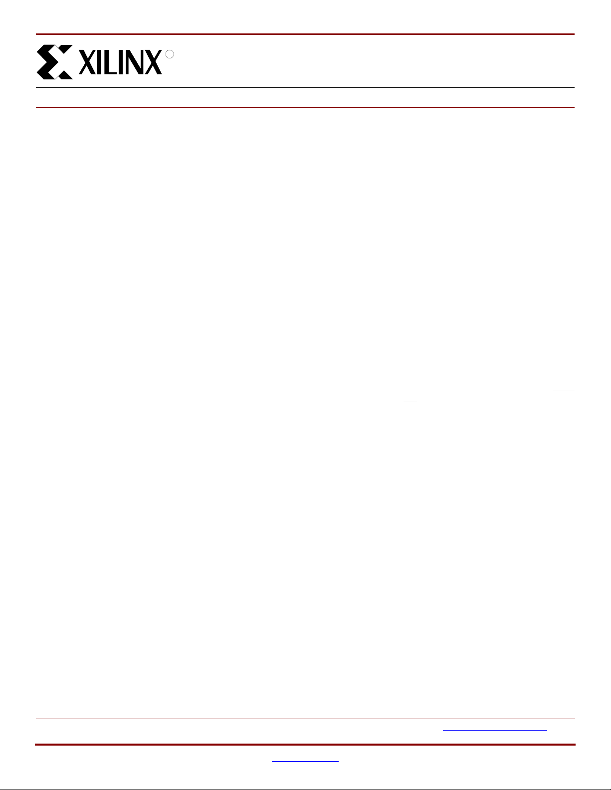
Address Counter
EPROM
Cell
TC
Output
OE
DATA
Matrix
DS073_01_072600
Figure 1: Simplified Block Diagram for XC17V04, XC17V02, and XC17V01 (does not show programming circuit)
RESET/
OE
or
OE/
RESET
CE
CLK
BUSY
V
CC
V
PP
GND
CEO
Address Counter
EPROM
Cell
Matrix
TC
Output
8
OE
D0 Data
(Serial or Parallel Mode)
77
D[1:7]
(SelectMAP Interface)
DS073_02_072600
Figure 2: Simplified Block Diagram for XC17V16 and XC 17V08 (does not show programming circuit)
2 www.xilinx.com DS073 (v1.0) July 26, 2000
1-800-255-7778 Advance Product Specification
Page 3
R
XC17V00 Series Configuration PR OM
Pin Description
DATA[0:7]
Data output is in a high-impedance state when either CE or
OE
are inactive. During programming, the D0 pin is I/O.
Note that OE
active Low.
Note: XC17V04, XC17V02, and XC17V01 have serial output
only.
CLK
Each rising edge on the CLK input increments the internal
address counter, if both CE
RESET/OE
When High, this input hol ds the ad dress counter res et and
puts the DATA output in a high-impedance state. The polarity of this input pin is programmable as either RESET/OE
OE/RESET
the pin as RESET/OE
sible on all devices. When RESET is active, the address
counter is held at "0", and puts the DATA output in a
high-impedance state. The polarity of this input is programmable. The default is ac tive High RE SET, but the preferred
option is active Low RESET
FPGAs INIT
The polarity of this pin is controlled in the programmer interface. This input pin is easily inverted using the Xilinx
HW-130 Programmer. Third-party programmers have different methods to invert this pin.
CE
When High, this pin disables the internal address counter,
puts the DATA output in a high-impedance state, and forces
the device into low-I
can be programmed to be either active High or
and OE are ac tive .
or
. To avoid confusion, this document describes
, although the opposite polarity is pos-
, because it can be driven by the
pin.
standby mode.
CC
BUSY (XC17V16 and XC17V08 only)
If BUSY pin is floating, the user must program the BUSY bit
which will cause BUSY pin to go Low internally. When
asserted High, output data are held and when BUSY pin
goes Low, data output will resume.
V
PP
Programming voltage. No overshoot above the specified
max voltage is permitted on this pin. For normal read operation, this pin must be connected to V
may lead to unpredictable, temperature-dependent operation and severe problems in circuit debugging. Do not leave
V
floating!
PP
. Failure to do so
CC
VCC and GND
Positive supply and ground pins.
PROM Pinouts for XC17V16 and XC17V08
Pin Name 44-pin VQFP 44-pin PLCC
BUSY 24 30
D0 40 2
D1 29 35
D2 42 4
D3 27 33
D4 9 15
D5 25 31
D6 14 20
D7 19 25
CLK 43 5
CEO
Chip Enable output, to be connected t o the CE input of t he
next PROM in the daisy chain. This output is Low when the
CE
and OE inputs are both active AND the internal address
counter has been increment ed beyond its Terminal Count
(TC) value. In other words: when the PROM has been read,
CEO
will follow C E as long as OE is act i v e . W h en OE goes
inactive, CE O
OE
can be programmed t o be either active High or active
Low.
stays High until the PROM is reset. Note that
RESET/OE
(OE/RESET)
CE
GND 6, 18, 28, 27, 41 3, 12, 24, 34, 43
CEO
V
PP
V
CC
8, 16, 17, 26, 36, 3814, 22, 23, 32,
13 19
15 21
21 27
35 41
42, 44
Capacity
Devices Configuration Bits
XC17V16 16,777,216
XC17V08 8,388,608
DS073 (v1.0) July 26, 2000 www.xilinx.com 3
Advance Product Specifi cation 1-800-255-7778
Page 4
XC17V00 Series Configuration PR OM
R
PROM Pinouts for XC17V04, XC17V02, and XC17V01
8-pin
Pin Name
VOIC
DATA 112402
CLK 2 3 4 43 5
RESET/OE
(OE/RESET)
CE
GND 5 11 10 18, 41 24, 3
CEO
V
PP
V
CC
20-pin
SOIC
20-pin
PLCC
44-pin
VQFP
44-pin
PLCC
38 6 1319
410 8 15 21
61314 2127
71817 35 41
82020 38 44
Capacity
Devices Configuration Bits
XC17V04 4,194,304
XC17V02 2,701,312
XC17V01 1,679,360
Xilinx FPGAs and Compatible PROMs
Configuration
Device
XCV50 559,200 XC17V01
XCV100 781,216 XC17V01
XCV150 1,040,096 XC17V01
XCV200 1,335,840 XC17V01
XCV300 1,751,808 XC17V02
XCV400 2,546,048 XC17V02
XCV600 3,607,968 XC17V04
XCV800 4,715,616 XC17V08
XCV1000 6,127,744 XC17V08
XCV50E 630,048 XC17V01
XCV100E 863,840 XC17V01
XCV200E 1,442,106 XC17V01
XCV300E 1,875,648 XC17V02
XCV400E 2,693,440 XC17V02
Bits PROM
Xilinx FPGAs and Compatible PROMs
Configuration
Device
Bits PROM
XCV600E 3,961,632 XC17V04
XCV812E 6,519,648 XC17V08
XCV1000E 6,587,520 XC17V08
XCV1600E 8,308,992 XC17V08
XCV2000E 10,159,648 XC17V16
XCV2600E 12,922,336 XC17V16
XCV3200E 16,283,712 XC17V16
Notes:
1. The sugges ted PROM is determined by compat ibility wi th the
higher configuration frequency of the Xil inx FPGA CCLK.
Controlling PROMs
Connecting the FPGA device with the PROM.
• The DATA output(s) of the of the PROM(s) drives the
input of the lead FPGA device.
D
IN
• The Master FPGA CCLK output drives the CLK input(s)
of the PROM(s).
• The CEO
next PROM in a daisy chain (if any).
• The RESET
the INIT
connection assures that the PROM address counter is
reset before the start of any (re)configuration, even
when a reconfiguration is initiated by a V
Other methods—such as d riving RESET
or system reset—assume the PROM internal
power-on-reset is always in step with the FPGA’s
internal power-on-reset. This may not be a safe
assumption.
• The PROM CE
or DONE pins. Using LDC avoids potential contention
on the D
• The CE
the DONE output of the lead FPGA device, provided
that DONE is not permanently grounded. Otherwise,
LDC
unconditionally High during user operation. CE
also be permanent ly tied Low, but this keeps the DATA
output active and causes an unnecessary supply
current of 10 mA maximum.
• SelectMA P mode is similar to Slave Serial mode. The
DATA is clocked out of the PROM one byte p er CCLK
instead of one bit per CCLK cycle. See FPGA data
sheets for special configuration requirements.
output of a PROM drives the CE inp ut of the
/OE input of all PROMs is best driven by
output of the lead FPGA device. This
glitch.
CC
/OE from LDC
input can be driven from either the LDC
pin.
IN
input of the lead (or on ly) PROM is driven by
can be used to drive CE, but must then be
can
XCV405E 3,340,400 XC17V04
4 www.xilinx.com DS073 (v1.0) July 26, 2000
1-800-255-7778 Advance Product Specification
Page 5

R
XC17V00 Series Configuration PR OM
FPGA Maste r Serial Mode Summary
The I/O and logic functions of th e Conf igurable Logi c Blo ck
(CLB) and their associated interconnections are established by a configuration program. The program is loaded
either automatically upon power up, or on command,
depending on the state of th e three FPGA mode pins. In
Master Serial mode, the FPGA automatically loads the configuration program from an external memory. The Xilinx
PROMs have been designed for compatibility with the Master Serial mode.
Upon power-up or reconfiguration, an FPGA enters the
Master Serial mode whenever all three of the FPGA
mode-select pins are Low (M0=0, M1=0, M2=0). Data is
read from the PROM sequentially on a single data line. Synchronization is provided by the rising edge of the temporary
signal CCLK, which is generated during configuration.
Master Serial Mode prov ides a simple configuration interface. Only a serial data line and two control lines are
required to configure an FPGA. Data from the PROM is
read sequentially, accessed via the internal address and bit
counters which are increment ed on every valid rising edge
of CCLK.
If the user-programmable, dual-function DIN pin on the
FPGA is used only for configuration, it must still be held at a
defined level during normal operation. The Xilinx FPGA
families take care of this automatically with an on-chip
default pull-up resistor.
Programming the FPGA With Counters Unchanged Upon Completion
When multiple FPGA-conf igurations for a single F PGA are
stored in a PROM, the OE
power-up, the internal address counters are reset and configuration begins with the first program stored in memory.
Since the OE
pin is held Low, the address counters a re left
pin should be tied Low. Upon
unchanged after configuration is complete. Therefore, to
reprogram the FPGA with a noth er program, the DONE line
is pulled Low and configuration begins at the last value of
the address counters.
This method fails if a user applies RESET
during the FPGA
configuration process. The FPGA aborts the configuration
and then restarts a new configuration, as intended, but the
PROM does not reset its address counter, since it never
saw a High level on its OE
input. The new configuration,
therefore, reads the remaining data in the PROM and interprets it as preamble, length count etc. Since the FPGA is
the master, it issues the necessary number of CCLK pulses,
up to 16 m illion (2
24
) and DONE go es High. However, the
FPGA configuration will be completely wrong, with potential
contentions inside the FPGA and on its output pins. This
method must, therefore, nev er be used when there is any
chance of external reset during configuration.
Cascading Configuration PROMs
For multiple FPGAs configured as a daisy-chain, or for
future FPGAs requiring larger configuration memories, cascaded PROMs provide additional memory. After the last bit
from the first PROM is read, the next clock signal to the
PROM asserts its CEO
line. The second PROM recognizes the Low level on its CE
input and enables its DATA output. See Figure 3.
After configuration is complete, the address counters of all
cascaded PROMs are reset if the FPG A RESET
Low, assuming the PROM reset polarity option has been
inverted.
To reprogram the FPGA with another program, the DONE
line goes Low and c onfiguration begi ns where the address
counters had stopped. In this case, avoid contention
between DATA and the configured I/O use of DIN.
output Low and disables its DATA
pin goes
DS073 (v1.0) July 26, 2000 www.xilinx.com 5
Advance Product Specifi cation 1-800-255-7778
Page 6

XC17V00 Series Configuration PR OM
R
OPTIONAL
Daisy-chained
FPGAs with
different
configurations
OPTIONAL
Slave FPGAs
with identical
configurations
Vcc
FPGA
Modes*
DOUT
V
CC
4.7K
V
CC
**
VCCV
8
DATA
CLK
CE
OE/RESET
External Osc
3.3V
4.7K
First
PROM
CLK
D[0:7]
CE
OE/RESET
DIN
CCLK
DONE
INIT
PROGRAM
(Low Resets the Address Pointer)
*For Mode pin connections, refer to the appropriate FPGA data sheet.
**Virtex, Virtex-E is 300 ohms, all others are 4.7K.
Master Serial Mode
I/O*
1K
1K
I/O*
V
CC
**
Modes***
VIRTEX
Select MAP
BUSY
CS
WRITE
CCLK
D[0:7]
DONE
INIT
Vcco
CCO
BUSY
CEO
VCCV
VCCV
XC17Vxx
CCO
CCO
BUSY
CEO
BUSY
DATA
CLK
CE
OE/RESET
Cascaded
PROM
*CS and WRITE must be pulled down to be used as I/O. One option is shown.
**Virtex, Virtex-E is 300 ohms, all others are 4.7K.
***For Mode pin connections, refer to the appropriate FPGA data sheet.
Virtex Select MAP Mode, XC17V16 and XC17V08 only.
DS073_03_072600
Figure 3: (a) Master Serial Mode (b) Virtex SelectMAP Mode
(dotted lines indicates optional connection)
6 www.xilinx.com DS073 (v1.0) July 26, 2000
1-800-255-7778 Advance Product Specification
Page 7

R
XC17V00 Series Configuration PR OM
Standby Mode
The PROM enters a low-power standby mode whenever
CE
is asserted High. The output remains in a high imped-
ance state regardless of the state of the OE
input.
Programming
The devices can be programmed on programmers supplied
by Xilinx or qualified third-party vendors. The user must
ensure that the appropriate programming algorithm and the
latest version of the programmer software are used. The
wrong choice can permanently damage the device.
Table 1: Truth Table for XC17V00 Control Inputs
Cont r ol Inputs
RESET CE DATA CEO I
Inactive Low If address < TC
If address > TC
Internal Address
(1)
: increment
(1)
: don’t change
Active
High-Z
Outputs
High
Low
Active Low Held reset High-Z High Active
Inactive High Not changing High-Z High Standby
Active High Held reset High-Z High Standby
Notes:
1. The XC17V00 RESET input has programmable polarity
1. TC = Terminal Count = highest address value. TC + 1 = address 0.
CC
Active
Reduced
DS073 (v1.0) July 26, 2000 www.xilinx.com 7
Advance Product Specifi cation 1-800-255-7778
Page 8

XC17V00 Series Configuration PR OM
Absolute Maximum Ratings
Symbol Description Conditions Units
R
V
CC
V
PP
V
IN
V
TS
T
STG
T
SOL
Notes:
1. Stresses beyond those listed under Absolute Maximum Ratings may cause perm anent damage to the device. These are stress
ratings only, and functional operati on of the device at these or any other condit ions beyond those listed under Operating Conditions
is not implied. Exposure to Absolute Maximum Ratings conditions for ext ended periods of time may affect device reliability.
Supply voltage relative to GND –0.5 to +7.0 V
Supply voltage relative to GND –0.5 to +12.5 V
Input voltage relative to GND –0.5 to VCC +0.5 V
Voltage applied to High-Z output –0.5 to VCC +0.5 V
Storage temperature (ambient) –65 to +150 °C
Maximum soldering temperature (10s @ 1/16 in.) +260 °C
Operating Conditions (3V Supply)
Symbol Description Min Max Units
(1)
V
CC
Notes:
1. During normal read operation V
Supply voltage relative to GND (TA = 0°C to +70°C) Commercial 3.0 3.6 V
Supply voltage relative to GND (T
MUST be conne ct to V
PP
= –40°C to +85°C) Industrial 3.0 3.6 V
A
CC.
DC Characte ri sti cs Ove r Op er at ing Con dit ion
Symbol Description Min Max Units
V
V
I
I
I
I
C
V
IH
V
IL
OH
OL
CCA
CCS
CCA
CCS
I
L
C
IN
OUT
High-level input voltage 2 V
CC
Low-level input voltage 0 0.8 V
High-level output voltage (IOH = –3 mA) 2.4 - V
Low-level output voltage (IOL = +3 mA) - 0.4 V
Supply current, standby mode (at maximum frequency)
- 100 mA
(XC17V16 and XC17V08 only)
Supply current, standby mode
- 350 µA
(XC17V16, XC17V08, XC17 V0 4, XC17V02 on ly)
Supply current, standby mode (at maximum frequency)
-10mA
(XC17V04, XC17V02, and XC17V01 only)
Supply current, standby mode
-50µA
(XC17V01 only)
Input or output leakage current –10 10 µA
Input capacitance (VIN = GND, f = 1.0 MHz) - 10 pF
Output c apacita nce (VIN = GND, f = 1.0 MHz) - 1 0 pF
V
8 www.xilinx.com DS073 (v1.0) July 26, 2000
1-800-255-7778 Advance Product Specification
Page 9

R
XC17V00 Series Configuration PR OM
AC Characteristics Over Operating Condition for XC17V04, XC17V02, and XC17V01
CE
T
SCE
T
SCE
T
HCE
RESET/OE
T
T
LC
T
HC
T
CYC
HOE
CLK
T
OE
T
CE
T
CAC
T
OH
T
DF
DATA
T
OH
DS073_04_072600
Symbol Description Min Max Units
T
OE
T
CE
T
CAC
T
DF
T
OH
T
CYC
T
LC
T
HC
T
SCE
T
HCE
T
HOE
Notes:
1. AC test load = 50 pF.
2. Float delays are meas ured with 5 pF AC loads. Transit ion is measured at ±200 mV from steady state active levels.
3. Guaranteed by design, not tested.
4. All AC parameters are measured with V
OE to data delay - 30 ns
CE to data delay - 45 ns
CLK to data delay - 45 ns
CE or OE to data float delay
Data hold from CE, OE, or CLK
(2,3)
(3)
-50ns
0-ns
Clock periods 67 - ns
CLK Low time
CLK High time
(3)
(3)
25 - ns
25 - ns
CE setup time to CLK (to guarantee proper counting) 25 - ns
CE hold time to CLK (to guarantee proper counting) 0 - ns
OE hold time (guarantees counters are reset) 25 - ns
= 0.0V and VIH = 3.0V.
IL
DS073 (v1.0) July 26, 2000 www.xilinx.com 9
Advance Product Specifi cation 1-800-255-7778
Page 10

XC17V00 Series Configuration PR OM
AC Characteristics Over Operating Condition for XC17V16 and XC17V08
CE
R
T
SCE
T
SCE
T
HCE
RESET/OE
T
T
LC
T
HC
T
CYC
HOE
CLK
T
OE
T
CE
T
CAC
T
OH
T
DF
DATA
T
SBUSY
T
HBUSY
T
OH
BUSY
DS073_05_072600
Symbol Description Min Max Units
T
OE
T
CE
T
CAC
T
DF
T
OH
T
CYC
T
LC
T
HC
T
SCE
T
HCE
T
HOE
T
SBUSY
T
HBUSY
T
WKU
Notes:
1. AC test load = 50 pF.
2. When BUSY = 0.
3. Float delays are meas ured with 5 pF AC loads. Transit ion is measured at ±200 mV from steady state active levels.
4. Guaranteed by design, not tested.
5. All AC parameters are measured with V
OE to data delay - 15 ns
CE to data delay - 20 ns
CLK to data delay
CE or OE to data float delay
Data hold from CE, OE, or CLK
(2)
(3,4)
(4)
-20ns
-35ns
0-ns
Clock periods 67 - ns
CLK Low time
CLK High time
(4)
(4)
25 - ns
25 - ns
CE setup time to CLK (to guarantee proper counting) 25 - ns
CE hold time to CLK (to guarantee proper counting) 0 - ns
OE hold time (guarantees counters are reset) 25 - ns
BUSY setup time 5 - ns
BUSY hold time 5 - ns
VCC reached normal supply voltage range to output valid 100 - ms
= 0.0V and VIH = 3.0V.
IL
10 www.xilinx.com DS073 (v1.0) July 26, 2000
1-800-255-7778 Advance Product Specification
Page 11

R
XC17V00 Series Configuration PR OM
AC Characte ri sti cs Over Operat ing Co n ditio n W he n Casc ad in g
RESET/OE
CE
CLK
T
CDF
DATA
T
OCK
CEO
T
OCE
T
OCE
Symbol Description Min Max Units
(3)
(3)
(2,3)
(3)
= 0.0V and VIH = 3.0V.
IL
-50 ns
-30 ns
-35 ns
-30 ns
T
CDF
T
OCK
T
OCE
T
OOE
Notes:
1. AC test load = 50 pF
2. Float delays are measured with 5 pF AC loads. Transition is measured at ±200 mV from steady
state active levels.
3. Guaranteed by design, not tested.
4. All AC parameters are measured with V
CLK to data float delay
CLK to CEO delay
CE to CEO delay
RESET/OE to CEO delay
T
OOE
First Bit Last Bit
DS073_06_062800
DS073 (v1.0) July 26, 2000 www.xilinx.com 11
Advance Product Specifi cation 1-800-255-7778
Page 12

XC17V00 Series Configuration PR OM
Ordering Information
R
XC17V16 PC44 C
Device Number
XC17V16
XC17V08
XC17V04
XC17V02
XC17V01
Package Type
VQ44 = 44-pin Plastic Qu ad Flat Package
PC44 = 44-pin Plastic Chip Carrier
V08 = 8-pin Plastic Small Outline Thin Package
PC20 = 20-pin Plastic Leaded Chip Carrier
SO20 = 20-pin Plastic Small Outline Package
Operating Range/Processing
C = Commercial (T
I = Industrial (T
0° to +70°C)
A =
= –40° to +85°C)
A
Valid Ordering Combinations
XC17V16VQ44C XC17V08VQ44C XC17V04PC20C XC17V02PC20C XC17V01PC20C
XC17V16PC44C XC17V08PC44C XC17V04PC44C X C17V02PC44C XC17V01VO8C
XC17V16VQ44I XC17V08VQ44I XC17V04VQ44C XC17V02VQ44C XC17V01SO20C
XC17V16PC44I XC17V08PC44I XC17V04PC20I XC17V02PC20I XC17V01PC20I
XC17V04PC44I XC17V02PC44I XC17V01VO8 I
XC17V04VQ44I XC17V02VQ44I XC17V01SO20I
Marking Infor mat io n
Due to the small size of the commercial serial PROM packages, the complete ordering part number cann ot be marked on
the package. The XC prefix is deleted and the package code is simplified. Device marking is as follows:
17V16 PC44 C
Device Number
17V16
17V08
17V04
17V02
17V01
Package Type
VQ44 = 44-pin Plastic Quad Flat Package
PC44 = 44-pin Plastic Chip Carrier
V08 = 8-pin Plastic Small Outline Thin Package
PC20 = 20-pin Plastic Leaded Chip Carrier
SO20 = 20-pin Plastic Small Outline Package
Revision History
The following table shows the revision history for this document.
Date Version Revision
07/26/00 1.0 Initial Xilinx release.
Operating Range/Processing
C = Commercial (T
I = Industrial (T
0° to +70°C)
A =
= –40° to +85°C)
A
12 www.xilinx.com DS073 (v1.0) July 26, 2000
1-800-255-7778 Advance Product Specification
 Loading...