

Datasheet XC1765EPC20C, XC1765ELVO8I, XC1765ELVO8C, XC1765ELSO8I, XC1765ELPD8I Datasheet (XILINX)
...Page 1
DS027 (v3.1) July 5, 2000 www.xilinx.com 1
Product Specification 1-800-255-7778
© 2000 Xilinx, Inc. All rights reserved. All Xilinx trademarks, registered trademarks, patents, and disclaimers are as listed at http://www.xilinx.com/legal.htm.
All other trademarks and registered trademarks are the property of their respective owners. All specifications are subject to change without notice.
Features
• One-time programmable (OTP) read-only memory
designed to store configuration bitstreams of Xilinx
FPGA devices
• Simple interface to the FPGA; requires only one user
I/O pin
• Cascadable for storing longer or multiple bitstreams
• Programmable reset polarity (active High or active
Low) for compatibility with different FPGA solutions
• XC17128E/EL, XC17256E/EL, XC1701 and XC1700L
series support fast configuration
• Low-power CMOS Floating Gate process
• XC1700E series are available in 5V and 3.3V versions
• XC1700L series are available in 3.3V only
• Available in compact plastic packages: 8-pin SOIC,
8-pin VOIC, 8-pin PDIP, 20-pin SOIC, 20-pin PLCC,
44-pin PLCC or 44-pin VQFP.
• Programming support by leading programmer
manufacturers.
• Design support using the Xilinx Alliance and
Foundation series software packages.
• Guaranteed 20 year life data retention
Description
The XC1700 family of configuration PROMs provides an
easy-to-use, cost-effective method for storing large Xilinx
FPGA configuration bitstreams.
When the FPGA is in Master Seri al mode, it generates a
configuration clock that dr ives the PROM. A short access
time after the rising clock edge, data appears on the PROM
DAT A output pin that is connected to the FPGA D
IN
pin. The
FPGA generates the appropriate number of clock pulses to
complete the configuration. Once configured, it disables the
PROM. When the FPGA is in Slave Serial mode, the PROM
and the FPGA must both be clocked by an incoming signal.
Multiple devices can be concatenated by using the CEO
output to drive the CE input of the following device. The
clock inputs and the DATA outputs of all PROMs in this
chain are interconnected. All devices are compatible and
can be cascaded with other members of the family.
For device programming, either the Xilinx Alli ance or Foundation series development system compiles the FPGA
design file into a standard Hex format, which is then transferred to most commercial PROM programmers.
0
XC1700E and XC1700L Series
Configuration PROMs
DS027 (v3.1) July 5, 2000
08
Product Specification
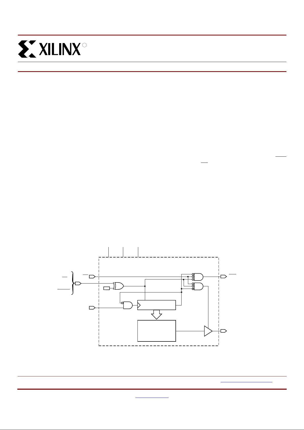
R
Figure 1: Simplified Block Diagram (does not show programming circuit)
EPROM
Cell
Matrix
Address Counter
CE
DATA
OE
Output
CLK
V
CC
V
PP
GND
DS027_01_021500
TC
OE
RESET/
OE/
RESET
or
CEO
Page 2
XC1700E and XC1700L Series Configuration PROMs
2 www.xilinx.com DS027 (v3.1) July 5, 2000
1-800-255-7778 Product Specification
R
Pin Description
DATA
Data output is in a high-impedance state when either CE or
OE
are inactive. During programming, the DATA pin is I/O.
Note that OE
can be programmed to be either active High or
active Low.
CLK
Each rising edge on the CLK input incr ements the inter nal
address counter, if both CE
and OE are active.
RESET/OE
When High, this input holds th e address counte r reset and
puts the DATA output in a high-impedance state. The polarity of this input pin is programmable as either RESET/OE
or
OE/RESET
. To avoid confusion, this document describes
the pin as RESET/OE
, although the opposite polarity is possible on all devices. When RESET is active, the address
counter is held at "0", and puts the DATA output in a
high-impedance state. The po larity of this input is programmable. The default is active High RESET, but the preferred
option is active Low RESET
, because it can be driven by the
FPGAs INIT
pin.
The polarity of this pin is controlled in the programmer interface. This input pin is easily inverted using the Xilinx
HW-130 Programmer. Third-party programmers have different methods to invert this pin.
CE
When High, this p in disables the inter nal address coun ter,
puts the DATA output in a high-impedance state, and forces
the device into low-I
CC
standby mode.
CEO
Chip Enable output, to be c onnect ed to th e C E input of the
next PROM in the daisy chain. This output is Low when the
CE
and OE inputs are both active AND the internal address
counter has been increm ented beyond its Termi nal Count
(TC) value. In other words: when the PROM has been read,
CEO
will follow CE as long as OE is active. When OE goes
inactive, CEO
stays High until the PROM is reset. Note that
OE
can be programmed to be either active High or active
Low .
V
PP
Programming voltage. No overshoot above the specified
max voltage is permitted on th is p in . For normal read oper ation, this pin must be connected to V
CC
. Failure to do so
may lead to unpredictable, temperature-dependent op eration and severe problems in circuit debugging. Do not leave
V
PP
floating!
VCC and GND
Positive supply and ground pins.
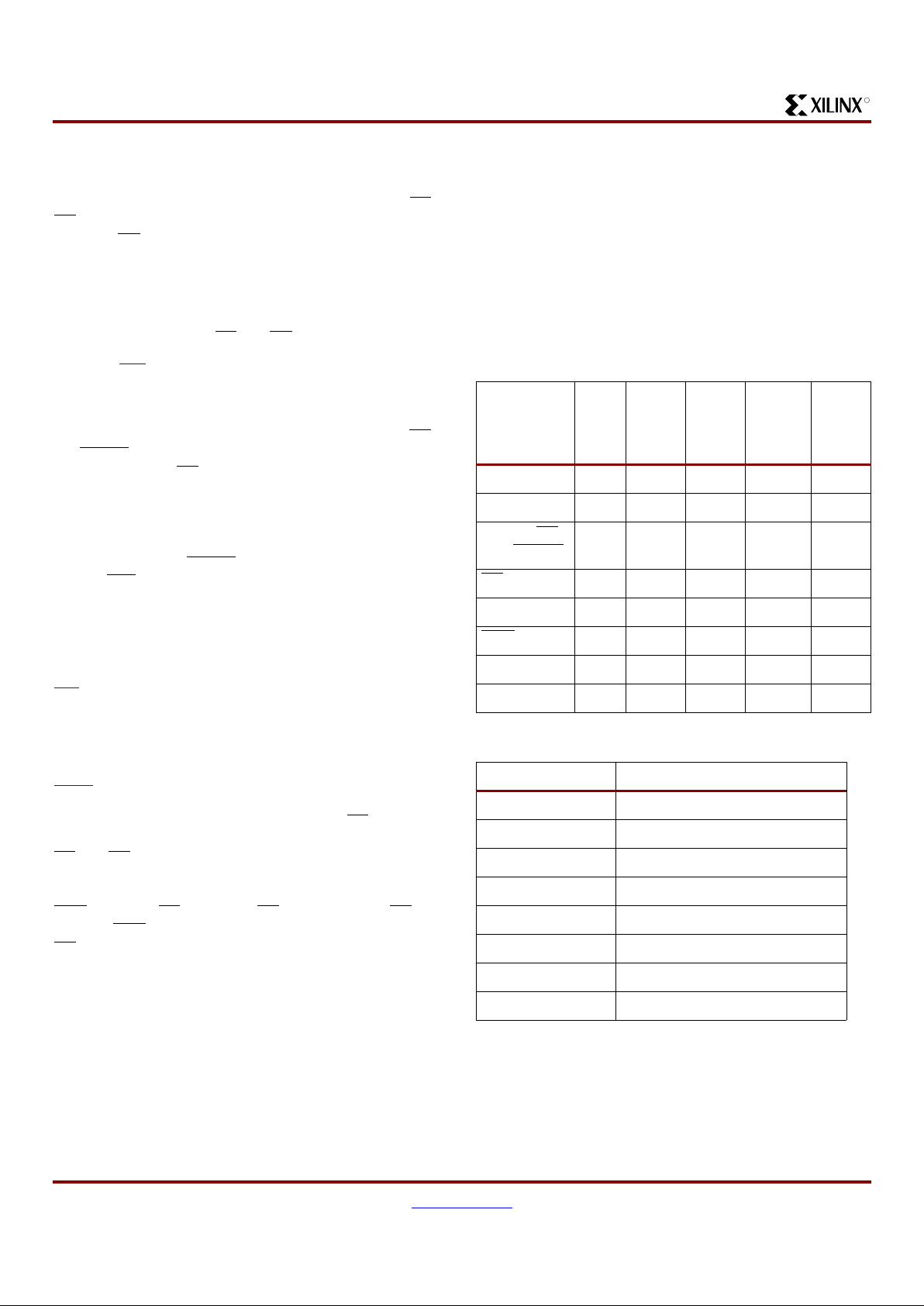
PROM Pinouts
Capacity
Pin Name
8-pin
PDIP
SOIC
VOIC
20-pin
SOIC
20-pin
PLCC
44-pin
VQFP
44-pin
PLCC
DATA 112402
CLK 2 3 4 43 5
RESET/OE
(OE/RESET)
38 6 1319
CE
4 10 8 15 21
GND 5 11 10 18, 41 24, 3
CEO
61314 2127
V
PP
71817 35 41
V
CC
82020 38 44
Devices Configuration Bits
XC1704L 4,194,304
XC1702L 2,097,152
XC1701/L 1,048,576
XC17512L 524,288
XC1736E 36,288
XC1765E/EL 65,536
XC17128E/EL 131,072
XC17256E/EL 262,144
Page 3
XC1700E and XC1700L Series Configuration PROMs
DS027 (v3.1) July 5, 2000 www.xilinx.com 3
Product Specification 1-800-255-7778
R
Xilinx FPGAs and Compatible PROMs
Device
Configuration
Bits PROM
XC4003E 53,984 XC17128E
(1)
XC4005E 95,008 XC17128E
XC4006E 119,840 XC17128E
XC4008E 147,552 XC17256E
XC4010E 178,144 XC17256E
XC4013E 247,968 XC17256E
XC4020E 329,312 XC1701
XC4025E 422,176 XC1701
XC4002XL 61,100 XC17128EL
(1)
XC4005XL 151,960 XC17256EL
XC4010XL 283,424 XC17512L
XC4013XL/XLA 393,632 XC17512L
XC4020XL/XLA 521,880 XC17512L
XC4028XL/XLA 668,184 XC1701L
XC4028EX 668,184 XC1701
XC4036EX/XL/XLA 832,528 XC1701L
XC4036EX 832,528 XC1701
XC4044XL/XLA 1,014,928 XC1701L
XC4052XL/XLA 1,215,368 XC1702L
XC4062XL/XLA 1,433,864 XC1702L
XC4085XL/XLA 1,924,992 XC1702L
XC40110XV 2,686,136 XC1704L
XC40150XV 3,373,448 XC1704L
XC40200XV 4,551,056 XC1704L +
XC17512L
XC40250XV 5,433,888 XC1704L+
XC1702L
XC5202 42,416 XC1765E
XC5204 70,704 XC17128E
XC5206 106,288 XC17128E
XC5210 165,488 XC17256E
XC5215 237,744 XC17256E
XCV50 559,232 XC1701L
XCV100 781,248 XC1701L
XCV150 1,041,128 XC1701L
XCV200 1,335,872 XC1702L
XCV300 1,751,840 XC1702L
XCV400 2,546,080 XC1704L
XCV600 3,608,000 XC1704L
XCV800 4,715,648 XC1704L +
XC1701L
XCV1000 6,127,776 XC1704L +
XC1702L
XCV50E 630,048 XC1701L
XCV100E 863,840 XC1701L
XCV200E 1,442,106 XC1702L
XCV300E 1,875,648 XC1702L
XCV400E 2,693,440 XC1704L
XCV405E 3,340,400 XC1704L
XCV600E 3,961,632 XC1704L
XCV812E 6,519,648 2 of XC170 4L
XCV1000E 6,587,520 2 of XC170 4L
XCV1600E 8,308,992 2 of XC170 4L
XCV2000E 10,159,648 3 of XC1704L
XCV2600E 12,922,336 4 of XC1704L
XCV3200E 16,283,712 4 of XC1704L
Notes:
1. The suggested PR OM is determined by compatibility w ith the
higher configuration frequency of the Xilinx FPGA CCLK.
Designers using the default slow configuration frequency
(CCLK) can use the XC1765E or XC1765EL for the noted
FPGA devices.
Device
Configuration
Bits PROM
Page 4

XC1700E and XC1700L Series Configuration PROMs
4 www.xilinx.com DS027 (v3.1) July 5, 2000
1-800-255-7778 Product Specification
R
Controlling PROMs
Connecting the FPGA device with the PROM.
• The DATA output(s) of th e of the PROM(s) drives the
D
IN
input of the lead FPGA device.
• The Master FPGA CCLK output drives the CLK input(s)
of the PROM(s).
• The CEO
output of a PROM drives the CE in put of the
next PROM in a daisy chain (if any).
• The RESET
/OE input of all PROMs is best driven by
the INIT
output of the lead FPGA device. This
connection assur es that th e PROM address counter is
reset before the start of any (re)configuration, even
when a reconfiguration is initiated by a V
CC
glitch.
Other methods—such as d riv in g RESE T
/OE from LDC
or system reset—assume the PROM internal
power-on-reset is always in step with the FPGA’s
internal power-on-reset. This may not be a safe
assumption.
• The PROM CE
input can be driven from either the LDC
or DONE pins. Using LDC avoids potential contention
on the D
IN
pin.
• The CE
input of the lead (or o nly) PROM is driven by
the DONE output of the lead FPGA device, provided
that DONE is not permanently grounded. Otherwise,
LDC
can be used to drive CE, but must then be
unconditionally High during user operation. CE
can
also be perm anently t ied Low, but this keeps the DATA
output active and causes an unnecessary supply
current of 10 mA maximum.
FPGA Master Serial Mode Summary
The I/O and logic functions of the Con figurable Logi c Block
(CLB) and their associated interconnections are established
by a configuration program. The program is loa ded either
automatically upon power up, or on command, depend ing
on the state of the three FPG A mo de p ins. In M aster Se rial
mode, the FPGA automatic ally lo ads th e con figuration program from an external memory. The Xilinx PROMs have
been designed for compatibility with the Master Serial
mode.
Upon power-up or reconfiguration, an FPGA enters the
Master Serial mode whenever all three of the FPGA
mode-select pins are Low (M0=0, M1=0, M2=0). Data is
read from the PROM sequentially on a single data line. Synchronization is provided by the rising edge of the temporary
signal CCLK, which is generated during configuration.
Master Serial Mod e provides a simple configuration interface. Only a serial data line and two control lines are
required to configure an FPGA. Data from the PROM is
read sequentially, accessed via the internal address and bit
counters which are inc remented on every valid ris ing edge
of CCLK.
If the user-programmable, dual-function D
IN
pin on the
FPGA is used only for configuration, it must still be held at a
defined level during normal operation. The Xilinx FPGA
families take care of this automatically with an on-chip
default pull-up resistor.
Programming the FPGA With Counters
Unchanged Upon Completion
When multiple FPGA-con figurations for a single FPGA are
stored in a PROM, the OE
pin should be tied Low. Upon
power-up, the internal address counte rs are re set and c onfiguration begins wit h the first program stored in memor y.
Since the OE
pin is held Low, the address coun ter s ar e le ft
unchanged after configuration is complete. Therefore, to
reprogram the FPGA with another program, the DONE line
is pulled Low and config uration begins at the last value of
the address counters.
This method fails if a user applies RESET
during the FPGA
configuration process. T he FPGA abor ts the configuration
and then restar ts a new configuration, as inten ded, but the
PROM does not reset its address counter, since it never
saw a High level on its OE
input. The new configuration,
therefore, reads the remaining data in the PROM and interprets it as preamble, length count etc. Si nce the FPGA is
the master, it issues the necessary number of CCLK pulses,
up to 16 million (2
24
) and DONE goes High. However, the
FPGA configuration will be completely wrong, with potential
contentions inside the FPGA and on its output pins. This
method must, therefore, never be used when there is any
chance of external reset during configuration.
Cascading Configuration PROMs
For multiple FPGAs configured as a daisy-chain, or for
future FPGAs requiring larger configuration memories, cascaded PROMs provide additional memo r y. After the last bit
from the first PROM is read, the next clock signal to the
PROM asser ts its CEO
output Low and disables its DATA
line. The second PROM recognizes the Low level on its CE
input and enables its DATA output. See Figure 2.
After configuration is complete, the a ddress coun ters of all
cascaded PROMs are reset if the FPGA RESET
pin goes
Low, assuming the PROM reset polarity option has been
inverted.
To re program the FPGA with another program, the DONE
line goes Low and configuration begi ns where the add ress
counters had stopped. In this case, avoid contention
between DATA and the configured I/O use of D
IN
.
Page 5

XC1700E and XC1700L Series Configuration PROMs
DS027 (v3.1) July 5, 2000 www.xilinx.com 5
Product Specification 1-800-255-7778
R
Figure 2: Master Serial Mode. The one-time-programmable PROM supports automatic loading of configuration programs.
Multiple devices can be cascaded to support additional FPGAs. An early DONE inhibits the PROM data output one CCLK
cycle before the FPGA I/Os become active.
D
IN
D
OUT
CCLK
INIT
DONE
PROM
DATA
CLK
CE CE
FPGA
(Low Resets the Address Pointer)
* For mode pin connections,
refer to the appropriate FPGA data sheet.
V
CC
V
CC
V
CC
OPTIONAL
Daisy-chained
FPGAs with
Different
configurations
OPTIONAL
Slave FPGAs
with Identical
Configurations
RESET RESET
DS027_02_060100
CCLK
(Output)
D
IN
D
OUT
(Output)
OE/RESET
MODES*
V
PP
Cascaded
Serial
Memory
DATA
CLK
CEO
OE/RESET
3.3V
4.7K
Page 6

XC1700E and XC1700L Series Configuration PROMs
6 www.xilinx.com DS027 (v3.1) July 5, 2000
1-800-255-7778 Product Specification
R
Standby Mode
The PROM enters a low-power standby mode whenever CE
is asser ted High. The output rem ains in a high impeda nce
state regardless of the state of the OE
input.
Programming
The devices can be programmed on programmers supplied
by Xilinx or qualified third-party vendors. The user must
ensure that the appropriate programming algorithm and the
latest version of the programmer software are used. The
wrong choice can permanently damage the device.
Table 1: Tr uth Table for XC1700 Control Inputs
Control Inputs
Internal Address
Outputs
RESET CE DATA CEO I
CC
Inactive Low If address < TC
(1)
: increment
If address > TC
(2)
: don’t change
Active
High-Z
High
Low
Active
Reduced
Active Low Held reset High-Z High Active
Inactive High Not changing High-Z High Standby
Active High Held reset High-Z High Standby
Notes:
1. The XC1700 RESET input has programmable polarity
2. TC = Terminal Count = highest address value. TC + 1 = address 0.
Page 7

XC1700E and XC1700L Series Configuration PROMs
DS027 (v3.1) July 5, 2000 www.xilinx.com 7
Product Specification 1-800-255-7778
R
XC1701, XC1736E, XC1765E, XC17128E and XC17256E
Absolute Maximum Ratings
Operating Conditions (5V Supply)
DC Characteristics Over Operating Condition
Symbol Description Conditions Units
V
CC
Supply voltage relative to GND –0.5 to +7.0 V
V
PP
Supply voltage relative to GND –0.5 to +12.5 V
V
IN
Input voltage relative to GND –0.5 to VCC +0.5 V
V
TS
Voltage applied to High-Z output –0.5 to VCC +0.5 V
T
STG
Storage temperature (ambient) –65 to +150
°
C
T
SOL
Maximum soldering temperature (10s @ 1/16 in.) +260
°
C
Notes:
1. Stresses beyond those listed under Absolute Maximum Ratings may cause permanent damage to the device.
These are stress r a ting s onl y, and functional opera tio n o f th e device at t hese or any other co ndi tio ns beyond thos e
listed under Operating Conditions is not implied. Exposure to Absolute Maximum Ratings conditions for extended
periods of time may affect device reliability.
Symbol Description Min Max Units
V
CC
(1)
Supply voltage relative to GND (TA = 0°C to +70°C) Commercial 4.750 5.25 V
Supply voltage relative to GND (T
A
= –40°C to +85°C) Industrial 4.50 5.50 V
Notes:
1. During normal read operation V
PP
MUST be connect to V
CC.
Symbol Description Min Max Units
V
IH
High-level input voltage 2 V
CC
V
V
IL
Low-level input voltage 0 0.8 V
V
OH
High-level output voltage (IOH = –4 mA) Commercial 3.86 - V
V
OL
Low-level output voltage (IOL = +4 mA) - 0.32 V
V
OH
High-level output voltage (IOH = –4 mA) Industrial 3.76 - V
V
OL
Low-level output voltage (IOL = +4 mA) - 0.37 V
I
CCA
Supply current, active mode (at maximum frequency) - 10 mA
I
CCS
Supply current, standby mode - 50
m
A
I
CCS
Supply current, standby mode (XC1701) - 100
m
A
I
L
Input or output leakage current –10 10
m
A
C
IN
Input capacitance (VIN = GND, f = 1.0 MHz) - 10 pF
C
OUT
Output capacitance (VIN = GND, f = 1.0 MHz) - 10 pF
Page 8

XC1700E and XC1700L Series Configuration PROMs
8 www.xilinx.com DS027 (v3.1) July 5, 2000
1-800-255-7778 Product Specification
R
XC1704L, XC1702L, XC1701L, XC17512L, XC1765EL, XC17128EL and XC17256EL
Absolute Maximum Ratings
Operating Conditions (3V Supply)
DC Characteristics Over Operating Condition
Symbol Description Conditions Units
V
CC
Supply voltage relative to GND –0.5 to +7.0 V
V
PP
Supply voltage relative to GND –0.5 to +12.5 V
V
IN
Input voltage relative to GND –0.5 to VCC +0.5 V
V
TS
Voltage applied to High-Z output –0.5 to VCC +0.5 V
T
STG
Storage temperature (ambient) –65 to +150
°
C
T
SOL
Maximum soldering temperature (10s @ 1/16 in.) +260
°
C
Notes:
1. Stresses beyond those listed under Absolute Maximum Ratings may cause permanent damage to the device.
These are stress r a ting s onl y, and functional opera tio n o f th e device at t hese or any other co ndi tio ns beyond thos e
listed under Operating Conditions is not implied. Exposure to Absolute Maximum Ratings conditions for extended
periods of time may affect device reliability.
Symbol Description Min Max Units
V
CC
(1)
Supply voltage relative to GND (TA = 0°C to +70°C) Commercial 3.0 3.6 V
Supply voltage relative to GND (T
A
= –40°C to +85°C) Industrial 3.0 3.6 V
Notes:
1. During normal read operation V
PP
MUST be connect to V
CC.
Symbol Description Min Max Units
V
IH
High-level input voltage 2 V
CC
V
V
IL
Low-level input voltage 0 0.8 V
V
OH
High-level output voltage (IOH = –3 mA) 2.4 - V
V
OL
Low-level output voltage (IOL = +3 mA) - 0.4 V
I
CCA
Supply current, active mode (at maximum frequency) (XC1700L) - 10 mA
I
CCA
Supply current, active mode (at maximum frequency)
(XC1765EL, XC17128EL, XC17256EL)
-5mA
I
CCS
Supply current, standby mode (XC1701L, XC17512L, XC17256L,
X1765EL, XC17128EL)
-50mA
I
CCS
Supply current, standby mode (XC1702L, XC1704L) - 350
m
A
I
L
Input or output leakage current –10 10
m
A
C
IN
Input capacitance (VIN = GND, f = 1.0 MHz) - 10 pF
C
OUT
Output capacitance (VIN = GND, f = 1.0 MHz) - 10 pF
Page 9

XC1700E and XC1700L Series Configuration PROMs
DS027 (v3.1) July 5, 2000 www.xilinx.com 9
Product Specification 1-800-255-7778
R
AC Characteristics Over Operating Condition
Symbol Description
XC1701,
XC17128E,
XC17256E
XC17128EL,
XC17256EL,
XC1704L,
XC1702L,
XC1701L,
XC17512L
XC1736E,
XC1765E XC1765EL
UnitsMin Max Min Max Min Max Min Max
T
OE
OE to data delay - 25 - 30 - 45 - 40 ns
T
CE
CE to data delay - 45 - 45 - 60 - 60 ns
T
CAC
CLK to data delay - 45 - 45 - 80 - 200 ns
T
DF
CE or OE to data float delay
(2,3)
- 50 - 50 - 50 - 50 ns
T
OH
Data hold from CE, OE, or CLK
(3)
0-0 -0-0-ns
T
CYC
Clock periods 67 - 67 - 100 - 400 - ns
T
LC
CLK Low time
(3)
20 - 25 - 50 - 100 - ns
T
HC
CLK High time
(3)
20 - 25 - 50 - 100 - ns
T
SCE
CE setup time to CLK
(to guarantee proper counting)
20 - 25 - 25 - 40 - ns
T
HCE
CE hold time to CLK
(to guarantee proper counting)
0-0 -0-0-ns
T
HOE
OE hold time
(guarantees counters are reset)
20 - 25 - 100 - 100 - ns
Notes:
1. AC test load = 50 pF
2. Float delays are measured with 5 pF AC loads. Transition is measured at ±200 mV from steady state active levels.
3. Guaranteed by design, not tested.
4. All AC parameters are measured with VIL = 0.0V and VIH = 3.0V.
RESET/OE
CE
CLK
DATA
T
CE
T
OE
T
LC
T
SCE
T
SCE
T
HCE
T
HOE
T
CAC
T
OH
T
DF
T
OH
T
HC
DS027_03_021500
T
CYC
Page 10

XC1700E and XC1700L Series Configuration PROMs
10 www.xilinx.com DS027 (v3.1) July 5, 2000
1-800-255-7778 Product Specification
R
AC Characteristics Over Operating Condition When Cascading
Symbol Description Min Max Units
T
CDF
CLK to data float delay
(2,3)
-50 ns
T
OCK
CLK to CEO delay
(3)
-30 ns
T
OCE
CE to CEO delay
(3)
-35 ns
T
OOE
RESET/OE to CEO delay
(3)
-30 ns
Notes:
1. AC test load = 50 pF
2. Float delays are measured with 5 pF AC loads. Transition is measured at ±200 mV from steady
state active levels.
3. Guaranteed by design, not tested.
4. All AC parameters are measured with V
IL
= 0.0V and VIH = 3.0V.
RESET/OE
CLK
DATA
CE
T
OOE
CEO
First Bit Last Bit
T
OCE
T
OCK
T
CDF
DS027_04_021500
T
OCE
Page 11

XC1700E and XC1700L Series Configuration PROMs
DS027 (v3.1) July 5, 2000 www.xilinx.com 11
Product Specification 1-800-255-7778
R
Ordering Information
Valid Ordering Combinations
XC1736EPD8C XC1765EPD8C XC17128EPD8C XC17256EPD8C XC1701PD8C XC1702LVQ44C
XC1736ESO8C XC1765ESO8C XC17128EVO8C XC17256EVO8C XC1701PC20C XC1702LPC44C
XC1736EVO8C XC1765EVO8C XC17128EPC20C XC17256EPC20C XC1701SO20C XC1704LVQ44C
XC1736EPC20C XC1765EPC20C XC17128EPD8I XC17256EPD8I XC1701PD8I XC1704LPC44C
XC1736EPD8I XC1765EPD8I XC17128EVO8I XC17256EVO8I XC1701PC20I XC1702LVQ44I
XC1736ESO8I XC1765ESO8I XC17128EPC20I XC17256EPC20I XC1701SO20I XC1702LPC44I
XC1736EVO8I XC1765EVO8I XC1704LVQ44I
XC1736EPC20I XC1765EPC20I XC1704LPC44I
XC1765ELPD8C XC17128ELPD8C XC17256ELPD8C XC1701LPD8C XC17512LPD8C
XC1765ELSO8C XC17128ELVO8C XC17256ELVO8C XC1701LPC20C XC17512LPC20C
XC1765ELVO8C XC17128ELPC20C XC17256ELPC20C XC1701LSO20C XC17512LSO20C
XC1765ELPC20C XC17128ELPD8I XC17256ELPD8I XC1701LPD8I XC17512LPD8I
XC1765ELPD8I XC17128ELVO8I XC17256ELVO8I XC1701LPC20I XC17512LPC20I
XC1765ELSO8I XC17128ELPC20I XC17256ELPC20I XC1701LSO20I XC17512LSO20I
XC1765ELVO8I
XC1765ELPC20I
XC1701L PC20 C
Operating Range/Processing
C = Commercial (T
A =
0° to +70°C)
I = Industrial (T
A
= –40° to +85°C)
Package Type
PD8 = 8-pin Plastic DIP
SO8 = 8-pin Plastic Small-Outline Package
VO8 = 8-pin Plastic Small-Outline Thin Package
SO20 = 20-pin Plastic Small-Outline Package
PC20 = 20-pin Plastic Leaded Chip Carrier
VQ44 = 44-pin Plastic Quad Flat Package
PC44 = 44-pin Plastic Chip Carrier
Device Number
XC1736E
XC1765E
XC1765EL
XC17128E
XC17128EL
XC17256E
XC17256EL
XC17512L
XC1701
XC1701L
XC1704L
XC1702L
Page 12

XC1700E and XC1700L Series Configuration PROMs
12 www.xilinx.com DS027 (v3.1) July 5, 2000
1-800-255-7778 Product Specification
R
Marking Information
Due to the small s ize of the c ommer cial s eri al P ROM packages, the com plete order ing part number c annot be mar ked on
the package. The XC prefix is deleted and the package code is simplified. Device marking is as follows:
Revision History
The following table shows the revision history for this document.
Notes:
1. When marking the device number on the EL parts, an X is used in place of an EL.
2. For XC1700E/EL only.
3. For XC1700L only.
1701L J C
Operating Range/Processing
C = Commercial (T
A =
0° to +70°C)
I = Industrial (T
A
= –40° to +85°C)
Package Type
P = 8-pin Plastic DIP
S
(2)
= 8-pin Plastic Small-Outline Package
V = 8-pin Plastic Small-Outline Thin Package
S
(3)
= 20-pin Plastic Small-Outline Package
J = 20-pin Plastic Leaded Chip Carrier
VQ44 = 44-pin Plastic Quad Flat Package
PC44 = 44-pin Plastic Chip Carrier
Device Number
1736E
1765E
1765X
(1)
17128E
17128X
(1)
17256E
17256X
(1)
1704L
1702L
1701
1701L
17512L
Date Version Revision
7/14/98 1.1 Major revisions to include the XC1704L, XC1702L, and the XQ1701L devices, packages and
operating conditions. Also revised the timing specifications on page 9.
9/8/98 2.0 Revised the marking information for the VQ44. Updated "DC Characteristics Over Operating
Condition" on page 7 and page 8. Added references to the XC4000XLA and XC4000XV
families in "Xilinx FPGAs and Compatible PROMs" on page 3 and Figure 2 on page 5.
12/18/98 2.1 Added Virtex FPGAs to "Xilinx FPGAs and Compatible PROMs" on page 3. Added the PC44
package for the XC1702L and XC1704L products.
1/27/99 2.2 Changed Military I
CCS
.
7/8/99 2.3 Changed I
CCS
standby on XC1702/XC1704 from 50 mA to 300 mA.
3/30/00 3.0 Combined data sheets XC1700E and XC1700L. Added DS027, removed Military Specs.
Added Virtex-E and EM references.
07/05/00 3.1 Added 4.7K resistor to Figure 2, updated format.
 Loading...