XICOR X9015USI-2.7, X9015USI, X9015US Datasheet

Low Noise, Low Power
X9015
Digitally-Controlled Potentiometer
FEATURES
• 32 T aps
• Three-wire Up/Down Serial Interface
•V
= 2.7V & 5V
CC
• Operating I
= 50µA Max.
CC
• Standby current = 1µA Max.
•R
TOTAL
= 50K Ω
• Packages, SOIC-8
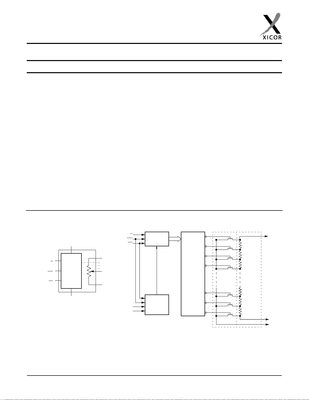
FUNCTIONAL DIAGRAMS
DESCRIPTION
The Xicor X9015 is a 32 tap potentiometer that is volatile.
The device consists of a string of 31 resistors that can be
programmed to connect the R
/V
wiper output with
W
W
any of the nodes between the connecting resistors. The
connection point of the wiper is determined by
information communicated to the device on the 3-wire
port. The 3-wire port changes the tap position by a f alling
edge on the increment pin. Direction the wiper moves is
determined by the state of the Up/Down pin. The wiper
position at power up is tap #15.
The X9015 can be used in a wide variety of applications
that require a digitally controlled variable resistor to set
analog values.
UP/DOWN
(U/D
)
INCREMENT
(INC
)
DEVICE SELECT
9900-2009.3 9/20/99 PS
(CS
)
V
(Supply Voltage)
CC
CONTROL
V
(Ground)
SS
GENERAL
R
H/VH
RW/V
RL/V
U/D
INC
CS
W
L
V
CC
V
SS
5-BIT
UP/DOWN
COUNTER
CONTROL
CIRCUITRY
1
ONE
OF
THIRTY TWO
DECODER
DETAILED
31
30
29
28
TRANSFER
GATES
2
1
0
Characteristics subject to change without notice
RESISTOR
ARRAY
RH/V
RL/V
RW/V
H
L
W

X9015
V
CC
CS
INC
U/D
RH/V
H
V
SS
1
2
3
4
8
7
6
5
X9015
SOIC
R
L/VL
RW/V
W
PIN DESCRIPTIONS
R
/V
and R
H
H
The high (R
/V
L
L
/V
) and low (R
H
H
/V
) terminals of the
L
L
X9015 are equivalent to the fixed terminals of a
mechanical potentiometer. The minimum voltage is V
and the maximum is V
R
/V
references the relative position of the terminal in
H
H
. The terminology of R
CC
SS
/V
and
L
L
relation to wiper movement direction selected by the
U/D input and not the voltage potential on the terminal.
R
/V
W
W
R
/V
is the wiper terminal and is equivalent to the
W
w
movable terminal of a mechanical potentiometer. The
position of the wiper within the array is determined by the
control inputs. The wiper terminal series resistance is
typically 200 Ω at V
position is at tap #15 (V
= 5V. At power up the wiper
CC
/R
= tap #0).
L
L
Up/Down (U/D)
The U/D input controls the direction of the wiper
movement and whether the tap postion is incremented or
decremented.
Increment (INC)
The INC input is negative-edge triggered. Toggling INC
will move the wiper and either increment or decrement
the counter in the direction indicated by the logic level on
the U/D input.
Chip Select (CS)
The device is selected when the CS input is LOW. When
CS is returned HIGH while the INC input is LOW the
X9015 will be placed in the low power standby mode until
the device is selected once again.
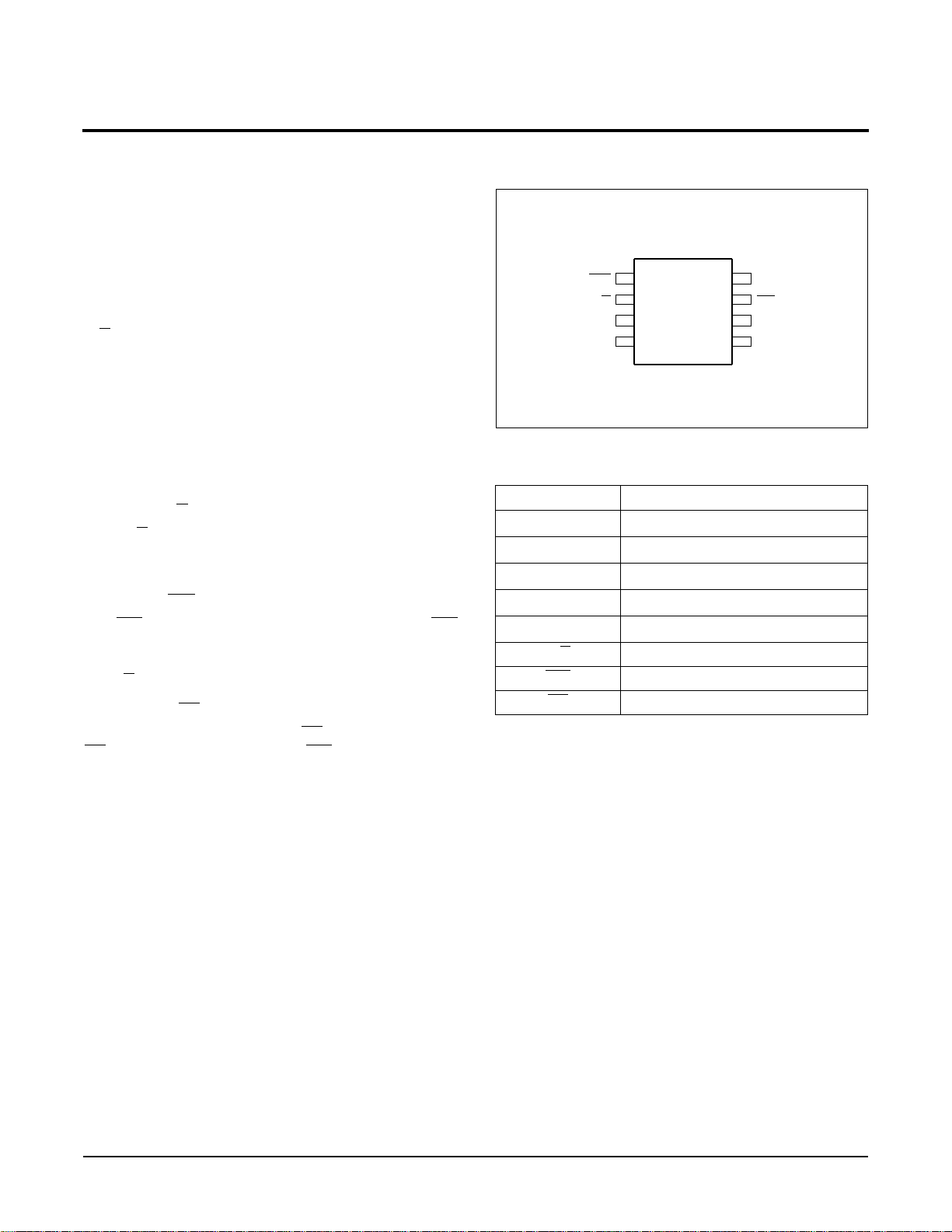
PIN CONFIGURATION
PIN NAMES
Symbol Description
R
R
W
R
V
V
U/D
INC
H
L
SS
CC
CS
/V
/V
/V
H
W
L
High Terminal
Wiper Terminal
Low Terminal
Ground
Supply Voltage
Up/Down Control Input
Increment Control Input
Chip Select Control Input
2

X9015
PRINCIPLES OF OPERATION
There are two sections of the X9015: the input control,
counter and decode section; and the resistor array. The
input control section operates just like an up/down
counter. The output of this counter is decoded to turn on
a single electronic switch connecting a point on the resistor array to the wiper output. The resistor array is comprised of 31 individual resistors connected in series.
The wiper, when at either fixed terminal, acts like its
mechanical equivalent and does not move beyond the
last position. That is, the counter does not wrap around
when clocked to either e xtreme.
The electronic switches on the device oper ate in a “mak e
before break” mode when the wiper changes tap
positions. If the wiper is mo v ed several positions, multiple
taps are connected to the wiper for t
change). The R
value for the device can
TOT AL
(INC to V
IW
W
temporarily be reduced by a significant amount if the
wiper is moved se veral positions .
When the device is powered-down, the wiper position is
lost. When po wer is restored, the wiper is set to tap #15.
INSTRUCTIONS AND PROGRAMMING
The INC, U/D and CS inputs control the mov ement of the
wiper along the resistor array. With CS set LOW the
device is selected and enabled to respond to the U/D and
INC inputs. HIGH to LOW transitions on INC will
increment or decrement (depending on the state of the
U/D input) a five bit counter. The output of this counter is
decoded to select one of thirty two wiper positions along
the resistive array.
The system may select the X9015, move the wiper and
deselect the device. The new wiper position will be
maintained until changed by the system or until a powerup/down cycle.
The state of U/D may be changed while CS remains
LOW. This allows the host system to enable the device
and then move the wiper up and down until the proper
trim is attained.
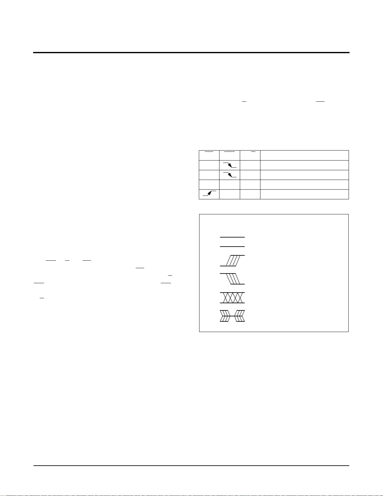
MODE SELECTION
CS INC U/D Mode
L H Wiper Up
L L Wiper Down
H X X Standby Current
L X Return to standby
SYMBOL TABLE
WAVEFORM INPUTS OUTPUTS
Must be
steady
May change
from Low to
High
May change
from High to
Low
Don’t Care:
Changes
Allowed
N/A Center Line
Will be
steady
Will change
from Low to
High
Will change
from High to
Low
Changing:
State Not
Known
is High
Impedance
3

X9015
∆
≤
Ω
Ω
ABSOLUTE MAXIMUM RATINGS*
Temperature under Bias.........................–65 ° C to +135 ° C
Storage Temperature..............................–65°C to +150°C
V oltage on CS, INC , U/D , V
with Respect to V
V = |V
–V
| .................................................................5V
H
L
, V
and V
H
L
..................................–1V to +7V
SS
CC
Lead Temperature (Soldering 10 seconds)............. 300°C
*COMMENT
Stresses above those listed under “Absolute Maximum
Ratings” may cause permanent damage to the device.
This is a stress rating only and the functional operation of
the device at these or any other conditions above those
listed in the operational sections of this specification is
not implied. Exposure to absolute maxim um rating conditions for extended periods ma y affect de vice reliability.
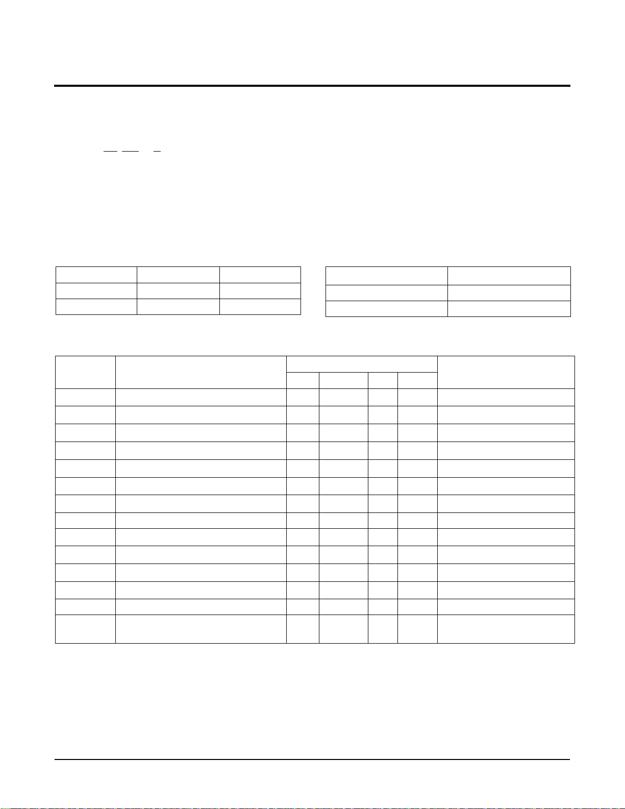
RECOMMENDED OPERATING CONDITIONS
Temperature Min. Max.
Commercial 0°C +70°C
Industrial –40°C +85°C
Supply Voltage (V
CC
)
X9015 5V ±10%
X9015-2.7 2.7V to 5.5V
Limits
POTENTIOMETER CHARACTERISTICS (Over recommended operating conditions unless otherwise stated.)
Limits
Symbol Parameter
R
TOTAL
V
VH
V
VL
End to End Resistance Variation –20 +20 %
V
Terminal Voltage
H
V
Terminal Voltage
L
Power Rating 10 mW
R
W
R
W
I
W
Wiper Resistance 200 400
Wiper Resistance 400 1000
Wiper Current ±1 mA
0
0
V
CC
V
CC
V
V
Test Conditions/NotesMin. Typ. Max. Units
R
TOTAL
I
= 1mA, V
W
I
= 1mA, V
W
50K Ω
CC
CC
= 5V
= 2.7V
Noise -120 dBV Ref: 1kHz
Resolution
Absolute Linearity
Relative Linearity
R
Temperature Coefficient
TOTAL
(2)
(1)
-1 +1
-0.2 +0.2
3%
(3)
(3)
V
w(n)(actual)
V
w(n+1)
MI
MI
±300 ppm/°C
– [V
– V
w(n)(expected)
w(n)+MI
]
Ratiometric Temperature Coefficient ±20 ppm/°C
C
H/CL/CW
Potentiometer Capacitances
10/10/25
pF See circuit #3
Notes: (1) Absolute Linearity is utilized to determine actual wiper voltage versus expected voltage
= (V
(actual) – V
w(n)
(2) Relative Linearity is a measure of the error in step size between taps = V
(3) 1 Ml = Minimum Increment = R
(4) T ypical v alues are f or T
(5) This parameter is periodically sampled and not 100% tested.
(expected)) = ±1 Ml Maximum.
w(n)
/31.
TOT
= 25°C and nominal supply voltage.
A
– [V
W(n+1)
4
w(n)
+ Ml] = ±0.2 Ml.
 Loading...