X88C64 SLIC® E
2
1
© Xicor, Inc. 1993, 1995, 1996 Patents Pending Characteristics subject to change without notice
6540-1.5 7/9/96 T0/C1/D0 NS
E2 Micro-Peripheral
64K X88C64 SLIC
®
E
2
8192 x 8 Bit
80C51 Microcontroller Family Compatible
SLIC® E2 and CONCURRENT READ WRITE™ are trademarks of Xicor, Inc.
DESCRIPTION
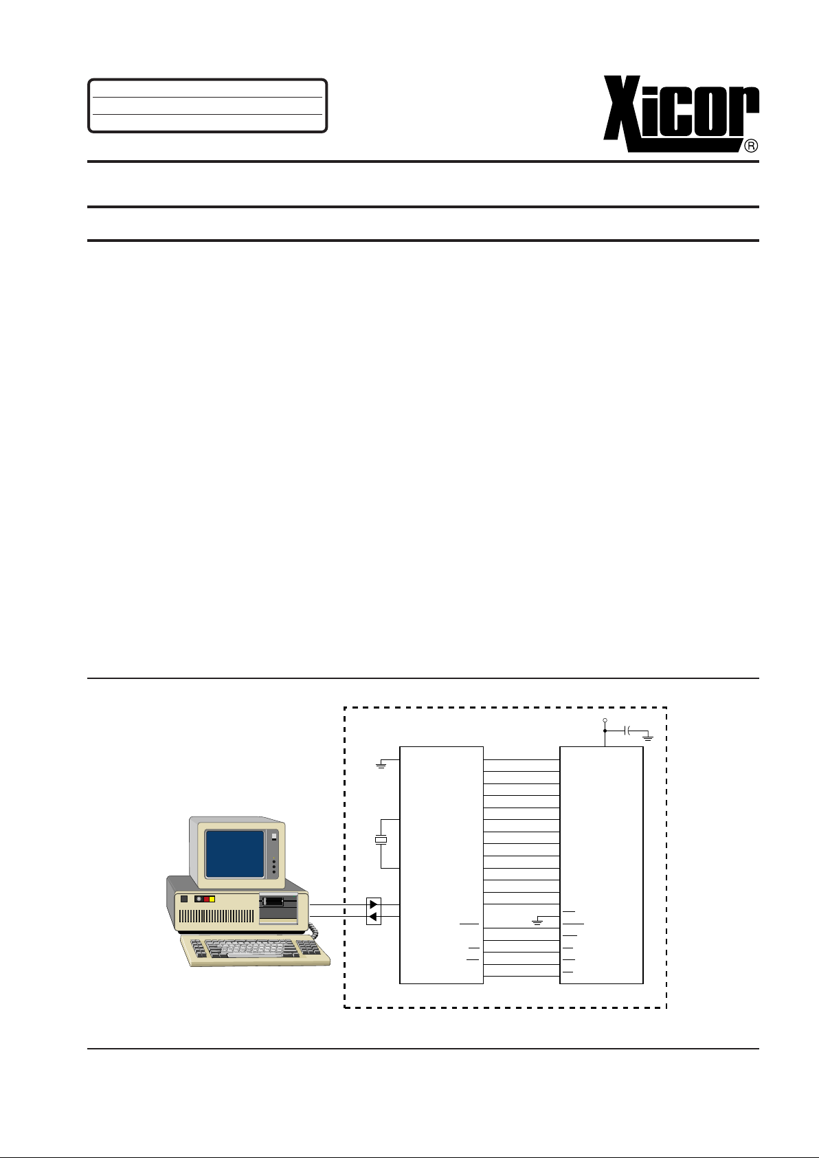
The X88C64 SLIC E2 is a highly integrated E2 Microcontroller peripheral which combines the functionality of the X88C64 component with pre-loaded software routines allowing any embedded system using
it to upgrade and download software via the serial
port. This self-loading integrated code eliminates the
need to initially program the firmware into a memory
device at the time of initial manufacture. The SLIC
routines also greatly facilitate the loading of subsequent versions of the firmware into the system.
The SLIC routines consist of approximately 500 bytes
of instructions for the 8051 which will initialize the
microcontroller and its on-board UART and download
the user’s software through the UART. The baud rate
for the transfer is 9600 based on a crystal frequency
of 11MHz. Data transfer is accomplished using a
proprietary format called XCOM. Xicor also has developed a program for IBM PCs and compatibles
called XSLIC, which will translate an Intel HEX format
file into XCOM format and upload the program to an
X88C64 SLIC E2.
The X88C64 device itself is an 8K x 8 E2PROM
fabricated with advanced CMOS Textured Poly Float-
FEATURES
SLIC (SELF LOADING INTEGRATED CODE)
FIRMWARE
• Automatically Downloads User’s Software into
8051 Based Systems
• Features Load, Verify, and Block Protection
Capabilities
• Transfers Baud Rate 9600 at 11MHz
• CONCURRENT READ WRITE
™
—Dual Plane Architecture
—Isolates Read/Write Functions
Between Planes
—Allows Continuous Execution of Code
From One Plane While Writing in
the Other Plane
• Multiplexed Address/Data Bus
—Direct Interface to Popular 8051 Family
• Block Protect Register
—Individually Set Write Lock Out in 1K Blocks
• Toggle Bit Polling
—Early End of Write Detection
• Page Mode Write
—Allows up to 32 Bytes to be Written in
One Write Cycle
APPLICATION NOTES AND DEVELOPMENT SYSTEM
AVAILABLE
AN62–64 • AN66 • AN68 • XK88
TYPICAL APPLICATION
7
8
9
10
11
13
14
15
21
20
17
19
2
5
6
22
18
23
16
A/D0
A/D1
A/D2
A/D3
A/D4
A/D5
A/D6
A/D7
A8
A9
A10
A11
A12
WC
PSEN
ALE
RD
WR
CE
V
CC
24
Target System
X88C64 SLIC
®
E
2
39
38
37
36
35
34
33
32
21
22
23
24
25
29
30
17
16
P0.0
P0.1
P0.2
P0.3
P0.4
P0.5
P0.6
P0.7
P2.0
P2.1
P2.2
P2.3
P2.4
PSEN
ALE
RD
WR
P2.7
80C51 µC Family
EA/VP
X1
X2
P3.0
P3.1
31
19
18
RS232
DRIVERS
IBM PC
OR
COMPATIBLE
6540 ILL F01.1

X88C64 SLIC® E
2
2
ing Gate Technology. The X88C64 features a Multiplexed Address and Data bus allowing direct interface to a variety of popular single-chip microcontrollers
operating in expanded multiplexed mode without the
need for additional interface circuitry.
The X88C64 is internally configured as two independent 4K x 8 memory arrays. This feature provides the
ability to perform nonvolatile memory updates in one
array and continue operation out of code stored in the
other array; effectively eliminating the need for an
auxiliary memory device for code storage.
To write to the X88C64 SLIC E2, a three-byte command sequence must precede the byte(s) being written. This sequence called Software Data Protection
prevents the loss of data or program information due
to inadvertant write cycles during power-up or powerdown. The X88C64 SLIC E2 also provides a second
generation software data protection scheme called
Block Protect.
Block Protect can provide write lockout of the entire
device or selected 1K blocks. There are eight 1K x 8
blocks that can be write protected individually in any
combination required by the user. Block Protect, in
additional to Write Control input, allows the different
segments of the memory to have varying degrees of
alterability in normal system operation.
For further information on the X88C64 hardware
interface, consult the X88C64 Data Sheet.
PIN NAMES
Symbol Description
ALE Address Latch Enable
A/D0–A/D
7
Address Inputs/Data I/O
A8–A
12
Address Inputs
RD Read Input
WR Write Input
PSEN Program Store Enable Input
CE Chip Enable
WC Write Control
V
SS
Ground
V
CC
Supply Voltage
6540 PGM T01
PIN CONFIGURATION
DIP/SOIC
6540 FHD F02
NC
A12
NC
NC
WC
PSEN
A/D0
A/D1
A/D2
A/D3
A/D4
V
SS
1
2
3
4
5
6
7
8
9
10
11
12
24
23
22
21
20
19
18
17
16
15
14
13
V
CC
WR
ALE
A8
A9
A11
RD
A10
CE
A/D7
A/D6
A/D5
X88C64
 Loading...