XICOR X88C64SMB, X88C64SM, X88C64SI, X88C64S, X88C64PMB Datasheet
...
APPLICATION NOTE
AVAILABLE
AN63
X88C64
8051 Microcontroller Family Compatible
SLIC
64K X88C64 8192 x 8 Bit
E2 Micro-Peripheral
FEATURES
• CONCURRENT READ WRITE
™
—Dual Plane Architecture
—Isolates Read/Write Functions
Between Planes
—Allows Continuous Execution of Code
From One Plane While Writing in
the Other Plane
• Multiplexed Address/Data Bus
—Direct Interface to Popular 8051 Family
• High Performance CMOS
—Fast Access Time, 120ns
—Low Power
—60mA Active Maximum
—500µA Standby Maximum
• Software Data Protection
• Block Protect Register
—Individually Set Write Lock Out in 1K Blocks
• Toggle Bit Polling
—Early End of Write Detection
• Page Mode Write
—Allows up to 32 Bytes to be Written in
One Write Cycle
• High Reliability
—Endurance: 100,000 Write Cycle
—Data Retention: 100 Years
DESCRIPTION
The X88C64 is an 8K x 8 E2PROM fabricated with
advanced CMOS Textured Poly Floating Gate Technology. The X88C64 features a Multiplexed Address
and Data bus allowing a direct interface to a variety of
popular single-chip microcontrollers operating in expanded multiplexed mode without the need for additional interface circuitry.
The X88C64 is internally configured as two independent 4K x 8 memory arrays. This feature provides the
ability to perform nonvolatile memory updates in one
array and continue operation out of code stored in the
other array; effectively eliminating the need for an
auxiliary memory device for code storage.
To write to the X88C64, a three-byte command
sequence must precede the byte(s) being written. The
X88C64 also provides a second generation software
data protection scheme called Block Protect. Block
Protect can provide write lockout of the entire device
or selected 1K blocks. There are eight 1K x 8 blocks
that can be write protected individually in any combination required by the user. Block Protect, in addition
to Write Control input, allows the different segments
of the memory to have varying degrees of alterability
in normal system operation.
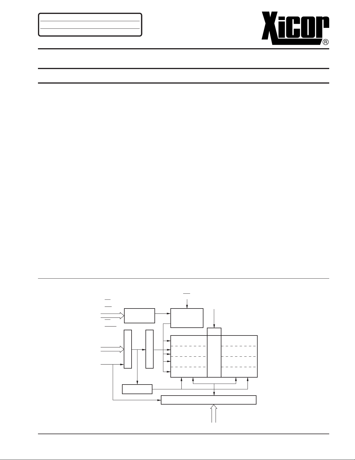
FUNCTIONAL DIAGRAM
WC
CE
WR
RD
PSEN
A8–A
ALE
CONCURRENT READ WRITE™ is a trademark of Xicor, Inc.
© Xicor, Inc. 1994, 1995, 1996 Patents Pending Characteristics subject to change without notice
3867-1.5 7/9/96 T0/C2/D0 NS
11
CONTROL
LOGIC
L
A
T
C
H
E
S
Y DECODE
SOFTWARE
DATA
PROTECT
X
D
E
C
O
D
E
1K BYTES
1K BYTES
1K BYTES
1K BYTES
I/O & ADDRESS LATCHES AND BUFFERS
1
A12
A
12
A
12
M
U
X
1K BYTES
1K BYTES
1K BYTES
1K BYTES
A/D0–A/D
7
3867 FHD F02

X88C64
PIN DESCRIPTIONS
Address/Data (A/D0–A/D7)
Multiplexed low-order addresses and data. The Addresses flow into the device while ALE is HIGH. After
ALE transitions from a HIGH to LOW the addresses
are latched. Once the addresses are latched these
pins input data or output data depending on RD, WR,
PSEN, and CE.
Addresses (A8–A12)
High order addresses flow into the device when ALE
is HIGH and are latched when ALE goes LOW.
Chip Enable (CE)
The Chip Enable input must be LOW to enable all
read/write operations. When CE is HIGH and ALE is
LOW, the X88C64 is placed in the low power standby
mode.
Program Store Enable (PSEN)
When the X88C64 is to be used in a 8051 based
system, PSEN is tied directly to the microcontroller’s
PSEN output.
When WC is LOW (tied to VSS) the X88C64 will be
enabled to perform write operations. When WC is
HIGH normal read operations may be performed, but
all attempts to write to the device will be disabled.
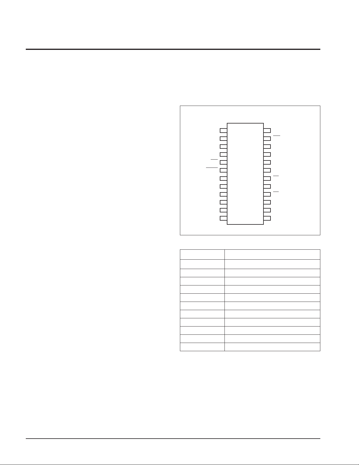
PIN CONFIGURATION
DIP/SOIC
NC
A12
NC
NC
WC
PSEN
A/D0
A/D1
A/D2
A/D3
A/D4
V
SS
1
2
3
4
5
6
7
8
9
10
11
12
X88C64
24
23
22
21
20
19
18
17
16
15
14
13
V
CC
WR
ALE
A8
A9
A11
RD
A10
CE
A/D7
A/D6
A/D5
3867 FHD F01
Read (RD)
When the X88C64 is to be used in a 8051 based
system, RD is tied directly to the microcontroller’s RD
output.
Write (WR)
When the X88C64 is to be used in a 8051 based
system, WR is tied directly to the microcontroller’s
WR output.
Address Latch Enable (ALE)
Addresses flow through the latches to address decoders when ALE is HIGH and are latched when ALE
transitions from a HIGH to LOW.
Write Control (WC)
The Write Control allows external circuitry to abort a
page load cycle once it has been initiated. This input
is useful in applications in which a power failure or
processor RESET could interrupt a page load cycle.
In this case, the microcontroller might drive all signals
HIGH, causing bad data to be latched into the
E2PROM. If the Write Control input is driven HIGH
(before t
Max) after Write (WR) goes HIGH, the
BLC
write cycle will be aborted.
PIN NAMES
Symbol Description
ALE Address Latch Enable
A/D0–A/D
A8–A
12
7
Address Inputs/Data I/O
Address Inputs
RD Read Input
WR Write Input
PSEN Program Store Enable Input
CE Chip Enable
WC Write Control
V
SS
V
CC
Ground
Supply Voltage
NC No Connect
3867 PGM T01.1
2

X88C64
PRINCIPLES OF OPERATION
The X88C64 is a highly integrated peripheral device for
a wide variety of single-chip microcontrollers. The
X88C64 provides 8K bytes of E2PROM which can be
used either for Program Storage, Data Storage, or a
combination of both in systems based upon Harvard
(80XX) architectures. The X88C64 incorporates the
interface circuitry normally needed to decode the control
signals and demultiplex the Address/Data bus to provide a “Seamless” interface.
The interface inputs on the X88C64 are configured such
that it is possible to directly connect them to the proper
interface signals of the appropriate single-chip
microcontroller. In the Harvard type system, the reading
of data from the chip is controlled either by the PSEN or
the RD signal, which essentially maps the X88C64 into
both the Program and the Data Memory address map.
The X88C64 is internally organized as two independent
planes of 4K bytes of memory with the A12 input selecting which of the two planes of memory are to be
accessed. While the processor is executing code out of
one plane, write operations can take place in the other
plane, allowing the processor to continue execution of
code out of the X88C64 during a byte or page write to the
device.
The X88C64 also features an advanced implementation
of the Software Data Protection scheme, called Block
Protect, which allows the device to be broken into 8
independent sections of 1K bytes. Each of these sections can be independently enabled for write operations;
thereby allowing certain sections of the device to be
secured so that updates can only occur in a controlled
environment (e.g. in an automotive application, only at
an authorized service center). The desired set-up configuration is stored in a nonvolatile register, ensuring the
configuration data will be maintained after the device is
powered down.
The X88C64 also features a Write Control input (WC),
which serves as an external control over the completion
of a previously initiated page load cycle.
The X88C64 also features the industry standard
E2PROM characteristics such as byte or page mode
write and Toggle Bit Polling.
DEVICE OPERATION
MODES
Mixed Program/Data Memory
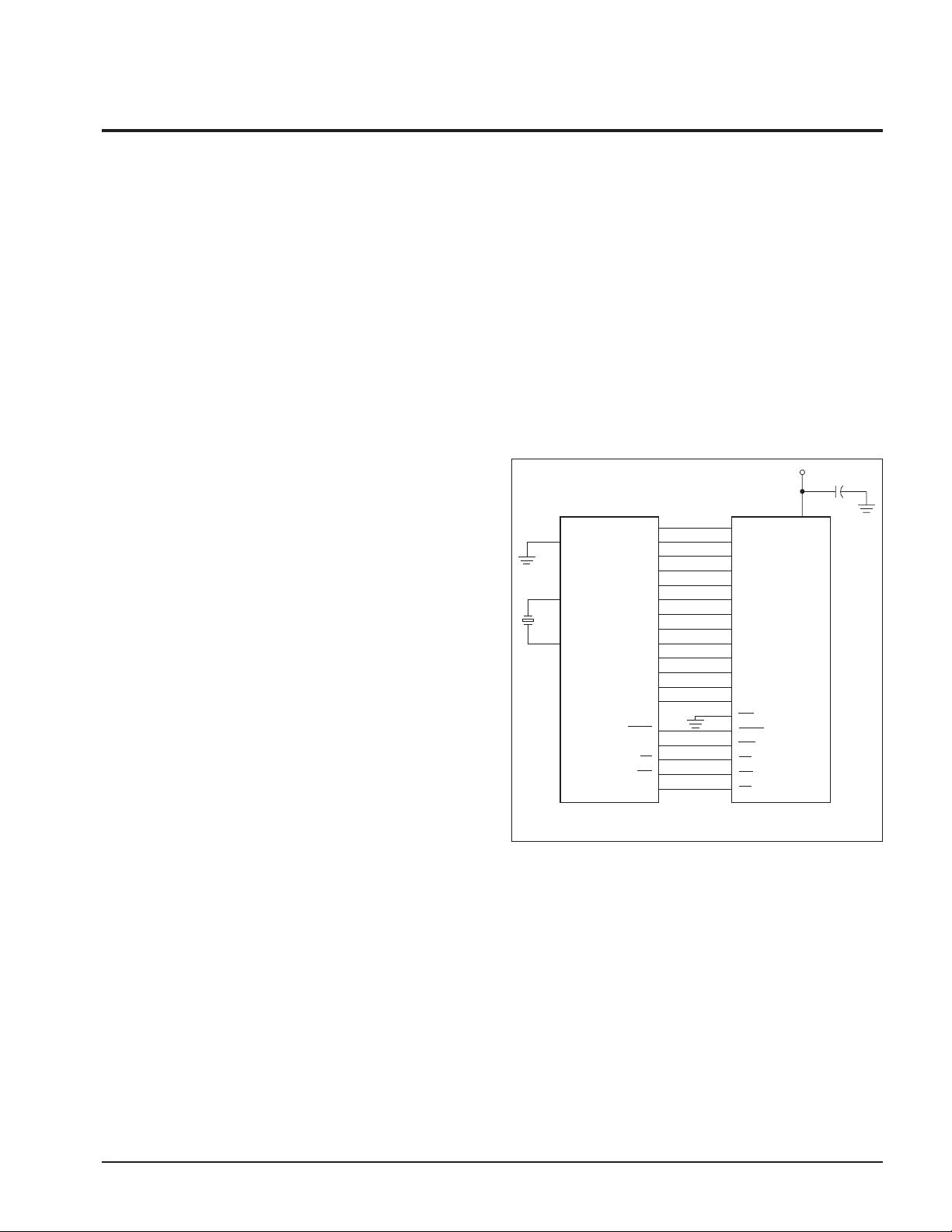
By properly assigning the address spaces, a single
X88C64 can be used as both the Program and Data
Memory. This would be accomplished by connecting all
of the 8051 control outputs to the corresponding inputs
of the X88C64.
In this configuration, one plane of memory could be
dedicated to Program Storage and the other plane
dedicated to Data Storage. The Data Storage can be
fully protected by enabling block protect write lockout.
TYPICAL APPLICATION
X88C6480C31
24
V
CC
3867 FHD F03
39
31
EA/VP
19
X1
18
X2
P0.0
P0.1
P0.2
P0.3
P0.4
P0.5
P0.6
P0.7
P2.0
P2.1
P2.2
P2.3
P2.4
PSEN
ALE
RD
WR
P2.7
38
37
36
35
34
33
32
21
22
23
24
25
29
30
17
16
7
A/D0
8
A/D1
9
A/D2
10
A/D3
11
A/D4
13
A/D5
14
A/D6
15
A/D7
21
A8
20
A9
17
A10
19
A11
2
A12
5
WC
6
PSEN
22
ALE
18
RD
23
WR
16
CE
Program Memory Mode
This mode of operation is read-only. The PSEN and ALE
inputs of the X88C64 are tied directly to the PSEN and
ALE outputs of the microcontroller. The RD and WR
inputs are tied HIGH.
When ALE is HIGH, the A/D0–A/D7 and A8–A12 addresses flow into the device. The addresses, both low
and high order, are latched when ALE transitions LOW
(VIL). PSEN will then go LOW and after t
PLDV
, valid data
is presented on the A/D0–A/D7 pins. CE must be LOW
during the entire operation.
3

X88C64
Data Memory Mode
This mode of operation allows both read and write
functions. The PSEN input is tied to VIH or to V
CC
through a pull-up resistor. The ALE, RD, and WR inputs
are tied directly to the microcontroller’s ALE, RD, and
WR outputs.
Read
This operation is quite similar to the Program Memory
read. A HIGH to LOW transition on ALE latches the
addresses and the data will be output on the AD pins
after RD goes LOW (t
RLDV
).
Write
A write is performed by latching the addresses on the
falling edge of ALE. Then WR is strobed LOW followed
by valid data being presented at the A/D0–A/D7 pins.
The data will be latched into the X88C64 on the rising
edge of WR. To write to the X88C64, a three-byte
command sequence must precede the byte(s) being
written. (See Software Data Protection.)
MODE SELECTION
CE PSEN RD WR Mode I/O Power
V
CC
X X X Standby High Z Standby (CMOS)
HIGH X X X Standby High Z Standby (TTL)
LOW LOW HIGH HIGH Program Fetch D
LOW HIGH LOW HIGH Data Read D
LOW HIGH HIGH Write D
OUT
OUT
IN
Active
Active
Active
3867 PGM T02.2
4

X88C64
t
BLC
CE
ALE
A/D0–A/D
7
A8–A
12
WR
PSEN(RD)
A
IN
D
IN
A12=n
OPERATION
BYTE 0
BYTE 1
BYTE 2 LAST BYTE READ (1)(2) AFTER tWC READY FOR
NEXT WRITE OPERATION
t
WC
A
IN
D
IN
A12=n
A
IN
D
IN
A12=n
A
IN
D
IN
A12=n
A
IN
D
OUT
A12=x
A
IN
ADDR
A
IN
Next Address
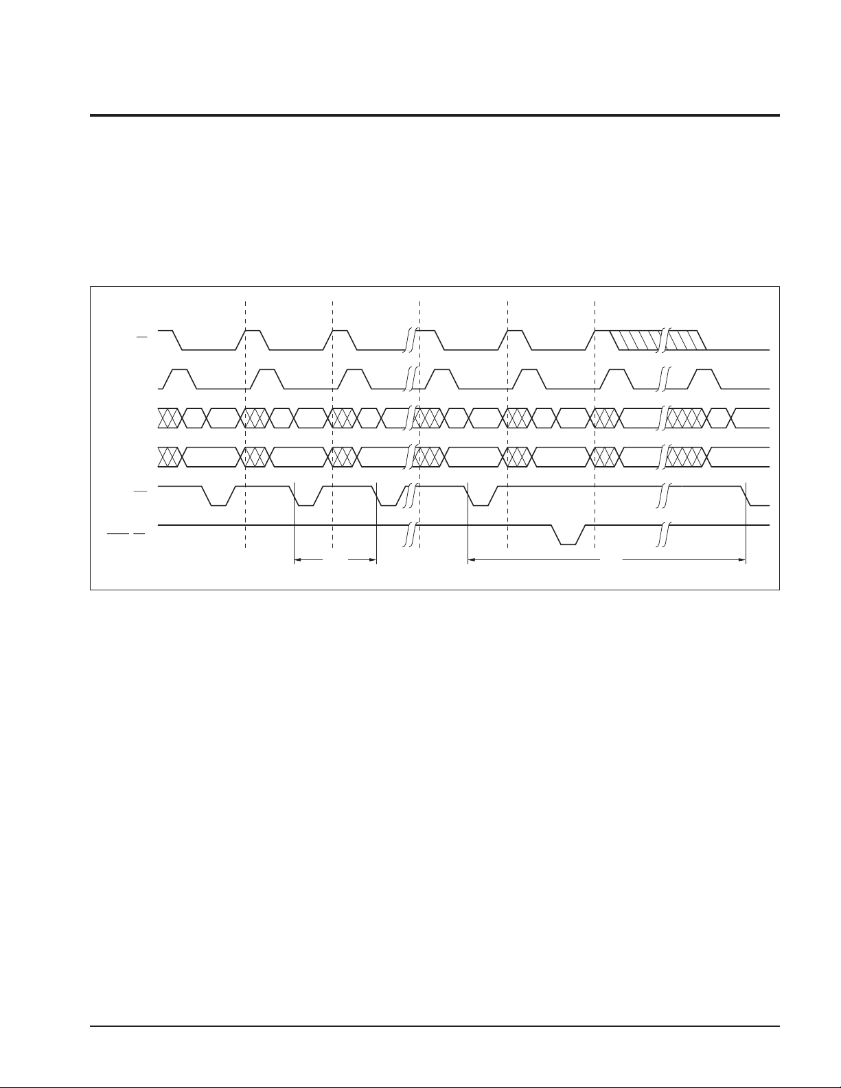
PAGE WRITE OPERATION
Regardless of the microcontroller employed, the X88C64
supports page mode write operations. This allows the
microcontroller to write from one to thirty-two bytes of
data to the X88C64. Each individual write within a page
write operation must conform to the byte write timing
requirements. The falling edge of WR starts a timer
delaying the internal programming cycle 100µs. Therefore, each successive write operation must begin within
100µs of the last byte written. The following waveforms
illustrate the sequence and timing requirements.
Page Write Timing Sequence for WR Controlled Operation
Notes: (1) For each successive write within a page write cycle A5–A12 must be the same.
(2) Although it is not illustrated, the microcontroller may interleave read operations between the individual byte writes within the page
write operation. Two responses are possible:
a. Reading from the same plane being written (A12 of Read = A12 of Write) is effectively a Toggle Bit Polling operation.
b. Reading from the opposite plane being written (A12 of Read ≠ A12 of Write) true data will be returned, facilitating the use of a
single memory component as both program and data storage.
3867 FHD F08
5
 Loading...