XICOR X68257P, X68257JM, X68257JI, X68257J, X68257SM Datasheet
...
X68257
68XX Microcontroller Family Compatible
256K X68257 32,768 x 8 Bit
E2 Micro-Peripheral
FEATURES
• Multiplexed Address/Data Bus
—Direct Interface to Popular 68HC11 Family
• High Performance CMOS
—Fast Access Time, 120ns
—Low Power
—60mA Active Maximum
—500µA Standby Maximum
• Software Data Protection
• Toggle Bit Polling
—Early End of Write Detection
• Page Mode Write
—Allows up to 128 Bytes to be Written in
One Write Cycle
• High Reliability
—Endurance: 10,000 Write Cycle
—Data Retention: 100 Years
• 28-Lead PDIP Package
• 28-Lead SOIC Package
• 32-Lead PLCC Package
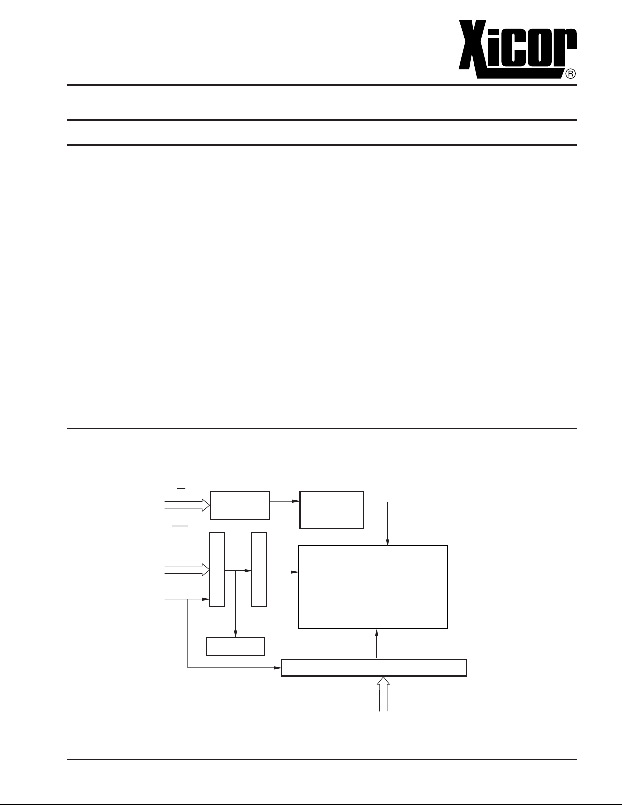
FUNCTIONAL DIAGRAM
DESCRIPTION
The X68257 is an 32K x 8 E2PROM fabricated with
advanced CMOS Textured Poly Floating Gate Technology. The X68257 features a multiplexed address and
data bus allowing direct interface to a variety of popular
single-chip microcontrollers operating in expanded multiplexed mode without the need for additional interface
circuitry.
CE, CE
R/W
E
SEL
A8–A
AS
© Xicor, Inc. 1994, 1995, 1996 Patents Pending Characteristics subject to change without notice
6539-1.7 9/16/96 T0/C1/D2 SH
14
CONTROL
LOGIC
L
A
T
C
H
E
S
Y DECODE
SOFTWARE
DATA
PROTECT
X
D
E
C
O
D
E
I/O & ADDRESS LATCHES AND BUFFERS
1
32K x 8
E2PROM
A/D0–A/D
6539 ILL F02.2
7
X68257
PIN DESCRIPTIONS
Address/Data (A/D0–A/D7)
Multiplexed low-order addresses and data. The addresses flow into the device while AS is HIGH. After AS
transitions from a HIGH to LOW the addresses are
latched. Once the addresses are latched these pins
input data or output data depending on R/W, SEL, and
CE.
Addresses (A8–A14)
High order addresses flow into the device when AS = V
IH
and are latched when AS goes LOW.
Chip Enable (CE)
The Chip Enable input must be LOW to enable all read/
write operations. When CE is HIGH, AS is LOW, and CE
is LOW, the X68257 is placed in the low power standby
mode.
Chip Enable (CE)
Chip Enable is active HIGH. When CE is used to select
the device, the CE must be tied HIGH.
Program Store Enable (SEL)
When the X68257 is to be used in a 68XX-based
system, SEL is tied to VSS.
Read/Write (R/W)
When the X68257 is to be used in a 68XX-based
system, R/W is tied directly to the microcontroller’s R/W
output.
Address Strobe (AS)
Addresses flow through the latches to address decoders
when AS is HIGH and are latched when AS transitions
from a HIGH to LOW.
PIN NAMES
Symbol Description
AS Address Strobe
A/D0–A/D
A8–A
14
7
Address Inputs/Data I/O
Address Inputs
E Enable Input
R/W Read/Write Input
CE, CE Chip Enable
SEL Device Select—Connect to V
V
SS
V
CC
Ground
Supply Voltage
SS
NC No Connect
6539 PGM T01.2
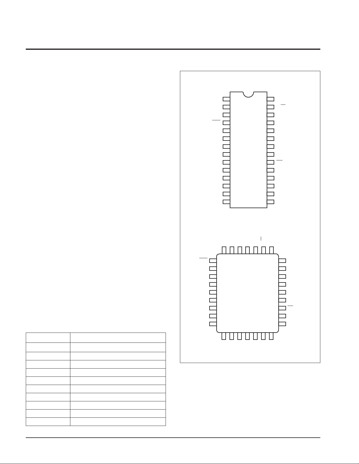
PIN CONFIGURATION
SEL
A/D
A
A
SEL
A/D
A/D
A/D
V
CE
NC
NC
NC
NC
NC
NC
0
1
14
2
12
AS
3
4
CE
5
NC
6
NC
7
NC
8
NC
9
NC
10
11
0
12
1
13
2
14
SS
12
A
AS
3 2 1 32 31
430
5
6
7
8
9
10
11
12
13
15 16 17 18 19
14 20
2
A/D1A/D
PDIP
SOIC
X68257
PLCC
14
A
NC
X68257
SS
NC
V
28
V
27
R/W
26
A
25
A
24
A
23
A
22
E
21
A
20
CE
19
A/D
18
A/D
17
A/D
16
A/D
15
A/D
CC
13
V
A
R/W
29
28
27
26
25
24
23
22
21
5
A/D3A/D4A/D
CC
13
8
9
11
10
7
6
5
4
3
6539 FHD F01.3
A
8
A
9
A
11
NC
E
A
10
CE
A/D
7
A/D
6
6539 FHD F01A.5
2
X68257
PRINCIPLES OF OPERATION
The X68257 is a highly integrated peripheral device for
a wide variety of single-chip microcontrollers. The X68257
provides 32K-bytes of 5V E2PROM which can be used
either for program storage, data storage, or a combination of both, in systems based upon Von Neumann
(68XX) architectures. The X68257 incorporates the
interface circuitry normally needed to decode the control
signals and demultiplex the address/data bus to provide
a “seamless” interface.
The interface inputs on the X68257 are configured such
that it is possible to directly connect them to the proper
interface signals of the appropriate single-chip microcontroller.
The X68257 features the industry standard 5V E2PROM
characteristics such as byte or page mode write and
Toggle Bit Polling.
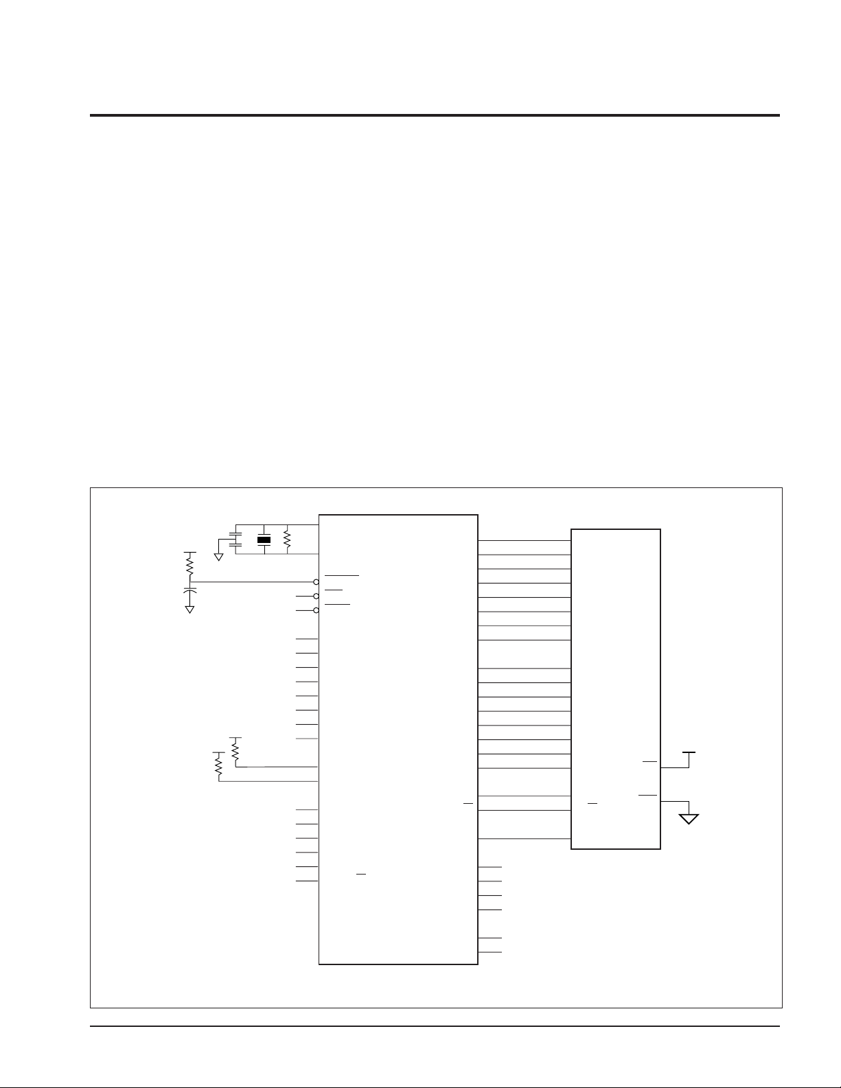
Typical Application
U?
30
XTAL
29
EXTAL
39
RESET
41
IRQ
40
XIRQ
8
PA0
7
PA1
6
PA2
5
PA3
4
PA4
3
PA5
2
PA6
1
PA7
25
MODA
24
MODB
42
PD0
43
PD1
44
45
46
47
PD2
PD3
PD4
PD5
68HC11
MISO
MOSI
SCK
SS
DEVICE OPERATION
Motorola 68XX operation requires the microcontroller
AS, E, and R/W outputs to be tied to the X68257 AS, E,
and R/W inputs respectively.
The falling edge of AS will latch the addresses for both
a read and write operation. The state of the R/W output
determines the operation to be performed, with the E
signal acting as a data strobe.
If R/W is HIGH and CE is HIGH (read operation) data will
be output on A/D0–A/D7 after E transitions HIGH. If
R/W is LOW and CE is HIGH (write operation) data
present at A/D0–A/D7 will be strobed into the X68257 on
the HIGH to LOW transition of E.
U?
PC0
PC1
PC2
PC3
PC4
PC5
PC6
PC7
PB0
PB1
PB2
PB3
PB4
PB5
PB6
PB7
AS
R/W
PE0
PE1
PE2
PE3
VRH
VRL
31
32
33
34
35
36
37
38
16
15
14
13
12
11
10
9
26
28
27
E
17
18
19
20
22
21
11
12
12
15
16
17
18
19
25
24
21
23
26
27
22
2
1
5
3
A/D0
A/D1
A/D2
A/D3
A/D4
A/D5
A/D6
A/D7
A8
A9
A10
A11
A12
A13
A14
CE
AS
R/W
E
X68257
20
CE
SEL
6539 ILL F03.2
VCC
4
3
X68257
MODE SELECTION
CE E R/W Mode I/O Power
V
SS
X X Standby High Z Standby (CMOS)
LOW X X Standby High Z Standby (TTL)
HIGH HIGH HIGH Read D
HIGH LOW Write D
OUT
IN
Active
Active
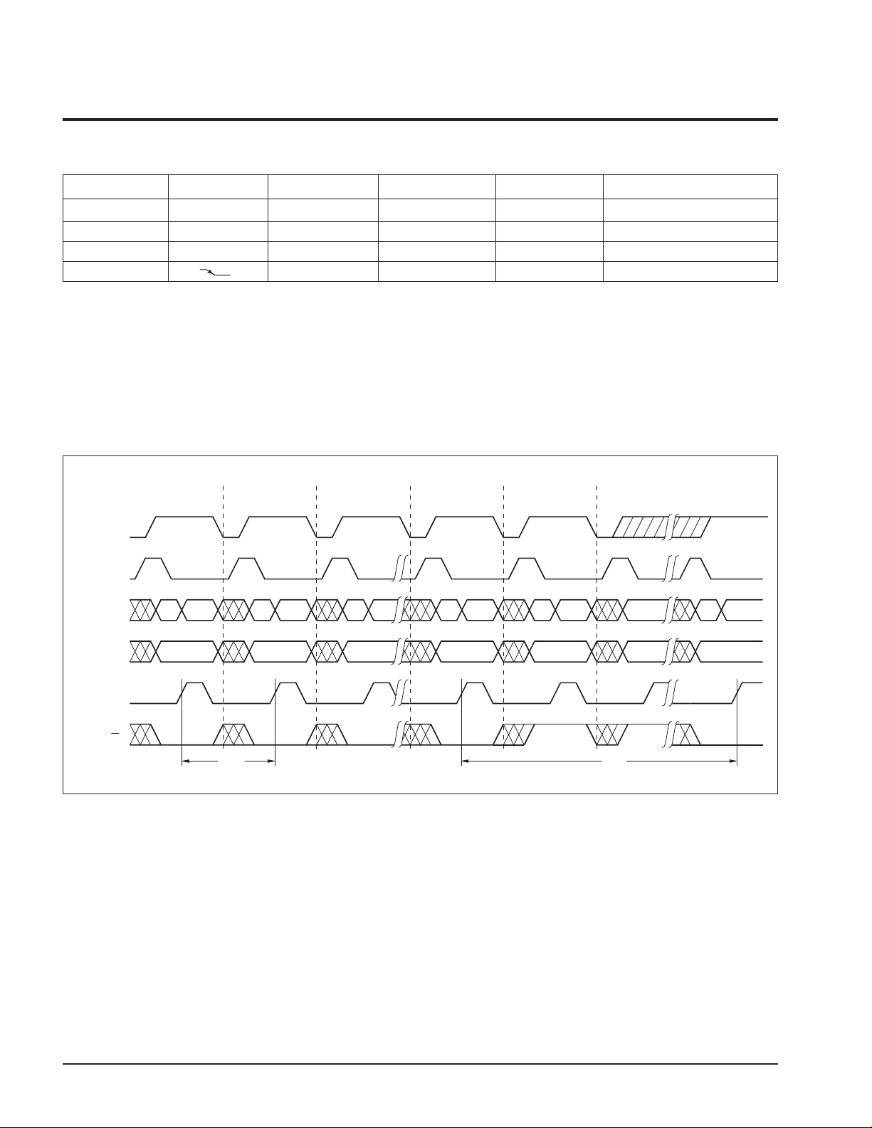
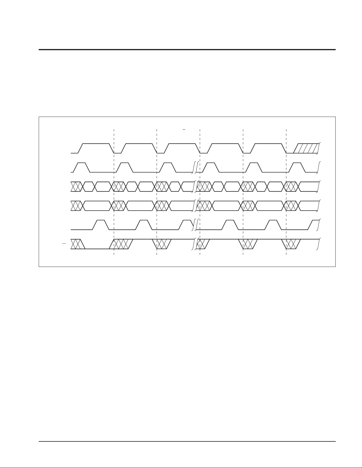
PAGE WRITE OPERATION
Regardless of the microcontroller employed, the X68257
supports page mode write operations. This allows the
microcontroller to write from 1 to 128 bytes of data to the
X68257. Each individual write within a page write operation must conform to the byte write timing requirements.
The rising edge of E starts a timer delaying the internal
programming cycle 100µs. Therefore, each successive
write operation must begin within 100µs of the last byte
written. The following waveforms illustrate the sequence
and timing requirements.
Page Write Timing Sequence for E Controlled Operation
OPERATION
CE
AS
A/D0–A/D
7
BYTE 0
A
IN
D
IN
BYTE 1
A
IN
BYTE 2 LAST BYTE READ (1)(2) AFTER tWC READY FOR
D
IN
A
D
IN
IN
A
D
IN
IN
A
D
IN
IN
NEXT WRITE OPERATION
A
6539 PGM T02.2
IN
A
IN
A8–A
14
E
R/W
An
t
BLC
Note: (1) For each successive write within a page write cycle A7–A14 must be the same.
t
WC
ADDR
Next AddressAn An An An
6539 FHD F07.1
4
X68257
Toggle Bit Polling
Because the typical write timing is less than the specified
5ms, Toggle Bit Polling has been provided to determine
the early end of write. During the internal programming
cycle I/O6 will toggle from “1” to “0” and “0” to “1” on
Toggle Bit Polling E Control
OPERATION
CE
AS
A/D0–A/D
A8–A
7
14
E
LAST BYTE
WRITTEN
A
D
IN
An
I/O6=XI/O6=X
A
D
IN
IN
OUT
An An An An
A
IN
subsequent attempts to read the device. When the
internal cycle is complete, the toggling will cease and the
device will be accessible for additional read or write
operations.
D
OUT
I/O6=X
A
IN
D
OUT
I/O6=X X68257 READY FOR
A
D
IN
OUT
NEXT OPERATION
A
ADDR
IN
R/W
6539 FHD F08.2
5
 Loading...