

Advanced 2-Wire Serial E
2
PROM with Block Lock
TM
Protection
32K
4096 x 8 Bit
Preliminary Information
Xicor, 1995, 1996 Patents Pending
6552-2.4 5/13/96 T1/C10/D0 NS
1
Characteristics subject to change without notice
X24325
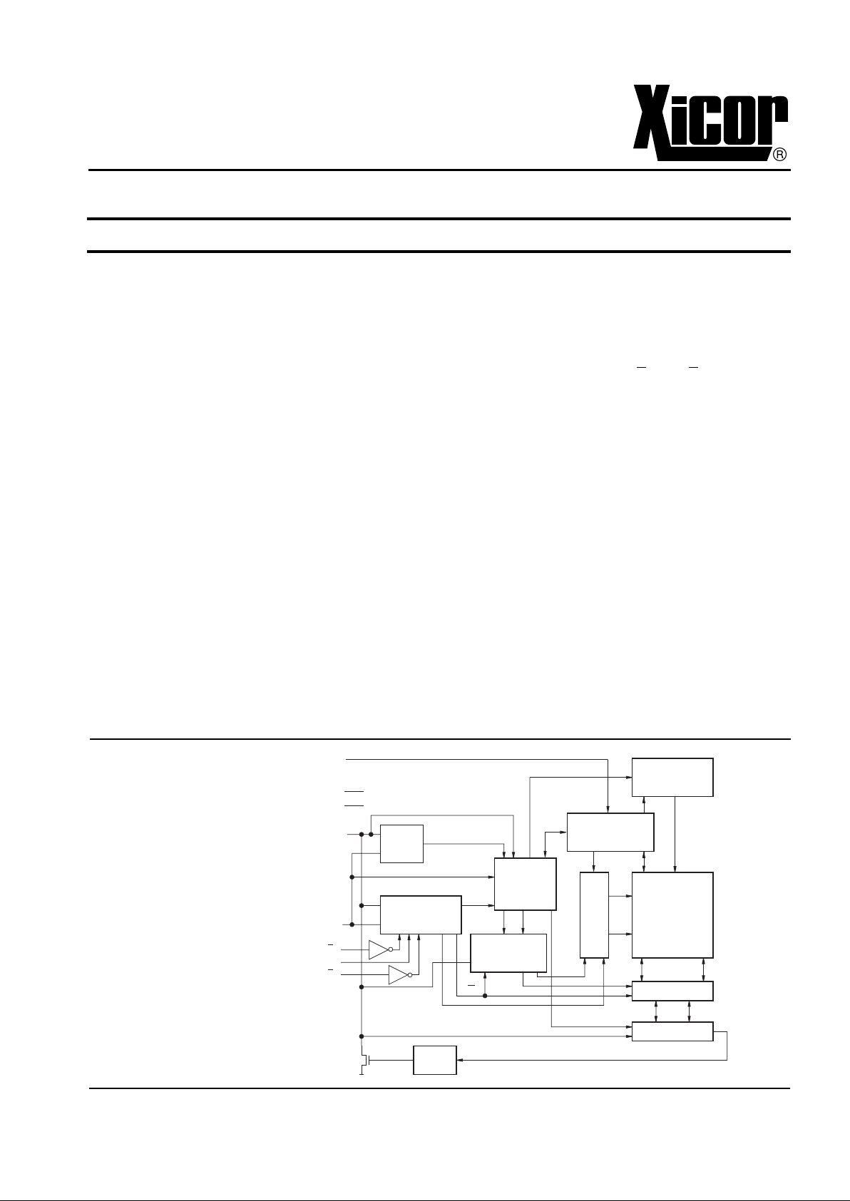
FUNCTIONAL DIAGRAM
FEATURES
•
2.7V to 5.5V Power Supply
•
Low Power CMOS
—Active Read Current Less Than 1mA
—Active Write Current Less Than 3mA
—Standby Current Less Than 1 µ A
•
Internally Organized 4096 x 8
•
New Programmable Block Lock Protection
—Software Write Protection
—Programmable hardware Write Protect
•
Block Lock (0, 1/4, 1/2, or all of the E
2
PROM
array)
•
2 Wire Serial Interface
•
Bidirectional Data Transfer Protocol
•
32 Byte Page Write Mode
—Minimizes T otal Write Time Per Byte
•
Self Timed Write Cycle
—Typical Write Cycle Time of 5ms
•
High Reliability
—Endurance: 100,000 Cycles
—Data Retention: 100 Years
•
Available Packages
—8-Lead PDIP
—8-Lead SOIC (JEDEC)
—14-Lead TSSOP
DESCRIPTION
The X24325 is a CMOS 32,768 bit serial E
2
PROM,
internally organized 4096 x 8. The X24325 features a
serial interface and software protocol allowing operation on a simple two wire bus.
Three device select inputs (S
0
, S
1
, S
2
) allow up to
eight devices to share a common two wire bus .
A Write Protect Register at the highest address loca-
tion, FFFh, provides three new write protection
features: Software Write Protect, Block Write Protect,
and Hardware Write Protect. The Software Write
Protect feature prevents any nonvolatile writes to the
X24325 until the WEL bit in the write protect register is
set. The Block Write Protection feature allows the user
to individually write protect four blocks of the array by
programming two bits in the write protect register. The
Programmable Hardware Write Protect feature allows
the user to install the X24325 with WP tied to V
CC
,
program the entire memory array in place, and then
enable the hardware write protection by programming
a WPEN bit in the write protect register. After this,
selected blocks of the array, including the write protect
register itself, are permanently write protected.
Xicor E
2
PROMs are designed and tested for applications requiring extended endurance. Inherent data
retention is greater than 100 years.
START
STOP
LOGIC
CONTROL
LOGIC
SLAVE ADDRESS
REGISTER
+COMPARA TOR
H.V. GENERATION
TIMING &
CONTROL
WORD
ADDRESS
COUNTER
XDEC
YDEC
D
OUT
ACK
E
2
PROM
128 X 256
DATA REGISTER
START CYCLE
V
CC
R/W
PIN
V
SS
SDA
SCL
S
0
S
1
D
OUT
LOAD INC
CK
8
6552 ILL F01.1
WRITE PROTECT
REGISTER AND
LOGIC
WP
S
2
X24325
2
PIN DESCRIPTIONS
Serial Clock (SCL)
The SCL input is used to clock all data into and out of
the device.
Serial Data (SDA)
SDA is a bidirectional pin used to transfer data into
and out of the device. It is an open drain output and
may be wire-ORed with any number of open drain or
open collector outputs.
An open drain output requires the use of a pull-up
resistor. For selecting typical values, refer to the PullUp Resistor selection graph at the end of this data
sheet.
Device Select (S
0
, S
1
, S
2
)
The device select inputs (S
0
, S
1
, S
2
) are used to set
the first three bits of the 8-bit slave address. This
allows up to eight X24325’s to share a common bus.
These inputs can be static or actively driven. If used
statically they must be tied to V
SS
or V
CC
as appropriate. If actively driven, they must be driven with
CMOS levels (driven to V
CC
or V
SS
).
Write Protect (WP)
The write protect input controls the hardware write
protect feature. When held LOW, hardware write
protection is disabled and the X24325 can be written
normally. When this input is held HIGH, and the WPEN
bit in the write protect register is set HIGH, write
protection is enabled, and nonvolatile writes are
disabled to the selected blocks as well as the write
protect register itself.
PIN NAMES
6552 FRM T01.1
Symbol Description
S
0
, S
1
, S
2
Device Select Inputs
SDA Serial Data
SCL Serial Clock
WP Write Protect
V
SS
Ground
V
CC
Supply Voltage
NC No Connect
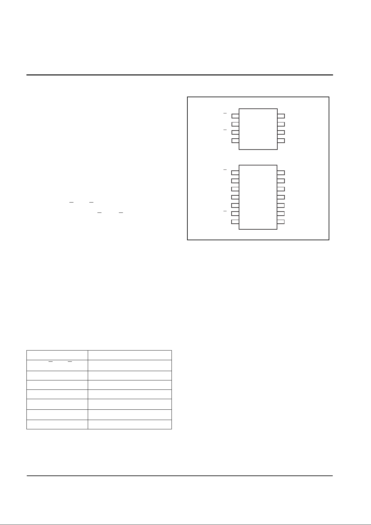
PIN CONFIGURATIONS
6552 ILL F02.5
S
0
S
1
NC
NC
NC
S
2
V
SS
1
2
3
4
5
6
7
14
13
12
11
10
9
8
VCC
WP
NC
NC
NC
SCL
SDA
X24325
14-LEAD TSSOP
VCC
WP
SCL
SDA
S
0
S
1
S
2
VSS
1
2
3
4
8
7
6
5
X24325
8-LEAD DIP & SOIC
X24325
3
DEVICE OPERATION
The X24325 supports a bidirectional bus oriented protocol. The protocol defines any device that sends data
onto the bus as a transmitter, and the receiving device
as the receiver. The device controlling the transfer is a
master and the device being controlled is the slave.
The master will always initiate data transfers, and provide the clock for both transmit and receive operations.
Therefore, the X24325 will be considered a slave in all
applications.
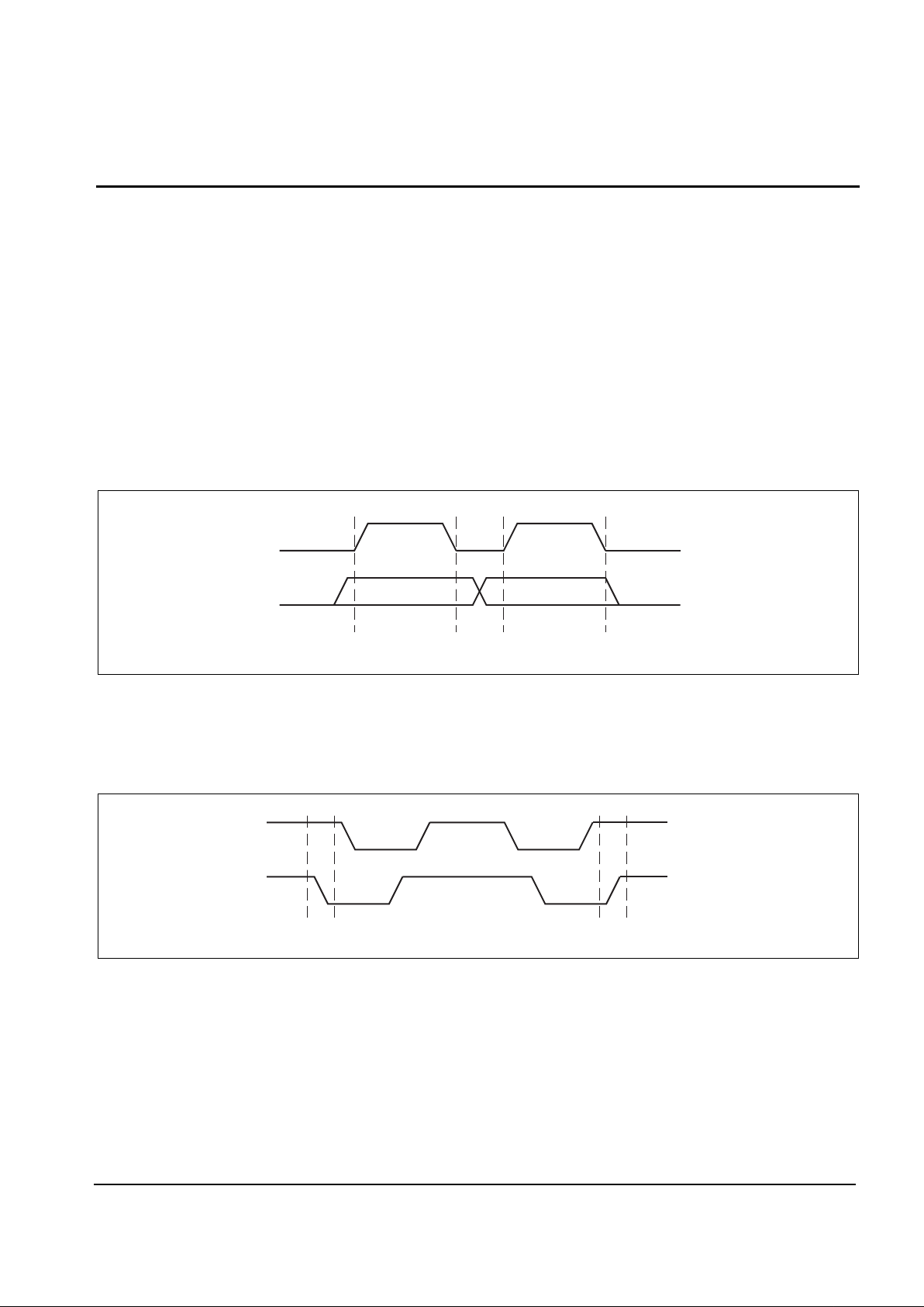
Clock and Data Conventions
Data states on the SDA line can change only during
SCL LOW. SDA state changes during SCL HIGH are
reserved for indicating start and stop conditions. Refer
to Figures 1 and 2.
Start Condition
All commands are preceded by the start condition,
which is a HIGH to LOW transition of SDA when SCL is
HIGH. The X24325 continuously monitors the SDA and
SCL lines for the start condition and will not respond to
any command until this condition has been met.
SCL
SDA
DATA STABLE DATA
CHANGE
6552 ILL F04
SCL
SDA
START BIT STOP BIT
6552 ILL F05
Figure 1. Data Validity
Figure 2. Definition of Start and Stop
Notes: (5) Typical values are for T
A
= 25 ° C and nominal supply voltage (5V)
(6) t
WR
is the minimum cycle time from the system perspective when polling techniques are not used. It is the maximum time the
device requires to perform the internal write operation.
X24325
4
Figure 3. Acknowledge Response From Receiver
Stop Condition
All communications must be terminated by a stop
condition, which is a LOW to HIGH transition of SDA
when SCL is HIGH. The stop condition is also used to
place the device into the standby power mode after a
read sequence. A stop condition can only be issued
after the transmitting device has released the bus .
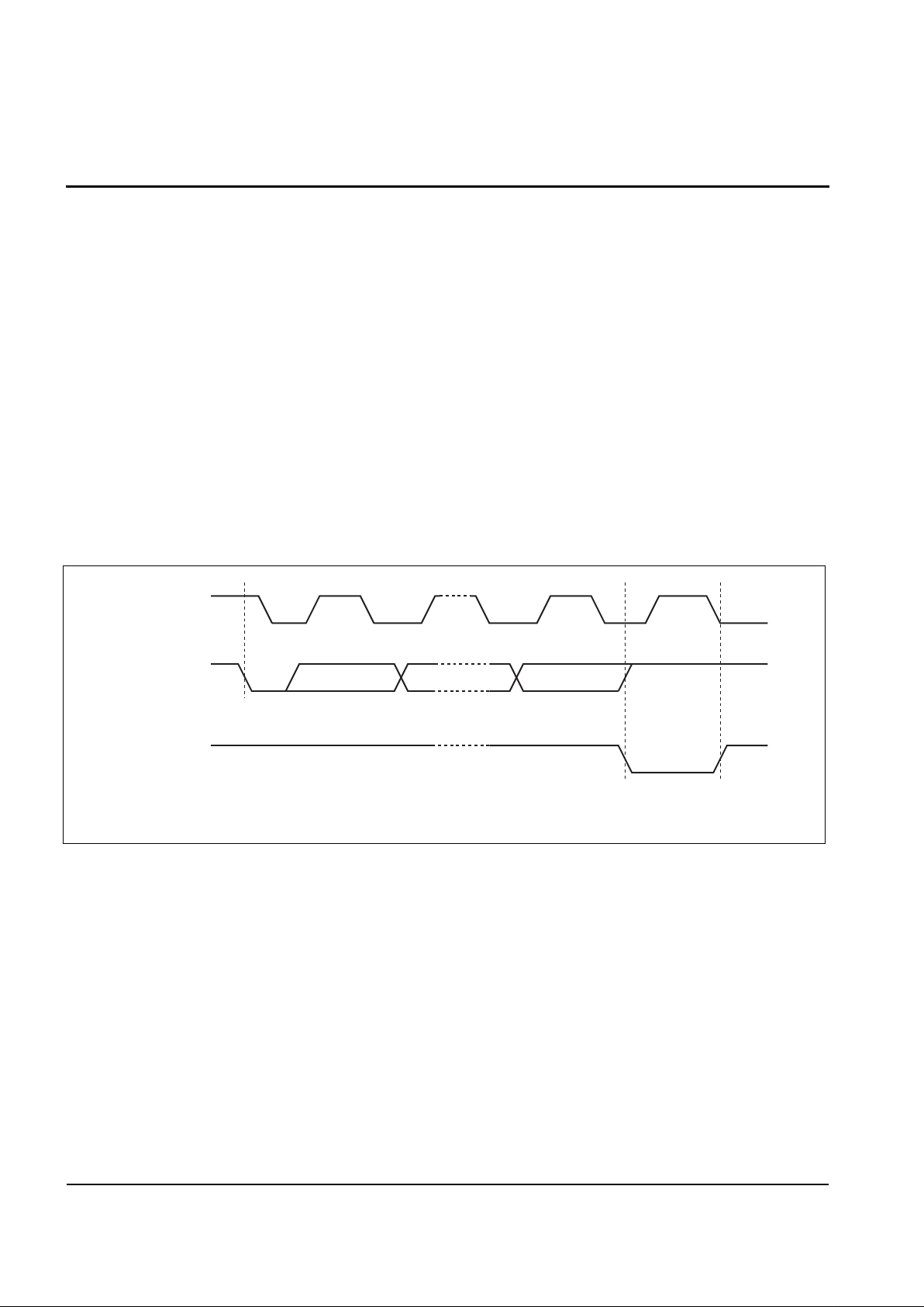
Acknowledge
Acknowledge is a software con v ention used to indicate
successful data transfer. The transmitting device,
either master or slave, will release the bus after transmitting eight bits. During the ninth clock cycle the
receiver will pull the SDA line LOW to acknowledge
that it received the eight bits of data. Ref er to Figure 3.
The X24325 will respond with an acknowledge after
recognition of a start condition and its slave address. If
both the device and a write operation have been
selected, the X24325 will respond with an acknowledge after the receipt of each subsequent eight-bit
word.
In the read mode the X24325 will transmit eight bits of
data, release the SDA line and monitor the line for an
acknowledge. If an acknowledge is detected and no
stop condition is generated by the master, the X24325
will continue to transmit data. If an acknowledge is not
detected, the X24325 will terminate further data transmissions. The master must then issue a stop condition
to return the X24325 to the standby power mode and
place the device into a known state.
6552 ILL F06
SCL FROM
MASTER
DATA OUTPUT
FROM
TRANSMITTER
1
8 9
DATA
OUTPUT
FROM
RECEIVER
START
ACKNOWLEDGE
X24325
5
Figure 5. Byte Write
BUS ACTIVITY:
MASTER
SDA LINE
BUS ACTIVITY:
X24325
S
T
A
R
T
SLAVE
ADDRESS
S
S
T
O
P
P
A
C
K
A
C
K
A
C
K
WORD
ADDRESS DATA
6552 ILL F08
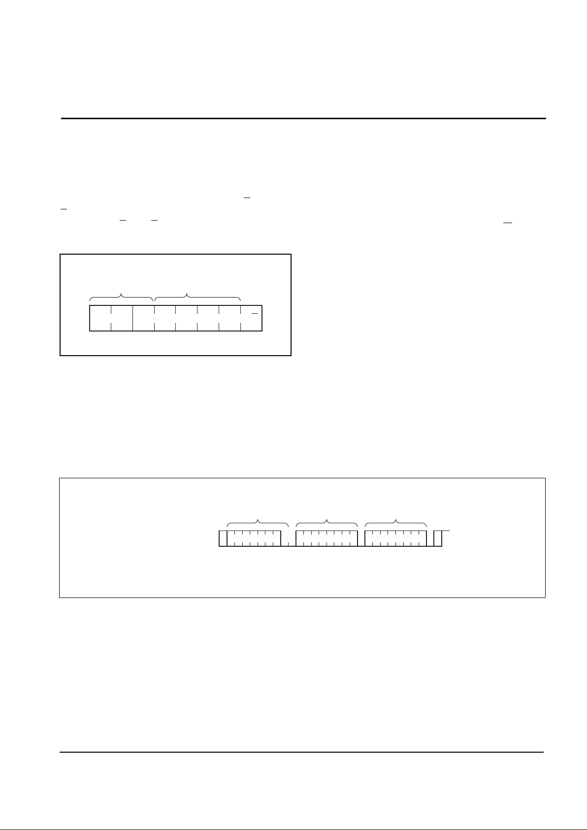
DEVICE ADDRESSING
Following a start condition the master must output the
address of the slave it is accessing (see Figure 4). The
next three bits are the device select bits. A system
could have up to eight X24325’s on the bus. The eight
addresses are defined by the state of the S
0
, S
1
and
S
2
inputs. S
0
and S
2
of the slave address must be the
inverse of the S
0
and S
2
input pins.
Figure 4. Slave Address
The next four bits of the slave address are an extension of the array’s address and are concatenated with
the eight bits of address in the word address field,
providing direct access to the whole 4096 x 8 array.
6552 ILL F07.2
S
2
A9 A8 R/W
DEVICE
SELECT
S1S
0
HIGH ORDER
WORD
ADDRESS
A11
A10
The last bit of the slave address defines the operation to
be performed. When set HIGH a read operation is
selected, when set LOW a write operation is selected.
Following the start condition, the X24325 monitors the
SDA bus comparing the slave address being transmitted
with its slave address device type identifier. Upon a
correct compare the X24325 outputs an acknowledge on
the SDA line. Depending on the state of the R/W
bit, the
X24325 will execute a read or write operation.
WRITE OPERATIONS
Byte Write
For a write operation, the X24325 requires a second address field. This address field is the word address, comprised of eight bits, providing access to any one of 4096
words in the array. Upon receipt of the word address, the
X24325 responds with an acknowledge and awaits the
next eight bits of data, again responding with an acknowledge. The master then terminates the transfer by generating a stop condition, at which time the X24325 begins
the internal write cycle to the nonvolatile memory. While
the internal write cycle is in progress the X24325 inputs
are disabled, and the device will not respond to any requests from the master. Refer to Figure 5 for the address,
acknowledge and data transfer sequence.
X24325
6
Figure 6. Page Write
Page Write
The X24325 is capable of a 32 byte page write operation. It is initiated in the same manner as the byte write
operation, but instead of terminating the write cycle after the first data word is transferred, the master can
transmit up to fifteen more words. After the receipt of
each word, the X24325 will respond with an acknowledge.
After the receipt of each word, the five low order address bits are internally incremented by one. The high
order bits of the word address remain constant. If the
master should transmit more than 32 words prior to
generating the stop condition, the address counter will
“roll over” and the previously written data will be overwritten. As with the byte write operation, all inputs are
disabled until completion of the internal write cycle. Refer to Figure 6 for the address, acknowledge and data
transfer sequence.
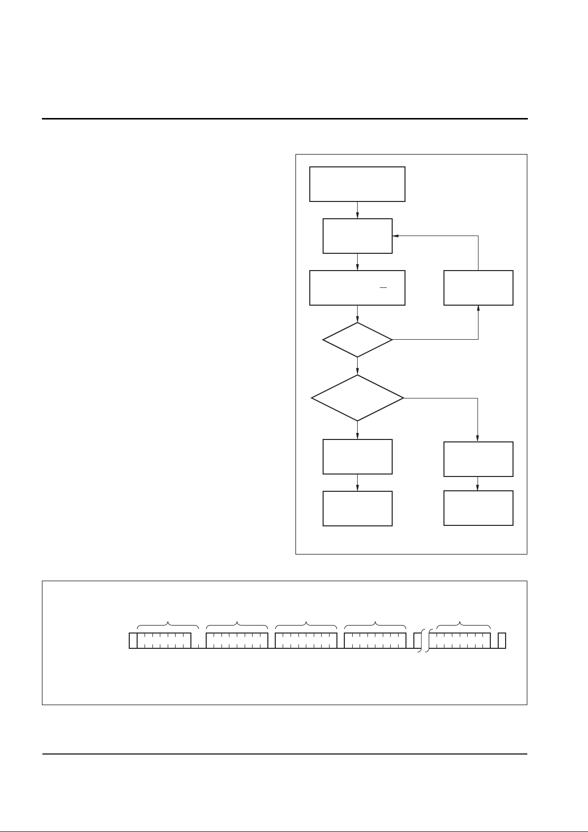
Acknowledge Polling
The Max Write Cycle Time can be significantly reduced
using Acknowledge Polling. To initiate Acknowledge
Polling, the master issues a start condition followed by
the Slave Address Byte for a write or read operation. If
the device is still busy with the high voltage cycle, then
no ACK will be returned. If the device has completed
the write operation, an ACK will be returned and the
host can then proceed with the read or write operation.
Refer to Flow 1.
Flow 1. ACK Polling Sequence
6552 ILL F09
WRITE OPERATION
COMPLETED
ENTER ACK POLLING
ISSUE
START
ISSUE SLAVE
ADDRESS AND R/W = 0
ACK
RETURNED?
NEXT
OPERATION
A WRITE?
ISSUE BYTE
ADDRESS
PROCEED
ISSUE STOP
NO
YES
YES
PROCEED
ISSUE STOP
NO
BUS ACTIVITY:
MASTER
SDA LINE
BUS ACTIVITY:
X24325
S
T
A
R
T
SLAVE
ADDRESS
S
S
T
O
P
P
A
C
K
A
C
K
A
C
K
A
C
K
A
C
K
WORD ADDRESS (n) DATA n DATA n+1 DATA n+31
6552 ILL F10.1

X24325
7
Figure 7. Current Address Read
Figure 8. Random Read
READ OPERATIONS
Read operations are initiated in the same manner as
write operations with the exception that the R/W bit of
the slave address is set HIGH. There are three basic
read operations: current address read, random read
and sequential read.
It should be noted that the ninth clock cycle of the read
operation is not a “don’t care.” To terminate a read operation, the master must either issue a stop condition
during the ninth cycle or hold SDA HIGH during the
ninth clock cycle and then issue a stop condition.
Current Address Read
Internally the X24325 contains an address counter that
maintains the address of the last word read, incremented by one or the exact address of the last word written.
Therefore, if the last access read was to address n, the
next read operation would access data from address
n + 1. Upon receipt of the slave address with the R/W
set HIGH, the X24325 issues an acknowledge and
transmits the eight-bit word. The read operation is ter-
minated by the master; by not responding with an acknowledge and by issuing a stop condition. Refer to
Figure 7 for the sequence of address, acknowledge
and data transfer.
Random Read
Random read operations allow the master to access
any memory location in a random manner. Prior to issuing the slave address with the R/W bit set HIGH, the
master must first perform a “dummy” write operation.
The master issues the start condition, and the slave address with the R/W bit set LOW, followed by the word
address it is to read. After the word address acknowledge, the master immediately reissues the start condition and the slave address with the R/W
bit set HIGH.
This will be followed by an acknowledge from the
X24325 and then by the eight-bit word. The read operation is terminated by the master; by not responding
with an acknowledge and by issuing a stop condition.
Refer to Figure 8 for the address, acknowledge and
data transfer sequence.
BUS ACTIVITY:
MASTER
SDA LINE
BUS ACTIVITY:
X24325
S
T
A
R
T
SLAVE
ADDRESS
S
S
T
O
P
P
A
C
K
DATA
6552 ILL F11
BUS ACTIVITY:
MASTER
SDA LINE
BUS ACTIVITY:
X24325
S
T
A
R
T
SLAVE
ADDRESS
S
A
C
K
6552 ILL F12.1
S
T
A
R
T
S
WORD
ADDRESS n
A
C
K
SLAVE
ADDRESS
DATA n
A
C
K
S
T
O
P
P

X24325
8
Figure 10. Typical System Configuration
Sequential Read
Sequential reads can be initiated as either a current
address read or random access read. The first word is
transmitted as with the other modes, however, the
master now responds with an acknowledge, indicating
it requires additional data. The X24325 continues to
output data for each acknowledge received. The read
operation is terminated by the master; by not
responding with an acknowledge and then issuing a
stop condition.
The data output is sequential, with the data from
address n followed by the data from n + 1. The address
counter for read operations increments all address bits,
allowing the entire memory contents to be serially read
during one operation. At the end of the address space
(address 4095), the counter “rolls over” to 0 and the
X24325 continues to output data for each acknowledge
received. Refer to Figure 9 for the address,
acknowledge and data transfer sequence.
BUS ACTIVITY:
MASTER
SDA LINE
BUS ACTIVITY:
X24325
SLAVE
ADDRESS
A
C
K
6552 ILL F13
A
C
K
DATA n+x
S
T
O
P
P
DATA n
A
C
K
DATA n+1
A
C
K
DATA n+2
MASTER
TRANSMITTER/
RECEIVER
SLAVE
RECEIVER
SLAVE
TRANSMITTER/
RECEIVER
MASTER
TRANSMITTER
MASTER
TRANSMITTER/
RECEIVER
PULL-UP
RESISTORS
SDA
SCL
V
CC
6552 ILL F14
Figure 9. Sequential Read

X24325
9
WRITE PROTECT REGISTER
The Write Protect Register (WPR) is located at the
highest address, FFFh.
Figure 11. Write Protect Register
WPR.1 = WEL
– Write Enable Latch (Volatile)
0 = Write enable latch reset, writes disabled
1 = Write enable latch set, writes enabled
If WEL = 0 then “no ACK” after first b yte of input data.
WPR.2 = RWEL
– Register Write Enable Latch (Volatile)
0 = Register write enable latch reset, writes dis-
abled
1 = Register write enable latch set, writes enabled
WPR.3, WPR.4 = BP0, BP1
– Block Protect Bits (Nonvolatile)
(See Block Protect section for definition)
WPR.7 = WPEN
– Write Protect Enable Bit (Nonvolatile)
(See Hardware Write Protect section for definition)
Writing to the Write Protect Register
The Write Protect Register is written by performing a
random write of one byte directly to address, FFFh. If a
page write is performed starting with any address
other than FFFh, the byte in the array at address FFFh
will be written instead of the Write Protect Register
(assuming writes are not disabled by the block protect
register).
The state of the Write Protect Register can be read by
performing a random read at address FFFh at any
time. If a sequential read starting at any other address
than FFFh is performed, the contents of the byte in the
array at FFFh is read out instead of the Write Protect
Register.
7 6 5 4 3
2
1
0
WPEN 0 0 BP1 BP0
RWEL
WEL
0
6552 ILL F15
WPR (Addr = FFFh)
WEL and RWEL are volatile latches that power-up in
the LOW (disabled) state. A write to any address other
than FFFh, where the Write Protect Register is
located, will be ignored (no ack) until the WEL bit is set
HIGH. The WEL bit is set by writing 0000001x to
address FFFh. Once set, WEL remains HIGH until
either reset (by writing 00000000 to FFFh) or until the
part powers-up again. The RWEL bit controls writes to
the block protect bits. RWEL is set by first setting WEL
= 1 and then writing 0000011x to address FFFh.
RWEL must be set in order to change the bloc k protect
bits, BP0 and BP1, or the WPEN bit. RWEL is reset
when the block protect or WPEN bits are changed, or
when the part powers-up again.
Programming the BP or WPEN Bits
A three step sequence is required to change the
nonvoltaile Block Protect or Write Protect Enable:
1) Set WEL = 1 (write 00000010 to address FFFh,
volatile write cycle)
(Start)
2) Set RWEL = 1 (write 00000110 to address FFFh,
volatile write cycle)
(Start)
3) Set BP1, BP0, and/or WPEN bits (Write w00yz010
to address FFFh)
w = WPEN, y = BP1, Z = BP0,
(Stop)
Step 3 is a nonvolatile write cycle, requiring 10ms to
complete. RWEL is reset (0) by this write cycle,
requiring another write cycle to set RWEL again before
the block protect bits can be changed. RWEL must be
0 in step 3; if w00yz110 is written to address FFFh,
RWEL is set but WPEN, BP1 and BP0 are not
changed (the device remains at step 2).

X24325
10
Block Protect Bits
The Block Protect Bits BP0 and BP1 determine which
blocks of the memory are write-protected:
Programmable Hardware Write Protect
The Write Protect (WP) pin and the Write Protect
Enable (WPEN) bit in the Write Protect Register
control the programmable hardware write protect
feature. Hardware write protection is enabled when the
WP pin and the WPEN bit are both HIGH, and
disabled when either the WP pin is LOW or the WPEN
bit is LOW. When the chip is hardware write-protected,
nonvolatile writes are disabled to the Write Protect
Register, including the BP bits and the WPEN bit itself,
as well as to block-protected sections in the memory
array. Only the sections of the memory array that are
not block-protected can be written. Note that since the
WPEN bit is write-protected, it cannot be changed
back to a LOW state, and write protection is disabled
as long as the the WP pin is held HIGH. Table 2
defines the write protection status for each state of
WPEN and WP.
Table 1. Block Protect Bits
6552 FRM T02
BP1 BP0
Protected
Addresses
0 0 None
0 1 C00h–FFFh Upper 1/4
1 0 800h–FFFh Upper 1/2
1 1 0000h–FFFh
Full Array (WPR
not included)
Table 2. Write Protect Status Table
6552 FRM T03
WP WPEN
Memory Array
(Not Block
Protected)
Memory Array
(Block Protected) BP Bits WPEN Bit
0 X Writable Protected Writable Writable
X 0 Writable Protected Writable Writable
1 1 Writable Protected Protected Protected

X24325
11
ABSOLUTE MAXIMUM RATINGS*
Temperature Under Bias
X24325.......................................–65 ° C to +135
°C
Storage Temperature........................–65°C to +150°C
Voltage on any Pin with
Respect to V
SS
....................................–1V to +7V
D.C. Output Current..............................................5mA
Lead Temperature (Soldering, 10 Seconds)......300°C
*COMMENT
Stresses above those listed under “Absolute Maximum
Ratings” may cause permanent damage to the device.
This is a stress rating only and the functional operation
of the device at these or any other conditions above
those indicated in the operational sections of this
specification is not implied. Exposure to absolute
maximum rating conditions for extended periods may
affect device reliability.
D.C. OPERATING CHARACTERISTICS
6552 FRM T06.1
CAPACITANCE TA = +25°C, f = 1MHz, VCC = 5V
6552 FRM T07.1
Notes: (1) Must perform a stop command prior to measurement.
(2) VIL min. and VIH max. are f or ref erence only and are not 100% tested.
(3) This parameter is periodically sampled and not 100% tested.
Limits
Symbol Parameter Min. Max. Units Test Conditions
I
CC1
VCC Supply Current (Read) 1 mA SCL = VCC X 0.1/VCC X 0.9 Levels
@ 100KHz, SDA = Open, All Other
Inputs = VSS or VCC – 0.3V
I
CC2
VCC Supply Current (Write) 3 mA
I
SB1
(1)
VCC Standby Current 50 µA SCL = SDA = VCC, All Other
Inputs =
V
SS
or VCC – 0.3V,
V
CC
= 5V ± 10%
I
SB2
(1)
VCC Standby Current 1 µA SCL = SDA = VCC, All Other
Inputs =
V
SS
or VCC – 0.3V,
V
CC
= 2.7V
I
LI
Input Leakage Current 10 µA
V
IN
= VSS to V
CC
I
LO
Output Leakage Current 10 µA
V
OUT
= VSS to V
CC
V
lL
(2)
Input LOW Voltage –1 VCC x 0.3 V
V
IH
(2)
Input HIGH Voltage VCC x 0.7 VCC + 0.5 V
V
OL
Output LOW Voltage 0.4 V IOL = 3mA, VCC = 4.5V
Symbol Parameter Max. Units Test Conditions
C
I/O
(3)
Input/Output Capacitance (SDA) 8 pF V
I/O
= 0V
C
IN
(3)
Input Capacitance (S1, S2, SCL)
6 pF V
IN
= 0V
RECOMMENDED OPERATING CONDITIONS
6552 FRM T04
Temperature Min. Max.
Commercial 0°C +70°C
Industrial –40°C +85°C
Military –55°C +125°C
6552 FRM T05
Supply Voltage Limits
X24325 4.5V to 5.5V
X24325-2.7 2.7V to 5.5V

X24325
12
A.C. OPERATING CHARACTERISTICS (Over the recommended operating conditions, unless otherwise specified.)
Read & Write Cycle Limits
6552 FRM T09.1
POWER-UP TIMING
(4)
6552 FRM T10
Notes: (4) t
PUR
and t
PUW
are the delays required from the time VCC is stable until the specified operation can be initiated. These par ameters
are periodically sampled and not 100% tested.
Symbol Parameter Min. Max. Units
f
SCL
SCL Clock Frequency 0 100 KHz
T
I
Noise Suppression Time
Constant at SCL, SDA Inputs
100 ns
t
AA
SCL LOW to SDA Data Out Valid 0.3 3.5 µs
t
BUF
Time the Bus Must Be Free Before a
New Transmission Can Start
4.7 µs
t
HD:STA
Start Condition Hold Time 4 µs
t
LOW
Clock LOW Period 4.7 µs
t
HIGH
Clock HIGH Period 4 µs
t
SU:STA
Start Condition Setup Time
(for a Repeated Start Condition)
4.7 µs
t
HD:DAT
Data In Hold Time 0 µs
t
SU:DAT
Data In Setup Time 250 ns
t
R
SDA and SCL Rise Time 1 µs
t
F
SDA and SCL Fall Time 300 ns
t
SU:STO
Stop Condition Setup Time 4.7 µs
t
DH
Data Out Hold Time 300 ns
Symbol Parameter Max. Units
t
PUR
Power-up to Read Operation 1 ms
t
PUW
Power-up to Write Operation 5 ms
A.C. CONDITIONS OF TEST
6552 FRM T08.1
Input Pulse Levels VCC x 0.1 to VCC x 0.9
Input Rise and
Fall Times 10ns
Input and Output
Timing Levels
V
CC
X 0.5
EQUIVALENT A.C. LOAD CIRCUIT
6552 ILL F16
5V
1533Ω
100pF
OUTPUT

X24325
13
SYMBOL TABLE
WAVEFORM
INPUTS
OUTPUTS
Must be
steady
Will be
steady
May change
from LOW
to HIGH
Will change
from LOW
to HIGH
May change
from HIGH
to LOW
Will change
from HIGH
to LOW
Don’t Care:
Changes
Allowed
Changing:
State Not
Known
N/A
Center Line
is High
Impedance
The write cycle time is the time from a valid stop
condition of a write sequence to the end of the internal
erase/program cycle. During the write cycle, the
X24325 bus interface circuits are disabled, SDA is
allowed to remain HIGH, and the device does not
respond to its slave address.
Bus Timing
6552 ILL F17
t
SU:STA
t
HD:STAtHD:DAT
t
SU:DAT
t
LOW
t
SU:STO
t
R
t
BUF
SCL
SDA IN
SDA OUT
t
DH
t
AA
t
F
t
HIGH
Write Cycle Limits
6552 FRM T11.1
Symbol Parameter Min. Typ.
(5)
Max. Units
t
WR
(6)
Write Cycle Time 5 10 ms
Bus Timing
6552 ILL F18
SCL
SDA 8th BIT
WORD n
ACK
t
WR
STOP
CONDITION
START
CONDITION
Notes: (5) Typical values are for TA = 25°C and nominal supply voltage (5V).
(6) tWR is the minimum cycle time to be allowed from the system perspective unless polling techniques are used. It is the maximum
time the device requires to automatically complete the internal write operation.
Guidelines for Calculating Typical Values of
Bus Pull-Up Resistors
6552 ILL F19
120
100
80
40
60
20
20 40 60 80
100
120
0
0
RESISTANCE (KΩ)
BUS CAPACITANCE (pF)
MIN.
RESISTANCE
MAX.
RESISTANCE
R
MAX
=
C
BUS
t
R
R
MIN
=
I
OL MIN
V
CC MAX
=1.8KΩ

X24325
14
PACKAGING INFORMATION
3926 FHD F01
NOTE:
1. ALL DIMENSIONS IN INCHES (IN PARENTHESES IN MILLIMETERS)
2. PACKAGE DIMENSIONS EXCLUDE MOLDING FLASH
0.020 (0.51)
0.016 (0.41)
0.150 (3.81)
0.125 (3.18)
0.110 (2.79)
0.090 (2.29)
0.430 (10.92)
0.360 (9.14)
0.300
(7.62) REF.
PIN 1 INDEX
0.145 (3.68)
0.128 (3.25)
0.025 (0.64)
0.015 (0.38)
PIN 1
SEATING
PLANE
0.065 (1.65)
0.045 (1.14)
0.260 (6.60)
0.240 (6.10)
0.060 (1.52)
0.020 (0.51)
TYP. 0.010 (0.25)
0°
15°
8-LEAD PLASTIC DUAL IN-LINE PACKAGE TYPE P
HALF SHOULDER WIDTH ON
ALL END PINS OPTIONAL
0.015 (0.38)
MAX.
0.325 (8.25)
0.300 (7.62)

X24325
15
PACKAGING INFORMATION
0.150 (3.80)
0.158 (4.00)
0.228 (5.80)
0.244 (6.20)
0.014 (0.35)
0.019 (0.49)
PIN 1
PIN 1 INDEX
0.010 (0.25)
0.020 (0.50)
0.050 (1.27)
0.188 (4.78)
0.197 (5.00)
0.004 (0.19)
0.010 (0.25)
0.053 (1.35)
0.069 (1.75)
(4X) 7°
0.016 (0.410)
0.037 (0.937)
0.0075 (0.19)
0.010 (0.25)
0° – 8°
X 45°
3926 FHD F22.1
8-LEAD PLASTIC SMALL OUTLINE GULL WING PACKAGE TYPE S
NOTE: ALL DIMENSIONS IN INCHES (IN PARENTHESES IN MILLIMETERS)
0.250"
0.050" TYPICAL
0.050"
TYPICAL
0.030"
TYPICAL
8 PLACES
FOOTPRINT

X24325
16
PACKAGING INFORMATION
NOTE: ALL DIMENSIONS IN INCHES (IN PARENTHESES IN MILLIMETERS)
14-LEAD PLASTIC, TSSOP PACKAGE TYPE V
See Detail “A”
.031 (.80)
.041 (1.05)
.169 (4.3)
.177 (4.5)
.252 (6.4) BSC
.025 (.65) BSC
.193 (4.9)
.200 (5.1)
.002 (.05)
.006 (.15)
.047 (1.20)
.0075 (.19)
.0118 (.30)
0° – 8°
.010 (.25)
.019 (.50)
.029 (.75)
Gage Plane
Seating Plane
Detail A (20X)
3926 FHD F32

X24325
17
ORDERING INFORMATION
Part Mark Convention
Device
X24325 X X -X
V
CC
Range
Blank = 4.5V to 5.5V
2.7 = 2.7V to 5.5V
Temperature Range
Blank = 0°C to +70°C
I = –40°C to +85°C
M = –55°C to +125°C
Package
P = 8-Lead Plastic DIP
S = 8-Lead SOIC (JEDEC)
P = 8-Lead Plastic DIP
Blank = 8-Lead SOIC (JEDEC)
Blank = 4.5V to 5.5V, 0°C to +70°C
I = 4.5V to 5.5V, –40°C to +85°C
F = 2.7V to 5.5V, 0°C to +70°C
G = 2.7V to 5.5V, –40°C to +85°C
X24325 X
X
LIMITED WARRANTY
Devices sold by Xicor, Inc. are covered by the warranty and patent indemnification provisions appearing in its Terms of Sale only. Xicor, Inc.
makes no warranty, express, statutory, implied, or by description regarding the information set forth herein or regarding the freedom of the
described devices from patent infringement. Xicor, Inc. mak es no warranty of merchantability or fitness for any purpose. Xicor, Inc. reserves the
right to discontinue production and change specifications and prices at any time and without notice.
Xicor, Inc. assumes no responsibility for the use of any circuitry other than circuitry embodied in a Xicor, Inc. product. No other circuits, patents,
licenses are implied.
U.S. PATENTS
Xicor products are covered by one or more of the following U.S. Patents: 4,263,664; 4,274,012; 4,300,212; 4,314,265; 4,326,134; 4,393,481;
4,404,475; 4,450,402; 4,486,769; 4,488,060; 4,520,461; 4,533,846; 4,599,706; 4,617,652; 4,668,932; 4,752,912; 4,829, 482; 4,874, 967;
4,883, 976. Foreign patents and additional patents pending.
LIFE RELA TED POLICY
In situations where semiconductor component failure may endanger life, system designers using this product should design the system with
appropriate error detection and correction, redundancy and back-up features to prev ent such an occurence.
Xicor's products are not authorized for use in critical components in life support devices or systems.
1. Life support devices or systems are devices or systems which, (a) are intended for surgical implant into the body, or (b) suppor t or sustain
life, and whose failure to perform, when properly used in accordance with instructions for use provided in the labeling, can be reasonably
expected to result in a significant injury to the user.
2. A critical component is any component of a life support device or system whose failure to perform can be reasonably e xpected to cause the
failure of the life support device or system, or to affect its saf ety or eff ectiv eness .
V = 14-Lead TSSOP
V = 14-Lead TSSOP
 Loading...