

Page 1

Pixie-16
User Manual
Version 3.00
August 21, 2018
Hardware Revisions: B, C, D, F
XIA LLC
31057 Genstar Rd
Hayward, CA 94544 USA
Email: support@xia.com
Tel: (510) 401-5760; Fax: (510) 401-5761
http://www.xia.com/
Information furnished by XIA LLC is believed to be accurate and reliable. However, no responsibility is assumed by
XIA LLC for its use, or for any infringements of patents or other rights of third parties which may result from its use.
No license is granted by implication or otherwise under any patent or patent rights of XIA LLC. XIA LLC reserves
the right to change hardware or software specifications at any time without notice.
Page 2

Pixie-16 User Manual August 21, 2018
Table of Contents
Safety ............................................................................................................................................................ 5
Specific Precautions .................................................................................................................................. 5
Power Source ........................................................................................................................................ 5
User Adjustments/Disassembly ............................................................................................................ 5
Detector and Preamplifier Damage ....................................................................................................... 5
Servicing and Cleaning ......................................................................................................................... 5
Warranty Statement ...................................................................................................................................... 6
Contact Information: ................................................................................................................................. 6
Manual Conventions ..................................................................................................................................... 7
1 Introduction ........................................................................................................................................... 8
1.1 Pixie-16 Features .......................................................................................................................... 9
1.2 Specifications .............................................................................................................................. 10
1.3 System Requirements .................................................................................................................. 11
1.3.1 Pixie-16 Crate ..................................................................................................................... 11
1.3.2 Host Computer .................................................................................................................... 11
1.3.3 Drivers and Software .......................................................................................................... 12
1.3.4 Detector Signals .................................................................................................................. 12
1.3.5 Power Requirements ........................................................................................................... 12
1.3.6 Connectors and Cabling ...................................................................................................... 12
1.4 Software and Firmware Overview .............................................................................................. 12
1.5 Front Panel .................................................................................................................................. 12
1.5.1 16 Analog Signal Input Connectors (all Pixie-16 revisions)............................................... 13
1.5.2 LVDS I/O Port (all Pixie-16 revisions) ............................................................................... 13
1.5.3 Digital I/O Connectors (A, B, C, D, E in red color font) (Rev. F Modules only) ............... 14
1.5.4 Front Panel LEDs (all Pixie-16 revisions) .......................................................................... 16
1.5.5 3.3V I/O Connector (Rev. D Modules only) ....................................................................... 17
1.5.6 GATE Inputs (Rev. D Modules only) ................................................................................. 17
1.5.7 3.3V I/O Connector (Rev. B and C Modules only) ............................................................. 18
1.5.8 Digital Input/output Signals Supported by Standard Firmware (all Pixie-16 revisions) .... 19
1.6 Front End Attenuation and Termination ..................................................................................... 21
1.6.1 Rev. F Modules ................................................................................................................... 21
1.6.2 Rev. B, C, D Modules ......................................................................................................... 22
1.7 Operating Multiple Pixie-16 Modules Synchronously ............................................................... 22
1.7.1 Clock Distribution ............................................................................................................... 22
1.7.1.1 Individual Clock Mode ............................................................................................... 23
1.7.1.2 PXI Clock Mode ......................................................................................................... 23
1.7.1.3 Daisy-chained Clock Mode ......................................................................................... 24
1.7.1.4 Multi-Crate Clock Mode ............................................................................................. 24
1.7.2 Trigger Distribution and Run Synchronization ................................................................... 28
2 Installation .......................................................................................................................................... 30
2.1 Hardware Setup ........................................................................................................................... 30
2.2 Software Installation in Windows ............................................................................................... 32
2.3 Software Installation in Linux..................................................................................................... 33
2.4 Getting Started ............................................................................................................................ 34
2.4.1 Startup ................................................................................................................................. 34
2.4.2 Settings ................................................................................................................................ 35
Version 3.00 www.xia.com 2
Page 3

Pixie-16 User Manual August 21, 2018
2.4.3 Run ...................................................................................................................................... 35
2.4.4 Results ................................................................................................................................. 36
3 Navigating the Pixie-16 User Interface ............................................................................................... 37
3.1 Overview ..................................................................................................................................... 37
3.2 Startup ......................................................................................................................................... 37
3.3 Settings ........................................................................................................................................ 38
3.3.1 Filter .................................................................................................................................... 39
3.3.2 Analog Signal Conditioning & Acquire ADC Traces ......................................................... 39
3.3.3 Histogram Control............................................................................................................... 40
3.3.4 Decay Time ......................................................................................................................... 40
3.3.5 Pulse Shape Analysis .......................................................................................................... 40
3.3.6 Baseline Control & Acquire Baselines ............................................................................... 41
3.3.7 Control Registers................................................................................................................. 41
3.3.8 CFD Trigger ........................................................................................................................ 45
3.3.8.1 100 MHz and 250 MHz Pixie-16 modules ................................................................. 45
3.3.8.2 500 MHz Pixie-16 modules ........................................................................................ 47
3.3.9 Trigger Stretch Lengths ...................................................................................................... 48
3.3.10 FIFO Delays ........................................................................................................................ 49
3.3.11 Multiplicity ......................................................................................................................... 51
3.3.11.1 Illustrations of Multiplicity, Coincidence and Group Triggers ................................... 51
3.3.11.2 Parameters for Configuring Multiplicity, Coincidence and Group Triggers .............. 55
3.3.11.3 Local Fast Trigger Gated by External Fast Trigger .................................................... 58
3.3.11.4 Channel Validation Triggers ....................................................................................... 58
3.3.11.5 Module Validation Trigger ......................................................................................... 61
3.3.11.6 Module Fast Trigger .................................................................................................... 63
3.3.12 QDC .................................................................................................................................... 65
3.4 Run .............................................................................................................................................. 65
3.5 Results ......................................................................................................................................... 66
4 Data Acquisition and Data Structures ................................................................................................. 70
4.1 Run Types ................................................................................................................................... 70
4.1.1 MCA Runs .......................................................................................................................... 70
4.1.2 List Mode Runs ................................................................................................................... 70
4.1.3 Summary of Run Types ...................................................................................................... 70
4.2 Output Data Structures ................................................................................................................ 71
4.2.1 MCA Histogram Data Structure ......................................................................................... 71
4.2.2 List Mode Data Structures .................................................................................................. 71
4.2.3 List Mode Data Values ....................................................................................................... 74
4.2.3.1 List Mode Time Stamps .............................................................................................. 74
4.2.3.2 List Mode Energy ........................................................................................................ 75
4.2.3.3 List Mode Trace Length .............................................................................................. 76
4.2.3.4 List Mode Event Length ............................................................................................. 76
4.2.3.5 List Mode Energy Sums .............................................................................................. 76
4.2.3.6 List Mode Baseline ..................................................................................................... 76
4.2.3.7 List Mode QDC Sums ................................................................................................. 76
4.2.3.8 List Mode External Clock Timestamps ....................................................................... 77
4.2.4 Settings Files (Run Statistics Included) .............................................................................. 77
4.2.4.1 File Format .................................................................................................................. 77
4.2.4.2 File Content ................................................................................................................. 77
5 Hardware Description ......................................................................................................................... 78
Version 3.00 www.xia.com 3
Page 4

Pixie-16 User Manual August 21, 2018
5.1 Analog Signal Conditioning........................................................................................................ 78
5.2 Pulse Processing .......................................................................................................................... 79
5.3 Digital Signal Processor (DSP) and Event Building ................................................................... 79
5.4 PCI and Trigger Interface ........................................................................................................... 80
6 Theory of Operation ............................................................................................................................ 81
6.1 Digital Filters for Radiation Detectors ........................................................................................ 81
6.2 Trapezoidal Filtering in a Pixie-16 Module ................................................................................ 83
6.3 Baselines and Preamplifier Decay Times ................................................................................... 84
6.4 Thresholds and Pileup Inspection ............................................................................................... 85
6.5 Filter Range ................................................................................................................................. 87
6.6 Run Statistics .............................................................................................................................. 88
6.6.1 Time and trigger counters ................................................................................................... 88
6.6.2 Count Rates ......................................................................................................................... 89
Version 3.00 www.xia.com 4
Page 5

Pixie-16 User Manual August 21, 2018
Safety
Please take a moment to review these safety precautions. They are provided both for your
protection and to prevent damage to the Pixie-16 module and connected equipment. This
safety information applies to all operators and service personnel.
Specific Precautions
Observe all of these precautions to ensure your personal safety and to prevent damage to
either the Pixie-16 module or equipment connected to it.
Power Source
The Pixie-16 module is powered through a custom made PXI/Compact PCI 6U crate.
Please refer to the crate manual for the correct AC voltage connections. The crate must be
powered down to insert and remove the module. The Pixie-16 module is not hot
swappable!
User Adjustments/Disassembly
To avoid personal injury, and/or damage, always turn off power before accessing the Pixie16 module’s on-board jumpers.
Detector and Preamplifier Damage
Because the Pixie-16 module does not provide power for the detector or preamplifier there
is little risk of damage to either resulting from the Pixie-16 module itself. Nonetheless,
please review all instructions and safety precautions provided with these components
before powering a connected system.
Servicing and Cleaning
To avoid personal injury, and/or damage to the Pixie-16 module or connected equipment,
do not attempt to repair or clean these units. These modules are warranted against all
defects for one (1) year. Please contact the factory or your distributor before returning items
for service.
Version 3.00 www.xia.com 5
Page 6

Pixie-16 User Manual August 21, 2018
Warranty Statement
XIA LLC warrants that this product will be free from defects in materials and workmanship
for a period of one (1) year from the date of shipment. If any such product proves defective
during this warranty period, XIA LLC, at its option, will either repair the defective products
without charge for parts and labor, or will provide a replacement in exchange for the
defective product.
In order to obtain service under this warranty, Customer must notify XIA LLC of the defect
before the expiration of the warranty period and make suitable arrangements for the
performance of the service.
This warranty shall not apply to any defect, failure or damage caused by improper uses or
inadequate care. XIA LLC shall not be obligated to furnish service under this warranty a)
to repair damage resulting from attempts by personnel other than XIA LLC representatives
to repair or service the product; or b) to repair damage resulting from improper use or
connection to incompatible equipment.
THIS WARRANTY IS GIVEN BY XIA LLC WITH RESPECT TO THIS PRODUCT IN
LIEU OF ANY OTHER WARRANTIES, EXPRESSED OR IMPLIED. XIA LLC AND
ITS VENDORS DISCLAIM ANY IMPLIED WARRANTIES OF
MERCHANTABILITYOR FITNESS FOR A PARTICULAR PURPOSE. XIA’S
RESPONSIBILITY TO REPAIR OR REPLACE DEFECTIVE PRODUCTS IS THE
SOLE AND EXCLUSIVE REMEDY PROVIDED TO THE CUSTOMER FOR BREACH
OF THIS WARRANTY. XIA LLC AND ITS VENDORS WILL NOT BE LIABLE FOR
ANY INDIRECT, SPECIAL, INCIDENTAL, OR CONSEQUENTIAL DAMAGES
IRRESPECTIVE OF WHETHER XIA LLC OR THE VENDOR HAS ADVANCE
NOTICE OF THE POSSIBILITY OF SUCH DAMAGES.
Contact Information:
XIA LLC
31057 Genstar Rd.
Hayward, CA 94544 USA
Telephone: (510) 401-5760
Downloads: http://support.xia.com
Customer Support: support@xia.com
Version 3.00 www.xia.com 6
Page 7

Pixie-16 User Manual August 21, 2018
Convention
Description
Example
»
The » symbol leads you
through nested menu items
and dialog box options.
The sequence
Run Results»MCA Histogram directs you to
pull down the Run Results menu, and select the
MCA Histogram item.
Bold
Bold text denotes items that
you must select or click on in
the software, such as menu
items, and dialog box options.
...click on the Startup tab.
[Bold]
Bold text within [ ] denotes a
command button.
[Start] indicates the command button labeled
Start Run.
monospace
Items in this font denote text
or characters that you enter
from the keyboard, sections
of code, file contents, and
syntax examples.
Setup.exe refers to a file called “setup.exe”
on the host computer.
“window”
Text in quotation refers to
window titles, and quotations
from other sources
“Acquire ADC Traces” indicates the window
accessed via Settings»Acquire ADC Traces.
Italics
Italic text denotes a new term
being introduced , or simply
emphasis
rise time refers to the length of the slow filter.
...it is important first to set the energy filter flat
top so that it is at least one unit greater than the
preamplifier risetime...
<Key>
<Shift-AltDelete> or
<Ctrl+D>
Angle brackets denote a key
on the keybord (not case
sensitive).
A hyphen or plus between
two or more key names
denotes that the keys should
be pressed simultaneously
(not case sensitive).
<W> indicates the W key
<Ctrl+W> represents holding the control key
while pressing the W key on the keyboard
Bold italic
Warnings and cautionary text.
CAUTION: Improper connections or settings
can result in damage to system components.
CAPITALS
CAPITALS denote DSP
parameter names
SLOWLEN is the length of the slow energy
filter
SMALL CAPS
SMALL CAPS are used for
panels/windows/graphs in the
GUI.
…go to the READ HISTOGRAMS panel and you
see…
Manual Conventions
The following conventions are used throughout this manual
Version 3.00 www.xia.com 7
Page 8
Pixie-16 User Manual August 21, 2018
1 Introduction
The Digital Gamma Finder (DGF) family of digital pulse processors are capable of
measuring both the amplitude and shape of pulses in nuclear spectroscopy applications.
The DGF architecture was originally developed for use with arrays of multi-segmented
HPGe gamma ray detectors, but has since been applied to an ever broadening range of
applications.
The DGF Pixie-16 is a 16-channel all-digital waveform acquisition and spectrometer card
based on the CompactPCI/PXI standard for fast data readout to the host. It combines
spectroscopy with waveform digitizing and the option of on-line pulse shape analysis. The
Pixie-16 accepts signals from virtually any radiation detector. Incoming signals are
digitized by 12-bit, 14-bit, and 16-bit, 100 Mega Samples per Second (MSPS), 250 MSPS,
and 500 MSPS ADCs. Waveforms of up to 163 μs in length for each channel can be stored
in a FIFO. The waveforms are available for onboard pulse shape analysis, which can be
customized by adding user functions to the core processing software. Waveforms,
timestamps, and the results of the pulse shape analysis can be read out by the host system
for further off-line processing. Pulse heights are calculated to 16-bit precision and can be
binned into spectra with up to 32K channels. The Pixie-16 supports coincidence
spectroscopy and can recognize complex hit patterns.
Data readout rates through the CompactPCI/PXI backplane to the host computer can be up
to 109 Mbyte/s. The standard PXI backplane, as well as additional custom backplane
connections are used to distribute clocks and trigger signals between several Pixie-16
modules for group operation. A complete data acquisition and processing systems can be
built by combining Pixie-16 modules with commercially available CompactPCI/PXI
processor, controller or I/O modules in the same crate.
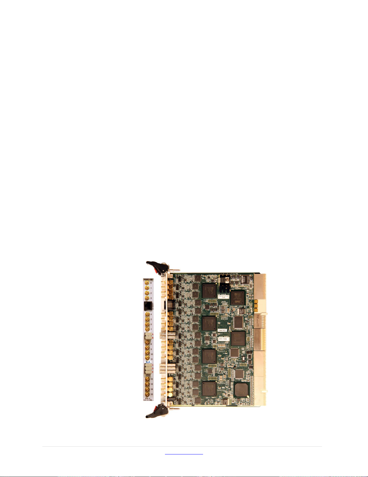
Figure 1-1: Picture of the front and side view of the Pixie-16.
Version 3.00 www.xia.com 8
Page 9

Pixie-16 User Manual August 21, 2018
1.1 Pixie-16 Features
Designed for
o Segmented germanium detectors,
o Silicon strip detectors,
o Arrays of scintillation detectors,
o Synchronous waveform capture for gamma- ray tracking,
o Sub-nanosecond timing measurements,
o Mixed systems with different detector types.
Accepts input signals directly from detector preamplifier outputs or scintillator/PMT
or SiPM combinations
12, 14, 16 bits; 100, 250, 500 MSPS ADC
Two software selectable gain/attenuation settings for each analog input
Programmable DC-offset for each analog input
Onboard CFD trigger with adjustable parameters
Programmable pileup inspection criteria include trigger filter parameters, threshold,
and rejection criteria
Triggered synchronous acquisition across channels and modules of waveforms up to
163 µs in length
On-board MCA spectrum from 1K to 32K bins (software selectable), up to 4.3
billion counts per bin
Event processing and optional pulse shape analysis performed with 100 MHz, 32-bit
floating point SHARC® DSP
Event by event list mode data buffered to allow zero dead-time acquisition
Full speed 32-bit, 33 MHz PCI interface to host computer, up to 109 MBytes/s
readout sustained
Configurable digital inputs and outputs
More than 120 backplane lines for clock and trigger distribution or general purpose
I/O and run synchronization between modules
Graphical user interfaces to control and diagnose system
Digital oscilloscope for health-of-system analysis
Compact C driver libraries available for easy integration in existing user interface
Version 3.00 www.xia.com 9
Page 10

Pixie-16 User Manual August 21, 2018
Front Panel I/O
Signal Input
16 analog signal inputs (SMB). Switchable input impedance and
attenuation: 50 Ω or 1 kΩ or 4 kΩ (or according to user specification), 1:4
or 1:1 attenuation
Jumper selectable 50 Ω input termination
Sixteen preamplifier inputs, switchable input impedance and attenuation:
50 Ω or 1 kΩ or 4 kΩ (or according to user specification)
Input signal is not recommended to exceed +/-3.5V if 50 Ohm input
termination jumper is installed and the 1:4 attenuation is not used
Works with common resistive feedback preamplifiers of either signal
polarity
Logic Input/output
28 digital inputs/outputs, including:
4 high speed LVDS input/output connections
16 LVDS inputs for channel specific veto (or validation)
2 LVDS inputs for module veto (or validation) or general purpose I/O
6 single-ended inputs and 6 single-ended outputs
Option for external clock through front panel input. In addition, there are
more than 120 digital lines on the backplane for low skew system clock
distribution, trigger, run synchronization, and global veto lines, and
complex trigger logic, multiplicity information, or data transfers between
modules
Backplane I/O
Clock Input/output
Distributed 50 MHz clock, dedicated PXI_CLK line from slot 2 or daisychained
Synchronization
Wired-or SYNC signal distributed through PXI backplane to synchronize
timers and run start/stop
Veto
VETO signal distributed through PXI backplane to suppress event
triggering
General purpose
I/O
More than 120 (121 for Rev F modules, 164 for Rev B/C/D modules)
bussed and neighboring lines on custom backplane to distribute
multiplicity and triggers and for I/O between modules
Data Interface
PCI
32-bit, 33MHz Read/Write, external memory or FIFO readout rate to host
over 100 MByte/s
Digital Controls
Input
Choice of two attenuation options through software settable input relay
Gain
Fixed analog voltage gain set to factory standard or per user specification,
digital gain adjustment possible
Offset
DC offset adjustment from –1.5V to +1.5V, in 65536 steps
1.2 Specifications
Table 1-1 Detailed Specifications of Pixie-16
Version 3.00 www.xia.com 10
Page 11

Pixie-16 User Manual August 21, 2018
Shaping (Slow
Filter)
Digital trapezoidal filter with adjustable rise time and flat top for pulse
height computation
Rise time and flat top: 0.04 to 80 s (0.032 to 65.5 s for 250 MHz
modules), set independently
Adjustable flat top to eliminate ballistic deficit effects
Trigger (Fast
Filter)
Digital trapezoidal filter with adjustable rise time, flat top and threshold
for pulse trigger detection
Rise time and flat top: 0.02 to 1.27 s (0.016 to 1.016 s for 250 MHz
modules), set independently
9-bit threshold values corresponding to 0 to 511 ADC steps
Constant Fraction
Discriminator
(CFD) trigger
Programmable CFD length, delay and scaling factor
Coincidence or
Multiplicity
Programmable coincidence pattern, coincidence window length, fast
trigger delays
Programmable multiplicity group pattern, multiplicity threshold
Data collection
MCA binning factor and number of bins
Waveform length and pre-trigger delay
Data Outputs
MCA spectrum
32,768 bins, 32 bit deep (4.2 billion counts/bin) for each channel
List mode event
data
256K16bit FIFO memory for buffering list mode data which consist of
event ID, time stamp (48-bit), CFD time (16-bit), energy (16-bit), and
optional waveform, raw energy sums, baseline, and QDC sums
Events are time stamped with 100 or 125 MHz clock with fractional CFD
time that is captured at full ADC clock rate (100 or 250 or 500 MHz)
Statistics
Real time, live time, input and output counts for each channel
Diagnostics
ADC trace, baseline history, baseline distribution, FFT noise spectrum
1.3 System Requirements
The digital spectroscopy system considered here consists of a host computer, one or more
Pixie-16 modules in a Pixie-16 crate, and a gamma ray detector with appropriate power
supplies.
1.3.1 Pixie-16 Crate
The Pixie-16 can be operated in any slot from 2 to 14 of a Pixie-16 crate. Slot 1 is used by
the crate controller.
1.3.2 Host Computer
The Pixie-16 module communicates with a host computer through a PCI interface. The
host computer is usually either an embedded PC installed in slot 1 of the Pixie-16 crate or
a remote desktop or laptop that is linked to the crate via a PCI bridge that is also installed
in slot 1.
The host computer must have the following minimum capabilities
~100 MB of disk space for operation software
Sufficient disk space for acquired data
Version 3.00 www.xia.com 11
Page 12

Pixie-16 User Manual August 21, 2018
Windows 7/10 (32 bit or 64 bit) (currently still compatible with Windows XP).
Operation under Linux is supported, please contact XIA for details.
There are no minimum processor requirements, but a clock rate of 1 GHz or more
and memory of 512 MB or more are recommended.
1.3.3 Drivers and Software
Communication between the Pixie-16 module and the host PC is facilitated by the PCI
driver files and API functions provided by PLX Technology (version 7.10). Drivers are
provided by the XIA software distribution. Standalone PLX PCI library files can be
downloaded from XIA’s web site. Please contact XIA for details.
The Pixie-16 software is a Windows based user interface for the Pixie-16 modules.
Alternative interfaces are ROOT (under Linux) or command line C programs; demo code
is provided on request.
1.3.4 Detector Signals
The Pixie-16 is designed for single exponentially decaying signals. Step pulses or short
non-exponential pulses can be accommodated with specific parameter settings. Staircase
type signals from reset preamplifiers generally need to be AC coupled.
The amplitude of the detector output signals is not recommended to exceed +/-3.5V if 50
Ohm input termination jumper is installed and the 1:4 attenuation is not used.
1.3.5 Power Requirements
The Pixie-16 consumes roughly between 40W and 50W (depending on ADC variants of
100 MHz to 500 MHz), requiring the following currents from the Pixie-16 crate:
1.8V 3 - 4 A
3.3V 3 - 4 A
5V5 3 - 4 A
-6V 1.5 A
1.3.6 Connectors and Cabling
The Pixie-16 uses SMB connectors for the analog inputs from the detectors. SMB to BNC
adapter cables are provided with the module.
A 10pin har-link® connector is used for digital inputs and outputs. The pin pitch is 2mm.
Matching cables are e.g. Harting 33 27 243 1000 002.
1.4 Software and Firmware Overview
For installation of the software and an introduction to the user interface, please refer to the
following chapter of this manual. For details on the driver layer, please refer to the
programmer’s manual.
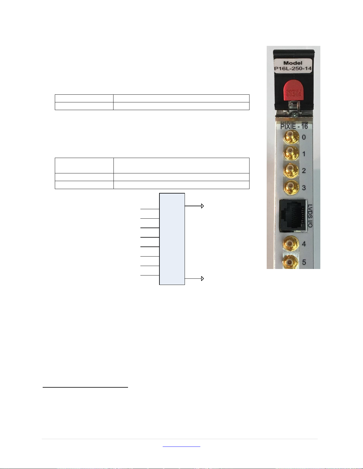
1.5 Front Panel
On the front panel of each Pixie-16 module, there are 16 analog signal input connectors,
one LVDS I/O port, five digital I/O connectors as well as three LEDs near the bottom of
the front panel. In addition, a sticker showing Pixie-16 model number (e.g., P16L-250-14,
meaning the 14-bit, 250 MHz variant of the Pixie-16) is affixed to the top handle of the
Version 3.00 www.xia.com 12
Page 13
Pixie-16 User Manual August 21, 2018
Connector Labels
0 to 15 for 16 channels
Connector Type
SMB Jack
Connected Signals
4 LVDS pairs (Fo1p/Fo1n, Fi1p/Fi1n, Fi5p/Fi5n,
Fo5p/Fo5n, see below for pin layout)
Signal Direction
Input or Output, software configurable
Cable Type
Cat 5 or Cat 6 (the same ones used for Ethernet)
J101
5
4
3
2
1
6
7
8
10
9
Fo
1p
Fo
1n
Fi
1p
Fi
1n
Fi
5p
Fi
5n
Fo
5p
Fo
5n
1
front panel, and another sticker indicating the serial number of the
Pixie-16 module (e.g., S/N 1100) is placed at the bottom handle of
the front panel.
1.5.1 16 Analog Signal Input Connectors (all Pixie-16 revisions1)
Table 1-2 Pixie-16 Analog Signal Input Connectors
Each Pixie-16 module accepts 16 analog input signals, and each
input connector is a SMB Jack (male contact) connector.
1.5.2 LVDS I/O Port (all Pixie-16 revisions)
Table 1-3 Pixie-16 LVDS I/O Port
Each Pixie-16 module is equipped with one LVDS I/O port on its front panel. LVDS stands
for low voltage differential signaling. The LVDS I/O connector is a RJ45 connector, which
implies that the same Cat 5 or Cat 6 Ethernet cables can be used to connect signals to or
from this I/O port. However, no Ethernet connectivity is available through this Pixie-16
I/O port.
Four differential signal pairs, i.e., between pin-pairs Fo1p/Fo1n, Fi1p/Fi1n, Fi5p/Fi5n, and
Fo5p/Fo5n, are available from this I/O port. Each pair can be configured as either an input
or output signal.
The most frequent use of this LVDS I/O port is accepting veto signals in Compton
Revision for a given Pixie-16 module can be determined based on its serial number: S/N 120-134 -> Rev. B; S/N
135-199 -> Rev. C; S/N 200-274 -> Rev. D; S/N 1000 and up -> Rev. F
Version 3.00 www.xia.com 13
suppressed Clover detector systems. In such systems, each Clover detector has four
Figure 1-2: Pixie-16 LVDS I/O Port.
Page 14
Pixie-16 User Manual August 21, 2018
G0_P FI4
B
A2
FI3
B2 C2 D2 E2
A1 B1 C1 D1 E1
G0_N
G1_P G2_P G3_P
G1_N
G2_N G3_N
G7_P FI0
C
A2
FI2
B2 C2 D2 E2
A1 B1 C1 D1 E1
G7_N
G6_P G4_P G5_P
G6_N
G4_N G5_N
G9_P MG_P
D
A2
MG_N
B2 C2 D2 E2
A1 B1 C1 D1 E1
G9_N
G8_P G10_P G11_P
G8_N
G10_N G11_N
G14_P SG_P
E
A2
SG_N
B2 C2 D2 E2
A1 B1 C1 D1 E1
G14_N
G12_P G15_P G13_P
G12_N
G15_N G13_N
FO0 FI6
A
A2
FI7
B2 C2 D2 E2
A1 B1 C1 D1 E1
FO2 FO4
FO3
FO6 FO7
individual HPGe crystals which are surrounded by an anti-Compton shield (e.g., BGO
crystal + PMT readout). If the veto signals from the anti-Compton shield are generated
using external electronics and then converted to LVDS format (e.g., using XIA’s LVDS
fanout boards), 4 such veto signals can then be input to one Pixie-16 module using the
LVDS I/O port. In this way, 4 Compton suppressed Clover detectors (16 HPGe crystal
outputs to 16 input channels of the Pixie-16) can be instrumented by one Pixie-16 module.
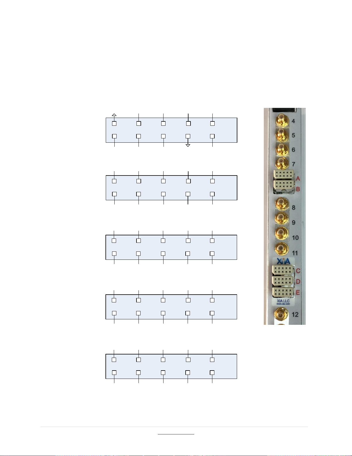
1.5.3 Digital I/O Connectors (A, B, C, D, E in red color font) (Rev. F Modules only)
Figure 1-3: Pixie-16 Digital I/O Connectors A, B, C, D and E.
Version 3.00 www.xia.com 14
Page 15

Pixie-16 User Manual August 21, 2018
Connector Type
har-link (HARTING, 2mm pin spacing)
FI0, FI2, FI3, FI4, FI6, FI7
TTL digital input signals (max. 5V)
FO0, FO2, FO3, FO4, FO6, FO7
Digital outputs for test/debug purpose (TTL 5V)
Gx_P/Gx_N (x=0-15)
Channel Gate Inputs (0-15 for 16 channels) (LVDS format)
MG_P/MG_N
Module Gate Input (LVDS format)
SG_P/SG_N
Spare Gate Input (LVDS format)
Table 1-4 Pixie-16 Rev. F Module’s Digital I/O Connectors
The Pixie-16 Rev. F modules are equipped with five har-link connectors on its front panel
which act as digital I/O connectors. The 2mm pitch har-link connector from HARTING
is designed for high speed data transfer with rates up to 2 Gbit/s. Its EMI shielding, shown
in Figure 1-4, guarantees excellent performance in EM-polluted environment.
Figure 1-4: 2mm pitch har-link connector from HARTING.
Each har-link connector has 2 rows with 5 pins on each row, and is labelled using one of
the five letters in red color font, from A to E. The signals connected to each pin of these
five connectors are shown in Table 1-4. Among them, FI0, FI2, FI3, FI4, FI6, FI7 are six TTL
digital input signals. They can be signals like global fast trigger, global validation trigger,
external clock, run inhibit, etc. The specific usage of each input pin is determined by the
specific firmware that is downloaded to the Pixie-16 module (see Table 1-9 for input
signals supported by the standard firmware). The six digital output signals, FO0, FO2, FO3,
FO4, FO6, FO7, which are connected to six test output pins on the System FPGA of the
Pixie-16, can be used to assist a user in the process of system setup. These test pins are
connected to various internal signals of the Pixie-16 to provide insight of the current status
of the system.
The Channel Gate Inputs (0-15 for 16 channels) are LVDS format input signals which
independently gate the data acquisition of each of the 16 channels of a Pixie-16 module.
The Channel Gate signal is level sensitive signal, i.e., when the level of the Channel Gate
Signal is logic high (1), the gate signal is effective; when the level of the Channel Gate
Signal is logic low (0), the gate signal is not in use. In normal cases, the Channel Gate
Signal is set up to veto the data acquisition in a given channel, i.e., at the time of the arrival
of fast trigger in that channel, if the Channel Gate Signal is logic high (1), that fast trigger
is discarded since it is vetoed. However, this type of logic can be reversed through setting
corresponding registers in the FPGA via software. In such cases, the Channel Gate Signal
is set up to validate the data acquisition in a given channel, i.e., at the time of fast trigger
in that channel, only if the Channel Gate Signal is logic high (1) will that fast trigger be
accepted to have the event recorded.
Version 3.00 www.xia.com 15
Page 16
Pixie-16 User Manual August 21, 2018
LED Name
Color
Function
RUN
Green
ON when run is in progress, and OFF if run is
stopped or not started yet
I/O
Yellow
Flashing when there is I/O activity on the PCI
bus between the Pixie-16 module and host
computer
ERR
Red
ON when there is no more space in the External
FIFO for storage of list mode event data, and
OFF when there is sufficient space to store at
least one more list mode event data
(ON does not indicate any actual error
condition. Rather, it simply indicates the
External FIFO’s FULL condition)
The Module Gate Input is a LVDS format signal that gates the data acquisition in all 16
channels of a Pixie-16 module. It is also a level sensitive signal, i.e., when the level of the
Module Gate Signal is logic high (1), the gate signal is effective; when the level of the
Module Gate Signal is logic low (0), the gate signal is not in use. In normal cases, the
Module Gate Signal is set up to veto the data acquisition in all 16 channels, i.e., at the time
of the arrival of fast trigger in any of the 16 channels, if the Module Gate Signal is logic
high (1), that fast trigger of that channel is discarded since it is vetoed. However, this type
of logic can be reversed through setting corresponding registers in the FPGA via software.
In such cases, the Module Gate Signal is set up to validate the data acquisition in all 16
channels, i.e., at the time of fast trigger in any of the 16 channel, only if the Module Gate
Signal is logic high (1) will that fast trigger of that channel be accepted to have the event
recorded.
The Spare Gate Input is a LVDS format signal that is reserved for special applications.
Such applications typically require development of custom firmware to support special
functionalities of the Pixie-16 system.
1.5.4 Front Panel LEDs (all Pixie-16 revisions)
Table 1-5 Front Panel LEDs for the Pixie-16 Modules
Near the bottom of the Pixie-16 front panel, there are three LEDs. They
are labelled as RUN, I/O, and ERR, respectively, from left to right. They
correspond to three different colors, green, yellow, and red,
respectively.
The RUN LED will be turned on when a run in the Pixie-16 module is
in progress, and will be turned off when the run is stopped or not started
yet. The I/O LED will blink when there is I/O activity on the PCI bus
between the Pixie-16 module and host computer. The ERR LED is, in fact, not to signal
any error condition in the Pixie-16 module. Instead, it is used to indicate whether or not the
External FIFO of the Pixie-16 module is full. It will be ON when there is no more space in
the External FIFO for storage of list mode event data, and OFF when there is sufficient
space to store at least one more list mode event data. When the External FIFO is full, no
more list mode event data can be written into it until the host software reads out part of the
Version 3.00 www.xia.com 16
data in the External FIFO through the PCI bus.
Page 17
Pixie-16 User Manual August 21, 2018
Connector Type
Single-ended, 2mm pin spacing
FO0, FO2, FO3, FO4,
FO6, FO7
Digital outputs for test/debug
purpose (3.3V)
J200
10
8
6
4
2 1
3
5
7
9
Fo
0
Fo
2
Fo
4
Fo
3
Fo
6
Fo
7
Connector Type
Amphenol FCI 55 Position Header, 2mm pin
spacing
FI0, FI2, FI3, FI4, FI6, FI7
TTL digital input signals (max. 5V)
Gxin+/Gxin- (x=0-15)
Channel Gate Inputs (0-15 for 16 channels)
(LVDS format)
MGin+/MGin-
Module Gate Input (LVDS format)
SGin+/SGin-
Spare Gate Input (LVDS format)
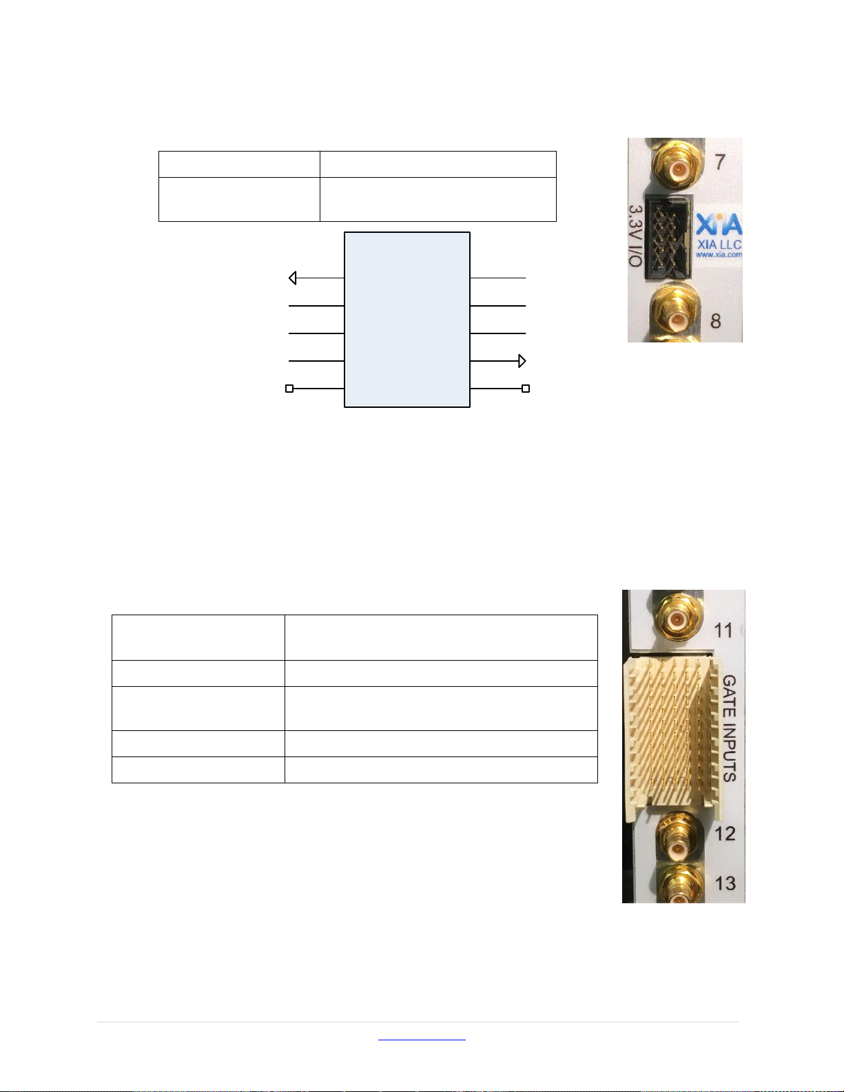
1.5.5 3.3V I/O Connector (Rev. D Modules only)
Table 1-6 Pixie-16 Rev. D Module’s 3.3V I/O Connector
Figure 1-5: Pixie-16 Rev. D Module’s 3.3V I/O Connector.
On Rev. D Pixie-16 modules, between analog input SMB connectors for channel 7 and
channel 8, respectively, is the 3.3V I/O Connector (J200). It has 10 single-ended pins with
2mm spacing. Pins #1, 3, 4, 5, 6, and 8 are connected to six digital output signals from the
System FPGA of the Pixie-16 module, i.e. FO0, FO2, FO3, FO4, FO6, FO7, mainly for the
purpose of testing and debugging. Pins #2 and 7 are ground pins, and pins #9 and 10 are
not in use.
1.5.6 GATE Inputs (Rev. D Modules only)
Table 1-7 Pixie-16 Rev. D Module’s GATE Inputs
On Rev. D Pixie-16 modules, between analog input SMB connectors
for channel 11 and channel 12, respectively, is the GATE INPUTS
connector. This connector is an Amphenol FCI 55 Position Header
with 2mm pin spacing. The layout of these 55 pins is shown in Figure
1-6. The 11 pins from the middle pin column (J150C) are all tied to
the Ground. Among the first 8 rows of the GATE INPUTS
connector, each differential pair of pins from the A/B columns
Version 3.00 www.xia.com 17
(J150A/J150B) or the D/E columns (J150D/J150E) corresponds to one channel’s GATE
INPUT, which has the LVDS format, e.g. Gxin+/Gxin- (x=0-15). Differential pair of pins at
J150A3/J150B3 is the Module Gate Input signal, MGin+/MGin-. Channel Gate Input signal
can be used to veto or validate that given channel’s own trigger. Module Gate Input signal
Page 18
Pixie-16 User Manual August 21, 2018
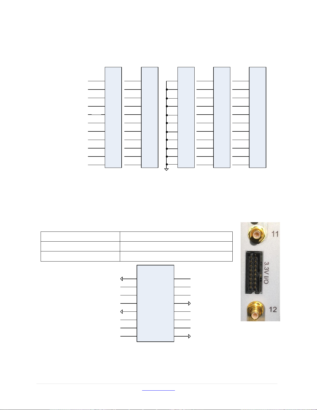
J150A
A1
A5
A4
A3
A2
A6
A7
A8
A9
A10
A11
Fi6
Fi0
MGin+
G14in +
G12in +
G10in +
G8in+
G6in+
G4in+
G2in+
G0in+
J150B
B1
B5
B4
B3
B2
B6
B7
B8
B9
B10
B11
Fi7
Fi2
MGin-
G14in-
G12in-
G10in-
G8in-
G6in-
G4in-
G2in-
G0in-
J150C
C1
C5
C4
C3
C2
C6
C7
C8
C9
C10
C11
J150D
D1
D5
D4
D3
D2
D6
D7
D8
D9
D10
D11
Fi3
SGin+
G15in+
G13in+
G11in+
G9in+
G7in+
G5in+
G3in+
G1in+
J150E
E1
E5
E4
E3
E2
E6
E7
E8
E9
E10
E11
Fi4
SGin-
G15in-
G13in-
G11in-
G9in-
G7in-
G5in-
G3in-
G1in-
Connector Type
Single-ended, 2mm pin spacing
FI0, FI2, FI3, FI4, FI6, FI7
TTL digital input signals (max. 5V)
FO0, FO2, FO3, FO4, FO6, FO7
Digital outputs for test/debug purpose (3.3V)
J100
10
8
6
4
2 1
3
5
7
9
12 11
14 13
16 15
Fo
3
Fo
6
Fo
7
Fo
0
Fo
2
Fo
4
Fi
0
Fi
2
Fi
4
Fi
3
Fi
6
Fi
7
works on the whole module level, i.e. it can be used to veto or validate all 16 channels’
own trigger of that given module. Differential pair of pins at J150D3/J150E3 is the Spare
Gate Input signal, SGin+/SGin-. Spare Gate Input signal can be used for special applications
which require a custom firmware.
Figure 1-6: Pixie-16 Rev. D Module’s GATE INPUTS Connector.
On Rev. D Pixie-16 modules, the TTL digital input signals (max. 5V), i.e. FI0, FI2, FI3, FI4,
FI6, FI7, are distributed among the bottom two rows of the GATE INPUTS Connector, as
illustrated in Figure 1-6.
1.5.7 3.3V I/O Connector (Rev. B and C Modules only)
Table 1-8 Pixie-16 Rev. B and C Module’s 3.3V I/O Connector
Version 3.00 www.xia.com 18
On Rev. B and C Pixie-16 modules, between analog input SMB connectors for channel 11
and channel 12, respectively, is the 3.3V I/O Connector (J100). It has 16 single-ended pins
Figure 1-7: Pixie-16 Rev. B and C Module’s 3.3V I/O Connector.
Page 19

Pixie-16 User Manual August 21, 2018
TTL digital
input signals
Connected signals in
standard firmware
Direction
Description
FI0
EXT_FASTTRIG
Input
External fast trigger signal
FI2
INHIBIT
Input
Run inhibit signal
FI3
EXT_TS_CLK
Input
External timestamp clock signal
FI4
EXT_VALIDTRIG
Input
External validation signal
FI6
not used
FI7
EXT_TS_CLR
Input
External timestamp clear signal
with 2mm spacing. Pins #1, 3, 4, 5, 6, and 8 are connected to six digital output signals from
the System FPGA of the Pixie-16 module, i.e. FO0, FO2, FO3, FO4, FO6, FO7, mainly for
the purpose of testing and debugging. Pins #2, 7, 10 and 15 are ground pins. Pins #9, 11,
12, 13, 14 and 16 are connected to the six TTL digital input signals (max. 5V), i.e. FI0, FI2,
FI3, FI4, FI6, FI7.
1.5.8 Digital Input/output Signals Supported by Standard Firmware (all Pixie-16
revisions)
The standard firmware of the Pixie-16 supports input and output of digital signals through
its front panel I/O connectors, which were discussed earlier.
Table 1-9 shows the five TTL digital input signals supported by the Pixie-16 standard
firmware. Among them, the signals EXT_TS_CLK and EXT_TS_CLR are used for
external timestamping in the Pixie-16, i.e. the Pixie-16 accepting an external clock signal
(the frequency of this external clock is not recommended to exceed about 20 MHz in order
to avoid the clock signal integrity issue), counting such clock signal with a 48-bit counter,
and outputting such counter value to the list mode data stream when an event trigger occurs.
The external timestamping is useful for synchronizing the Pixie-16 data acquisition system
with another data acquisition system through correlating the external timestamps of the
events recorded by both systems.
The INHIBIT signal is used by an external system to inhibit the data acquisition run in a
Pixie-16 system when synchronization requirement is enabled in the Pixie-16 modules. It
is a level sensitive signal, i.e. when the INHIBIT signal is at the logic high level, the run in
the Pixie-16 won’t start. Only when the INHIBIT signal goes to the logic low level will the
run start in the Pixie-16. During the run, if the INHIBIT signal returns to the logic high
level, the run will be aborted.
The EXT_FASTTRIG signal is the external fast trigger signal, which can be used to replace
the local fast trigger for recording events in the Pixie-16 modules. The EXT_VALIDTRIG
signal is the external validation signal, which can be used to validate events in the Pixie16 modules.
Table 1-9 Pixie-16 TTL Digital Input Signals
Version 3.00 www.xia.com 19
Table 1-10 shows the Pixie-16 connector J101 LVDS I/O port signals. This J101 LVDS
I/O port can use the regular Ethernet cable for connection but it does not have Ethernet
connectivity. Among the four LVDS pairs available from this J101 port, one pair is
currently not in use, two pairs are used for input and one pair is used for output. The
LVDS_VALIDTRIG is the external validation trigger signal in LVDS format, and the
LVDS_FASTTRIG is the external fast trigger signal in LVDS format. The
Page 20

Pixie-16 User Manual August 21, 2018
Connector
J101 Pins
Connected signals in
standard firmware
Direction
Description
Fo1p/Fo1n
not used
Fi1p/Fi1n
LVDS_VALIDTRIG
Input
External validation trigger signal in
LVDS format
Fi5p/Fi5n
LVDS_FASTTRIG
Input
External fast trigger signal in LVDS
format
Fo5p/Fo5n
SYNC_LVDS_FP
Output
Pixie-16 synchronization output signal
in LVDS format (to synchronize with
other DAQ systems)
TTL digital
output
signals
Connected signals in standard
firmware
Direction
Description
FO0
FTRIG_DELAY
FTRIG_DELAY
Output
Delayed local fast
trigger of one of
the 16 channels
Delayed local fast
trigger of one of
the 16 channels
FO2
FTRIG_VAL
VETO_CE
Output
Validated,
delayed local fast
trigger one of the
16 channels
Stretched veto
trigger of one of
the 16 channels
FO3
ETRIG_CE
LDPMFULL
Output
Stretched external
global validation
trigger of one of
the 16 channels
Module level dual
port memory
(DPM) full status
flag
FO4
CHANTRIG_CE
SDPMFULL
Output
Stretched channel
validation trigger
of one of the 16
channels
System level dual
port memory
(DPM) full status
flag
FO6
FTIN_OR
FTIN_OR
Output
OR of 16 local
fast triggers
OR of 16 local
fast triggers
FO7
TEST_SEL
TEST_SEL
Output
Selected test
signal
Selected test
signal
SYNC_LVDS_FP is an output signal from the Pixie-16 module to indicate to external data
acquisition systems the synchronization status of the Pixie-16 system so that both data
acquisition systems can be synchronized.
Table 1-10 Pixie-16 Connector J101 LVDS I/O Port Signals
Table 1-11 Pixie-16 TTL Digital Output Signals
Table 1-11 lists the six Pixie-16 TTL digital output signals. Two groups of six output
signals can be chosen through software settings (see Table 3-9, bits [14:12] and [19:16] of
TrigConfig0). The last output signal TEST_SEL can be further selected through software
settings. More details about these signals will be provided in later sections of this manual.
Version 3.00 www.xia.com 20
Page 21
Pixie-16 User Manual August 21, 2018
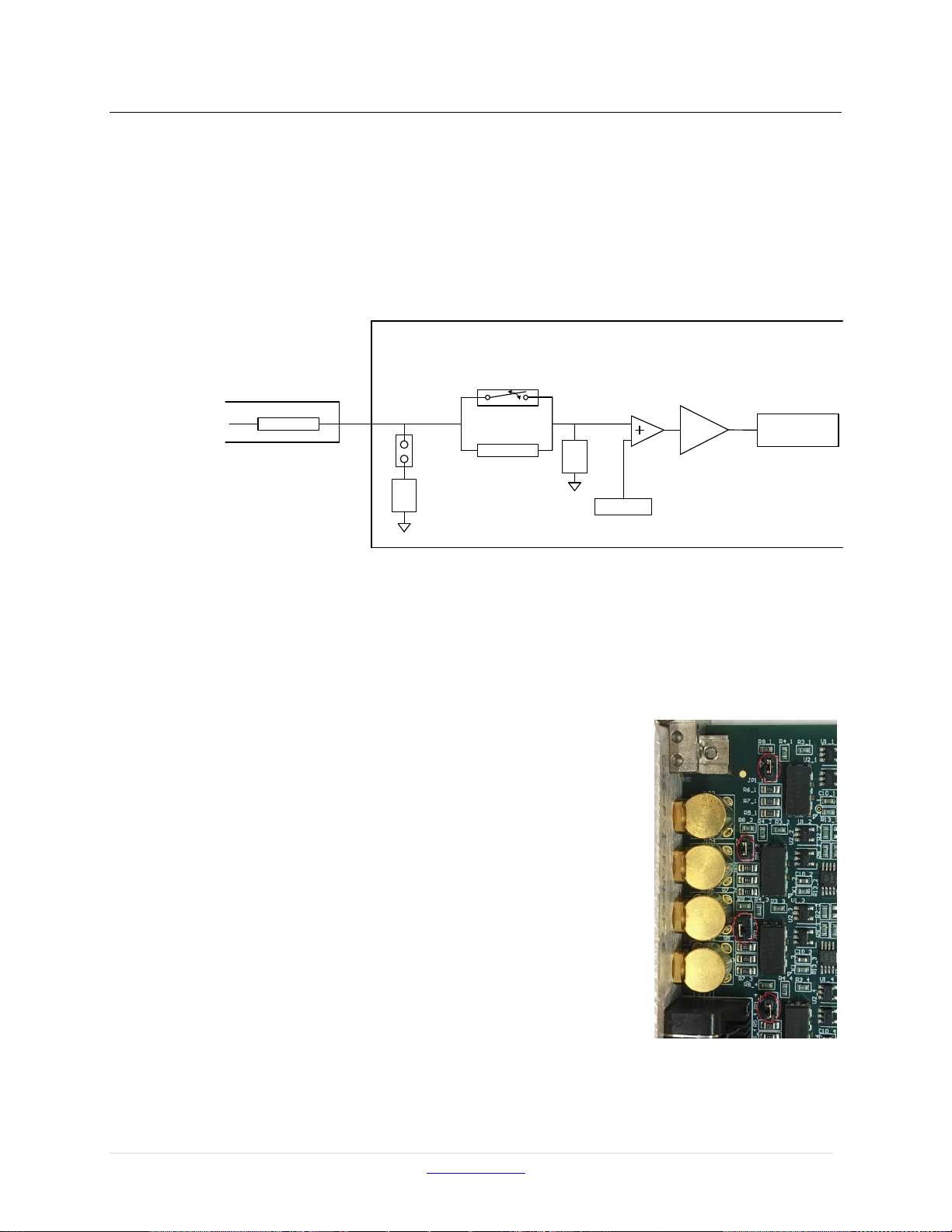
Detector Preamp
50 W
Pixie-16 Rev. F
Illustration of one channel’s analog input stages
50
W
Jumper
JP1_x
x=1...16
3k W
Relay Switch (software controllable)
1k
W
Offset DAC
Gain
(x2.5)
ADC
(Max Vp-p = 2V)
If Jumper is not installed:
If Relay Switch is closed, attenuation is 1:1 (1k W termination), and overall effective gain is 2.5;
If Relay Switch is opened, attenuation is 1:4 (4k W termination), and overall effective gain is 0.625;
If Jumper is installed and detector preamplifier has 50 W output impedance:
If Relay Switch is closed, attenuation is 1:1 (47.6 W termination), and overall effective gain is 1.25;
If Relay Switch is opened, attenuation is 1:4 (49.4 W termination), and overall effective gain is 0.3125.
[-1.5V...+1.5V]
1.6 Front End Attenuation and Termination
Each Pixie-16 module has 16 independent analog input channels. To ensure analog input
signal can be properly digitized by each channel’s ADC, the signal must undergo proper
signal conditioning including 1) adjusting DC offset of the analog input signal using each
channel’s independent Offset DAC and 2) selecting proper input attenuation. The goal of
the analog signal conditioning is to fit the analog input signal into the ADC input voltage
range (2Vpp).
1.6.1 Rev. F Modules
The input stages of the Rev. F Pixie-16 modules are shown in
Figure 1-8. Each channel’s input termination jumper (JP1_x,
x=1…16), shown on the right in red circles, is used to connect
the analog input signal to a 50 W resistor then to ground. It is
installed by default at the factory, and is recommended for
being used to avoid input signal reflection when using long
coaxial cables to connect detector outputs to the Pixie-16
front panel connectors. However, if the detector outputs have
50 W output impedance, the signal will be effectively halved
at the input of the Pixie-16 when the input termination jumper
is installed.
A relay switch, which is controlled by software for closing or
opening, can be used to choose between two attenuation
factors and thus two overall effective gains for each of the 16
Pixie-16 input channels. The notes section of Figure 1-9
describes the effective attenuation factor, input impedance,
and overall gain for the four cases of the combinations of jumper installation and relay
switch. If different overall effective gains than the ones provided by the factory standard
(i.e. 2.5/0.625 or 1.25/0.3125) are necessary, please contact XIA for possible custom input
Figure 1-8: Rev. F Pixie-16 input stages.
Version 3.00 www.xia.com 21
Page 22
Pixie-16 User Manual August 21, 2018
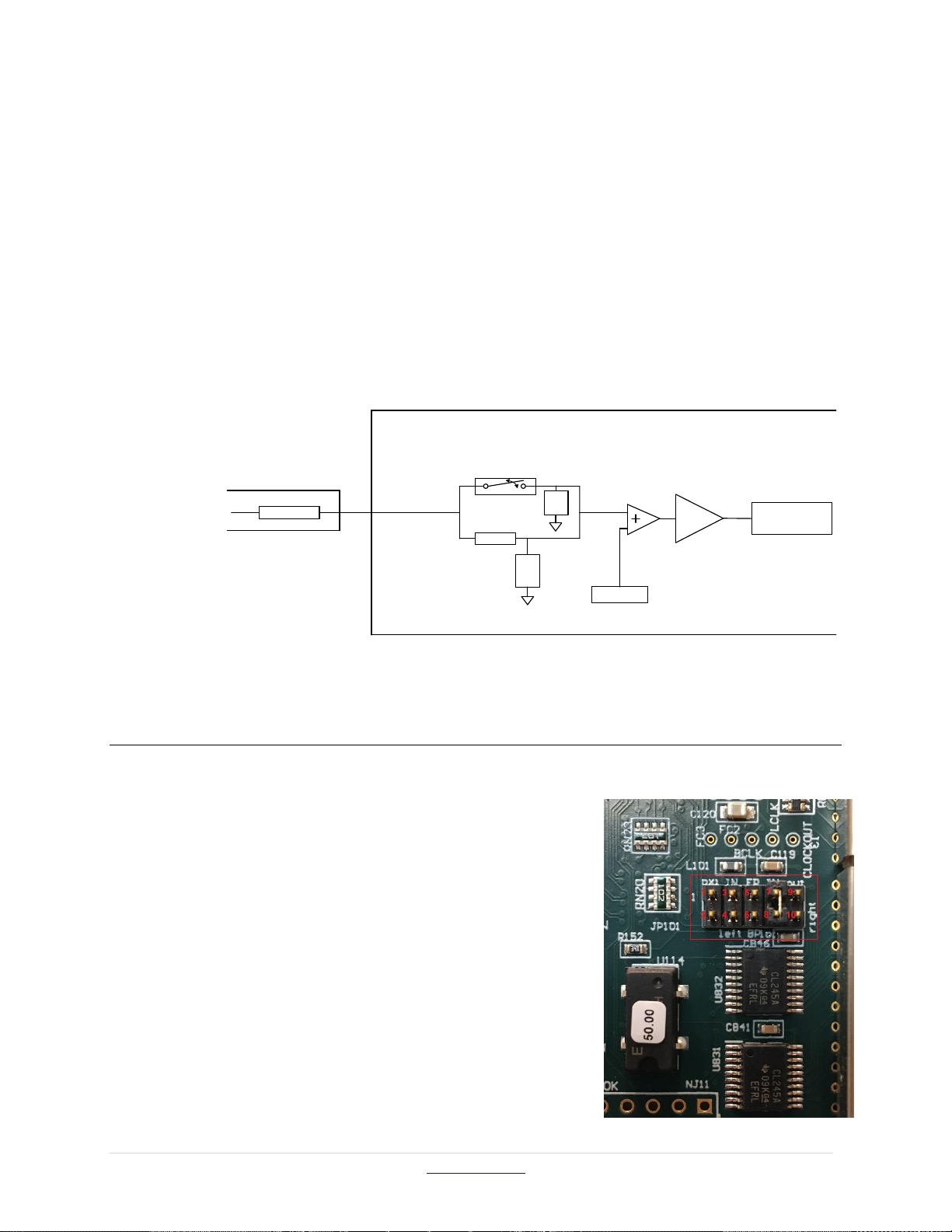
Detector Preamp
50 W
Pixie-16 Rev. B,C,D
Illustration of one channel’s analog input stages
820 W
Relay Switch (software controllable)
240
W
Offset DAC
Gain
(x4)
ADC
(Max Vp-p = 2V)
If detector preamplifier has 50 W output impedance:
If Relay Switch is closed, attenuation is 1:1 (50 W termination), and overall effective gain is 2;
If Relay Switch is opened, attenuation is 1:4 (1k W termination), and overall effective gain is 0.9.
[-1.5V...+1.5V]
50
W
gains. That most likely will involve changing certain parts of the Pixie-16 input stages.
Other options will be either to change the gain of the detector preamplifier (if feasible) or
to change the high voltage supplied to the detectors (e.g. PMT or SiPM, etc.).
1.6.2 Rev. B, C, D Modules
Different from their Rev. F counterparts, Rev. B, C, D modules do not have the input
termination jumpers, and the input signal attenuation factors are also slightly different.
Figure 1-9 illustrates the input stages of the Rev. B, C, D Pixie-16 modules. Same as the
Rev. F modules, they also have a software controlled relay switch. When the relay switch
is closed, the input signal is tied to ground via a 50 W resistor, which effectively halves the
input signal if it has a 50 W output impedance. If the relay switch is opened, the input signal
passes through a second branch, which results in a 1:4 attenuation with a 1k W input
termination. The overall effective gain is 2 or 0.9 when the relay switch is closed or opened,
respectively.
Figure 1-9: Rev. B, C, D Pixie-16 input stages.
1.7 Operating Multiple Pixie-16 Modules Synchronously
When many Pixie-16 modules are operated together
as a system, it may be required to synchronize clocks
and timers between them and to distribute triggers
across modules. It will also be necessary to ensure that
runs are started and stopped synchronously in all
modules. All these signals are distributed through the
PXI backplane of the Pixie-16 crate.
1.7.1 Clock Distribution
In a multi-module system there will be one clock
master and a number of clock slaves or repeaters. The
clock function of a module can be selected by setting
shunts on Jumper JP101 near the bottom right corner
of the board. The 10-pin Jumper JP101 is shown in the
picture on the right with those pins labelled in red
color. Shunts are provided to connect pins that are
Version 3.00 www.xia.com 22
Page 23
Pixie-16 User Manual August 21, 2018
appropriate for each chosen clock distribution mode. Four clock distribution modes,
individual clock mode, PXI clock mode, daisy-chained clock mode, and multi- crate clock
mode, are described below.
Please note, in 250 MHz or 500 MHz Pixie-16 modules, the frequency of signal processing
clock in the FPGA has been divided down to either 125 MHz or 100 MHz, respectively,
for more practical implementation of the design. That division might result in different
clock phase and thus different timestamp offset for each channel within a given 250 MHz
or 500 MHz Pixie-16 module whenever the module is reinitialized. Calibration might be
needed to quantify the different timestamp offset for each channel.
1.7.1.1 Individual Clock Mode
If only one Pixie-16 module is used in the
system, or if clocks between modules do not
need to be synchronized, the module(s) should
be set into individual clock mode. Connect pin
7 of JP101 (the clock input) with a shunt to pin
8 (loc – IN). This will use the 50 MHz local
crystal oscillator of the Pixie-16 module as the
clock source.
Figure 1-10: Pixie-16 individual clock mode.
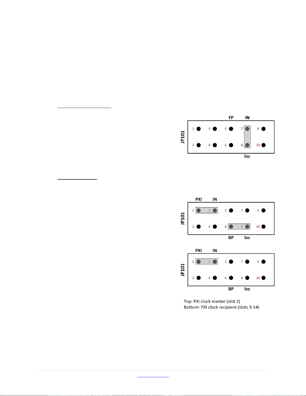
1.7.1.2 PXI Clock Mode
The preferred way to distribute clocks among multiple Pixie-16 modules is to use the PXI
clock distributed on the backplane. This clock
is by default generated on the backplane and is
a 10MHz clock signal, which is then repeated
by a fan out buffer and connected to each crate
slot by a dedicated line with minimum skew
(equal trace length to each slot). Although the
10MHz is too slow to be a useful clock for the
Pixie-16, it can be overridden by a local clock
signal from a Pixie-16 module that is installed
in slot 2 through proper shunt settings on the
JP101.
A Pixie-16 module can be configured to be the
PXI clock master in slot 2 by connecting pins
6 and 8 (loc – BP) of the JP101. All modules,
including the clock master, should be set to
receive the PXI clock by connecting pin 1 and
3 on JP101 (PXI – IN). In this way, the 50
MHz clock from the Pixie-16 clock master is
distributed to all Pixie-16 modules through the
backplane with nearly identical clock phase.
Figure 1-11: Pixie-16 PXI clock mode.
One other advantage of the PXI clock mode over the daisy-chained clock mode, which will
be discussed next, is that except for the Pixie-16 master module, which has to be installed
in slot 2, other Pixie-16 slave modules can be installed in any other slot of the Pixie-16
crate. In contrast, when the daisy-chained clock mode is used, all Pixie-16 modules have
to be installed next to each other, i.e. no gap is allowed between modules.
Version 3.00 www.xia.com 23
Page 24
Pixie-16 User Manual August 21, 2018
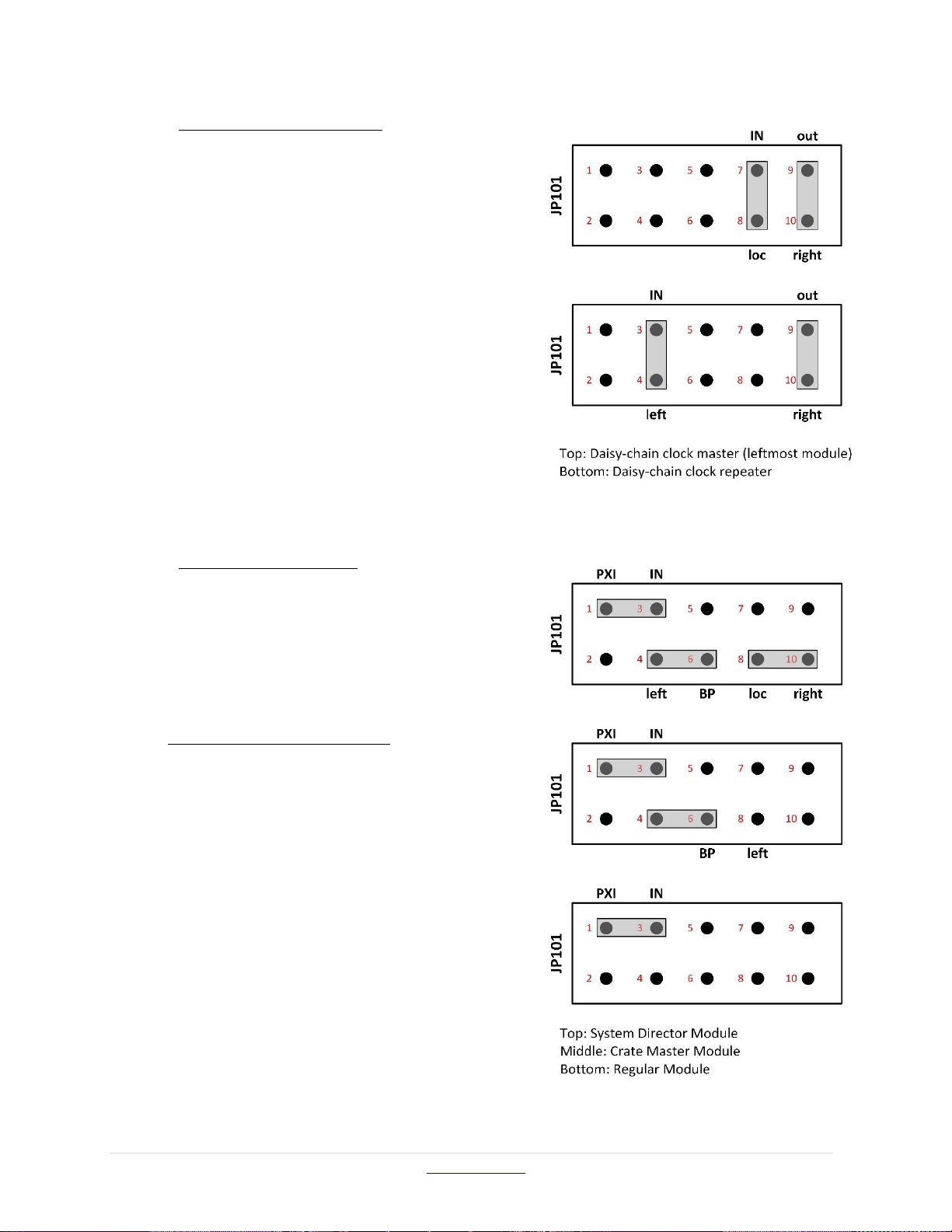
1.7.1.3 Daisy-chained Clock Mode
A further option for clock distribution is to
daisy-chain the clocks from one module to
the other, with each module repeating the
clock signal and transmitting it to the
neighbor on the right. This requires one
master module, located in the leftmost slot of
the group of Pixie-16 modules. The master
module uses its local crystal oscillator as the
input and sends its output to the right (loc –
IN, out – right). Other Pixie-16 modules in
the crate should be configured as clock
repeaters by using the signal from the left
neighbor as the input and sending its output
to the right (left – IN, out – right). However,
as mentioned earlier, there must be no slot
gap between modules.
Figure 1-12: Pixie-16 daisy-chained clock mode.
1.7.1.4 Multi-Crate Clock Mode
In multi- crate systems, a global clock signal
can be distributed among these crates using
dedicated trigger and clock distribution
cards, i.e. the Pixie-16 Rear I/O trigger
modules, which are available from XIA.
An example of clock distribution between
two crates is illustrated below.
Installation of Pixie-16 Modules
Multiple Pixie-16 modules can be installed
in two 14-slot Pixie-16 crates, #1 and #2. For
clock distribution purpose, crate #1 is called
the Master crate, where the system-wide
global clock for all Pixie-16 modules is
originated, and crate #2 is called the Slave
crate, which receives the global clock from
the Master crate.
The Pixie-16 module installed in slot 2 of the
Master crate is designated as the System
Director Module, whose local 50 MHz
crystal oscillator acts as the source of the
system-wide global clock. The distribution
of the clock signal from the System Director
Module to all Pixie-16 modules in the 2-crate
system is done through the Pixie-16 Rear I/O
trigger modules.
Figure 1-13: Pixie-16 multi-crate clock mode.
Version 3.00 www.xia.com 24
Page 25

Pixie-16 User Manual August 21, 2018
Crate #
1
Slot # 2 3 … 13
14
Module
System Director Module /
Crate Master Module
Regular
Module
…
Regular
Module
Regular
Module
Crate #
2
Slot # 2 3 … 13
14
Module
Crate Master Module
Regular
Module
…
Regular
Module
Regular
Module
System Director Module
Connect pins 1 and 3, 4 and 6, 8 and 10.
Crate Master Module
Connect pins 1 and 3, 4 and 6.
Regular Module
Connect pins 1 and 3.
The Pixie-16 module installed in slot 2 of the Slave crate is called the crate Master module,
which is responsible for receiving the global clock from the Master crate and sending such
clock to all modules in that crate through length-matched traces on the backplane. The
System Director Module is also responsible for sending the global clock to all modules in
the Master crate. Therefore, it is also a crate Master module. Other modules in these two
crates are regular modules. Table 1-12 shows the different types of modules in a 2-crate
system.
Table 1-12 Pixie-16 Module Definitions in a 2-crate System
Clock Jumper (JP101) Settings on the Pixie-16 Modules
For all Pixie-16 modules in a 2-crate system to use the same global clock signal, the clock
jumper (JP101) in all modules should be set according to Table 1-13 and Figure 1-13.
Table 1-13 Pixie-16 Clock Jumper JP101 Settings in a 2-crate System
Cable Connections for Pixie-16 Rear I/O Trigger Modules
The Pixie-16 Rear I/O trigger modules are
installed at the rear side of each crate where a
6U card cage is installed. Figure 1-14 shows
a Pixie-16 Rear I/O trigger module is
installed directly behind either the Director or
the Master module, respectively, to share
clock, triggers, and run start or stop
synchronization signals among multiple
Pixie-16 crates. The rear of the backplane has
connectors J3, J4 and J5, but it does not have
J1 and J2, since it does not need to use
CompactPCI or PXI communication.
Typically the first slot at the rear of the
backplane with J3, J4, J5 connectors installed
is the slot where the Pixie-16 Rear I/O trigger
module should be installed. While installing
the module, please ensure the alignment of
top and bottom rails with the trigger module
to avoid damage to the backplane pins.
Figure 1-14: Pixie-16 rear I/O trigger modules.
Version 3.00 www.xia.com 25
Page 26
Pixie-16 User Manual August 21, 2018
J200
J201
J202
J203
J204
J205
J206
J207
J209
J208
Trigger
board #1
installed in
the rear
slot #2 of
Crate #1
Trigger
board #2
installed in
the rear
slot #2 of
Crate #2
J200
J201
J202
J203
J204
J205
J206
J207
J209
J208
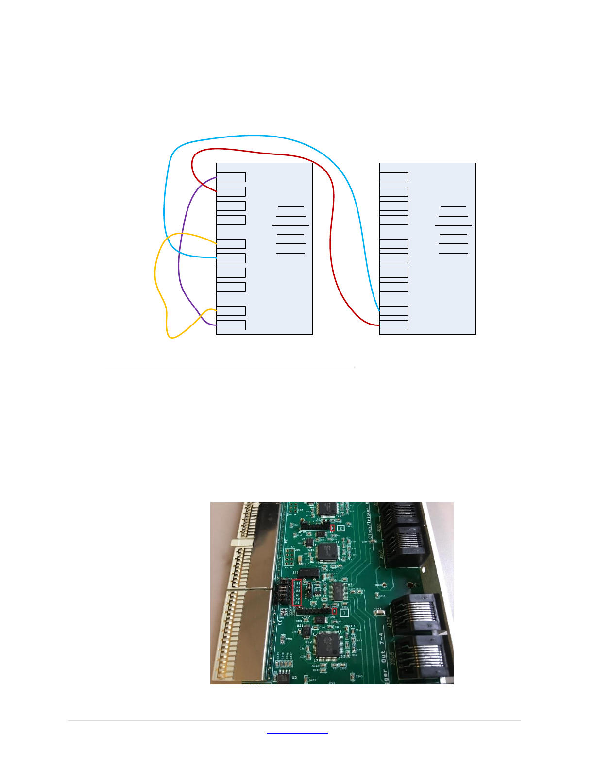
Figure 1-15 shows the cable connections between two Pixie-16 rear I/O trigger modules
that are installed in two separate crates. All connection cables are Category 5 or 6 Ethernet
cables and shall have the same length to minimize clock phase difference between Pixie16 modules in the two crates.
Figure 1-15: Cable connections between two Pixie-16 rear I/O trigger modules.
Jumper Settings on the Pixie-16 Rear I/O Trigger Modules
Trigger module #1 is installed in the rear slot #2 of crate #1. As mentioned earlier, the rear
slot #2 is located at the back of the crate and is at the direct opposite side of the front slot
#2 of the crate. Care should be taken when installing the trigger module into the rear slot
#2 by avoiding bending any pins of the rear side of the backplane, since that could cause
the 3.3V pin to be shorted to neighboring ground pin and thus damage the whole backplane.
Please note pin numbering for all jumpers on the trigger module is counted from right to
left when facing the top side of the module, i.e. the backplane connectors J3 to J5 are on
the left (only exception is JP1, which is in vertical orientation and should be counted from
bottom to top). A tiny ‘1’ label is painted on the right hand side of the jumpers, indicating
pin 1. Figure 1-16 shows the pin ‘1’ in red boxes.
Figure 1-16: Pin numbering for the jumpers on the Pixie-16 rear I/O trigger module.
Version 3.00 www.xia.com 26
Page 27

Pixie-16 User Manual August 21, 2018
JP1
Connect pins 1 and 2 for “P16”
JP20
Connect pins 2 and 3, 6 and 7
JP40
Connect pins 2 and 3, 6 and 7
JP60
Connect pins 1 and 2, 7 and 8
JP21
Connect pins 2 and 3
JP41
Connect pins 2 and 3
JP61
Connect pins 1 and 2
JP100
Connect pins 2 and 3 (connect to J4)
JP101
Connect pins 2 and 3 (connect to J4)
JP102
Connect pins 2 and 3 (connect to J4)
JP103
Connect pins 2 and 3 (connect to J4)
JP104
Connect pins 2 and 3 (connect to J4)
JP105
Connect pins 2 and 3 (connect to J4)
JP1
Connect pins 2 and 3 for “loc”
JP20
Connect pins 1 and 2, 7 and 8
JP40
Connect pins 1 and 2, 7 and 8
JP60
Connect pins 2 and 3, 6 and 7
JP21
Don’t connect any pin
JP41
Don’t connect any pin
JP61
Connect pins 1 and 2
JP100
Connect pins 2 and 3 (connect to J4)
JP101
Connect pins 2 and 3 (connect to J4)
JP102
Connect pins 2 and 3 (connect to J4)
JP103
Connect pins 2 and 3 (connect to J4)
JP104
Connect pins 2 and 3 (connect to J4)
JP105
Connect pins 2 and 3 (connect to J4)
Table 1-14 shows the jumper settings of the Pixie-16 rear I/O trigger module #1 in a 2crate system.
Table 1-14 Pixie-16 Rear I/O Trigger Module #1’s Jumper Settings
Trigger module #2 is installed in the rear slot #2 of crate #2. Table 1-15 shows the jumper
settings of the Pixie-16 rear I/O trigger module #2 in a 2-crate system.
Table 1-15 Pixie-16 Rear I/O Trigger Module #2’s Jumper Settings
Version 3.00 www.xia.com 27
Page 28

Pixie-16 User Manual August 21, 2018
J200
J201
J202
J203
J204
J205
J206
J207
J209
J208
Trigger
board #1
installed in
the rear
slot #2 of
Crate #1
Trigger
board #2
installed in
the rear
slot #2 of
Crate #2
Trigger
board #3
installed in
the rear
slot #2 of
Crate #3
Trigger
board #4
installed in
the rear
slot #2 of
Crate #4
J200
J201
J202
J203
J204
J205
J206
J207
J209
J208
J200
J201
J202
J203
J204
J205
J206
J207
J209
J208
J200
J201
J202
J203
J204
J205
J206
J207
J209
J208
Figure 1-17: Cable connections among four Pixie-16 rear I/O trigger modules.
Please note, if there are a total of four crates, the cable connections among those four Pixie16 rear I/O trigger modules that are installed in those four separate crates should follow the
connection methods shown in Figure 1-17. For the jumper settings on the Pixie-16 rear I/O
trigger modules, trigger module #1 and #2 should use the same jumper settings as those in
the trigger module #1 and #2 of the 2-crate system (Table 1-14 and Table 1-15),
respectively, whereas trigger module #3 and #4 should use the same jumper settings as
those in trigger module #2 (Table 1-15).
1.7.2 Trigger Distribution and Run Synchronization
In addition to distributing the global clock signal, the Pixie-16 rear I/O trigger module can
also share global triggers and run synchronization signals. The global trigger signals
include the global validation trigger and global fast trigger, plus the Pixie-16 FPGA data
storage buffers’ full flag signal. The run synchronization signals include synchronous run
start and stop signals that can be shared among multiple crates.
Version 3.00 www.xia.com 28
Page 29

Pixie-16 User Manual August 21, 2018
In order to enable the distribution of such global triggers and run synchronization signals,
certain Pixie-16 parameters have to be set properly. The parameter that controls the trigger
distribution and run synchronization is the Module Control Register B (ModCSRB).
ModCSRB is a 32-bit parameter with each of 32 bits controlling different operation modes
of the Pixie-16 module.
For the System Director module that is installed in the Master crate, bits 0, 4, 6 and 11 of
ModCSRB should be set to 1 (checked & enabled), as illustrated in Figure 1-18.
Figure 1-18: ModCSRB bit settings for the System Director Module in the Master crate.
For the Crate Master module that is installed in the Slave crate, bits 0, 6 and 11 of
ModCSRB should be set to 1 (checked & enabled), as illustrated in Figure 1-19.
Figure 1-19: ModCSRB bit settings for the Crate Master Module in the Slave crate.
For the General modules that are installed in both the Slave crate and Master crate, bit 11
of ModCSRB should be set to 1 (checked & enabled), as illustrated in Figure 1-20.
Figure 1-20: ModCSRB bit settings for the General Modules in both Master and Slave crates.
Version 3.00 www.xia.com 29
Page 30

Pixie-16 User Manual August 21, 2018
Use studs
at both
sides of the
crate to lift
it up in
order to
facilitate
air flow
from the
bottom.
2 Installation
2.1 Hardware Setup
A Pixie-16 system typically consists of a custom 14-slot 6U PXI crate, one or more Pixie16 modules, a crate controller, and accessories. The system is shipped out of the factory in
a large wooden box. We recommend proper storage of this wooden box after unpacking,
just in case there is a need to return the crate to factory for service or repair (the nails that
were used to seal the box are reusable).
When unpacking the Pixie-16 system, please be sure to collect the following items from
the wooden box:
1) The 14-slot 6U PXI crate
2) Power cord for the crate as well as VME version manual for the crate
3) Pixie-16 module(s)
4) Crate controller cards to be installed in the crate’s slot #1 and computer’s PCI slot
5) BNC-to-SMB cables
6) 2mm shunts for changing jumper settings on the Pixie-16 modules
A picture of a typical Pixie-16 digital data acquisition system is shown in Figure 2-1.
Figure 2-1: A typical Pixie-16 digital data acquisition system.
The Pixie-16 modules must be operated in this custom 6U CompactPCI/PXI crate which
provides high currents at specific voltages that are not included in the CompactPCI/PXI
Version 3.00 www.xia.com 30
Page 31

Pixie-16 User Manual August 21, 2018
standard. Of the 5 backplane connectors available in a 6U format, the lower two (J1, J2)
are defined by the CompactPCI/PXI standard, providing basic supply voltages, PCI host
I/O, and basic trigger connections. Pixie-16 modules follow this standard and are thus
compatible with any CompactPCI/PXI module that uses these two connectors only. The
upper three connectors (J3, J4, J5) are undefined in the CompactPCI/PXI standard. On
Pixie-16 modules, these connectors are used for custom power supplies with high currents
(1.8V, 5.5V, 3.3V) and for extended trigger distribution. Third party modules or crate using
the upper three connectors are most likely not compatible with Pixie-16 modules.
The AC power cords that come with the crates have North America NEMA 5-15 style
power plugs on one of the two ends (the other end plugs into the back of the crate) with
two flat parallel blades and one ground pin (one example of such power plug is shown in
Figure 2-2 top). For non-North America customers, it might be necessary to either find a
power socket that is compatible with the NEMA 5-15 style power plugs, or replace the
NEMA 5-15 style power plug with the one that is the standard in the customer’s country.
The replacement can be done by unscrewing the two nails on the NEMA 5-15 style power
plug, disconnecting the three wires from the plug (example of exposed wires shown in
Figure 2-2 bottom), and then connecting the wires to a new plug chosen by the customer.
Figure 2-2: An example of the NEMA 5-15 style power plug that come with the Pixie-16 crate and
inside look.
The Pixie-16 crate can be controlled either by a remote controller or embedded controller
(computer). If using a remote controller, first install the PC hardware of the PCI Bridge in
the host PC, and then install the PXI card into slot #1 (the one in red color in most crates)
of the crate, and finally connect these PCI bridge cards using the supplied copper or fiber
optic cable. If using an embedded controller, install it into slot #1 of the crate and no
external connections are required (besides mouse, keyboard and monitor).
Place the Pixie-16 modules into any peripheral PXI slot with the crate still powered down,
and then power up the crate, since the Pixie-16 modules are not hot swappable. If using a
remote controller, be sure to boot the host computer after powering up the crate. In Linux
systems, reloading the drivers for the Pixie-16 manually might be necessary if it is not done
automatically.
Version 3.00 www.xia.com 31
Page 32

Pixie-16 User Manual August 21, 2018
Connect the detector or preamplifier outputs to the SMB analog inputs of the Pixie-16.
SMB-BNC adapter cables are provided by XIA for each module. Make sure to set the input
termination appropriately to either 50 Ohm or High-Z by installing or removing,
respectively, the jumper on each channel located behind the Pixie-16 front panel before
installing the module in the crate.
2.2 Software Installation in Windows
The Pixie-16 Windows software includes the firmware files and DSP code files required
to configure a module, Windows drivers and a Visual Basic graphical user interface. All
files are included on the distribution CD-ROM (or via download from XIA’s web site) and
can be installed by running the installation program Setup.exe. Follow the instructions
shown on the screen to install the software to the default folder selected by the installation
program, or to a custom folder. This folder will contain 7 subfolders named Doc, Drivers,
DSP, Firmware, MCA, PulseShape, and Resources. Make sure you keep this folder
organization intact, as the interface program and future updates rely on this. Feel free,
however, to add folders and subfolders for the output data at your convenience.
After the software installation is completed, turn on the power to the crate, and then reboot
the computer. The Pixie-16 modules should appear as “PLX Custom (OEM) PCI 9054
Board” in Windows’ Device Manager (Figure 2-3). Otherwise, if Windows asks for drivers
for the Pixie-16 modules, please point to the PlxSdk.inf file in the “Drivers” sub-folder
under the Pixie-16 software installation folder, e.g. “C:\Program Files\XIA\Pixie16_VB
2.1.0\Drivers”. If there is still a PLX driver issue after the aforementioned software
installation steps, please go to XIA’s web site http://support.xia.com/default.asp?W372 to
download and install the PLX SDK V7.10.
Version 3.00 www.xia.com 32
Page 33

Pixie-16 User Manual August 21, 2018
Figure 2-3: Pixie-16 modules shown as “PLX Custom (OEM) PCI 9054 Board” in Windows’
Device Manager.
2.3 Software Installation in Linux
The Pixie-16 is fully supported in Linux operating systems. The Pixie-16 software for
Linux is built upon two sets of libraries. The first library is the API library provided by
PLX Technology, Inc. (now part of Avago Technologies). The PLX API library, also called
PLX Software Development Kit (SDK), provides functions that can be used to perform
read or write operations between the Pixie-16 hardware and the Linux computer through
the PCI bus (32-bit; 33 MHz) and the PCI 9054 I/O Accelerator from PLX Technology
Inc. The PLX PCI 9054 is a 32-bit PCI bus mastering interface chip that is built onto the
Pixie-16 hardware. The second library is the XIA Pixie-16 Application Programming
Interface (API), which consists of a set of C functions for building various data acquisition
applications utilizing the Pixie-16 modules. Complete source codes for both libraries are
Version 3.00 www.xia.com 33
Page 34

Pixie-16 User Manual August 21, 2018
provided so that the libraries can be complied under most commonly used Linux
distributions, such as RedHat or Fedora. Source codes for both libraries can be downloaded
from the following link: http://support.xia.com/default.asp?W372. Please follow the
instructions included in the libraries to compile and test them in the Linux environment.
2.4 Getting Started
This section describes the basic steps to get initial list mode traces or MCA histograms
with the Pixie-16 system in a Windows software environment. For detailed introduction to
the software interface, refer to section 3.
After installation, find the shortcut Pixie16_VB on your desktop and start it with a double
click. You can also directly run the file Pixie_VB.exe in the installation folder.
The user interface consists of a left control bar with 4 tabs: Startup, Settings, Run, and
Results, as shown in Figure 2-4. The area to the right will display control panels or graphs.
The top menu bar contains links to some frequently used result displays as well as some
advanced parameter tables.
Figure 2-4: The Pixie -16 Windows software user interface.
2.4.1 Startup
To boot the modules, select the default Startup tab. First, enter the number of modules and
specify the module’s slot numbers. You can click on the [Select Configuration Files]
button to verify the boot files and paths are pointed to the correct installation folder. Then
Version 3.00 www.xia.com 34
Page 35

Pixie-16 User Manual August 21, 2018
click on the button [Boot Pixie-16 Modules]. The bottom
status line should show a green marker indicating that the
Pixie-16 modules are initialized successfully. For offline
analysis only operation with no Pixie-16 modules installed,
check on the Offline Analysis box before booting.
2.4.2 Settings
To configure the modules for your detector, go to the Settings
tab. Click on the [Acquire ADC Traces] button to view the
input signal for either a single channel or for all 16 channels
of the Module selected at the bottom of the panel. Click on
[Refresh] to acquire untriggered traces that are read directly
from the ADC. You can adjust the sampling interval to see a
longer time period. Pulses from the detector should fall in the
range of the ADC with a positive amplitude, i.e. positive
going with a rising edge, and no clipping at the upper limit. If
the signal is not in range, click on the [Adjust Offsets] button
to let the software to automatically set the DC offsets, or you
could manually adjust the DC offset by clicking on the [Set
DAQ Parameter] button, then go to the Analog Signal
Conditioning tab and adjust the offset. While being there,
you can also adjust the gain and polarity of each channel.
A very critical parameter for the energy computation is the
signal decay time PREAMPTAU. In the SET DAQ
PARAMETER panel, go to the Decay Time tab to set this value.
You can either enter it directly for each channel, or enter an
approximate value in the right control, select a channel, and
click on [Find it] to let the software determine the decay time
automatically. In order for the software to successfully find
the decay time automatically, the channel should connect to a
detector output, and detector count rate should be reasonably
high (at least ~ 1Kcps). Otherwise, the automatic Tau finder
tool will time out and won’t return a PREAMPTAU value
successfully. In such case, the PREAMPTAU value will be
unchanged. If a PREAMPTAU value is indeed found
successfully, click on [Accept it] to apply the found value to
the channel.
When the signal is in range and the decay time is found, you
can store the parameters on file using the [Save Parameters]
button. Make sure to check the box for DSP settings to not
only save the GUI settings (such as slot numbers), but also
the DSP settings for each module (gain, offset, decay times,
etc.). The settings are called DSP settings since all DAQ
parameters are first downloaded to the DSP on the Pixie-16,
and then the DSP will decode the settings and download them
to the FPGAs.
2.4.3 Run
Version 3.00 www.xia.com 35
Page 36

Pixie-16 User Manual August 21, 2018
When the DSP settings have been set, at least initially, you can go to the Run tab to start a
test data acquisition run. Using the Run Type control, specify a list mode run to acquire
waveforms and MCA histograms, or a MCA mode run to only acquire histograms. Click
on [Start] to begin data acquisition.
The run can be stopped either by manually pressing the [Stop] button, or by the preset Run
time / time out condition (MCA or list mode run), or by the condition of reaching a preset
Number of FIFO fills in Module 0 (List mode run only). Here each FIFO fill corresponds
to approximately 128K list mode data words (32-bit per word).
To synchronize data acquisition runs in all Pixie-16 modules, check the option boxes of
both “Start/stop runs in all modules simultaneously?” and “Synchronize clocks in all
modules?”.
The output files are automatically saved into the MCA or PulseShape folder at the end of
the run, depending which run type is chosen. The output file names can be specified in the
boxes of “Base name” and “Run number”. If output files should not be overwritten in
subsequent runs, the option “Auto increment run number” should be checked.
2.4.4 Results
After the run, statistics, spectra or traces can be viewed by
selecting the corresponding item from the Results tab. The
data is also saved to files that can be imported into other
analysis software.
The run statistics results are organized as three columns for
each channel, i.e. Live Time, ICR (input count rate) and OCR
(output count rate). By changing the Module Number at the
top of the Results tab, each module’s run statistics can be
viewed. The Processed events box on the Results tab is not in
use currently. The Real time box displays the real time for the
previous data acquisition run. The real time starts counting
when the run is started and stops when the run is stopped. So
it is similar to a wall clock time. The live time, on the other
hand, only counts when the Pixie-16 is actually processing
events and taking data. For instance, if run synchronization is
required among multiple Pixie-16 modules, the real time will
start counting when each module is issued a run-start
command, but the live time will not start counting until the
last module finishes its run initialization routines in the DSP
and all modules start data acquisition synchronously. In such
case, the live time will be smaller than the real time.
The MCA Spectrum can be viewed and inspected by clicking
on the [Show MCA Spectrum] button. On the MCA
SPECTRUM DISPLAY panel, single channel or 16-channel’s MCA spectra can be viewed and
analyzed. The peak position, energy resolution (FWHM), and peak area can be obtained
by choosing the ROI (region of interest) on the spectrum.
The List Mode Traces can be viewed and inspected by clicking on the [Show List Mode
Traces] button. On the LIST MODE TRACES DISPLAY panel, single channel or 16-channel’s
list mode traces can be viewed and analyzed. By selecting the event number for the events
stored in the list mode data file, each event’s energy, timestamp, and trace can be displayed.
Version 3.00 www.xia.com 36
Page 37

Pixie-16 User Manual August 21, 2018
3 Navigating the Pixie-16 User Interface
3.1 Overview
The Pixie-16 graphical user interface (Figure 2-4) provides a user a simple tool to control
the Pixie-16 cards. It was written using Microsoft’s Visual Basic programming language
and its underlying function calls are directed to two dynamic link library (DLL) files,
Pixie16AppDLL.dll and Pixie16SysDLL.dll. Those users who are interested in learning
more about these DLLs can read the Programmer’s Manual. The user interface consists of
a work area where DAQ graphs, tables and panels are to be shown, a control bar to the left
which contains four tabs with control buttons (Startup, Settings, Run, and Results), and
status indicators at the bottom. Below we describe the steps of using this interface.
3.2 Startup
After the user interface is launched, the user will see the window with the default Startup
tab selected in the control bar. Enter the number of modules and specify the module’s slot
numbers as labeled on the crate. You can click on the [Select Configuration Files] button
to open the CONFIGURATION FILES & OUTPUT DATA PATHS panel (Figure 3-1) and verify
that the boot files and paths are pointed to the correct folder. You can directly input the file
name in the boxes, or use the file open icon at the right end of each line to locate a specific
file.
Usually, users need only change the DSP parameters file to load alternative settings (same
as [Loading Parameters] in the Setting tab) or change the Output Data Paths to direct the
output data into a custom location. However, if you receive firmware updates or custom
firmware from XIA, you can click on the [Select FPGA Firmware Files] button or the
[Select DSP Code Files] button to select which FPGA or DSP file to use.
Figure 3-1: The Pixie -16 configuration files & output data paths panel.
When the files and paths are set correctly, click on the button [Boot Pixie-16 Modules].
The bottom status line should show a green marker indicating that the Pixie-16 modules
have been initialized successfully. If one or more modules failed to boot, click on the [Log]
Version 3.00 www.xia.com 37
Page 38

Pixie-16 User Manual August 21, 2018
button to view a series of diagnostic messages. The messages are also stored in a file called
“Pixie16msg.txt” and can be sent to XIA when requesting customer support. This log file
is located in the same folder as the user interface program Pixie16_VB.exe.
For analysis-only operation with no modules connected, check the Offline Analysis box
before booting. In offline mode, the user can still access every button or control of the
interface. Results from previous acquisitions can also be viewed by loading the results files.
3.3 Settings
The operation of the Pixie-16’s on-board DSP is controlled by a variety of parameters.
They can be set using the SET DAQ PARAMETERS panel, opened by clicking on the [Set
DAQ Parameters] button in the Settings tab. The panel has 12 tabs, as shown in Figure
3-2.
Figure 3-2: The Pixie -16 set DAQ parameters panel.
Using the button in the left control bar, DAQ parameters can be:
Copied from one channel to some or all channels and modules in the system. When
copying, first select source module and channel at the top of the copy panel, then select the
items to copy on the left (corresponding to the 12 tabs of the SET DAQ PARAMETERS
panel), then select the destination channels and modules, and finally click on the [Copy]
button.
Saved to disk. When saving, make sure to check the box for DSP settings.
Loaded from disk.
Version 3.00 www.xia.com 38
Page 39

Pixie-16 User Manual August 21, 2018
3.3.1 Filter
The Filter tab shows the settings for the energy filter which measures the pulse height and
for the trigger filter which detects pulses. The filtering principle is described in section 6.
General rules of thumb for the following important parameters are:
1. The energy filter flat top time should be larger than the longest pulse rise time.
2. The energy filter rise time can be varied to balance the resolution and throughput.
In general, energy resolution improves with the increase of energy filter rise time,
up to an optimum when longer filters only add more noise into the measurement.
The energy filter dead time TD is about 2 × (T
throughput for Poisson statistics is 1/(TD*e). For HPGe detectors, a rise time of 46s and a flat top of 1s are usually appropriate.
3. A longer trigger filter rise time averages more samples and thus allows setting
lower thresholds without triggering on noise.
4. Typically the threshold should be set as low as possible, just above the noise level.
The remaining parameters are usually minor adjustments for fine tuning and otherwise can
remain at the default values:
5. A longer trigger filter flat top time makes it easier to detect slow rising pulses.
6. Choose the smallest energy filter range that allows setting the optimum energy
filter rise time. Larger filter ranges allow longer filter sums, but increase the
granularity of possible values for the energy filter rise time and flat top time and
increase the jitter of latching the energy filter output relative to the rising edge of
the pulse. This is usually only important for very fast pulses.
rise
+ T
), and the maximum
flat
3.3.2 Analog Signal Conditioning & Acquire ADC Traces
The Analog Signal Conditioning tab controls the analog gain, offset and polarity for each
channel. It is useful to click on the [Acquire ADC Traces] button in the left control bar to
view the signal that is read from the ADCs while adjusting these parameters (see Figure
3-3). The display shows all 16 channels of a module in 4 graphs of 4, and the sampling
interval for each block can be set to capture a longer time frame. Click on the [refresh]
button to update the graph.
Pulses from the detector should fall in the range of the ADC, e.g. from 0 to 4095 for a 12bit ADC, with the baseline at ~10% of the ADC range (i.e. ~400) to allow for drifts,
undershoots or mirror charges and no clipping at the upper limit. If there is clipping, adjust
the Gain and Offset or click on the [Adjust Offsets] button to let the software set the DC
offsets to proper levels automatically.
Since the trigger/filter circuits in the FPGA only act on rising pulses, negative pulses are
inverted at the input of the FPGA, and the waveforms shown in the ADC trace display
include this optional inversion. Thus, it is important to set the channel’s Polarity such that
pulses from the detector appear with positive amplitude (rising edge).
In the ADC trace - single channel tab, the ADC trace display also includes the option to
view a FFT of the acquired trace. This is useful to diagnose noise contributions. Above the
graph are controls for cursors and an option to change between linear and log scale. You
can also save a trace to a text file using the disk symbol at the right.
Version 3.00 www.xia.com 39
Page 40

Pixie-16 User Manual August 21, 2018
Figure 3-3: The Pixie -16 Set DAQ Parameters panel and ADC trace display.
3.3.3 Histogram Control
The binning factor in the Histogram Control tab controls the number of MCA bins in the
spectrum. Energies are computed as 16-bit numbers, allowing in principle 64K MCA bins.
However, spectrum memory for each channel is limited to 32K bins, so computed energy
values are divided by 2
set to 1, but for low count rates and wide peaks, it might be useful to set it to a larger value
to obtain a spectrum with fewer bins, but more counts per bin.
Emin is reserved for a future function to subtract a constant “minimum energy” from the
computed energy value before binning to essentially cut off the lower end of the spectrum.
3.3.4 Decay Time
As mentioned previously in section 2.4.2, a critical parameter for pulse energy computation
is the signal decay time Tau. At high count rates, pulses overlap with each other at higher
frequency. In order to compute the energy or pulse height of those pulses accurately
without the need to wait until they decay back to baseline level completely, the pulse height
computation algorithm implemented in the Pixie-16 uses the decay time to compute and
remove the contribution from the exponentially decaying tail of the overlapping prior pulse
when computing the pulse height of the current pulse.
It is assumed the pulses have only a single exponential decay constant. If pulses have
multiple decay constants, it might be possible to use the decay constant that dominates the
decay of the pulse, but the accuracy of pulse height computation will be degraded.
binning factor
before building the histogram. Binning factor is usually
3.3.5 Pulse Shape Analysis
In the Pulse Shape Analysis tab, you can set the total trace length and the pre-trigger trace
delay for the waveforms to be acquired in list mode runs. The trace delay cannot be longer
Version 3.00 www.xia.com 40
Page 41

Pixie-16 User Manual August 21, 2018
Bit name
Bit #
Description
MODCSRB_CPLDPULLUP
0
Enable pullups for PXI trigger lines on the backplane through an
onboard CPLD. With the pullups, those PXI trigger lines default
to logic high state. Only when one module actively pulls a line to
logic low state will such a line be in the low state. Therefore
signals transmitted over those PXI trigger lines are actively low
signals
Note: enable this bit only for one module per crate (e.g. the
crate master module)
reserved
3:1
MODCSRB_DIRMOD
4
Set this module as the Director module so that it can send triggers,
trace and header DPM full signal and run synchronization signal
to all crates through the rear I/O trigger modules. Here triggers
include fast trigger and validation trigger
than the trace length, and for each Pixie-16 variant, there is also a limit for the maximum
value of trace delay and trace length.
For the 500 MHz Pixie-16 modules, the ADCs are running at 500 MHz, but the traces are
recorded with 100 MHz clocks in the FPGA with 5 ADC samples captured in each 10 ns
interval. In addition, the data packing from the FPGA to the onboard External FIFO is two
sets of 5 ADC samples in one transfer. So the trace length should be multiples of 20 ns,
i.e., 20 ns, 40 ns, … for instance, a trace length of 500 ns and a trace delay of 200 ns.
3.3.6 Baseline Control & Acquire Baselines
The Pixie-16 constantly takes baseline measurements when no pulse is detected and keeps
a baseline average to be subtracted from the energy filter output during pulse height
reconstruction. Baseline measurements that differ from the average by more than the
Baseline Cut value will be rejected as they are likely contaminated with small pulses below
the trigger threshold. A series of baseline measurements for each channel can be viewed
by clicking on the [Acquire Baseline] button, and in the BASELINE - SINGLE CHANNEL
panel a histogram of baselines can be built to verify that the Baseline Cut does not reject
measurements falling into the main (ideally Gaussian) peak in the baseline distribution.
Usually, it is sufficient to keep Baseline Cut at its default value.
Note: Since the baseline computation takes into account the exponential decay, no pulses
should be noticeable in the baseline display if a) the decay time is set correctly and b) the
detector pulses are truly exponential.
Baseline Percent is a parameter used for automatic offset adjustment; by clicking on the
Adjust Offsets button, offsets will be set such that the baseline seen in the ADC trace display
falls at the Baseline Percent fraction of the full ADC range (e.g. for a 12-bit ADC and
Baseline Percent = 10% the baseline falls at ADC step 409 out of 4096 total).
3.3.7 Control Registers
The Control Registers tab sets a number of options affecting the module as a whole
(Module Control Register B) or affecting each channel individually (Channel Control
Register A):
Module Control Register B
Table 3-1 Descriptions of Module Control Register B
Version 3.00 www.xia.com 41
Page 42

Pixie-16 User Manual August 21, 2018
Note: enable this bit only for one module among all crates (e.g.
the system director module in multi-crate configuration)
reserved
5
MODCSRB_CHASSISMASTER
6
Set this module as the chassis master module so that it can send
triggers, trace and header DPM full signal and run
synchronization signal to the backplane of the local crate. Here
triggers include fast trigger and validation trigger
Note: enable this bit only for one module per crate (e.g. the
crate master module)
MODCSRB_GFTSEL
7
Select external fast trigger source (=1: external validation trigger,
=0: external fast trigger, in case these two signals are swapped at
the Pixie-16 front panel input connectors)
MODCSRB_ETSEL
8
Select external validation trigger source (=1: external fast trigger,
=0: external validation trigger, in case these two signals are
swapped at the Pixie-16 front panel input connectors)
reserved
9
MODCSRB_INHIBITENA
10
Enable (=1) or disable (=0) the use of external INHIBIT signal.
When enabled, the external INHIBIT signal in the logic high state
will prevent the run from starting until this external INHIBIT
signal goes to logic low state
MODCSRB_MULTCRATES
11
Set this module to run in the multi-crate mode (=1) or in the localcrate mode (=0). If the module is running in multi-crate mode, it
will use the trace and header DPM full signal and run
synchronization signal that are generated and distributed among
multiple crates. If the module is running in local-crate mode, it
will use the trace and header DPM full signal and run
synchronization signal generated in the local crate
MODCSRB_SORTEVENTS
12
Sort (=1) or do not sort (=0) events from all 16 channels of a
Pixie-16 module based on the timestamps of the events, before
storing the events in the external FIFO
Note: all 16 channels must have the same DAQ parameters
setting to use this feature
MODCSRA_BKPLFASTTRIG
13
Enable (=1) or disable (=0) the sending of 16 local fast triggers to
the 16 lines on the backplane of the crate
Note: only one module can enable this option in each PCI bus
segment of a crate (not limited to the crate master module, e.g.
any module in each PCI bus segment)
reserved
31:14
Bit name
Bit #
Description
CCSRA_FTRIGSEL
0
Channel fast trigger selection (=1: module fast trigger from the
System FPGA; =0: the selection depends on the value of another
bit CCSRA_GROUPTRIGSEL – if CCSRA_GROUPTRIGSEL
= 1, select the channel validation trigger from the System FPGA,
Channel Control Register A
Table 3-2 Descriptions of Channel Control Register A
Version 3.00 www.xia.com 42
Page 43

Pixie-16 User Manual August 21, 2018
and if CCSRA_GROUPTRIGSEL = 0, select this channel’s local
fast trigger)
CCSRA_EXTTRIGSEL
1
Module validation trigger selection (=1: module gate input from
the Pixie-16 front panel Module Gate LVDS connector; =0:
module validation trigger from the System FPGA)
CCSRA_GOOD
2
Set this channel as a Good channel (=1) or a not Good channel
(=0). When a channel is set to be a not Good channel, it still
generates local fast triggers, which could be used in multiplicity
computation, etc., but this channel will not record list mode data
or MCA data, and will not update its baseline value
CCSRA_CHANTRIGSEL
3
Channel validation signal selection (=1: channel gate input from
the Pixie-16 front panel Channel Gate LVDS connector; =0:
channel validation trigger from the System FPGA)
CCSRA_SYNCDATAACQ
4
Choose the level of synchronous data acquisition for this channel
(=1: stops taking data when the trace or header DPM for any
channel of any Pixie-16 module in the system is full; =0: stops
taking data only when the trace or header DPM for this channel
of this Pixie-16 module is full)
CCSRA_POLARITY
5
Choose this channel’s input signal polarity (=1: invert input
signal’s polarity; =0: do not invert input signal’s polarity).
(Please note in Pixie-16, signal processing requires positive rising
input signal. So if input signal has a negative falling edge, it
should be inverted by setting this CCSRA_POLARITY bit to 1)
CCSRA_VETOENA
6
Enable (=1) or disable (=0) this channel’s veto. If veto is enabled,
this channel’s fast trigger will be vetoed by either the module
veto signal (see bit 20 CCSRA_MODVETOSEL below) or
channel veto signal (see bit 19 CCSRA_CHANVETOSEL
below). But if veto is disabled, this channel’s fast trigger will not
be vetoed by either veto signal, even if either veto signal is
present
CCSRA_HISTOE
7
Enable (=1) or disable (=0) the histogramming of pulse energy
values in the onboard MCA memory. However, the current Pixie16 firmware always histograms pulse energy values in the
onboard MCA memory. So this CCSRA_HISTOE is essentially
not in use at the moment
CCSRA_TRACEENA
8
Enable (=1) or disable (=0) trace capture in the list mode run for
this channel
CCSRA_QDCENA
9
Enable (=1) or disable (=0) QDC sums recording in the list mode
run for this channel. There are a total of 8 QDC sums for each
event
CCSRA_CFDMODE
10
Enable (=1) or disable (=0) CFD trigger in the list mode run for
this channel. CFD trigger is used to latch sub-sample timing for
the event time of arrival or timestamp
CCSRA_GLOBTRIG
11
Enable (=1) or disable (=0) the requirement of module validation
trigger (see 3.3.11.5) for this channel. If enabled, only when
module validation trigger overlaps the channel fast trigger will
the events be recorded for this channel
CCSRA_ESUMSENA
12
Enable (=1) or disable (=0) the recording of raw energy sums and
baseline values in the list mode run for this channel. There are a
Version 3.00 www.xia.com 43
Page 44

Pixie-16 User Manual August 21, 2018
total of three raw energy sums and one baseline value for each
event. Please note the baseline value is stored in the format of 32bit IEEE float point (IEEE 754)
CCSRA_CHANTRIG
13
Enable (=1) or disable (=0) the requirement of channel validation
trigger (see 3.3.11.4) for this channel. If enabled, only when
channel validation trigger overlaps the channel fast trigger will
the events be recorded for this channel
CCSRA_ENARELAY
14
Switch between two attenuations or gains for the input signal in
this channel through an input relay (=1: close the input relay
resulting in no input signal attenuation; =0: open the input relay
resulting in a ¼ input signal attenuation)
CCSRA_PILEUPCTRL
15
Control normal pileup rejection (bit 15) and inverse pileup
rejection (bit 16) for list mode runs:
1) Bits [16:15] = 00, record all events
2) Bits [16:15] = 01, only record single events, i.e., reject
piled up events
3) Bits [16:15] = 10, record everything for piled up events,
but will not record trace for single events even if trace
recording is enabled, i.e., only record event header
4) Bits [16:15] = 11, only record piled up events, i.e., reject
single events
In all cases, if the event is piled up, no energy will be computed
for such event
CCSRA_INVERSEPILEUP
16
CCSRA_ENAENERGYCUT
17
Enable (=1) or disable (=0) the “no traces for large pulses”
feature. If enabled, trace will be not be recorded if the event
energy is larger than the value set in DSP parameter EnergyLow
CCSRA_GROUPTRIGSEL
18
Select channel fast trigger – this bit works together with the
CCSRA_FTRIGSEL bit (bit 0): if CCSRA_FTRIGSEL= 1, this
CCSRA_GROUPTRIGSEL bit has no effect; if
CCSRA_FTRIGSEL= 0, then if CCSRA_GROUPTRIGSEL = 1,
select the channel validation trigger from the System FPGA, and
if CCSRA_GROUPTRIGSEL = 0, select this channel’s local fast
trigger
CCSRA_CHANVETOSEL
19
Channel veto signal selection (=1: channel validation trigger from
the System FPGA; =0: channel gate input from the Pixie-16 front
panel Channel Gate LVDS connector)
CCSRA_MODVETOSEL
20
Module veto signal selection (=1: module validation trigger from
the System FPGA; =0: module gate input from the Pixie-16 front
panel Module Gate LVDS connector)
CCSRA_EXTTSENA
21
Enable (=1) or disable (=0) the recording of the 48-bit external
clock timestamp in the event header during list mode run for this
channel
reserved
31:22
Version 3.00 www.xia.com 44
Page 45

Pixie-16 User Manual August 21, 2018
)(
)1*2()1(
][][][
FGFLi
FGFLij
i
FLij
jTracejTraceiFF
][)8/1(*][][ iFFwDiFFDiCFD
CFDout2CFDout1
CFDout1
f
N
CFDout2CFDout1
CFDout1
CFD
3.3.8 CFD Trigger
3.3.8.1 100 MHz and 250 MHz Pixie-16 modules
The following CFD algorithm is implemented in the signal processing FPGA of the 100
MHz (Rev. B, C, D and F) and 250 MHz (Rev. F) Pixie-16 modules. Assume the digitized
waveform can be represented by data series Trace[i], i = 0, 1, 2, … First the fast filter
response (FF) of the digitized waveform is computed as follows:
(3-1)
Where FL is called the fast length and FG is called the fast gap of the digital trapezoidal
filter. Then the CFD is computed as follows:
(3-2)
Where D is called the CFD delay length and w is called the CFD scaling factor (w=0, 1,
…, 7).
The CFD zero crossing point (ZCP) is then determined when CFD[i] 0 and CFD[i+1] <
0. The timestamp is latched at Trace point i, and the fraction time f is given by the ratio of
the two CFD response amplitudes right before and after the ZCP.
(3-3)
Where CFDout1 is the CFD response amplitude right before the ZCP, and CFDout2 is the
CFD response amplitude right after the ZCP (subtraction is used in the denominator since
CFDout2 is negative). The Pixie-16 DSP computes the CFD final value as follows and
stores it in the output data stream for online or offline analysis.
(3-4)
Where N is scaling factor, which equals to 32768 for 100 MHz modules and 16384 for 250
MHz modules, respectively (see 4.2.3.1).
Figure 3-4 shows a sample ADC trace, its fast filter response and its CFD response,
respectively. The top figure shows a raw ADC trace. After computing the fast filter
response on the raw ADC trace using Equation 3-1, the fast filter response is compared
against the fast filter threshold as shown in the middle figure. The ADC sample where the
fast filter response crosses the fast filter threshold is called the fast trigger point, which also
starts the search for the CFD zero crossing point. The CFD response is computed using
Equation 3-2 and is shown in the bottom figure (for actual implementation in the firmware,
the fast filter response FF is delayed slightly before being used for computing the CFD
response so that there are sufficient number of CFD response points to look for the zero
crossing point after the fast trigger). To prevent premature CFD trigger as a result of the
noise in the CFD response before the actual trigger, a DSP parameter called CFDThresh is
used to suppress those noise-caused zero crossing. However, if a zero crossing point cannot
be found within a certain period after the fast trigger (typically 32 clock cycles), e.g., due
to unnecessarily high CFDThresh, a forced CFD Trigger will be issued and a flag will be
set in an event header word to indicate that the recorded CFD time for this event is invalid.
However, the event will still have a valid timestamp which is latched by the fast filter
Version 3.00 www.xia.com 45
Page 46

Pixie-16 User Manual August 21, 2018
CFD Parameters
DSP Parameters
FL
FastLength
FG
FastGap
Fast Filter Threshold
FastThresh
D
CFDDelay
W
CFDScale (valid values: 0, 1, 2, … and 7)
CFD Threshold
CFDThresh
trigger when fast filter crosses over the trigger threshold. The aforementioned CFD
parameters correspond to the following DSP parameters.
Table 3-3 Corresponding DSP Parameters for the CFD Parameters
Version 3.00 www.xia.com 46
Page 47

Pixie-16 User Manual August 21, 2018
LDk
Dki
LBDk
BDki
Lk
ki
LBk
Bki
iaiaiaiawkCFD
Figure 3-4: Illustration of the Pixie-16 CFD algorithm
In the 250 MHz Pixie-16 modules, the event timestamp is counted with 125 MHz clock
ticks, i.e., 8 ns intervals, and two consecutive 250 MHz ADC samples are captured in one
8 ns interval as well. The CFD trigger also runs at 125 MHz, but the CFD zero crossing
point is still reported as a fractional time between two neighboring 250 MHz ADC samples,
which are processed by the FPGA in one 125 MHz clock cycle. However, the CFD zero
crossing point could be in either the odd or even clock cycle of the captured 250 MHz ADC
waveforms. Therefore, the firmware outputs a "CFD trigger source" bit in the output data
stream to indicate whether the CFD zero crossing point is in the odd or even clock cycle of
the captured 250 MHz ADC waveforms.
In the 100 MHz Pixie-16 modules, event timestamp, CFD trigger, and ADC waveform
capture are all carried out with the same 100 MHz clock. So there is no need to report "CFD
trigger source" for the 100 MHz Pixie-16 modules.
3.3.8.2 500 MHz Pixie-16 modules
The CFD algorithm discussed in the previous section for the 100 MHz and 250 MHz Pixie16 modules can also be written in the following format:
(3-5)
Where a(i) is the ADC trace data, k is the index, and w, B, D, and L are CFD parameters.
The CFD algorithm implemented in the 500 MHz Pixie-16 modules is special when
compared to the one implemented in the 100 MHz and 250 MHz Pixie-16 modules in terms
of the ability to adjust parameters w, B, D, and L. The reason for this is that in the 500 MHz
Pixie-16 modules, ADC data that come into the FPGA at the speed of 500 MHz is first
slowed down with a ratio of 1:5, in other words, the FPGA captures 5 ADC samples at the
rate of 100 MHz, i.e., every 10 ns. The FPGA then tries to find the CFD trigger point
between any two adjacent 2-ns ADC samples within that 10 ns by first building sums of
Version 3.00 www.xia.com 47
Page 48

Pixie-16 User Manual August 21, 2018
CFD Parameters
Fixed Values for 500 MHz Modules
w
1
B
5
D
5
L
1
CFD Trigger
Source [2:0]
Zero Crossing Point (ZCP) Location
000
ZCP occurred between the 5th ADC sample of the previous 5-sample group
and the 1st ADC sample of the current 5-sample group
001
ZCP occurred between the 1th ADC sample of the current 5-sample group
and the 2nd ADC sample of the current 5-sample group
010
ZCP occurred between the 2nd ADC sample of the current 5-sample group
and the 3rd ADC sample of the current 5-sample group
011
ZCP occurred between the 3rd ADC sample of the current 5-sample group
and the 4th ADC sample of the current 5-sample group
100
ZCP occurred between the 4th ADC sample of the current 5-sample group
and the 5th ADC sample of the current 5-sample group
101
Not used
110
Not used
111
CFD trigger is forced, so CFD time is invalid
8192
CFDout2CFDout1
CFDout1
CFD
ADC samples and then calculating differences between delayed and non-delayed sums
until the zero crossing point is found. However, in the 500 MHz Pixie-16 modules, the
FPGA does not have enough resources to build sums for 5 ADC samples in parallel with
variable delays. Therefore, the CFD algorithm for the 500 MHz modules was implemented
using a set of fixed CFD parameters as shown in Table 3-4. Tests show these fixed
parameters give best performance for LaBr3(Ce) detectors.
Table 3-4 Fixed CFD Parameter Values for 500 MHz Pixie-16 Modules
The CFD time given by the 500 MHz Pixie-16 modules consists of two parts: a shift within
the 5 ADC samples and a fractional time between two ADC samples where the CFD zero
crossing occurred. The shift within the 5 ADC samples is reported as the 3-bit CFD trigger
source [2:0] is defined as follows.
Table 3-5 Meanings of the CFD Trigger Source for 500 MHz Pixie-16 Modules
The CFD fractional time is given as follows.
3.3.9 Trigger Stretch Lengths
External trigger stretch is used to stretch the module validation trigger pulse.
Channel trigger stretch is used to stretch the channel validation trigger pulse.
Veto stretch is used to stretch the veto pulse for this channel.
Fast trigger backplane length is used to stretch the fast trigger pulse to be sent to the
System FPGA, where this fast trigger can be sent to the backplane to be shared with other
modules, or can be used for making coincidence or multiplicity triggers.
Version 3.00 www.xia.com 48
(3-6)
Page 49

Pixie-16 User Manual August 21, 2018
Parameters
Range
100 or 500 MHz
250 MHz
External trigger stretch
0.01 – 40.95 µs
0.008 – 32.76 µs
Channel trigger stretch
0.01 – 40.95 µs
0.008 – 32.76 µs
Veto stretch
0.01 – 40.95 µs
0.008 – 32.76 µs
Fast trigger backplane length
0.01 – 40.95 µs
0.008 – 32.76 µs
External delay length
0 – 2.55 µs (Rev. B/C/D)
0 – 5.11 µs (Rev. F)
0 – 4.088 µs
Fast trigger backplane delay
0 – 2.55 µs (Rev. B/C/D)
0 – 5.11 µs (Rev. F)
0 – 4.088 µs
3.3.10 FIFO Delays
External delay length is used to delay the incoming ADC waveform and the local fast
trigger in order to compensate for the delayed arrival of the external trigger pulses, e.g.,
module validation trigger, channel validation trigger, etc.
Fast trigger backplane delay is used to delay the fast trigger pulse before it is sent to the
System FPGA for sharing with other modules through the backplane or making
coincidence or multiplicity triggers.
Table 3-6 Range for Trigger Stretch Lengths and FIFO Delays in Pixie-16 Modules
Figure 3-5 illustrates the signal processing in the Pixie-16 modules. The Trigger Stretch
Lengths and FIFO Delays discussed above are shown in number 1 to 6 in the figure.
Version 3.00 www.xia.com 49
Page 50

Pixie-16 User Manual August 21, 2018
Analog
In
ADC
Capture
FIFO
2
1024 × 16
Energy Filter
Trigger Filter
Pileup
Detector
D
S
P
B
U
S
System
FPGA
DSP
Signal Processing FPGA
Trace DPM
Rev. F3: 8192×32
Rev. B/C/D: 4096×32
Control
Logic
Header DPM
Rev. F: 512×64
Rev. B/C/D: 512×32
Event Header
Information
(Timestamp,
Energy, QDC
sums, etc.)
External FIFO
(256K × 18)
Delay FIFO
1
Status
Registers
PCI
Interface
Host
Computer
Fast Filter
(generate fast trigger and
stretch to pulse)
CFD
QDC
Latch
Module Veto
Delay FIFO
Rev. F: 512×1
Rev. B/C/D: 256×1
Channel Veto
Latch
Channel Validation Trigger (x16)
stretch to pulse
stretch to pulse
Module Validation Trigger (x1)
stretch to pulse
❶
❷
❸
❹
❺
❻
❶ - Fast trigger backplane length (FastTrigBackLen)
❷ - Fast trigger backplane delay (FtrigoutDelay)
❸ - Extern delay length (ExternDelayLen)
❹ - External trigger stretch length (ExtTrigStretch)
❺ - Channel trigger stretch length (ChanTrigStretch)
❻ - Veto stretch (VetoStretch)
FT_back - Fast trigger sent
to the System FPGA for
making coincidence and
multiplicity triggers or
sharing with other modules
(From front panel)
Module Fast Trigger (x1)
Latch
Ftrig_sel
ModVeto_sel
ChanVeto_sel
Latch
Latch
OR
Ftrig_sel --
CHANCSRA[0] = 1: use latched module fast trigger
CHANCSRA[0] = 0 & CHANCSRA[18] = 1: use latched channel validation trigger
CHANCSRA[0] = 0 & CHANCSRA[18] = 0: use local fast trigger
ChanVeto_sel --
CHANCSRA[19] = 1: use Channel Validation Trigger from System FPGA
CHANCSRA[19] = 0: use Channel Veto from front panel
ModVeto_sel --
CHANCSRA[20] = 1: use Module Validation Trigger from System FPGA
CHANCSRA[20] = 0: use Module Veto from front panel
1
For the Delay FIFO to set the extern delay
length, its length is either 2.55 µs (Rev. B/C/D)
or 5.11 µs (Rev. F, 100 MHz) or 4.088 µs (Rev.
F, 250 MHz) or 5.11 µs (Rev. F, 500 MHz)
2
For 250 MHz Pixie-16, Capture FIFO’s size is
1024×32, and For 500 MHz Pixie-16, Capture
FIFO’s size is 1024×72
3
For Rev. F Pixie-16, 500 MHz modules’ Trace
DPM size is 8192×36. Others’ is 8192×32
Figure 3-5: Illustration of the signal processing in the Pixie-16
Version 3.00 www.xia.com 50
Page 51

Pixie-16 User Manual August 21, 2018
As shown in Figure 3-5, the incoming analog pulse is first digitized by the ADC and then
enters the signal processing circuitries in the Signal Processing FPGA, each of which
processes ADC data from 4 channels of a Pixie-16 module. The digitized data stream is
first fed into two branches: a fast filter generating fast triggers to be sent to the System
FPGA and a Delay FIFO which could be used to compensate for the delay between fast
triggers and the external triggers. The digitized data stream passing through the Delay FIFO
is then branched into four parts: 1) energy filter which samples energy running sums at the
PeakSample time; 2) trigger filter which detects pulse and performs pileup inspection; 3)
capture FIFO which delays the ADC data according to the trace delay parameter value
before the ADC data is streamed into the Trace Dual Port Memory (DPM) when a valid
pulse is detected; and 4) CFD circuitry where a CFD trigger is generated to trigger the
computation of QDC sums, latch timestamps and record traces. The Control Logic in the
signal processing FPGA utilizes the local fast trigger, CFD trigger, veto and external
triggers to determine whether and when to stream waveform data into the Trace DPM and
to write event information into the Header DPM. The DSP polls the status of the DPMs
through the Status Registers and moves event data into the External FIFO through the DSP
bus and the System FPGA.
Figure 3-5 also describes the selections for channel fast trigger, channel veto and module
veto signals, which were discussed earlier in section 3.3.7 (Channel Control Register A).
3.3.11 Multiplicity
3.3.11.1 Illustrations of Multiplicity, Coincidence and Group Triggers
Multiplicity or coincidence can be checked within one Pixie-16 module and/or its
immediate neighbors (i.e., no slot gap in between) to decide whether or not to accept an
event. To ensure maximal flexibility when specifying how multiplicity or coincidence is
checked, two schemes for forming 16 different multiplicity or coincidence groups within
one Pixie-16 module were implemented and shown in Figure 3-6 and Figure 3-7,
respectively.
Fast triggers generated within each of the 16 channels of a Pixie-16 module can be
distributed to its immediate neighbors through the PXI backplane. Thus a group of up to
48 fast trigger signals can be formed within one Pixie-16 module by combining all fast
triggers from the module itself and its two immediate neighbors. Furthermore, up to 16
such groups can be formed within one Pixie-16 module, and each group can have each of
its 48 fast trigger signals enabled or disabled by using a user defined contribution mask
(48-bit). However, if more than 3 Pixie-16 modules are required to participate in the
multiplicity or coincidence computation, a custom firmware is most likely needed. Please
contact XIA for more information.
It should be pointed out that two neighboring modules have to share 16 nearest neighbor
lines between them, i.e., if for instance one module sends fast triggers of 5 of its channels
to its left neighbor module, its left neighbor module can then only send fast triggers of 11
of its channels to its right neighbor module, i.e., the former module itself. Therefore, it
should be very careful when arranging groups of multiplicity or coincidence to ensure that
there will be no bus contention on the backplane.
Figure 3-8 shows that four group triggers can also be generated within one Pixie-16
module. Similar to the multiplicity or coincidence triggers, one module can use up to 48
fast trigger signals from the module itself and two of its immediate neighbors and select
one of them as the group trigger for a group of 4 channels. Thus a total of 4 group triggers
Version 3.00 www.xia.com 51
Page 52

Pixie-16 User Manual August 21, 2018
Bitwise AND
User defined contribution mask (48 bit)
(MultMaskHi0[15:0], MultMaskLo0[31:0])
48
Backplane
SUM of 16 bits
SUM >= N0 ?
16
16
16
16
16
16
…...
16
16
16
Mult_trig0
Mult_trig1
Mult_trig15
1
N0 =0,1,…,31
SUM of 16 bits
SUM of 16 bits
16
16
16
Bitwise AND
User defined contribution mask (48 bit)
(MultMaskHi1[15:0], MultMaskLo1[31:0])
48
SUM of 16 bits
SUM of 16 bits
SUM of 16 bits
16
16
16
1
Bitwise AND
User defined contribution mask (48 bit)
(MultMaskHi15[15:0], MultMaskLo15[31:0])
48
SUM of 16 bits
SUM of 16 bits
SUM of 16 bits
16
16
16
1
16
/
16
/
16 IN_local (from FiPPIs)
OUT_Right
T
RO[0-15]
T
LO[0-15]
OUT_Left
IN_Right
IN_Left
16
16
16 local
fast triggers
SUM >= N1 ?
N1 =0,1,…,31
SUM >= N15 ?
N
15
=0,1,…,31
ADD
SYSTEM FPGA
T
LO[0-15]
= FastTrigBackplaneEna[15:0]
T
RO[0-15]
= FastTrigBackplaneEna[31:16]
Nx= MultMaskHix[21:17]
x=0,1,2,…,15
ADD
ADD
can be generated in one Pixie-16 module and they can be used as channel validation
triggers, which will be discussed further below.
Figure 3-6: Illustration of the Multiplicity Trigger in the Pixie-16
Version 3.00 www.xia.com 52
Page 53

Pixie-16 User Manual August 21, 2018
SYSTEM FPGA
Bitwise AND
User defined contribution mask (48 bit)
(MultMaskHi0[15:0], MultMaskLo0[31:0])
48
Backplane
SUM of 16 bits
SUM >= N
0-0
?
16
16
16
16
16
16
…...
16
16
16
Coinc_trig0
Coinc_trig1
Coinc_trig15
1
SUM >= N
0-1
?
SUM >= N
0-2
?
SUM of 16 bits
SUM of 16 bits
16
16
16
Bitwise AND
User defined contribution mask (48 bit)
(MultMaskHi1[15:0], MultMaskLo1[31:0])
48
SUM of 16 bits
SUM >= N
1-0
?
N
1-0,N1-1,N1-2
=0,1,…,7
SUM >= N
1-1
?
SUM >= N
1-2
?
SUM of 16 bits
SUM of 16 bits
16
16
16
1
Bitwise AND
User defined contribution mask (48 bit)
(MultMaskHi15[15:0], MultMaskLo15[31:0])
48
SUM of 16 bits
SUM >= N
15-0
?
N
15-0,N15-1,N15-2
=0,1,…,7
SUM >= N
15-1
?
SUM >= N
15-2
?
SUM of 16 bits
SUM of 16 bits
16
16
16
1
16
/
16
/
16 IN_local (from FiPPIs)
OUT_Right
T
RO[0-15]
T
LO[0-15]
OUT_Left
IN_Right
IN_Left
16
16
16 local
fast triggers
AND
AND
AND
N
x-0
= MultMaskHix[24:22]
N
x-1
= MultMaskHix[27:25]
N
x-2
= MultMaskHix[30:28]
x=0,1,2,…,15
N
0-0,N0-1,N0-2
=0,1,…,7
T
LO[0-15]
= FastTrigBackplaneEna[15:0]
T
RO[0-15]
= FastTrigBackplaneEna[31:16]
Figure 3-7: Illustration of the Coincidence Trigger in the Pixie-16
Version 3.00 www.xia.com 53
Page 54

Backplane
16
/
16
/
16 IN_local (from FiPPIs)
OUT_Right
T
RO[0-15]
T
LO[0-15]
OUT_Left
IN_Left
16
16
16 local
fast triggers
T
LO[0-15]
= FastTrigBackplaneEna[15:0]
T
RO[0-15]
= FastTrigBackplaneEna[31:16]
Group
Trigger
#0
16
16
16
TrigConfig1[3:0] selects one of the 16
fast triggers from the local channels
TrigConfig1[7:4] selects one of the 16
fast triggers from the right neighbor
TrigConfig1[11:8] selects one of the 16
fast triggers from the left neighbor
00 or 11
01
10
TrigConfig2[17:16] =
Group
Trigger
#1
16
16
16
TrigConfig1[5:12] selects one of the 16
fast triggers from the local channels
TrigConfig1[9:16] selects one of the 16
fast triggers from the right neighbor
TrigConfig1[23:20] selects one of the
16 fast triggers from the left neighbor
00 or 11
01
10
TrigConfig2[19:18] =
Group
Trigger
#2
16
16
16
TrigConfig1[27:24] selects one of the
16 fast triggers from the local channels
TrigConfig1[31:28] selects one of the
16 fast triggers from the right neighbor
TrigConfig2[3:0] selects one of the 16
fast triggers from the left neighbor
00 or 11
01
10
TrigConfig2[21:20] =
Group
Trigger
#3
16
16
16
TrigConfig2[7:4] selects one of the 16
fast triggers from the local channels
TrigConfig2[11:8] selects one of the 16
fast triggers from the right neighbor
TrigConfig2[15:12] selects one of the
16 fast triggers from the left neighbor
00 or 11
01
10
TrigConfig2[23:22] =
SYSTEM FPGA
Pixie-16 User Manual August 21, 2018
Figure 3-8: Illustration of the Group Trigger in the Pixie-16
Version 3.00 www.xia.com 54
Page 55

Pixie-16 User Manual August 21, 2018
Multiplicity Parameters
Description
Multiplicity Mask Low[15:0]
User defined 48-bit contribution mask [15:0] (masking fast triggers
from the module itself)
Multiplicity Mask Low[31:16]
User defined 48-bit contribution mask [31:16] (masking fast triggers
from the module’s right side neighbor)
Multiplicity Mask High[15:0]
User defined 48-bit contribution mask [47:32] (masking fast triggers
from the module’s left side neighbor)
Multiplicity Mask High[16]
Select either multiplicity trigger (=1) or coincidence trigger (=0) as
the source of the channel validation trigger
Multiplicity Mask High[21:17]
5-bit threshold for this channel’s multiplicity trigger
Multiplicity Mask High[24:22]
3-bit threshold for this channel’s 1st group of 16-bit coincidence
trigger
Multiplicity Mask High[27:25]
3-bit threshold for this channel’s 2nd group of 16-bit coincidence
trigger
Multiplicity Mask High[30:28]
3-bit threshold for this channel’s 3rd group of 16-bit coincidence
trigger
Multiplicity Mask High[31]
Select group trigger/external fast trigger (=1) or
multiplicity/coincidence trigger (=0) as the source of the channel
validation trigger
FastTrigBackplaneEna
Description
FastTrigBackplaneEna [15:0]
Controls whether or not to send the module’s 16 local fast triggers
to its immediate left side neighbor. For instance, if
FastTrigBackplaneEna[0] = 1, channel 0’s fast trigger will be sent
to the left side neighbor module. However, if this bit is 0, then
channel 0’s fast trigger will be not sent to the left side neighbor
module
3.3.11.2 Parameters for Configuring Multiplicity, Coincidence and Group Triggers
The user defined 48-bit contribution mask used for multiplicity trigger, coincidence trigger
or group trigger is defined by the two parameters, Multiplicity Mask Low and Multiplicity
Mask High. The definitions of the bits of these two parameters are shown in Table 3-7.
Table 3-7 Definitions of Multiplicity Parameters
The Fast trigger nearest neighbor enable parameter, or FastTrigBackplaneEna, controls
whether or not to send the module’s 16 local fast triggers to its immediate left or right side
neighbors. For each Pixie-16 module, there are a total of 16 nearest neighbor bus lines on
the backplane to the left side slot, and also a total of 16 nearest neighbor bus lines on the
backplane to the right side slot (except for the leftmost slot or rightmost slot in the Pixie16 crate). However, each set of the 16 nearest neighbor bus lines are shared between those
two neighboring modules, in other words, each of the 16 lines can only be driven by one
of the two modules. Table 3-8 shows the definitions of the Fast trigger nearest neighbor
enable parameter.
Table 3-8 Definitions of Fast Trigger Nearest Neighbor Enable
Version 3.00 www.xia.com 55
Page 56

Pixie-16 User Manual August 21, 2018
FastTrigBackplaneEna [31:16]
Controls whether or not sending the module’s 16 local fast triggers
to its immediate right side neighbor. For instance, if
FastTrigBackplaneEna[16] = 1, channel 0’s fast trigger will be
sent to the right side neighbor module. However, if this bit is 0,
then channel 0’s fast trigger will be not sent to the right side
neighbor module
Bits
Description
[3:0]
Select source signal for the internal fast trigger (Int_FastTrig_Sel) from one of the 16 local channel
fast triggers
[7:4]
Select external fast trigger (Ext_FastTrig_In) from one of the five sources: Ext_FastTrig_Sel,
Int_FastTrig_Sel, FTIN_Or, LVDS_ValidTrig_FP and ChanTrig_Sel
[11:8]
Select source signal for the internal validation trigger (Int_ValidTrig_Sel) from one of the 16 local
channel fast triggers
[14:12]
Select one of the two groups of test signals to send to the digital outputs for test/debug purpose on
the Pixie-16 front panel (see Table 1-11)
[15]
Enable (=1) or disable (=0) the sending of test signals to the digital outputs for test/debug purpose
on the Pixie-16 front panel
[19:16]
Select one of the 16 local channels’ test signals to send to the digital outputs for test/debug purpose
on the Pixie-16 front panel (see Table 1-11)
[23:20]
Select source signal for the 6th output of the digital outputs for test/debug purpose on the Pixie-16
front panel
[25:24]
Select module fast trigger from one of the four sources: Ext_FastTrig_In, FT_LocalCrate_BP,
FT_In_BP and FT_WiredOr
[27:26]
Select module validation trigger from one of the four sources: Ext_ValidTrig_In,
ET_LocalCrate_BP, ET_In_BP and ET_WiredOr
[31:28]
Select external validation trigger (Ext_ValidTrig_In) from one of the five sources:
Ext_ValidTrig_Sel, Int_ValidTrig_Sel, FTIN_Or, LVDS_ValidTrig_FP and ChanTrig_Sel
Bits
Description
[3:0]
Group trigger #0_0: select one of the 16 fast triggers from the local channels based on the value of
these 4 bits
[7:4]
Group trigger #0_1: select one of the 16 fast triggers from the right neighbor based on the value of
these 4 bits
On the same Multiplicity tab, there are also four trigger configuration register parameters,
TrigConfig0, TrigConfig1, TrigConfig2 and TrigConfig3. These trigger configuration
registers are used by the firmware to allow the users to select different operation modes in
the firmware. For instance, the group triggers discussed earlier use TrigConfig1 and
TrigConfig2 to select a fast trigger from one of those 48 fast triggers to be the group trigger.
Below, trigger configuration registers TrigConfig0, TrigConfig1 and TrigConfig2 are
defined with details in Table 3-9, Table 3-10 and Table 3-11, respectively. TrigConfig3 is
not in use currently, so it is not defined.
Table 3-9 Definitions of TrigConfig0 Bits
Table 3-10 Definitions of TrigConfig1 Bits
Version 3.00 www.xia.com 56
Page 57

Pixie-16 User Manual August 21, 2018
[11:8]
Group trigger #0_2: select one of the 16 fast triggers from the left neighbor based on the value of
these 4 bits
[15:12]
Group trigger #1_0: select one of the 16 fast triggers from the local channels based on the value of
these 4 bits
[19:16]
Group trigger #1_1: select one of the 16 fast triggers from the right neighbor based on the value of
these 4 bits
[23:20]
Group trigger #1_2: select one of the 16 fast triggers from the left neighbor based on the value of
these 4 bits
[27:24]
Group trigger #2_0: select one of the 16 fast triggers from the local channels based on the value of
these 4 bits
[31:28]
Group trigger #2_1: select one of the 16 fast triggers from the right neighbor based on the value of
these 4 bits
Bits
Description
[3:0]
Group trigger #2_2: select one of the 16 fast triggers from the left neighbor based on the value of
these 4 bits
[7:4]
Group trigger #3_0: select one of the 16 fast triggers from the local channels based on the value of
these 4 bits
[11:8]
Group trigger #3_1: select one of the 16 fast triggers from the right neighbor based on the value of
these 4 bits
[15:12]
Group trigger #3_2: select one of the 16 fast triggers from the left neighbor based on the value of
these 4 bits
[17:16]
Select Group trigger #0 from one of the Group trigger #0_0, Group trigger #0_1 and Group trigger
#0_2, based on the value of these 2 bits
[19:18]
Select Group trigger #1 from one of the Group trigger #1_0, Group trigger #1_1 and Group trigger
#1_2, based on the value of these 2 bits
[21:20]
Select Group trigger #2 from one of the Group trigger #2_0, Group trigger #2_1 and Group trigger
#2_2, based on the value of these 2 bits
[23:22]
Select Group trigger #3 from one of the Group trigger #3_0, Group trigger #3_1 and Group trigger
#3_2, based on the value of these 2 bits
[24]
Select either group trigger #0 or external fast trigger (gated by this channel’s local fast trigger) as
one of the two sources for the channel validation trigger for channels 0 - 3
[25]
Select either group trigger #1 or external fast trigger (gated by this channel’s local fast trigger) as
one of the two sources for the channel validation trigger for channels 4 - 7
[26]
Select either group trigger #2 or external fast trigger (gated by this channel’s local fast trigger) as
one of the two sources for the channel validation trigger for channels 8 - 11
[27]
Select either group trigger #3 or external fast trigger (gated by this channel’s local fast trigger) as
one of the two sources for the channel validation trigger for channels 12 - 15
[31:28]
Select channel trigger (ChanTrig_Sel) from one of the 16 channel validation triggers
Table 3-11 Definitions of TrigConfig2 Bits
Version 3.00 www.xia.com 57
Page 58

Pixie-16 User Manual August 21, 2018
Ext_FastTrig_In
FT0
FT1
FT2
FT3
AND
AND
AND
AND
FT4
AND
FT5
AND
FT6
AND
FT7
AND
FT8
AND
FT9
AND
FT10
AND
FT11
AND
FT12
AND
FT13
AND
FT14
AND
FT15
AND
ExtFT_and_LocalFT0
ExtFT_and_LocalFT1
ExtFT_and_LocalFT2
ExtFT_and_LocalFT3
ExtFT_and_LocalFT4
ExtFT_and_LocalFT5
ExtFT_and_LocalFT6
ExtFT_and_LocalFT7
ExtFT_and_LocalFT8
ExtFT_and_LocalFT9
ExtFT_and_LocalFT10
ExtFT_and_LocalFT11
ExtFT_and_LocalFT12
ExtFT_and_LocalFT13
ExtFT_and_LocalFT14
ExtFT_and_LocalFT15
3.3.11.3 Local Fast Trigger Gated by External Fast Trigger
In addition to the multiplicity, coincidence or group triggers, one more trigger that is of
interest to users is the local fast trigger that is gated by external fast trigger. Figure 3-9
illustrates this ExtFT_and_LocalFT trigger. FT0 to FT15 are the 16 local fast triggers from
the 16 channels of the Pixie-16 module, and the pulse width and delay of each of them can
be adjusted using parameters fast trigger backplane length and fast trigger backplane
delay, respectively, as discussed in sections 3.3.9 and 3.3.10. These local fast triggers are
then individually gated by the Ext_FastTrig_In signal, which is the external fast trigger
signal and is described in a later section (see Figure 3-17). The resulting triggers,
ExtFT_and_LocalFTx (x=0, 1, …, 15), can then be selected as channel validation trigger.
Figure 3-9: Local fast trigger gated by external fast trigger
3.3.11.4 Channel Validation Triggers
The channel validation trigger for each of the 16 local channels of the Pixie-16 module can
be selected from the aforementioned four types of triggers: multiplicity trigger, coincidence
trigger, group trigger and local fast trigger gated by the external fast trigger. The selection
Version 3.00 www.xia.com 58
of which type of triggers for each channel is controlled by the parameters Multiplicity Mask
High and TrigConfig2, as illustrated in Figure 3-10, Figure 3-11, Figure 3-12 and Figure
3-13.
As also illustrated in Figure 3-5, the channel validation trigger is generated in the System
FPGA, and then sent to the Signal Processing FPGA, where it is first latched as a single
clock cycle pulse, and then stretched to a pulse whose width is set by the parameter channel
trigger stretch length. If channel validation trigger requirement is enabled for the channel,
i.e., bit CCSRA_CHANTRIG of the Channel Control Register A is set to 1 (Table 3-2),
only when the channel fast trigger overlaps with the channel validation trigger will the
event be recorded for this channel. Due to the possible delay between the channel fast
trigger and channel validation trigger, it might be necessary to adjust the external delay
length (section 3.3.10) and/or channel trigger stretch length.
Page 59

Pixie-16 User Manual August 21, 2018
Mult_trig4
Coinc_trig4
Mult_or_Coinc_trig4
MultMaskHi4[16] =
1
0
Group Trigger #1
ExtFT_and_LocalFT4
GT_or_EFTandLFT4
TrigConfig2[25] =
1
0
ChanTrig4
MultMaskHi4[31] =
0
1
Mult_trig5
Coinc_trig5
Mult_or_Coinc_trig5
MultMaskHi5[16] =
1
0
Group Trigger #1
ExtFT_and_LocalFT5
GT_or_EFTandLFT5
TrigConfig2[25] =
1
0
ChanTrig5
MultMaskHi5[31] =
0
1
Mult_trig6
Coinc_trig6
Mult_or_Coinc_trig6
MultMaskHi6[16] =
1
0
Group Trigger #1
ExtFT_and_LocalFT6
GT_or_EFTandLFT6
TrigConfig2[25] =
1
0
ChanTrig6
MultMaskHi6[31] =
0
1
Mult_trig7
Coinc_trig7
Mult_or_Coinc_trig7
MultMaskHi7[16] =
1
0
Group Trigger #1
ExtFT_and_LocalFT7
GT_or_EFTandLFT7
TrigConfig2[25] =
1
0
ChanTrig7
MultMaskHi7[31] =
0
1
Mult_trig0
Coinc_trig0
Mult_or_Coinc_trig0
MultMaskHi0[16] =
1
0
Group Trigger #0
ExtFT_and_LocalFT0
GT_or_EFTandLFT0
TrigConfig2[24] =
1
0
ChanTrig0
MultMaskHi0[31] =
0
1
Mult_trig1
Coinc_trig1
Mult_or_Coinc_trig1
MultMaskHi1[16] =
1
0
Group Trigger #0
ExtFT_and_LocalFT1
GT_or_EFTandLFT1
TrigConfig2[24] =
1
0
ChanTrig1
MultMaskHi1[31] =
0
1
Mult_trig2
Coinc_trig2
Mult_or_Coinc_trig2
MultMaskHi2[16] =
1
0
Group Trigger #0
ExtFT_and_LocalFT2
GT_or_EFTandLFT2
TrigConfig2[24] =
1
0
ChanTrig2
MultMaskHi2[31] =
0
1
Mult_trig3
Coinc_trig3
Mult_or_Coinc_trig3
MultMaskHi3[16] =
1
0
Group Trigger #0
ExtFT_and_LocalFT3
GT_or_EFTandLFT3
TrigConfig2[24] =
1
0
ChanTrig3
MultMaskHi3[31] =
0
1
Figure 3-10: The selection for channel validation trigger for channels 0 to 3
Version 3.00 www.xia.com 59
Figure 3-11: The selection for channel validation trigger for channels 4 to 7
Page 60

Pixie-16 User Manual August 21, 2018
Mult_trig8
Coinc_trig8
Mult_or_Coinc_trig8
MultMaskHi8[16] =
1
0
Group Trigger #2
ExtFT_and_LocalFT8
GT_or_EFTandLFT8
TrigConfig2[26] =
1
0
ChanTrig8
MultMaskHi8[31] =
0
1
Mult_trig9
Coinc_trig9
Mult_or_Coinc_trig9
MultMaskHi9[16] =
1
0
Group Trigger #2
ExtFT_and_LocalFT9
GT_or_EFTandLFT9
TrigConfig2[26] =
1
0
ChanTrig9
MultMaskHi9[31] =
0
1
Mult_trig10
Coinc_trig10
Mult_or_Coinc_trig10
MultMaskHi10[16] =
1
0
Group Trigger #2
ExtFT_and_LocalFT10
GT_or_EFTandLFT10
TrigConfig2[26] =
1
0
ChanTrig10
MultMaskHi10[31] =
0
1
Mult_trig11
Coinc_trig11
Mult_or_Coinc_trig11
MultMaskHi11[16] =
1
0
Group Trigger #2
ExtFT_and_LocalFT11
GT_or_EFTandLFT11
TrigConfig2[26] =
1
0
ChanTrig11
MultMaskHi11[31] =
0
1
Mult_trig12
Coinc_trig12
Mult_or_Coinc_trig12
MultMaskHi12[16] =
1
0
Group Trigger #3
ExtFT_and_LocalFT12
GT_or_EFTandLFT12
TrigConfig2[27] =
1
0
ChanTrig12
MultMaskHi12[31] =
0
1
Mult_trig13
Coinc_trig13
Mult_or_Coinc_trig13
MultMaskHi13[16] =
1
0
Group Trigger #3
ExtFT_and_LocalFT13
GT_or_EFTandLFT13
TrigConfig2[27] =
1
0
ChanTrig13
MultMaskHi13[31] =
0
1
Mult_trig14
Coinc_trig14
Mult_or_Coinc_trig14
MultMaskHi14[16] =
1
0
Group Trigger #3
ExtFT_and_LocalFT14
GT_or_EFTandLFT14
TrigConfig2[27] =
1
0
ChanTrig14
MultMaskHi14[31] =
0
1
Mult_trig15
Coinc_trig15
Mult_or_Coinc_trig15
MultMaskHi15[16] =
1
0
Group Trigger #3
ExtFT_and_LocalFT15
GT_or_EFTandLFT15
TrigConfig2[27] =
1
0
ChanTrig15
MultMaskHi15[31] =
0
1
Figure 3-12: The selection for channel validation trigger for channels 8 to 11
Figure 3-13: The selection for channel validation trigger for Channels 12 to 15
Version 3.00 www.xia.com 60
Page 61

Pixie-16 User Manual August 21, 2018
FI0 (3.3V TTL)
C
A2 B2 C2 D2 E2
A1 B1 C1 D1 E1
FI4 (3.3V TTL)
B
A2 B2 C2 D2 E2
A1 B1 C1 D1 E1
Ext_FastTrig_FP
Ext_ValidTrig_FP
Ext_ValidT rig_Sel
1
0
ModCSRB[8] =
FT0
FT1
FT2
FT3
FT4
FT5
FT6
FT7
FT8
FT9
FT10
FT11
FT12
FT13
FT14
FT15
TrigConfig0[11:8] =
Int_ValidT rig_Sgl
0000
0001
0010
0011
0100
0101
0110
0111
1000
1001
1010
1011
1100
1101
1110
1111
FT0
FT1
FT2
FT3
FT4
FT5
FT6
FT7
FT8
FT9
FT10
FT11
FT12
FT13
FT14
FT15
OR
FTIN_Or
J101
5
4
3
2
1
6
7
8
10
9
Fi
1p
Fi
1n
LVDS_V alidTrig_FP
ChanTrig0
ChanTrig1
ChanTrig2
ChanTrig3
ChanTrig4
ChanTrig5
ChanTrig6
ChanTrig7
ChanTrig8
ChanTrig9
ChanTrig10
ChanTrig11
ChanTrig12
ChanTrig13
ChanTrig14
ChanTrig15
TrigConfig2[31:28] =
ChanTrig_Sel
0000
0001
0010
0011
0100
0101
0110
0111
1000
1001
1010
1011
1100
1101
1110
1111
3.3.11.5 Module Validation Trigger
Similar to the channel validation trigger, the module validation trigger can also come from
a variety of sources. Figure 3-14 and Figure 3-15 illustrate the four sources for generating
the module validation trigger and how to choose each of the four sources. The selections
are made through those three parameters ModCSRB, TrigConfig0 and TrigConfig2. The
Ext_ValidTrig_Sel signal shown in Figure 3-14 comes from the front panel digital I/O
Connectors B and C ports in Rev. F modules, and for Rev. B/C/D modules, such
Ext_ValidTrig_Sel signal comes from the same FI0 or FI4 port but at different I/O
connectors.
Version 3.00 www.xia.com 61
Figure 3-14: The sources for the external validation trigger
Page 62

Pixie-16 User Manual August 21, 2018
Module
Validation
Trigger
TrigConfig0[27:26] =
00
01
10
11
Ext_ValidTrig_In
ET_LocalCrate_BP
ET_In_BP
ET_WiredOr
TrigConfig0[31:28] =
0000
Ext_ValidTrig_Sel
Ext_ValidTrig_In
0001
Int_ValidTrig_Sgl
0010
FTIN_Or
0011
LVDS_V alidTrig_FP
0100
ChanTrig_Sel
(Other cases of TrigConfig0[31:28] are reserved)
Ext_ValidTrig_In
ModCSRB[6] = 1: enables one module to send its
Ext_ValidTrig_In to the crate backplane so that all
modules in the crate can receive this trigger signal
(Only one module per crate should have its ModCSRB[6]
set to 1; all other modules should have this bit set to 0)
Pixie
-16 Crate Backplane
.
.
.
ET_LocalCrate_BP in slot #2
ET_LocalCrate_BP in slot #3
ET_LocalCrate_BP in slot #13
ET_LocalCrate_BP in slot #14
Ext_ValidTrig_In
ModCSRB[4] = 1: enables one module to send its
Ext_ValidTrig_In to all crates through Pixie-16 Rear I/O
Trigger Cards installed on the backplane of each crate so
that all modules in all crates can receive this trigger signal
(Only one module in all crates should have its
ModCSRB[4] set to 1; all other modules should have this
bit set to 0)
Pixie
-16 Crate Backplane
.
.
.
ET_In_BP in sl ot #2
ET_In_BP in slot #3
ET_In_BP in slot #13
ET_In_BP in sl ot #14
Ext_ValidTrig_In
Any module in a given crate can drive its Ext_ValidTrig_In
signal to this wired-or bus line, i.e. all modules broadcast
their Ext_ValidTrig_In signals via this wired-or bus line
Pixie
-16 Crate Backplane
.
.
.
ET_WiredOr in slot #2
ET_WiredOr in slot #3
ET_WiredOr in slot #13
ET_WiredOr in slot #14
Figure 3-15: The signals and paths for generating the module validation trigger
Version 3.00 www.xia.com 62
Page 63

Pixie-16 User Manual August 21, 2018
FI0 (3.3V TTL)
C
A2 B2 C2 D2 E2
A1 B1 C1 D1 E1
FI4 (3.3V TTL)
B
A2 B2 C2 D2 E2
A1 B1 C1 D1 E1
Ext_FastTrig_FP
Ext_ValidTrig_FP
Ext_FastTrig_Sel
0
1
ModCSRB[7] =
FT0
FT1
FT2
FT3
FT4
FT5
FT6
FT7
FT8
FT9
FT10
FT11
FT12
FT13
FT14
FT15
TrigConfig0[3:0] =
Int_FastTrig_Sgl
0000
0001
0010
0011
0100
0101
0110
0111
1000
1001
1010
1011
1100
1101
1110
1111
Figure 3-5 shows that the module validation trigger is generated in the System FPGA, and
then sent to the Signal Processing FPGA, where it is first latched as a single clock cycle
pulse, and then stretched to a pulse whose width is set by the parameter external trigger
stretch length. If module validation trigger requirement is enabled for the channel, i.e., bit
CCSRA_GLOBTRIG of the Channel Control Register A is set to 1 (Table 3-2), only when
the channel fast trigger overlaps with the module validation trigger will the event be
recorded for this channel. Due to the possible delay between the channel fast trigger and
module validation trigger, it might be necessary to adjust the external delay length (section
3.3.10) and/or external trigger stretch length.
3.3.11.6 Module Fast Trigger
Module fast trigger is a fast trigger signal that can be used to replace the local fast trigger
for event processing and recording in the Signal Processing FPGA. It is useful for cases
where when one channel triggers, other channels should record its data at the same time as
well, no matter whether or not those other channels have their own fast triggers.
Figure 3-16 and Figure 3-17 list the four sources for generating the module fast trigger.
The first source, Ext_FastTrig_In, has five sources of its own. Among those five sources,
Ext_FastTrig_Sel comes from the front panel digital I/O ports, and Int_FastTrig_Sgl is
selected from one of its 16 local fast triggers. The other three sources, i.e., FTIN_Or,
LVDS_ValidTrig_FP and ChanTrig_Sel, are the same ones used for the Ext_ValidTrig_In
signal.
Version 3.00 www.xia.com 63
Figure 3-16: The sources for the external fast trigger
Page 64

Pixie-16 User Manual August 21, 2018
Module Fast
Trigger
TrigConfig0[25:24] =
00
01
10
11
Ext_FastTrig_In
FT_LocalCrate_BP
FT_In_BP
FT_WiredOr
TrigConfig0[7:4] =
0000
Ext_FastTrig_Sel
Ext_FastTrig_In
0001
Int_FastTrig_Sgl
0010
FTIN_Or
0011
LVDS_V alidTrig_FP
0100
ChanTrig_Sel
(Other cases of TrigConfig0[7:4] are reserved)
Ext_FastTrig_In
ModCSRB[6] = 1: enables one module to send its
Ext_FastTrig_In to the crate backplane so that all
modules in the crate can receive this trigger signal
(Only one module per crate should have its ModCSRB[6]
set to 1; all other modules should have this bit set to 0)
Pixie
-16 Crate Backplane
.
.
.
FT_LocalCrate_BP in slot #2
FT_LocalCrate_BP in slot #3
FT_LocalCrate_BP in slot #13
FT_LocalCrate_BP in slot #14
Ext_FastTrig_In
ModCSRB[4] = 1: enables one module to send its
Ext_FastTrig_In to all crates through Pixie-16 Rear I/O
Trigger Cards installed on the backplane of each crate so
that all modules in all crates can receive this trigger signal
(Only one module in all crates should have its
ModCSRB[4] set to 1; all other modules should have this
bit set to 0)
Pixie
-16 Crate Backplane
.
.
.
FT_In_BP in sl ot #2
FT_In_BP in sl ot #3
FT_In_BP in sl ot #13
FT_In_BP in sl ot #14
Ext_FastTrig_In
Any module in a given crate can drive its Ext_FastTrig_In
signal to this wired-or bus line, i.e. all modules broadcast
their Ext_FastTrig_In signals via this wired-or bus line
Pixie
-16 Crate Backplane
.
.
.
FT_WiredOr in slot #2
FT_WiredOr in slot #3
FT_WiredOr in slot #13
FT_WiredOr in slot #14
Figure 3-17: The signals and paths for generating the module fast trigger
Version 3.00 www.xia.com 64
Page 65

Pixie-16 User Manual August 21, 2018
Pretrigger Trace Length
(Trace Delay)
Fast Trigger
QDCLen0
QDCLen1
QDCLen2
QDCLen3
QDCLen4
QDCLen5
QDCLen6
QDCLen7
Trace
3.3.12 QDC
Eight QDC sums, each of which can have different lengths, are computed in the
Signal Processing FPGA of a Pixie-16 module for each channel and the sums are written
to the list mode output data stream if the user requests so. The recording of QDC sums
starts at the waveform point which is Pre-trigger Trace Length or Trace Delay earlier than
the trigger point, which is either the CFD trigger or channel fast trigger depending on
whether or not CFD trigger mode is enabled. The eight QDC sums are computed one by
one continuously, but they are not overlapping. The recording of QDC sums ends when the
eight intervals have all passed.
3.4 Run
Version 3.00 www.xia.com 65
Figure 3-18: The 8 QDC sums of a triggered event.
At the top of the Run tab is a control to specify the run type: MCA mode run (0x301) in
which histograms and run statistics are acquired, or list mode run (0x100) in which list
mode data, histograms and run statistics are all acquired.
For MCA runs, data acquisition continues until the specified run time is reached or the run
is stopped manually by the user who clicks on the [Stop] button. In list mode runs, the onboard external FIFO memory (256k18) will fill up as events are acquired and therefore it
has to be read out continuously by the host software. The run time here only acts as a time
out control after which the user interface aborts the run if the preset Number of FIFO fills
in Module 0 has not been reached within the preset run time. Each FIFO fill is equivalent
to 128k 32-bit list mode data words. If Module 0 has the lowest count rate, then other
modules could acquire far more list mode data than Module 0 does before the preset
Number of FIFO fills in Module 0 is reached or the run is stopped by the user. The polling
time is important only for list mode runs – the run status should be polled as quickly as
possible to ensure that once the on-board FIFO memory has sufficient data, there will be
no substantial delays until the user interface notices the status of the FIFO memory and
reads out the data. To acquire more than just a single FIFO memory of data, several FIFO
fills can be requested. The number of FIFO fills is ignored in MCA runs.
To synchronize run start and run stop among all modules in the Pixie-16 system, select the
checkbox “Start/stop runs in all modules simultaneously”. All modules will start the data
acquisition at the same time; and once one module stops its acquisition, all other modules
Page 66

Pixie-16 User Manual August 21, 2018
will stop at the same time as well. This avoids the case where events are only partially
acquired in different modules. To reset clock counters to zero at the beginning of the run,
select the checkbox “Synchronize clocks in all modules”.
Data will be written to the output file specified, even if runs are aborted or manually
stopped. The full file name will be “base name” plus a 4 digit run number. For MCA data,
if the file already exists, the data will be overwritten. However, for list mode data, if the
file already exists, the data will be appended. If the corresponding checkbox is set, the run
number will be incremented automatically after each run stops.
Use the [Start] button to start a run, and the [Stop] button to manually end the run.
3.5 Results
The Results tab shows run statistics such as live time, input and output count rate for each
channel and has 2 buttons to open the SHOW MCA SPECTRUM panel and the SHOW LIST
MODE TRACES panel.
On the SHOW MCA SPECTRUM panel (Figure 3-19), the spectrum from each of the 16
channels is displayed after the run. The display will also be automatically updated every
second during the run (in list mode run mode, the MCA display can be manually updated
by clicking on [Refresh (read from module)] button). Previous data can be viewed by
clicking on the [Read from file] button. In the SINGLE CHANNEL view, one channel’s MCA
histogram is displayed in detail. After clicking on the [ROI] button and setting a region of
interest, the software will automatically compute the peak area, peak position and FWHM
of the peak as shown in Figure 3-20 (though these values should be verified in full featured
analysis software). There are also controls that can be used to modify the behavior of the
cursors and to change scaling from linear to logarithmic for the display.
Figure 3-19: The MCA spectrum display panel.
Version 3.00 www.xia.com 66
Page 67

Pixie-16 User Manual August 21, 2018
Figure 3-20: The Gaussian Fit on a MCA spectrum ROI.
On the SHOW LIST MODE TRACES panel (Figure 3-21), list mode data such as traces,
timestamps, and energy values can be displayed event by event.
Figure 3-21: The list mode display panel.
Version 3.00 www.xia.com 67
Page 68

Pixie-16 User Manual August 21, 2018
Figure 3-22: The offline computed filter responses using the recorded list mode trace.
At the end of a list mode data run, the list mode data file name will automatically get
updated. Clicking on the [Read from file] button, the software will parse the list mode data
file event by event, and report the total number of events in such a file. Each event can then
be viewed one by one by using the Select event number control. If an event does not include
trace, then only energy and timestamp will be shown for such an event. To determine to
which channel an event belongs, one can tell from the List mode trace – 16 channels tab
where 16 colored traces correspond to 16 channels, or from the channel number column
where the timestamp and energy are shown.
The third tab of the SHOW LIST MODE TRACES panel is the List mode trace – filter
responses. On this tab, fast filter responses and slow filter responses of the recorded list
mode traces can be computed offline on an event by event basis if the Compute Filter
Responses checkbox is selected. As shown in Figure 3-22, the top figure shows the fast
filter and CFD responses, and the bottom figure shows the slow filter responses or energy
filter responses. The computations of these filters in the offline mode use the fast filter
settings, energy filter settings and CFD settings that are loaded by the Pixie-16 software at
boot up. Due to the length of traces that is needed to compute the energy filter sums, the
trace length should be long enough to support the offline filter response computations.
Figure 3-23 illustrates the computation of slow filter responses using the recorded list mode
traces. First, the portion of trace with the length of two times energy filter rise time plus
one energy filter flat top is used to compute the baseline value of the trace. Second, a second
portion of trace with the length of two times energy filter rise time plus one energy filter
flat top is used to compute the raw energy value. The net energy, which equals to the raw
energy value subtracted by the baseline value, is then called the pulse energy. Thus, the
total trace length should be at least two times the sum of two times energy filter rise time
and one energy filter flat top, and the pre-trigger trace length or trace delay should be at
least the sum of three times the energy filter rise time and one energy filter flat top.
Version 3.00 www.xia.com 68
Page 69

Pixie-16 User Manual August 21, 2018
EFRT
EFFT
EFRT
EFRT
EFRT
EFFT
EFRT = Energy Filter Rise Time
EFFT = Energy Filter Flat Top
To compute energy filter response offline, the ideal settings are:
1. Total trance length > 2 * ( 2 * EFRT + EFFT)
2. Pre-trigger trace (Trace-delay) length > ( 3 * EFRT + EFFT )
Baseline
Energy
Net Energy = Energy - Baseline
Figure 3-23: Illustration of offline computation of slow filter response.
Version 3.00 www.xia.com 69
Page 70

Pixie-16 User Manual August 21, 2018
Run Type
Output Data
RUNTASK
Files Created
MCA Mode
Spectra in MCA memory
Run statistics in DSP memory
0x301
. mca binary spectra
.set binary settings (run statistics included)
.asc Spectra in ASCII format
List Mode
Energies, timestamps,
waveforms, and other event
information in FIFO
Spectra in MCA memory
Run statistics in DSP memory
0x100
.bin binary list mode data
. mca binary spectra
.set binary settings (run statistics included)
.asc Spectra in ASCII format
4 Data Acquisition and Data Structures
4.1 Run Types
There are two major types of data acquisition runs: MCA runs and List mode runs. MCA
runs only collect spectra and run statistics, List mode runs acquire data on an event-byevent basis, but also collect spectra and run statistics.
The output data are stored in three different memory blocks. The MCA block resides in a
dedicated spectrum memory. List mode data is buffered in a FIFO that can be read out by
the PC software continuously. Run statistics are kept in local memory of the DSP.
4.1.1 MCA Runs
If only energy spectra are of interest, a MCA run should be used. For each event, this type
of run only calculates pulse heights (energies). The energy values are then used to
increment the MCA spectrum. The run continues until the host computer stops data
acquisition, either by reaching a preset run time in the host software, or by a manual stop
from the user.
The only data transferred between a Pixie-16 module and host PC during a MCA run are
the MCA spectra and run statistics, either through periodic update or manual update.
4.1.2 List Mode Runs
If, on the other hand, data should be collected on an event-by-event basis, including
energies, time stamps, waveforms, etc., a list mode run should be used. In list mode, pulse
heights are still histogrammed into MCA spectra, e.g., for monitoring purposes. The list
mode data is continuously transferred from the Pixie-16 module to the host PC.
For all Pixie-16 revisions, the list mode data consists of an event header, and a block of
trace data if trace recording is enabled for a given channel. The event header contains all
the necessary information to identify to which channel this event belongs, as well as
information about the event itself, such as timestamp, energy, and other event
characteristics. A user has the flexibility to select, through software settings (i.e., the
ChanCSRA parameter), the event information that should be recorded.
4.1.3 Summary of Run Types
The Run Types described above are summarized in Table 4-1.
Table 4-1 Summary of run types and data files.
Version 3.00 www.xia.com 70
Page 71

Pixie-16 User Manual August 21, 2018
Index
Data
Description
0
Fixed 4-word event header, word #0
Event ID, timestamp, energy, etc.
1
Fixed 4-word event header, word #1
2
Fixed 4-word event header, word #2
3
Fixed 4-word event header, word #3
4
Energy sum – trailing [31:0]
Trailing energy sum
5
Energy sum – leading [31:0]
Leading energy sum
6
Energy sum – gap [31:0]
Gap energy sum 7 Baseline [31:0]
Baseline value (32-bit IEEE 754 floating point)
8
QDCSum0 [31:0]
QDC sum #0 9 QDCSum1 [31:0]
QDC sum #1
10
QDCSum2 [31:0]
QDC sum #2
11
QDCSum3 [31:0]
QDC sum #3
12
QDCSum4 [31:0]
QDC sum #4
13
QDCSum5 [31:0]
QDC sum #5
14
QDCSum6 [31:0]
QDC sum #6
15
QDCSum7 [31:0]
QDC sum #7
16
Ext_TS_Lo [31:0]
Lower 32-bit of 48-bit external clock timestamp
17
[31:16] not used, 0’s
Ext_TS_Hi [15:0]
Upper 16-bit of 48-bit external clock timestamp
4.2 Output Data Structures
4.2.1 MCA Histogram Data Structure
In Pixie-16, each channel is allocated a MCA memory block of 32K words (each word is
32-bit, and K means 1024), for a total MCA memory size of 512K words for the whole
module. If spectra of less than 32K length are requested through software settings (i.e.,
histogram binning factor), only part of the 32K will be filled with data. For instance, if the
histogram binning factor is set to 4, resulting in a 4 K words spectrum, the first 4 K of the
32 K will be filled with real MCA data whereas the remaining 28 K words will be all zeros.
Histogram data is automatically read and saved to file at the end of the run. The file has
the extension .mca and contains 512K binary numbers (32 bit unsigned, low byte first).
The first 32 K words of this .mca file belong to channel 0 (first channel), the second 32 K
words belong to channel 1, and so on …
4.2.2 List Mode Data Structures
The list mode event header always starts with a 4-word (32-bit) block, which includes the
event identification information, timestamp, energy and trace length, etc. Following this
always-present 4-word block are the optional data blocks whose recording is selectable by
the user. The placement of these data blocks in the event header always follows the order
as described below. If the recording of a specific data block is not enabled by the user, all
subsequent data blocks would simply shift upward by the length of the disabled data block.
Table 4-2 Pixie-16 list mode event header data structure.
If trace recording is enabled, trace data will immediately follow the last word of the event
header. Since raw ADC data points can be 16-bit, 14-bit or 12-bit numbers depending on
the ADC variant that is used, two ADC data numbers are packed into one 32-bit word to
improve the storage efficiency, as shown below. Since the event header could have variable
length (4 to 18 words) depending on the selection of various output data options, the header
Version 3.00 www.xia.com 71
Page 72

Pixie-16 User Manual August 21, 2018
Index
Data
Description
n
Last word of event header [31:0]
Last word of event header. The
event header could be 4, 6, 8, 10,
12, 14, 16 or 18 words long
n+1
ADC Data #1 [15:0]
ADC Data #0 [15:0]
Packing of ADC Data #0 and #1
n+2
ADC Data #3 [15:0]
ADC Data #2 [15:0]
Packing of ADC Data #2 and #3
…
…
Index
Data
0
[31]
[30:17]
[16:12]
[11:8]
[7:4]
[3:0]
Finish Code
Event Length
Header Length
CrateID
SlotID
Chan#
1
[31:0]
EVTTIME_LO[31:0]
2
[31]
[30:16]
[15:0]
CFD forced
trigger bit
CFD Fractional
Time[14:0] × 32768
EVTTIME_HI[15:0]
3
[31]
[30:16]
[15:0]
Trace Out-of-
Range Flag
Trace Length
Event Energy
length, event length and trace length that are recorded in the first 4 words of the event
header should be used to parse each event data block and navigate through the output data
file.
Table 4-3 Pixie-16 list mode trace data structure.
For Pixie-16 variants with 12-bit ADC’s, the upper 4 bits of each 16-bit ADC data number
are filled with 0’s. For Pixie-16 variants with 14-bit ADC’s, the upper 2 bits of each 16-bit
ADC data number are filled with 0’s.
The following sections describe the format of the 4-word (32-bit) block of the event header
for different Pixie-16 variants.
Table 4-4 4-word Header of Rev. B/C/D (12-bit, 100 MHz) and Rev. F (14-bit, 100 MHz).
Chan# is the channel number. SlotID is the PXI slot number. CrateID is the PXI crate
number. Header Length specifies the length of this event header. Event length specifies the
length of this event, which could include both event header and trace. If Event Length
equals to Header Length, Trace Length should be zero and no trace is recorded for this
event. Finish code indicates whether this event is a piled up event (Finish Code = 1) or a
single event (Finish Code = 0).
EVTTIME_LO is the lower 32-bit of the 48-bit event timestamp recorded by the signal
processing FPGA. This 48-bit event timestamp (see 4.2.3.1) is latched by either the leading
edge channel fast trigger or CFD trigger.
EVTTIME_HI is the upper 16-bit of the 48-bit event timestamp. CFD fractional time is the
CFD trigger time computed by the Pixie-16 but is multiplied by 32768 before being stored
in the event header. The CFD fractional time will be 0 if CFD trigger is not enabled. So to
get the actual CFD fractional time, the CFD Fractional Time [14:0] stored in the event
header should be first divided by 32768. The CFD trigger source bit indicates whether the
CFD trigger is forced (1) or not forced (0). Forced CFD trigger is needed to avoid the Pixie-
Version 3.00 www.xia.com 72
Page 73

Pixie-16 User Manual August 21, 2018
Index
Data
0
[31]
[30:17]
[16:12]
[11:8]
[7:4]
[3:0]
Finish Code
Event Length
Header Length
CrateID
SlotID
Chan#
1
[31:0]
EVTTIME_LO[31:0]
2
[31]
[30]
[29:16]
[15:0]
CFD forced
trigger bit
CFD trigger
source bit
CFD Fractional
Time[13:0] ×
16384
EVTTIME_HI[15:0]
3
[31]
[30:16]
[15:0]
Trace Out-of-
Range Flag
Trace Length
Event Energy
Index
Data
0
[31]
[30:17]
[16:12]
[11:8]
[7:4]
[3:0]
Finish Code
Event Length
Header Length
CrateID
SlotID
Chan#
1
[31:0]
EVTTIME_LO[31:0]
2
[31:29]
[28:16]
[15:0]
CFD trigger
source bits [2:0]
CFD Fractional
Time[12:0] × 8192
EVTTIME_HI[15:0]
16 channel gets stuck in an infinite loop if the CFD threshold is set too high or no zero
crossing is encountered after 32 clock cycles have passed after the local fast trigger point.
If the CFD trigger source bit is 1, CFD fractional time will be zero.
Event Energy is the 16-bit energy of the event computed by the Pixie-16. The Trace Length
is the length of the trace recorded for the event. If no trace is recorded, Trace Length will
be 0. The trace out of range flag is an indicator showing whether or not the trace is out of
the ADC range when the event is recorded. This could happen if the event pulse’s
amplitude is too big, causing the trace to be clipped over the upper limit of the ADC.
Table 4-5 4-word Header of Rev. F (12, 14 or 16-bit, 250 MHz).
For the fixed 4-word event header, the only differences between Rev. F 250 MHz modules
and Rev. F 100 MHz modules are the CFD fractional time and CFD trigger information.
As explained in section 3.3.8.1, in 250 MHz Pixie-16 modules, the ADCs run at the full
250 MHz speed, but the FPGA logic runs at 125 MHz in the Signal Processing FPGA. That
means at every 8 ns interval, two 4 ns ADC samples are processed in parallel. However,
the CFD logic in the 250 MHz Pixie-16 still looks for the CFD zero crossing point at every
4 ns ADC sample. Therefore, when using the 8 ns clock to capture the CFD zero crossing
point location, there are two possibilities of the CFD zero crossing: it could either occur at
the first 4 ns of the 8 ns interval (odd cycle) or at the second 4 ns of the 8 ns interval (even
cycle). The Pixie-16 outputs such odd or even cycle information using the CFD trigger
source bit in the event header. Offline analysis program can then know exactly when the
CFD zero crossing occurred and the exact CFD fractional time can be known.
Table 4-6 4-word Header of Rev. F (12 or 14-bit, 500 MHz).
Version 3.00 www.xia.com 73
Page 74

Pixie-16 User Manual August 21, 2018
3
[31]
[30:16]
[15:0]
Trace Out-of-
Range Flag
Trace Length
Event Energy
10ns
32768
14:0]onal_Time[CFD_Fracti
2[15:0]EVTTIME_HI[31:0]EVTTIME_LOTS
32
10ns2[15:0]EVTTIME_HI[31:0]EVTTIME_LOTS
32
For the fixed 4-word event header, the only differences between Rev. F 500 MHz modules
and Rev. F 100 MHz modules are the CFD fractional time and CFD trigger information.
As described in section 3.3.8.2, in the 500 MHz modules, the ADCs run at the full 500
MHz speed, and the ADC data coming into the FPGA are first captured by the FPGA at
500 MHz, but for all subsequent signal processing in the FPGA, the clock speed is at one
fifth of that speed, i.e., 100 MHz. This also means at every 10 ns interval when running at
100 MHz, five ADC samples are processed together in parallel. The CFD logic in the 500
MHz Pixie-16 still looks for the CFD zero crossing point at every 2 ns ADC sample. So
when using the 10 ns clock to capture the CFD zero crossing point location, there are five
possibilities of the CFD zero crossing, i.e., it could occur at each of the 2 ns ADC sample
interval. The Pixie-16 outputs such information using the CFD trigger source bits in the
event header. Offline analysis program should use such CFD trigger source information to
derive the exact CFD fractional time.
4.2.3 List Mode Data Values
4.2.3.1 List Mode Time Stamps
In the Pixie-16, there is a 48-bit timestamp counter, which increments at a rate of either
100 MHz clock ticks (Rev. B/C/D, or 100 MHz Rev. F, or 500 MHz Rev. F), or 125 MHz
clock ticks (250 MHz Rev. F).
When CFD trigger is enabled, the Pixie-16 also reports CFD fractional time, which is the
result of interpolation of CFD zero crossing point and can significantly improve timing
accuracy when compared to simply using the 48-bit timestamp whose precision is limited
by the 10 ns or 8 ns clock ticks.
4.2.3.1.1 Rev. B/C/D (12-bit, 100 MHz), Rev. F (14-bit, 100 MHz)
For 100 MHz Pixie-16 modules, the following formula should be used to compute the true
"time of arrival" for each event:
If the "CFD forced trigger" bit is 1, then CFD_Fractional_Time[14:0] will be 0:
4.2.3.1.2 Rev. F (12, 14, or 16-bit, 250 MHz)
For 250 MHz Pixie-16 modules, the “CFD trigger source” bit is recorded in bit 30 of the
third word of the channel header, and the “CFD forced trigger bit” is recorded in bit 31 of
the third word of the channel header.
(4-1)
(4-2)
If the “CFD trigger source” bit is 1, the CFD zero crossing point is in the odd clock cycle
of the captured 250 MHz ADC waveforms. And if the “CFD trigger source” bit is 0, the
CFD zero crossing point is in the even clock cycle. Please note, if CFD forced trigger bit
is 1, i.e., CFD trigger is forced, the CFD trigger source bit defaults to 1, and the
CFD_Fractional_Time[13:0] will be 0.
Version 3.00 www.xia.com 74
Page 75

Pixie-16 User Manual August 21, 2018
32
2[15:0]EVTTIME_HI[31:0]EVTTIME_LOEVT
4ns
16384
14:0]onal_Time[CFD_Fracti
itr_source_bCFD_trigge2EVTTS
8ns2[15:0]EVTTIME_HI[31:0]EVTTIME_LOTS
32
32
2[15:0]EVTTIME_HI[31:0]EVTTIME_LOEVT
2ns
8192
12:0]onal_Time[CFD_Fracti
its[2:0]-1r_source_bCFD_trigge5EVTTS
10ns2[15:0]EVTTIME_HI[31:0]EVTTIME_LOTS
32
Since the 250 MHz ADC waveforms are recorded in pairs with the 125 MHz clock, the
following formula should be used to compute the true “time of arrival” for each event.
If the “CFD forced trigger bit” is 0:
(4-3)
(4-4)
If the “CFD forced trigger bit” is 1:
(4-5)
4.2.3.1.3 Rev. F (12 or 14-bit, 500 MHz)
In 500 MHz Pixie-16 modules, as discussed in section 3.3.8.2, the FPGA processes 5 ADC
samples at a time with the 100 MHz clock, and the 48-bit timestamp is counted in 100 MHz
clock ticks, i.e., 10 ns intervals. The CFD trigger also runs at 100 MHz, but the CFD zero
crossing point is still reported as a fractional time between two adjacent 500 MHz ADC
samples. It consists of two parts: (1) a shift within the 5 ADC samples and (2) a fractional
time between two of those 5 ADC samples where the CFD zero crossing occurred. The
CFD trigger source bits [2:0] are defined as zero cross point (ZCP), or the shift within the
5 ADC samples. The CFD Fractional Time[12:0] is the time between two of those 5 ADC
samples where the CFD zero crossing occurred.
The following formula can be used to compute the true "time of arrival" for each event
when CFD trigger is not forced, i.e., when CFD trigger source bits is not 7:
When CFD trigger is forced, CFD_Fractional_Time[12:0] will be 0, and the formula will
just be:
4.2.3.2 List Mode Energy
The energy reported in list mode data is the result of the pulse height measurement. This
16-bit number is not simply the difference between baseline and maximum sample of the
pulse, but rather the result of the energy filter corrected for the exponential decay of the
signal.
The energy is also histogrammed in MCA memory. However, since the MCA has only
32Kins, the 16-bit energy value is divided by 2 (or other user defined power of 2) before
incrementing the MCA, i.e., bin (E/2) is incremented by 1 for measured energy E.
(4-6)
(4-7)
(4-8)
If an event is a piled up event, or if the event’s trace out-of-range flag is set to 1, the event’s
energy will be defaulted to 0.
Version 3.00 www.xia.com 75
Page 76

Pixie-16 User Manual August 21, 2018
Fast Trigger
Trailing sums
Gap sums
Leading sums
Trace
4.2.3.3 List Mode Trace Length
The list mode trace length is the result of trace length in time units (e.g., microseconds)
divided by the ADC sampling interval. For instance, a 5 s trace length for a channel in
the 500 MHz Pixie-16 is equal to a trace length of 2500 in ADC clock ticks. The 2500 is
the number reported in the event header as the trace length.
4.2.3.4 List Mode Event Length
The list mode event length is the number of 32-bit words recorded for a given event in the
list mode data file. Its value depends on the event header length and the optional recording
of the trace data. The event header length is the fixed 4-word header plus additional header
information that is enabled by the user, e.g., raw energy filter sums, QDC sums, etc.
Since the trace is recorded in the format of two ADC data numbers packing into one 32-bit
word, the event length is calculated as follows: List mode event length = event header
length + (trace length / 2).
4.2.3.5 List Mode Energy Sums
The list mode energy sums (leading, gap and trailing) are the 3 running sums of the digital
trapezoidal filter implemented in the Pixie-16 for energy or pulse height measurement. The
placement of these three energy sums is illustrated below.
Figure 4-1: The three energy sums of a triggered event.
4.2.3.6 List Mode Baseline
The baseline is a measurement of the DC offset of the input signal with corrections to the
exponential decay of the pulse. The baseline is used during the pulse height computation
for a triggered event. It is not equivalent to the DC offset of the signal in value, but rather
it is proportional to the DC offset. If the pulse does not decay exponentially, or it has more
than one decay constants, the accuracy of the baseline measurement will be compromised.
Please note, the baseline is reported as a 32-bit IEEE 754 floating point number. A utility
function is included in the Pixie-16 API library to convert between 32-bit IEEE 754
floating point number and decimal values.
4.2.3.7 List Mode QDC Sums
The Pixie-16 supports recording of 8 QDC sums for a triggered event. Each QDC sum is
the summation of ADC sample values in a user defined QDC length window. Figure 3-18
Version 3.00 www.xia.com 76
Page 77

Pixie-16 User Manual August 21, 2018
illustrates the placement of the 8 QDC sums in relation to the trace recording. Please note,
each QDC length can be freely adjusted through software settings (subject to allowed
minimum and maximum value). That implies that the 8 QDC sums can be arranged in such
ways that certain pulse shape analysis can be easily achieved.
4.2.3.8 List Mode External Clock Timestamps
The Pixie-16 is capable of accepting an external clock signal through one of its front panel
connectors and then count such external clock signals before putting those external clock
timestamps into the list mode data event header. Same as the Pixie-16 internal timestamps,
the external clock timestamps are also 48-bit values.
4.2.4 Settings Files (Run Statistics Included)
The Pixie-16 settings file (.set) contains the values of DSP parameters that are downloaded
to the onboard DSP when a Pixie-16 is booted up. In addition, at the end of each run, either
MCA run or list mode run, a settings file will be automatically generated together with
either the MCA spectra file (.mca and .asc) or the list mode data file (.bin) and stored in
either the MCA data folder or list mode data folder. Such a settings file also contains the
run statistics data for the run that is just finished.
4.2.4.1 File Format
The settings file is a binary file in the format of 32-bit unsigned integers (low byte first).
4.2.4.2 File Content
Each settings file contains settings for 24 Pixie-16 modules. And for each module, there
are 1280 entries (32-bit for each entry). So the file size should be exactly 122,880 bytes. In
the file, settings of module #0 are stored first, followed by module #1, #2, ... and so on.
The DSP parameters that correspond to the 1280 entries of each Pixie-16 module in the
settings file are listed in the DSP parameters file, i.e., the Pixie16DSP.var file. This is a
text file that can be opened with any text editor.
In the Pixie16DSP.var file, the first entry is listed at address 0x0004a000, which can be
treated as index 0, where the first parameter ModNum is stored. Then at address
0x0004a001, which is index 1, the second parameter ModCSRA is stored, and so forth.
Please note between some entries in the Pixie16DSP.var file, there is a gap of 16 between
two neighboring parameters, e.g., 0x0004a040 ChanCSRa and 0x0004a050 ChanCSRb.
This means these parameters have 16 values, and they correspond to 16 channels of one
Pixie-16 module. In other words, some parameters in the Pixie16DSP.var file has one entry
only, which are Module level parameters (one per module), and some parameters have 16
entries, which are Channel level parameters (16 per module).
The first 832 parameters in the Pixie16DSP.var file are both readable and writeable. The
remaining 448 parameters, i.e., starting from 0x0004a340 RealTimeA, are only readable.
The run statistics data are included in those 448 parameters.
Version 3.00 www.xia.com 77
Page 78

Pixie-16 User Manual August 21, 2018
Attenuation/gain, offset DAC
Nyquist Filter, ADC
FIPPI0
FPGA
(Ch0~Ch3)
SHARC DSP
System FPGA
Configuration
CPLD
PCI
Interface
Spectrum
Memory
512K
x 32bit
FIPPI1
FPGA
(Ch4~Ch7)
FIPPI2
FPGA
(Ch8~Ch11)
FIPPI3
FPGA
(Ch12~Ch15)
FT[8:11]
FTx[8:11]
HIT[8:11]
DSP BUS
(64b/100MHz)
FT[0:15]
FTx[0:15]
HIT[0:15]
FT[4:7]
FTx[4:7]
HIT[4:7]
FT[0:3]
FTx[0:3]
HIT[0:3]
FT[12:15]
FTx[12:15]
HIT[12:15]
Interupts
Interupts
Front Panel
Backplane
Ch0
Ch1
Ch15
Ch14
Digital I/O
LVDS I/O
Module Fast Trigger
Module Veto
Ch2
Ch3
Ch4
Ch11
Ch12
Ch13
DSP BUS
Clock
50MHz
ClkLeft
50MHz
BusClk
PXI Clk
ClkRight
To all
FPGAs
Memory
Bus
(32b/
50MHz)
Control
Attenuation/gain, offset DAC
Nyquist Filter, ADC
Attenuation/gain, offset DAC
Nyquist Filter, ADC
Attenuation/gain, offset DAC
Nyquist Filter, ADC
Control
Control
Control
Adc[0..15]
Adc[0..15]
Adc[0..15]
Adc[0..15]
Attenuation/gain, offset DAC
Nyquist Filter, ADC
Attenuation/gain, offset DAC
Nyquist Filter, ADC
Attenuation/gain, offset DAC
Nyquist Filter, ADC
Attenuation/gain, offset DAC
Nyquist Filter, ADC
Control
Control
Control
Adc[0..15]
Adc[0..15]
Adc[0..15]
Adc[0..15]
Control
Attenuation/gain, offset DAC
Nyquist Filter, ADC
Attenuation/gain, offset DAC
Nyquist Filter, ADC
Attenuation/gain, offset DAC
Nyquist Filter, ADC
Attenuation/gain, offset DAC
Nyquist Filter, ADC
Control
Control
Control
Adc[0..15]
Adc[0..15]
Adc[0..15]
Adc[0..15]
Control
Attenuation/gain, offset DAC
Nyquist Filter, ADC
Attenuation/gain, offset DAC
Nyquist Filter, ADC
Attenuation/gain, offset DAC
Nyquist Filter, ADC
Attenuation/gain, offset DAC
Nyquist Filter, ADC
Control
Control
Control
Adc[0..15]
Adc[0..15]
Adc[0..15]
Adc[0..15]
Control
Ch5
Ch6
Ch7
Ch8
Ch9
Ch10
DSP BUS
PCI
XIA
J3&J4
&J5
PCI
PXI
J1&J2
Analog Inputs
PXI_Trig[0..7]
PXI_LBL/R[0..12]
FIFO
256K
x 18bit
FIFO Bus
(16b/
100MHz)
Event_Building_A[0..31]
Event_Building_B[0..9]
Trigger_L/R[0..7]
Trigger_Bus_A[0..31]
Control[0..5]
To all
FPGAs
Fippi NN Bus[1:0]
PCI Bus
(32b/
33MHz)
Lbus
(32b/
50MHz)
ADC
Clock
To all
ADCs
Digital I/O
Analog Inputs
Analog Inputs
Analog Inputs
Front I/O[0:15]
FrontClk
Module Veto
Module Veto
Module Veto
Channel Veto[0..3]
Channel Veto[4..7]
Channel Veto[8..11]
Channel Veto[12..15]
Module/Channel Validation Trigger
Module Fast Trigger
Module/Channel Validation Trigger
Module Fast Trigger
Module/Channel Validation Trigger
Module Fast Trigger
Module/Channel Validation Trigger
Trigger_Bus_B[0..11]
Module Fast Trigger
Module/Channel Validation Trigger
5 Hardware Description
The Pixie-16 is a 16-channel digital spectrometer designed for gamma-ray spectroscopy
and waveform capturing. It incorporates four functional building blocks, which will be
described below. This section concentrates on the functionality aspect. Technical
specification can be found in section 1.2. Figure 5-1 shows the functional block diagram
of the Pixie-16. Among them, the FIPPI0, FIPPI1, FIPPI2 and FIPPI3 FPGAs are also
called the Signal Processing FPGAs in previous sections.
Figure 5-1: The Functional Block Diagram of the Pixie-16.
5.1 Analog Signal Conditioning
Version 3.00 www.xia.com 78
Each analog input has its own signal conditioning unit. The task of this circuitry is to adapt
the incoming signals, which are DC coupled, to the input voltage range of the ADC, which
spans 2V. Input signals are adjusted for offsets, and there is a computer-controlled relay
which switches between two options of termination and attenuation. Fine tuning of the gain
can be achieved by multiplying the calculated energy values with digital gain factors in the
digital signal processor (DSP).
The ADC is not a peak sensing ADC, but acts as a waveform digitizer. In order to avoid
aliasing, high frequency components from the incoming signal are removed prior to feeding
it into the ADC. The anti-aliasing filter, cuts off sharply at the Nyquist frequency, namely
half the ADC sampling frequency.
Though the Pixie-16 can work with many different signal forms, best performance is to be
expected when sending the output from a charge integrating preamplifier or photodetectors
(e.g., photomultiplier tubes) directly to the Pixie-16 without any further shaping.
Page 79

Pixie-16 User Manual August 21, 2018
5.2 Pulse Processing
Real time pulse processing is implemented in a field programmable gate array (FPGA)
which also incorporates a first level FIFO memory for each channel. The data stream from
the ADCs is sent to these units at the full ADC sampling rate. While modern FPGAs can
capture high speed data streams, internal processing is limited by the complexity of the
logic. Therefore, the FPGA on the Pixie-16 processes the data stream at either 100 or 125
MHz. For 250 MHz variants each channel's 16 (or 14) bit data stream is “de-serialized”
into a 32 (or 28) bit data stream at 125 MHz. For 500 MHz variants each channel's 14 (or
12) bit data stream is “de-serialized” into a 70 (or 60) bit data stream at 100 MHz. Using a
pipelined architecture, the signals are processed at this high rate, without the help of the
on-board DSP.
The processing applies digital filtering to perform essentially the same action as a shaping
amplifier. The important difference is in the type of filter used. In a digital application it is
easy to implement finite impulse response filters, and trapezoidal filters are used in the
Pixie-16. The flat top will typically cover the rise time of the incoming signal and makes
the pulse height measurement less sensitive to variations of the signal shape.
The first two processing elements in the FPGA are thus a fast filter for triggering and a
slow filter for pulse height (energy) measurements. For a detailed description, see section
6. These filters run continuously. Triggers are issued at each detected rising edge, and are
used for latching timestamps and the other processes. The energy filter sums are latched
the appropriate time after each trigger.
A third processing element is a pileup inspector. This logic ensures that if a second pulse
is detected too soon after the first, so that it would corrupt the first pulse height
measurement, both pulses are flagged as piled up. The pileup inspector is, however, not
very effective in detecting pulse pileup on the rising edge of the first pulse, i.e., in general
pulses must be separated by their rise time to be effectively recognized as different pulses.
Therefore, for high count rate applications, the pulse rise times should be as short as
possible, to minimize the occurrence of pileup peaks in the resulting spectra.
The fourth processing component is the FIFO memory, which is organized in two blocks.
A smaller delay FIFO (1K samples) buffers ADC data to position captured waveforms
appropriately for the user defined pre-trigger delay. A larger storage FIFO (8K or 4K
samples) captures waveforms of the user defined trace length.
Events data are buffered in the FPGA until they are read out by the DSP. For each event, a
complete set of timestamps, energy filter sums, pileup inspection flags, and waveforms are
stored. User defined acceptance settings specify if an event is considered valid (e.g., only
accept events without pileup).
The last processing element are a number of counters that maintain the run statistics such
as counting time, number of triggers, etc.
5.3 Digital Signal Processor (DSP) and Event Building
The pulse processing described above runs independently in every channel of the Pixie-16
module. On a module-wide level, additional logic is implemented in the System FPGA to
distribute triggers and apply event validation or veto tests such as multiplicity triggers or
Version 3.00 www.xia.com 79
Page 80

Pixie-16 User Manual August 21, 2018
coincidence tests. See section 3.3.11 for details. The result of the event validation or veto
tests is fed back to every processing channel.
The DSP manages the flow of channel data into the External FIFO where it is waiting for
PCI readout by the host PC. Whenever a channel has an event in its buffer, the DSP will
read the raw data from the FPGA and based on the event status flags determine if the event
is to be recorded. If the event is acceptable, the DSP computes the pulse height in a few
floating point operations, and includes it in the event header data sent to the External FIFO.
The captured waveform data is normally not touched by the DSP as the DSP only enables
a direct FPGA-to-External FIFO transfer through the DSP Bus.
The DSP also controls the overall operation of the Pixie-16. The host computer
communicates with the DSP via the PCI interface. The host sets variables in the DSP
memory and if necessary calls DSP functions to apply them to the FPGA. Through this
mechanism all gain and offset DACs are set and the filter settings are applied to the FPGA.
The FPGA then processes the data without support from the DSP, once it has received the
filter settings.
In this scheme, the greatest processing power is located in the FPGA, processing the
incoming waveforms from the ADCs in real time and producing, for each valid event, a
small set of distilled data from which pulse heights and arrival times can be reconstructed.
The computational load for the DSP is much reduced, as it has to react only on an eventby-event basis and has to work with only a small set of numbers for each event.
5.4 PCI and Trigger Interface
The PCI interface through which the host communicates with the Pixie-16 is implemented
in a PCI slave IC (PCI 9054 PCI I/O Accelerator from PLX Technology, now part of
Broadcom, Inc.) together with an FPGA. The configuration of this PCI IC is stored in a
PROM, which is placed in the only DIP-8 IC-socket on the Pixie-16 board. The interface
conforms to the commercial PCI standard. It moves 32-bit data words at a time.
The interface does not issue interrupt requests to the host computer. Instead, for example
to determine when data is ready for readout, the host has to poll status registers in the
System FPGA.
The System FPGA links the PCI slave with the DSP and the on-board memory, both the
MCA memory and the list mode External FIFO memory. The host can read out the memory
without interrupting the operation of the DSP. This allows updates of the MCA spectrum
while a run is in progress and readout of list mode data from the External FIFO while the
FPGA internal FIFO is being filled with events data.
The System FPGA also acts as an interface between the DSP, Signal Processing FPGAs
and the backplane. It also has general purpose I/O connections available on the front panel.
It can be configured to distribute trigger and hit pattern information from the Signal
Processing FPGAs, and over the backplane to other Pixie-16 modules. In this way,
coincidence or multiplicity decisions can be made to accept or not accept an event.
Version 3.00 www.xia.com 80
Page 81

Pixie-16 User Manual August 21, 2018
D
C
V
-4
-2
0
2
4
0.00 0.02 0.04 0.06
Preamp Output (mV)
Time (ms)
V
x
f
a) b)
A
R
f
6 Theory of Operation
6.1 Digital Filters for Radiation Detectors
Energy dispersive detectors, which include such solid state detectors as Si(Li), HPGe,
HgI2, CdTe and CZT detectors, are generally operated with charge sensitive preamplifiers
as shown in Figure 6-1 (a). Here the detector D is biased by voltage source V and connected
to the input of preamplifier A which has feedback capacitor C
The output of the preamplifier following the absorption of an -ray of energy Ex in detector
D is shown in Figure 6-1 (b) as a step of amplitude Vx (on a longer time scale, the step will
decay exponentially back to the baseline, see section 6.3). When the -ray is absorbed in
the detector material it releases an electric charge Qx = Ex/, where is a material constant.
Qx is integrated onto Cf, to produce the voltage Vx = Qx/Cf = Ex/(Cf). Measuring the energy
Ex of the -ray therefore requires a measurement of the voltage step Vx in the presence of
the amplifier noise , as indicated in Figure 6-1 (b). Scintillator detectors read out with a
photomultiplier tube generate pulses in a different mechanism, but for the most part they
can still be described as fast rise followed by exponential decay, so the processing
described below equally applies.
and feedback resistor Rf.
f
Figure 6-1: (a) Charge sensitive preamplifier with RC feedback; (b) Output on absorption of a -
Reducing noise in an electrical measurement is accomplished by filtering. Traditional
analog filters use combinations of a differentiation stage and multiple integration stages to
convert the preamp output steps, such as shown in Figure 6-1 (b), into either triangular or
semi-Gaussian pulses whose amplitudes (with respect to their baselines) are then
proportional to Vx and thus to the -ray’s energy.
Digital filtering proceeds from a slightly different perspective. Here the signal has been
digitized and is no longer continuous. Instead it is a string of discrete values as shown in
Figure 6-2. Figure 6-2 is actually just a subset of Figure 6-1 (b), in which the signal was
digitized by a Tektronix 544 TDS digital oscilloscope at 10 MSPS (mega samples per
second). Given this data set, and some kind of arithmetic processor, the obvious approach
to determining Vx is to take some sort of average over the points before the step and subtract
Version 3.00 www.xia.com 81
ray.
Page 82

Pixie-16 User Manual August 21, 2018
)( )(
,
beforei afteri
iiiikx
VWVWV
-4
-2
0
2
4
20 22 24 26 28 30
Preamp
Output
(mV)
Time ( s)
Length
Length
Gap
it from the value of the average over the points after the step. That is, as shown in Figure
6-2, averages are computed over the two regions marked “Length” (the “Gap” region is
omitted because the signal is changing rapidly here), and their difference taken as a
measure of Vx. Thus the value Vx may be found from the following equation:
(6-1)
Where the values of the weighting constants Wi determine the type of average being
computed. The sums of the values of the two sets of weights must be individually
normalized.
Figure 6-2: Digitized version of the data of Figure 6-1 (b) in the step region.
The primary differences between different digital signal processors lie in two areas: what
set of weights Wi is used and how the regions are selected for the computation of Equation
6-1. Thus, for example, when larger weighting values are used for the region close to the
step while smaller values are used for the data away from the step, Equation 6-1 produces
“cusp-like” filters. When the weighting values are constant, one obtains triangular (if the
gap is zero) or trapezoidal filters. The concept behind cusp-like filters is that, since the
points nearest the step carry the most information about its height, they should be most
strongly weighted in the averaging process. How one chooses the filter lengths results in
time variant (the lengths vary from pulse to pulse) or time invariant (the lengths are the
same for all pulses) filters. Traditional analog filters are time invariant. The concept behind
time variant filters is that, since the -rays arrive randomly and the lengths between them
vary accordingly, one can make maximum use of the available information by setting the
length to the interpulse spacing.
In principle, the very best filtering is accomplished by using cusp-like weights and time
variant filter length selection. There are serious costs associated with this approach
however, both in terms of computational power required to evaluate the sums in real time
and in the complexity of the electronics required to generate (usually from stored
coefficients) normalized Wi sets on a pulse by pulse basis.
Version 3.00 www.xia.com 82
Page 83

Pixie-16 User Manual August 21, 2018
k
Lki
i
GLk
GLki
ikx
VVLV
112
,
The Pixie-16 takes a different approach because it was optimized for high speed operation.
It implements a fixed length filter with all Wi values equal to unity and in fact computes
this sum afresh for each new signal value k. Thus the equation implemented is:
(6-2)
Where the filter length is L and the gap is G. The factor L multiplying V
the sum of the weights here is not normalized. Accommodating this factor is trivial.
While this relationship is very simple, it is still very effective. In the first place, this is the
digital equivalent of triangular (or trapezoidal if G ≠ 0) filtering which is the analog
industry’s standard for high rate processing. In the second place, one can show theoretically
that if the noise in the signal is white (i.e., Gaussian distributed) above and below the step,
which is typically the case for the short shaping times used for high signal rate processing,
then the average in Equation 6-2 actually gives the best estimate of Vx in the least squares
sense. This, of course, is why triangular filtering has been preferred at high rates.
Triangular filtering with time variant filter lengths can, in principle, achieve both somewhat
superior resolution and higher throughputs but comes at the cost of a significantly more
complex circuit and a rate dependent resolution, which is unacceptable for many types of
precise analysis. In practice, XIA’s design has been found to duplicate the energy
resolution of the best analog shapers while approximately doubling their throughput,
providing experimental confirmation of the validity of the approach.
6.2 Trapezoidal Filtering in a Pixie-16 Module
From this point onward, only trapezoidal filtering will be considered as it is implemented
in a Pixie-16 module according to Equation 6-2. The result of applying such a filter with
Length L=1s and Gap G=0.4s to a -ray event is shown in Figure 6-3. The filter output
is clearly trapezoidal in shape and has a rise time equal to L, a flattop equal to G, and a
symmetrical fall time equal to L. The basewidth, which is a first-order measure of the
filter’s noise reduction properties, is thus 2L+G.
arises because
x,k
This raises several important points in comparing the noise performance of the Pixie-16
module to analog filtering amplifiers. First, semi-Gaussian filters are usually specified by
a shaping time. Their rise time is typically twice this and their pulses are not symmetric so
that the basewidth is about 5.6 times the shaping time or 2.8 times their rise time. Thus a
semi-Gaussian filter typically has a slightly better energy resolution than a triangular filter
of the same rise time because it has a longer filtering time. This is typically accommodated
in amplifiers offering both triangular and semi-Gaussian filtering by stretching the
triangular rise time a bit, so that the true triangular rise time is typically 1.2 times the
selected semi-Gaussian rise time. This also leads to an apparent advantage for the analog
system when its energy resolution is compared to a digital system with the same nominal
rise time.
One important characteristic of a digitally shaped trapezoidal pulse is its extremely sharp
termination on completion of the basewidth 2L+G. This may be compared to analog
filtered pulses whose tails may persist up to 40% of the rise time, a phenomenon due to the
finite bandwidth of the analog filter. As can be seen below, this sharp termination gives the
digital filter a definite rate advantage in pileup free throughput.
Version 3.00 www.xia.com 83
Page 84

Pixie-16 User Manual August 21, 2018
22
ef
t
33x10
3
32
31
30
ADC units
12.5µs12.011.511.010.510.09.5
Time
G
L
2L+G
ADC output
Filter Output
Figure 6-3: Trapezoidal filtering of a preamplifier step with L=1µs and G=0.4µs.
6.3 Baselines and Preamplifier Decay Times
Figure 6-4 shows an event over a longer time interval and how the filter treats the
preamplifier noise in regions when no -ray pulses are present. As may be seen the effect
of the filter is both to reduce the amplitude of the fluctuations and reduce their high
frequency content. This region is called the baseline because it establishes the reference
level from which the -ray peak amplitude Vx is to be measured. The fluctuations in the
baseline have a standard deviation e which is referred to as the electronic noise of the
system, a number which depends on the rise time of the filter used. Riding on top of this
noise, the -ray peaks contribute an additional noise term, the Fano noise, which arises
from statistical fluctuations in the amount of charge Qx produced when the -ray is
absorbed in the detector. This Fano noise f adds in quadrature with the electronic noise,
so that the total noise t in measuring Vx is found from
(6-3)
The Fano noise is only a property of the detector material. The electronic noise, on the
other hand, may have contributions from both the preamplifier and the amplifier. When the
preamplifier and amplifier are both well designed and well matched, however, the
amplifier’s noise contribution should be essentially negligible. Achieving this in the mixed
analog-digital environment of a digital pulse processor is a non-trivial task, however.
With a RC-type preamplifier, the slope of the preamplifier is rarely zero. Every step decays
exponentially back to the DC level of the preamplifier. During such a decay, the baselines
are obviously not zero. This can be seen in Figure 6-4, where the filter output during the
exponential decay after the pulse is below the initial level. Note also that the flat top region
is sloped downwards.
precise determination of -ray energies, even if the pulse sits on the falling slope of a
Version 3.00 www.xia.com 84
Using the decay constant , the baselines can be mapped back to the DC level. This allows
Page 85

Pixie-16 User Manual August 21, 2018
33x10
3
32
31
30
29
28
ADC units
95µs90858075
Time
e
t
V
x
ADC Output
Filter Output
previous pulse. The value of , being a characteristic of the preamplifier, has to be
determined by the user and host software and downloaded to the module.
Figure 6-4: A -ray event displayed over a longer time period to show baseline noise and the effect
of preamplifier decay time.
6.4 Thresholds and Pileup Inspection
As noted above, the goal is to capture a value of Vx for each -ray detected and use these
values to construct a spectrum. This process is also significantly different between digital
and analog systems. In the analog system the peak value must be “captured” into an analog
storage device, usually a capacitor, and “held” until it is digitized. Then the digital value is
used to update a memory location to build the desired spectrum. During this analog to
digital conversion process the system is dead to other events, which can severely reduce
system throughput. Even single channel analyzer systems introduce significant deadtime
at this stage since they must wait some period (typically a few microseconds) to determine
whether or not the window condition is satisfied.
Digital systems are much more efficient in this regard, since the values output by the filter
are already digital values. All that is required is to take the filter sums, reconstruct the
energy Vx, and add it to the spectrum. In the Pixie-16, the filter sums are continuously
updated in the FPGA (see section 5.2), and are captured into event buffers. Reconstructing
the energy and incrementing the spectrum is done by the DSP, so that the FPGA is ready
to take new data immediately (unless the buffers are full). This is a significant source of
the enhanced throughput found in digital systems.
The peak detection and sampling in a Pixie-16 module is handled as indicated in Figure
6-5. Two trapezoidal filters are implemented, a fast filter and a slow filter. The fast filter is
used to detect the arrival of -rays, the slow filter is used for the measurement of Vx, with
reduced noise at longer filter rise times. The fast filter has a filter length Lf = 0.1s and a
gap Gf =0.1s. The slow filter has Ls = 1.2s and Gs = 0.35s.
The arrival of the -ray step (in the preamplifier output) is detected by digitally comparing
the fast filter output to THRESHOLD, a digital constant set by the user. Crossing the
threshold starts a delay line to wait PEAKSAMP clock cycles to arrive at the appropriate
Version 3.00 www.xia.com 85
Page 86

Pixie-16 User Manual August 21, 2018
32x10
3
31
30
29
28
27
26
ADC units
48µs47464544
Time
Threshold
Arrival Time
Sampling Time
ADC Output
Fast Filter Output
Slow Filter Output
36x10
3
34
32
30
28
26
24
22
20
ADC units
68µs666462605856
Time
PeakSep
1
2
3
Fast Filter Output
Slow Filter Output
ADC Output
time to sample the value of the slow filter. Because the digital filtering processes are
deterministic, PEAKSAMP depends only on the values of the fast and slow filter constants.
The slow filter value captured following PEAKSAMP is then the slow digital filter’s
estimate of Vx. Using a delay line allows to stage sampling of multiple pulses even within
a PEAKSAMP interval (though the filter values themselves are then not correct
representations of a single pulse’s height).
Figure 6-5: Peak detection and sampling in a Pixie-16 module.
Figure 6-6: A sequence of 3 -ray pulses separated by various intervals to show the origin of
pileup and demonstrate how it is detected by the Pixie module.
The value Vx captured will only be a valid measure of the associated -ray’s energy
provided that the filtered pulse is sufficiently well separated in time from its preceding and
succeeding neighbor pulses so that their peak amplitudes are not distorted by the action of
the trapezoidal filter. That is, if the pulse is not piled up. The relevant issues may be
Version 3.00 www.xia.com 86
Page 87

Pixie-16 User Manual August 21, 2018
Filter range
Filter granularity
max. T
rise+Tflat
min. T
rise
min. T
flat
1
0.02s
2.54s
0.04s
0.06s 2 0.04s
5.08s
0.08s
0.12s
3
0.08s
s
0.16s
0.24s 4 0.16s
s
0.32s
0.48s 5 0.32s
s
0.64s
0.96s
6
0.64s
s
1.28s
1.92s
understood by reference to Figure 6-6, which shows 3 -rays arriving separated by various
intervals. The fast filter has a filter length Lf = 0.1s and a gap Gf =0.1s. The slow filter
has Ls = 1.2s and Gs = 0.35s.
Because the trapezoidal filter is a linear filter, its output for a series of pulses is the linear
sum of its outputs for the individual members in the series. Pileup occurs when the rising
edge of one pulse lies under the peak (specifically the sampling point) of its neighbor. Thus,
in Figure 6-6, peaks 1 and 2 are sufficiently well separated so that the leading edge of peak
2 falls after the peak of pulse 1. Because the trapezoidal filter function is symmetrical, this
also means that pulse 1’s trailing edge also does not fall under the peak of pulse 2. For this
to be true, the two pulses must be separated by at least an interval of L + G. Peaks 2 and 3,
which are separated by less than 1.0 s, are thus seen to pileup in the present example with
a 1.2 s rise time.
This leads to an important point: whether pulses suffer slow pileup depends critically on
the rise time of the filter being used. The amount of pileup which occurs at a given average
signal rate will increase with longer rise times.
Because the fast filter rise time is only 0.1 s, these -ray pulses do not pileup in the fast
filter channel. The Pixie-16 module can therefore test for slow channel pileup by measuring
the fast filter for the interval PEAKSEP after a pulse arrival time. If no second pulse occurs
in this interval, then there is no trailing edge pileup and the pulse is validated for
acquisition. PEAKSEP is usually set to a value close to L + G + 1. Pulse 1 passes this test,
as shown in Figure 6-6. Pulse 2, however, fails the PEAKSEP test because pulse 3 follows
less than 1.0 s. Notice, by the symmetry of the trapezoidal filter, if pulse 2 is rejected
because of pulse 3, then pulse 3 is similarly rejected because of pulse 2.
6.5 Filter Range
To accommodate a wide range of energy filter rise times from tens of nanoseconds to tens
of microseconds, the filters are implemented in the FPGA with different clock decimations
(filter ranges). The ADC sampling rate is either 2ns, 4ns, or 10ns depending on the ADC
variant that is used, but in higher clock decimations, several ADC samples are averaged
before entering the energy filtering logic. In filter range 1, 21 samples are averaged, 22
samples in filter range 2, and so on. Since the sum of rise time and flat top is limited to 127
decimated clock cycles, filter time granularity and filter time are limited to the values listed
in Table 6-1 and Table 6-2.
Table 6-1 Filter clock decimations and filter time granularity for 100 MHz or 500 MHz Pixie-16
Modules
Version 3.00 www.xia.com 87
Table 6-2 Filter clock decimations and filter time granularity for 250 MHz Pixie-16 Modules
Page 88

Pixie-16 User Manual August 21, 2018
Filter range
Filter granularity
max. T
rise+Tflat
min. T
rise
min. T
flat
1
0.016s
2.032s
0.032s
0.048s
2
0.032s
4.064s
0.064s
0.096s
3
0.064s
8.128s
0.128s
0.192s
4
0.128s
16.256s
0.256s
0.384s
5
0.256s
32.512s
0.512s
0.768s
6
0.512s
65.024s
1.024s
1.536s
6.6 Run Statistics
6.6.1 Time and trigger counters
A number of counters measuring the counting time and number of detected triggers have
been implemented in both the FPGA and DSP of a Pixie-16 module, and their results are
stored in the following DSP output variables:
RUN TIME
The RUN TIME variable tracks the time during which the DSP on the Pixie-16 module
was “switched on” for data acquisition. It essentially counts the time from the command to
start a data acquisition to the command to end it. However, it does not include the time
spent for run start initialization, which, in some cases like synchronous run start among
multiple modules, could be significant since modules might have to wait for a long time
before the last module is ready to actually start data acquisition. Therefore, the RUN TIME
is different from counting a wall clock which simply starts from one point and ends at
another. Rather, RUN TIME counts the time during which the modules are actually taking
data. The main use of RUN TIME is to compute channel event rate (total output counts of
one channel / RUN TIME).
LIVE TIME
The LIVE TIME is counted in the FPGA independently for each channel and measures the
time the channel is ready for acquisition. The LIVE TIME counter starts when the DSP
finished all setup routines at the beginning of a run, omits the times the ADC signal is out
of range, and ends when the DSP encounters an end run condition (e.g., host stop). It is
thus the time during which triggers are counted and can cause recording of data, the best
available measurement of the time the channel was active.
FASTPEAKS
The Pixie-16 counts the number of triggers in each channel in the Signal Processing FPGA.
The trigger is the result of the fast filter response crossing the fast trigger threshold. The
FASTPEAKS counter is cleared at the start of each run.
CHANEVENTS
The number of events processed by the DSP for each channel of a Pixie-16 module is called
CHANEVENTS. It only counts the events that are actually recorded either into the list
mode output data stream or the MCA spectrum. Therefore, it does not include those events
that are recorded by the FPGA but are rejected by the DSP according to certain event
acceptance criteria, e.g., energy cutoff threshold, etc. The CHANEVENTS counter is
cleared at the start of each run.
Version 3.00 www.xia.com 88
Page 89

Pixie-16 User Manual August 21, 2018
TIMELIVE
FASTPEAKS
ICR
TIMERUN
CHANEVENTS
OCR
6.6.2 Count Rates
Count rates are computed in the Pixie-16 C library as follows:
(6-4)
(6-5)
Version 3.00 www.xia.com 89
Page 90

 Loading...