


Toll-free: 800-549-9377
International: 919-387-0076
XStend Board V1.3 ManualXStend Board V1.3 Manual
How to install and use
your new XStend Board
2608 Sweetgum Drive
Apex NC 27502
FAX: 919-387-1302
RELEASE DATE: 7/5/1999

Copyright ©1998-1999 by X Engineering Software Systems Corporation.
All XS-prefix product designations are trademarks of XESS Corp.
All XC-prefix product designations are trademarks of Xilinx.
ABEL is a trademark of DATA I/O Corporation.
All rights reserved. No part of this publication may be reproduced, stored in a retrieval
system, or transmitted, in any form or by any means, electronic, mechanical,
photocopying, recording, or otherwise, without the prior written permission of the publisher.
Printed in the United States of America.
Limited Warranty
X Engineering Software Systems Corp. (XESS) warrants that the Product, in the course of
its normal use, will be free from defects in material and workmanship for a period of one
(1) year and will conform to XESS’s specification therefor. This limited warranty shall
commence on the date appearing on your purchase receipt.
XESS shall have no liability for any Product returned if XESS determines that the asserted
defect a) is not present, b) cannot reasonably be rectified because of damage occurring
before XESS receives the Product, or c) is attributable to misuse, improper installation,
alteration, accident or mishandling while in your possession. Subject to the limitations
specified above, your sole and exclusive warranty shall be, during the period of warranty
specified above and at XESS’s option, the repair or replacement of the product. The
foregoing warranty of XESS shall extend to repaired or replaced Products for the balance
of the applicable period of the original warranty or thirty (30) days from the date of
shipment of a repaired or replaced Product, whichever is longer.
RELEASE DATE: 7/5/1999
THE FOREGOING LIMITED WARRANTY IS XESS’S SOLE WARRANTY AND IS
APPLICABLE ONLY TO PRODUCTS SOLD AS NEW. THE REMEDIES PROVIDED
HEREIN ARE IN LIEU OF a) ANY AND ALL OTHER REMEDIES AND WARRANTIES,
WHETHER EXPRESSED OR IMPLIED OR STATUTORY, INCLUDING BUT NOT
LIMITED TO, ANY IMPLIED WARRANTY OF MERCHANTABILITY OR FITNESS FOR A
PARTICULAR PURPOSE, AND b) ANY AND ALL OBLIGATIONS AND LIABILITIES OF
XESS FOR DAMAGES INCLUDING, BUT NOT LIMITED TO ACCIDENTAL,
CONSEQUENTIAL, OR SPECIAL DAMAGES, OR ANY FINANCIAL LOSS, LOST
PROFITS OR EXPENSES, OR LOST DATA ARISING OUT OF OR IN CONNECTION
WITH THE PURCHASE, USE OR PERFORMANCE OF THE PRODUCT, EVEN IF
XESS HAS BEEN ADVISED OF THE POSSIBILITY OF SUCH DAMAGES.
In the United States, some statutes do not allow exclusion or limitations of incidental or
consequential damages, so the limitations above may not apply to you. This warranty
gives you specific legal rights, and you may also have other rights which vary from state to
state.

Table of ContentsTable of Contents
Limited Warranty.............................................................................................1
Getting Help!...................................................................................................3
Packing List.....................................................................................................3
XStend Board Features ..................................................................................4
XS40/XS95 Board Mounting Area............................................................5
LEDs.........................................................................................................6
Switches...................................................................................................8
VGA Interface...........................................................................................9
PS/2 Keyboard Interface........................................................................10
RAMs......................................................................................................10
Stereo Codec .........................................................................................12
XILINX Xchecker Interface.....................................................................13
Prototyping Area.....................................................................................13
Daughterboard Connector......................................................................14
Displaying Switch Settings on the XStend Board LEDs...............................20
Displaying Graphics from RAM Through the VGA Interface........................23
VGA Color Signals .................................................................................23
VGA Signal Timing.................................................................................24
VGA Signal Generator Algorithm ...........................................................25
VGA Signal Generator in VHDL.............................................................27
Reading Keyboard Scan Codes Through the PS/2 Interface.......................35
Inputting and Outputting Stereo Signals Through the Codec.......................39

Preliminaries
Chapter
1
Getting Help!
If you follow the instructions in this manual and you encounter problems, here are some
places to get help:
n If you can't get the XStend Board hardware to work, send an e-mail message
describing your problem to fpga-bugs@xess.com or check our web site at
http://www.xess.com/FPGA.
n If you can't get your XILINX software tools installed properly, send an e-mail message
describing your problem to hotline@xilinx.com or check their web site at
http://www.xilinx.com/support/searchtd.htm.
Packing List
Here is what you should have received in your package:
n an XStend Board;
n a 3.5" floppy diskette or CDROM with documentation on the XStend Board.

4
Chapter
2
XStend Overview
The XS40 and XS95 Boards offer a flexible, low-cost method of prototyping FPGA and
CPLD designs. However, their small physical size limits the amount of support circuitry
they can hold. The XStend Board removes this limitation by providing additional support
circuitry that the XS40 and XS95 Boards can access through their breadboard interfaces.
The XStend Board contains resources that extend the range of applications of the XS
Boards into three areas:
n The pushbuttons, DIP switches, LEDs, and prototyping area are useful for basic lab
experiments. These features in combination with the XS Boards replicate the
functionality of the older HW/UW FPGABOARD.
n The VGA monitor interface, PS/2 keyboard/mouse interface, and static RAM let the
XS Boards be used in video and computing experiments.
n The stereo codec and dual-channel analog input/output circuitry are useful for
processing of audio signals in combination with DSP circuits synthesized with
XILINX's CORE generation software.
XStend Board Features
The XStend Board extends the capabilities of the XS40 and XS95 Boards by providing:
n mounting sockets for both an XS40 and an XS95 Board;
n additional bargraph LED and LED digits;
n pushbutton and DIP switches;
n an interface to VGA monitors;
n an interface to a PS/2-style keyboard or mouse;
n an additional 64 Kbytes of static RAM (optional);
n a stereo codec with left/right input and output channels.
n an interface to the XILINX Xchecker cable;
n a 2.75"×3.5" prototyping area with selectable 3.3V or 5V supply;
5
n a 42×2 header connector for add-on daughterboards.
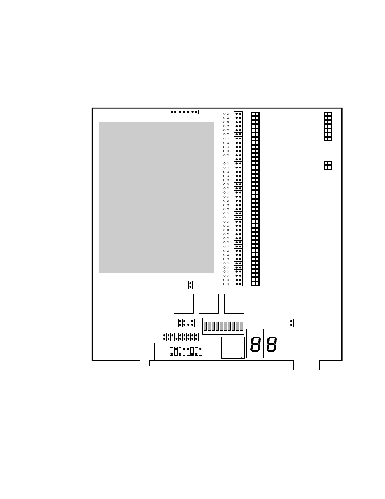
These resources are shown in the simplified view of the XStend Board (Figure 1). Each of
these resources will be described below.

6
them access to all the resources of the XStend Board. To use an XS40 Board with the
!!!
XStend Board, insert it into the right-most columns of the socket strips. When using an
XS95 Board, you should insert it into the left-most columns of the sockets. There are
markings on the XStend Board to indicate the appropriate column for each type of XS
Board.
If the XS Board is connected to a power supply through jack J9, then its power regulation
circuitry will supply VCC and GND to the XStend Board through the mounting sockets.
XS40 Boards with 3.3V FPGAs will supply both 3.3V and 5V to the XStend Board, while
XS40 Boards with 5V FPGAs and XS95 Boards will supply only 5V.
Warning: Version 1.0 of the XS40 Board with a 3.3V XC4000XL FPGA will not work
with the XStend Board because it supplies 3.3V but no 5V! You must replace the
XC4000XL FPGA with an XC4000E FPGA and remove the J8 jumper on the XS40
board to switch the board to 5V operation. Ignore this warning if you have Version
1.1 or higher.
External voltage supplies can also be used with the XStend Board. A 5V power supply
can be connected to header J12 and a 3.3V supply can be attached to header J14 as
shown in Figure 2. These supplies will power the attached XS Board as well as the
XStend electronics.
LEDs
• Figure 2: Connection of external power supplies to the XStend Board.
Warning: Do not attach external voltage supplies while also supplying power to the
XStend Board with an XS Board.
Warning: Never place shunts on either J12 or J14 or you will short the power
supplies to ground and damage the XStend Board and the attached XS Board..
The XStend Board provides a bargraph LED with eight LEDs (D1—D8) and two more
LED displays (U1 and U2) for use by an XS Board. All of these LEDs are active-low
meaning that an LED segment will glow when a logic-low is applied to it.
The LEDs are enabled and disabled by setting the shunts on the 2-pin jumpers as
described in Table 1.

7
• Table 1: Jumper settings for XStend LEDs.
JumperJumper SettingSetting
J8 Removing the shunt on this jumper disconnects the power from bargraph LEDs D1—D8. Placing the shunt on the
J4 Removing the shunt on this jumper disconnects the power from left LED digit U1. Placing the shunt on the jumper
J7 Removing the shunt on this jumper disconnects the power from right LED digit U2. Placing the shunt on the jumper
J13 A shunt placed on this jumper will enable the LEDs when you are using the XStend Board with an XS95 Board. This
jumper enables the bargraph LEDs.
enables the LED digit.
enables the LED digit.
shunt must be removed if you are using an XS40 Board with the XStend Board!!
Listing 1 and Listing 2 show the connections from the XS40 and XS95 Boards to the
LEDs on the XStend Board expressed as UCF constraints (for the UCF syntax and usage
tips, check out http://www.xilinx.com/techdocs/2449.htm).
• Listing 1: Connections between the XStend LEDs and the XS40.
# LEFT LED DIGIT SEGMENT CONNECTIONS (ACTIVE-LOW)
NET LSB<0> LOC=P3;
NET LSB<1> LOC=P4;
NET LSB<2> LOC=P5;
NET LSB<3> LOC=P78;
NET LSB<4> LOC=P79;
NET LSB<5> LOC=P82;
NET LSB<6> LOC=P83;
NET LDPB LOC=P84;
#
# RIGHT LED DIGIT SEGMENT CONNECTIONS (ACTIVE-LOW)
NET RSB<0> LOC=P59;
NET RSB<1> LOC=P57;
NET RSB<2> LOC=P51;
NET RSB<3> LOC=P56;
NET RSB<4> LOC=P50;
NET RSB<5> LOC=P58;
NET RSB<6> LOC=P60;
NET RDPB LOC=P28;
#
# INDIVIDUAL LED CONNECTIONS (ACTIVE-LOW)
NET DB<1> LOC=P41;
NET DB<2> LOC=P40;
NET DB<3> LOC=P39;
NET DB<4> LOC=P38;
NET DB<5> LOC=P35;
NET DB<6> LOC=P81;
NET DB<7> LOC=P80;
NET DB<8> LOC=P10;
• Listing 2: Connections between the XStend LEDs and the XS95.
# LEFT LED DIGIT SEGMENT CONNECTIONS (ACTIVE-LOW)
NET LSB<0> LOC=P1;

8
NET LSB<1> LOC=P2;
!!!!!!
NET LSB<2> LOC=P3;
NET LSB<3> LOC=P75;
NET LSB<4> LOC=P79;
NET LSB<5> LOC=P82;
NET LSB<6> LOC=P83;
NET LDPB LOC=P84;
#
# RIGHT LED DIGIT SEGMENT CONNECTIONS (ACTIVE-LOW)
NET RSB<0> LOC=P58;
NET RSB<1> LOC=P56;
NET RSB<2> LOC=P54;
NET RSB<3> LOC=P55;
NET RSB<4> LOC=P53;
NET RSB<5> LOC=P57;
NET RSB<6> LOC=P61;
NET RDPB LOC=P34;
#
# INDIVIDUAL LED CONNECTIONS (ACTIVE-LOW)
NET DB<1> LOC=P44;
NET DB<2> LOC=P43;
NET DB<3> LOC=P41;
NET DB<4> LOC=P40;
NET DB<5> LOC=P39;
NET DB<6> LOC=P37;
NET DB<7> LOC=P36;
NET DB<8> LOC=P35;
Switches
The XStend has a bank of eight DIP switches and two pushbuttons (labeled SPARE and
RESET) that are accessible from an XS Board. (There is a third pushbutton labeled
PROGRAM, which is used to initiate the programming of the XS40 Board. It is not
intended to be a general-purpose input.)
When closed or ON, each DIP switch pulls the connected pin of the XS Board to ground.
When the DIP switch is open or OFF, the pin is pulled high through a 10KΩ resistor.
When not being used, the DIP switches should be left in the open or OFF
configuration so the pins of the XS Board are not tied to ground and can freely
move between logic low and high levels.
When pressed, each pushbutton pulls the connected pin of the XS Board to ground.
Otherwise, the pin is pulled high through a 10 KΩ resistor.
Listing 3 and Listing 4 show the connections from the XS40 and XS95 Boards to the
switches on the XStend Board expressed as UCF constraints.
• Listing 3: Connections between the XStend DIP and pushbutton switches and the XS40.
# DIP SWITCH CONNECTIONS
NET DIPSW<1> LOC=P7;
NET DIPSW<2> LOC=P8;

9
NET DIPSW<3> LOC=P9;
NET DIPSW<4> LOC=P6;
NET DIPSW<5> LOC=P77;
NET DIPSW<6> LOC=P70;
NET DIPSW<7> LOC=P66;
NET DIPSW<8> LOC=P69;
#
# PUSHBUTTON SWITCH CONNECTIONS (ACTIVE-LOW)
NET SPAREB LOC=P67;
NET RESETB LOC=P37;
• Listing 4: Connections between the XStend DIP and pushbutton switches and the XS95.
# DIP SWITCH CONNECTIONS
NET DIPSW<1> LOC=P6;
NET DIPSW<2> LOC=P7;
NET DIPSW<3> LOC=P11;
NET DIPSW<4> LOC=P5;
NET DIPSW<5> LOC=P72;
NET DIPSW<6> LOC=P71;
NET DIPSW<7> LOC=P66;
NET DIPSW<8> LOC=P70;
#
# PUSHBUTTON SWITCH CONNECTIONS (ACTIVE-LOW)
NET SPAREB LOC=P67;
NET RESETB LOC=P10;
VGA Interface
The XStend Board provides an XS Board with an interface to a VGA monitor through
connector J5. (Version 1.2 and higher of the XS Boards already have their own VGA
interfaces, so the XStend circuitry is redundant for them.) The XS Board can drive the
active-low horizontal and vertical sync signals that control the width and height of the video
frame. The XS Board also has access to two bits each of red, green, and blue color
signals so it can generate pixels in any of 22×22×22=64 different colors.
Listing 5 and Listing 6 show the connections from the XS40 and XS95 Boards to the
VGA interface of the XStend Board. (These pin assignments are identical to the pin
assignments for the XS Boards, which have their own VGA interfaces.)
# VGA CONNECTIONS
NET VSYNCB LOC=P67;
NET HSYNCB LOC=P19;
NET RED<1> LOC=P18;
NET RED<0> LOC=P23;
NET GREEN<1> LOC=P20;
NET GREEN<0> LOC=P24;
NET BLUE<1> LOC=P26;
NET BLUE<0> LOC=P25;
• Listing 5: Connections between the XStend VGA interface and the XS40.

10
• Listing 6: Connections between the XStend VGA interface and the XS95.
# VGA CONNECTIONS
NET VSYNCB LOC=P24;
NET HSYNCB LOC=P15;
NET RED<1> LOC=P14;
NET RED<0> LOC=P18;
NET GREEN<1> LOC=P17;
NET GREEN<0> LOC=P19;
NET BLUE<1> LOC=P23;
NET BLUE<0> LOC=P21;
PS/2 Keyboard Interface
The XStend Board provides an XS Board with a PS/2-style interface (mini-DIN connector
J6) to either a keyboard or a mouse. The XS Board receives two signals from the PS/2
interface: a clock signal and a serial data stream that is synchronized with the falling edges
on the clock signal.
Listing 7 and Listing 8 show the connections from the XS40 and XS95 Boards to the
PS/2 interface of the XStend Board (expressed as UCF constraints):
• Listing 7: Connections between the XStend PS/2 interface and the XS40.
# PS/2 KEYBOARD CONNECTIONS
NET KB_CLK LOC=P68;
NET KB_DATA LOC=P69;
• Listing 8: Connections between the XStend PS/2 interface and the XS95.
# PS/2 KEYBOARD CONNECTIONS
NET KB_CLK LOC=P26;
NET KB_DATA LOC=P70;
RAMs
The XStend Board adds an additional 64 KBytes of RAM to the 32 KBytes already on the
XS Board. The XStend RAM connects to the same pins as the XS Board RAM for the
address bus, data bus, write-enable, and output-enable. The chip-selects of the XStend
Board RAMs are connected to different pins so all the RAMs can be individually selected.
Listing 9 and Listing 10 show the connections from the XS40 and XS95 Boards to their
own RAMs and the RAMs of the XStend Board (expressed as UCF constraints):
• Listing 9: Connections between the XStend RAMs and the XS40.
NET D<0> LOC=P41; # DATA BUS
NET D<1> LOC=P40;
NET D<2> LOC=P39;
NET D<3> LOC=P38;
NET D<4> LOC=P35;
NET D<5> LOC=P81;

11
NET D<6> LOC=P80;
NET D<7> LOC=P10;
NET A<0> LOC=P3; # LOWER BYTE OF ADDRESS
NET A<1> LOC=P4;
NET A<2> LOC=P5;
NET A<3> LOC=P78;
NET A<4> LOC=P79;
NET A<5> LOC=P82;
NET A<6> LOC=P83;
NET A<7> LOC=P84;
NET A<8> LOC=P59; # UPPER BYTE OF ADDRESS
NET A<9> LOC=P57;
NET A<10> LOC=P51;
NET A<11> LOC=P56;
NET A<12> LOC=P50;
NET A<13> LOC=P58;
NET A<14> LOC=P60;
NET WEB LOC=P62; # ACTIVE-LOW WRITE-ENABLE FOR ALL RAMS
NET OEB LOC=P61; # ACTIVE-LOW OUTPUT-ENABLE FOR ALL RAMS
NET CEB LOC=P65; # ACTIVE-LOW CHIP-ENABLE FOR XS40 RAM
NET LCEB LOC=P7; # ACTIVE-LOW CHIP-ENABLE FOR LEFT XSTEND RAM
NET RCEB LOC=P8; # ACTIVE-LOW CHIP-ENABLE FOR RIGHT XSTEND RAM
• Listing 10: Connections between the XStend RAMs and the XS95.
NET D<0> LOC=P44; # DATA BUS
NET D<1> LOC=P43;
NET D<2> LOC=P41;
NET D<3> LOC=P40;
NET D<4> LOC=P39;
NET D<5> LOC=P37;
NET D<6> LOC=P36;
NET D<7> LOC=P35;
NET A<0> LOC=P75; # LOWER BYTE OF ADDRESS
NET A<1> LOC=P79;
NET A<2> LOC=P82;
NET A<3> LOC=P84;
NET A<4> LOC=P1;
NET A<5> LOC=P3;
NET A<6> LOC=P83;
NET A<7> LOC=P2;
NET A<8> LOC=P58; # UPPER BYTE OF ADDRESS
NET A<9> LOC=P56;
NET A<10> LOC=P54;
NET A<11> LOC=P55;
NET A<12> LOC=P53;
NET A<13> LOC=P57;
NET A<14> LOC=P61;
NET WEB LOC=P63; # ACTIVE-LOW WRITE-ENABLE FOR ALL RAMS
NET OEB LOC=P62; # ACTIVE-LOW OUTPUT-ENABLE FOR ALL RAMS
NET CEB LOC=P65; # ACTIVE-LOW CHIP-ENABLE FOR XS95 RAM
NET LCEB LOC=P6; # ACTIVE-LOW CHIP-ENABLE FOR LEFT XSTEND RAM
NET RCEB LOC=P7; # ACTIVE-LOW CHIP-ENABLE FOR RIGHT XSTEND RAM

12
Stereo Codec
The XStend Board has a stereo codec that accepts two analog input channels from jack
J9, digitizes the analog values, and sends the digital values to the XS Board as a serial bit
stream. The codec also accepts a serial bit stream from the XS Board and converts it into
two analog output signals, which exit the XStend Board through jack J10.
The codec is configured by placing shunts on the jumpers as indicated in Table 2.
• Table 2: Jumper settings for XStend codec.
Jumper Setting
J11 Placing a shunt on this jumper disables the codec by holding it in the reset state. No shunt should be placed
J17 Removing this shunt prevents the codec’s serial data output from reaching the XS Board. A shunt should be
on this jumper when the codec is being used.
placed on this jumper when the codec is being used.
Listing 11 and Listing 12 show the connections from the XS40 Board to the codec
interface on the XStend Board (expressed as UCF constraints):
• Listing 11: Connections between the XStend stereo codec and the XS40 Board.
# STEREO CODEC CONNECTIONS
NET MCLK LOC=P9; # MASTER CLOCK TO CODEC
NET LRCK LOC=P66; # LEFT/RIGHT CODEC CHANNEL SELECT
NET SCLK LOC=P77; # SERIAL DATA CLOCK
NET SDOUT LOC=P6; # SERIAL DATA OUTPUT FROM CODEC
NET SDIN LOC=P70; # SERIAL DATA INPUT TO CODEC
NET CCLK LOC=P44; # CONTROL SIGNAL CLOCK
NET CDIN LOC=P45; # SERIAL CONTROL INPUT TO CODEC
NET CSB LOC=P46; # SERIAL CONTROL CHIP SELECT
• Listing 12: Connections between the XStend stereo codec and the XS95 Board.
# STEREO CODEC CONNECTIONS
NET MCLK LOC=P11; # MASTER CLOCK TO CODEC
NET LRCK LOC=P5; # LEFT/RIGHT CODEC CHANNEL SELECT
NET SCLK LOC=P72; # SERIAL DATA CLOCK
NET SDOUT LOC=P66; # SERIAL DATA OUTPUT FROM CODEC
NET SDIN LOC=P71; # SERIAL DATA INPUT TO CODEC
NET CCLK LOC=P46; # CONTROL SIGNAL CLOCK
NET CDIN LOC=P47; # SERIAL CONTROL INPUT TO CODEC
NET CSB LOC=P48; # SERIAL CONTROL CHIP SELECT
The analog stereo input and output signals enter and exit the XStend Board through the
1/8” jacks J9 and J10, respectively. The output of an audio CD player can be input
through J9 and a set of small stereo headphones can be connected to J10 for listening to
the processed output.
The digitized data output from the codec passes through jumper J17 on its way to the XS
Board inserted in the XStend Board. A shunt should be placed on J17 when the codec is
being used. Because the serial data output of the codec is not tristatable and because it

13
shares the input to the XS Board with other resources on the XStend Board, the shunt on
Xchecker Pin
XS40 Pin
1 – VCC (+5V)
2
2 – RT
32
3 – GND
52
4 – RD
30
6 – TRIG
7
7 – CCLK
73
9 – DONE
53
10 – TDI
15
11 – DIN
71
12 – TCK
16
13 – PROGRAM
55
14 – TMS
17
15 – INIT
41
16 – CLKI
13
17 – RST
8
18 – CLKO
9
J17 should be removed when the codec is not being used.
XILINX Xchecker Interface
An XS40 Board inserted in the XStend Board can be configured and tested using a
XILINX Xchecker cable attached to header J19. When using the Xchecker cable, you
must not connect the cable between the XS Board and the parallel port of the PC. In
addition, when using the Xchecker cable with an XStend/XS40 combination, you must
make the following adjustments to the XS40 Board:
n Remove the shunts from jumpers J4, J6, J10 and J11 of the XS40 Board;
n Remove the serial EPROM from socket U7.
The connections between the Xchecker cable and the XS40 Board is listed in Table 3.
• Table 3: Connections between the XStend Board Xchecker interface and the XS40 Board.
Prototyping Area
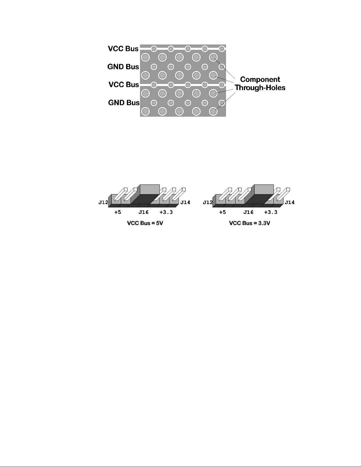
The XStend Board has a prototyping area consisting of component through-holes on an
0.1"×0.1" grid interspersed with a network of alternating VCC and GND buses as shown in
Figure 5. The buses carrying VCC run on the top side of the XStend Board while the GND
buses run on the bottom side. The VCC and GND buses have connection holes in which
a small wire can be soldered to make a connection to a nearby component through-hole.
14
• Figure 3: Top-side view of the network of VCC and GND buses around the component through-holes
in the XStend Board prototyping area.
The placement of the shunt on jumper J16 will determine whether the VCC buses in the
prototyping area carry either 5V or 3.3V (see Figure 6). Of course, the jumper selection
will have no effect unless you have both these voltages supplied to the XStend Board
either by the XS Board or by connecting external power supplies.
• Figure 4: Shunt placement for setting the VCC bus voltage..
Connections from the XS Board to the prototyping area are made through connector J3.
The arrangement of pins on this connector exactly matches the arrangement of pins on
the XS40 Board. For example, the pin at the bottom-left of J3 on the XStend Board
corresponds to pin 21 at the bottom-left of the XS40 Board.
The XS95 Board has a completely different pin arrangement than the XS40. Therefore,
each pin on J3 is explicitly labeled with the corresponding pin number on the XS95 Board.
For example, the pin at the bottom-left of J3 on the XStend Board is connected to pin 68
near the top-left of the XS95 Board.
Daughterboard Connector
Daughterboards with specialized circuitry can be connected to the XStend board through
connector J18. This 42×2 connector brings all the I/O and VCC/GND from the XS40 or
XS95 Board to the daughterboard.

Chapter
3
Programmer's Models
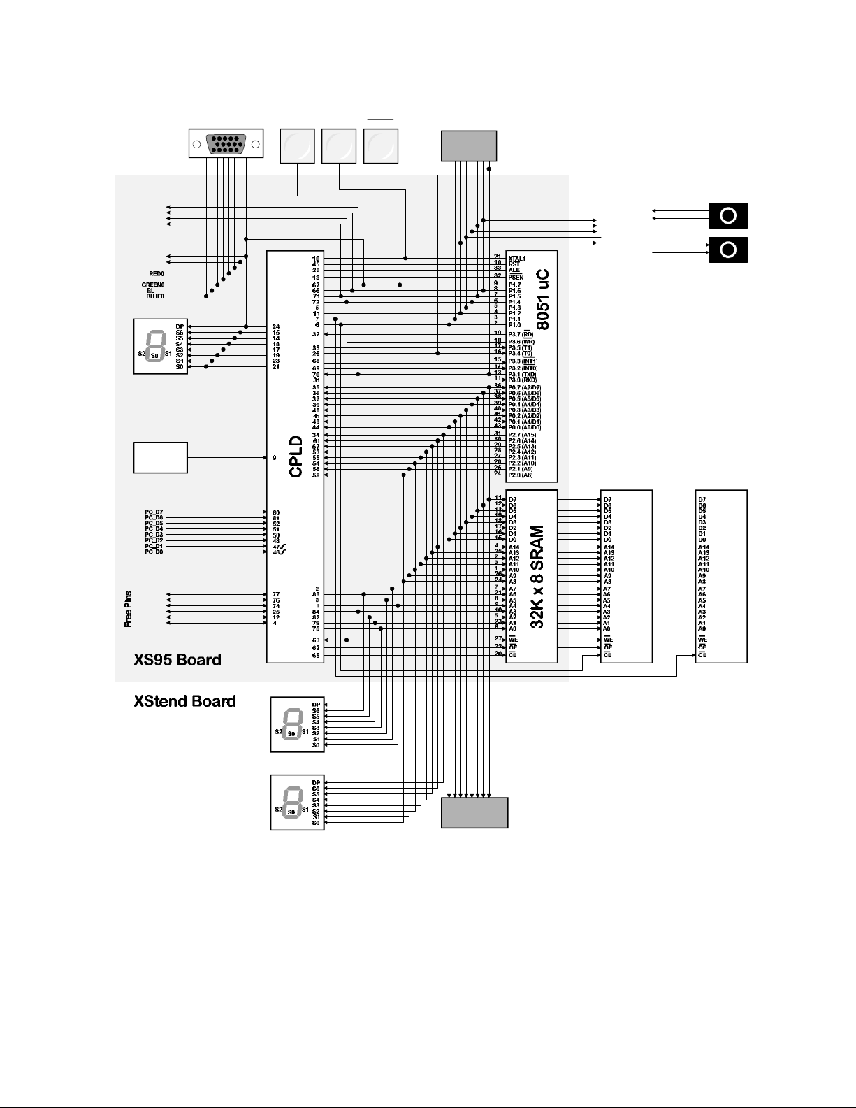
The interconnections of the XStend Board resources and an XS40 or XS95 Board are
shown in Figure 5 and Figure 6, respectively. These figures remove much of the
extraneous detail of the actual schematics, so we refer to them as programmer’s models.
Items within the shaded area in each figure correspond to circuitry housed on the XS
Board. The remaining items are XStend Board resources.
A cursory glance at the figures reveals that many of the resources share connections. For
example, the codec, DIP switch, and microcontroller port P1 are all connected to the same
set of pins on the FPGA or CPLD. So any design has to ensure that only one of these
resources is outputting data at any particular time. (Hence the need in some designs to
place the DIP switches in the OPEN position, or remove the shunt through which the
codec SDOUT drives serial data, or keep the microcontroller in the reset state.)
Table 4 and Table 5 list the same interconnection data for the XS40 and XS95 Boards,
respectively, in a tabular format, which makes it easier to see which resources share
common connections.

16
• Figure 5: Programmer's model of the XS40/XStend Board combination.
17

18
• Table 4: Connections between the XS40 Board and the XStend Board resources.
XS40 Pin
(J1,J3,J18)
PC Parallel
Port
UW-FPGA
BOARD Pin
2
+5V
+5V power source
3
LSB0A0Left LED segment; RAM address line
P354LSB1A1Left LED segment; RAM address line
P365LSB2A2Left LED segment; RAM address line
P296DIPSW4
SDOUT
P1.3
DIP switch; codec serial data output; uC I/O
P247DIPSW1
LCEB
P1.0
DIP switch; left RAM chip-enable, uC I/O port
P198DIPSW2
RCEB
P1.1
Power/ GND
DIP Switch
Push-buttons
LEDs
VGA
Interface
PS/2
Interface
RAMs
Stereo Codec
8051 uC
Oscillator
Function
•
 Loading...