

xrclS
.
.
.
XDL5SIGMA 2 COMPUTER
Xerox Data Systems
Reference Manual
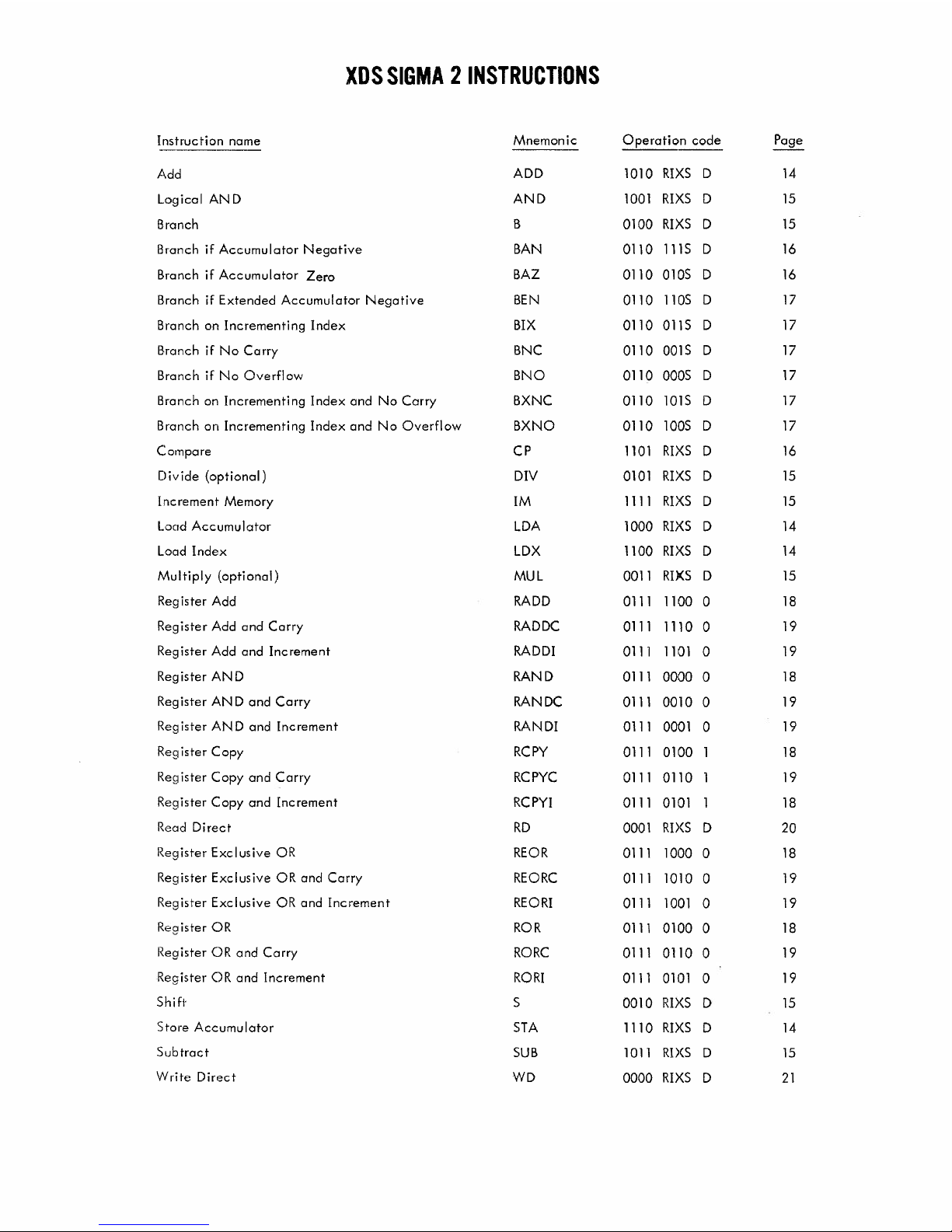
XDS SIGMA 2 INSTRUCTIONS
Instruction name
Mnemonic Operation code
Page
---------
Add
ADD
1010
RIXS D
14
Logical AND
AND 1001 RIXS D 15
Branch
B 0100 RIXS D 15
Branch if Accumulator Negative BAN
0110
ins
D 16
Branch if Accumulator Zero
BAZ
0110 010S D 16
Branch if Extended Accumulator Negative BEN
0110 lIDS D
17
Branch on Incrementing Index BIX 0110 OIlS D 17
Branch if No Carry BNC
0110 001S D 17
Branch if No Overflow BNO
0110
ODDS
D 17
Branch on Incrementing Index and No Carry BXNC
0110 101S
D 17
Branch on Incrementing Index and No Overflow
BXNO 0110 100S D 17
Compare CP
1101
RIXS
D 16
Divide (optional)
DIY 0101 RIXS D 15
Increment Memory
1M 1111 RIXS D 15
Load Accumulator LDA 1000 RIXS
D 14
Load Index
LDX 1100 RIXS D 14
Multiply (optional)
MUL 0011
RIXS D
15
Register Add
RADD 0111
1100
a
18
Register Add and Carry RADDC
0111 1110
a
19
Register Add and Increment RADD!
0111
1101
a
19
Register AND
RAND
0111 0000
0
18
Register AND and Carry
RAN DC
0111
0010
0
19
Reg ister AN D and Increment
RAND!
0111 0001
0
19
Reg ister Copy
RCPY
0111
0100
18
Register Copy and Carry
RCPYC
0111 0110 19
Register Copy and Increment
RCPYI
0111 0101 18
Read Direct
RD
0001
RD(S
D
20
Register Exclusive OR
REOR
0111 1000
a
18
Register Exclusive OR and Carry
REORC
0111
1010
a
19
Register Exclusive OR and Increment
REORI
0111 1001
0
19
Register OR
ROR
0111 0100
0
18
Register OR and Carry
RORC
0111
0110
0
19
Register OR and Increment
RORI
0111
0101
0
19
Shift
S
0010 RIXS D 15
Store AccumuIator
STA
1110
RIXS
D 14
Sub trac t
SUB
1011
RIXS
D 15
Write Direct
WD
0000
RIXS
D 21

Price: $2.00
XDS SIGMA 2 COMPUTER
REFERENCE MANUAL
900964F
December 1969
XJD:5
Xerox Data Systems/70l
South Aviation Boulevarcl/EI Segundo, California 90245
©
1966,1967,1966,1969,
Xerox Data Systems, Inc.
Printed in U.S.A.
REVISION
This publication, XDS 9009 64F, is a revision of the XDS Sigma 2 Computer Reference
Manual, XDS 9009 64E (dated May 1969). The primary revision is the addition of Appen-
dix D describing the Watchdog Timer. A change in text from that of the previous manual
is indicated by a vertical line in the margin of the page.
RELATED PUBLICATIONS
Title
XDS Sigma 2/3 Symbol Reference Manual
XDS Sigma 2/3 Extended Symbol Reference Manual
XDS Sigma 2/3 Basic FORTRAN/Basic FORTRAN IV Reference Manual
XDS Sigma 2 Mathematical Routines Technical Manual
XDS Sigma 2 Stand-Alone Systems Reference Manual
XDS Sigma 2/3 Basic Control Monitor Reference Manual
XDS Sigma 2/3 Real-Time Batch Monitor Reference Manual
XDS Sigma Interface Design Manual
ALL SPECIFICATIONS SUBJECT TO CHANGE WITHOUT NOTICE
ii
Publication No.
90 1051
90 1052
900967
90 1036
90 1047
90 1037
90 1037
900973
CONTENTS
1.
SYSTEM DESIGN FEATURES
SELECT
31
REGISTER
31
General Characteristi cs
2
MEMORY
31
Real-Time and Mul tiusage Features
3
INTERRUPT/INCREMENT ADDRESS
31
4
INITIALIZE
31
2. SYSTEM ORGANIZATION
COMPUTE
31
Information Format
4
Initial Loading Procedure
32
Core Memories
4
Central Processing Unit
5
Register Block
5
APPENDIXES
Arithmetic and Control Unit
5
Instruction Format
7
A. REFERENCE TABLES
33
Effective Address Computation
7
XDS Standard Symbols and Codes
33
Instruction Timing
8
XDS Standard Character Sets
33
Interrupt System
8
Control Codes
33
Internal Interrupt Levels
8
Special Code Properties
33
External Interrupt Levels
10
XDS Standard 8-Bit Computer Codes (EBCDIC) __
34
Interrupt Level States
10
XDS Standard 7-Bit Communication Codes
Interrupt System Control
11
(USASCII)
34
Interrupt Priority Sequence
12
Interrupt Routine Entry and Exit
12
XDS Standard Symbol-Code Correspondences--
35
Hexadecimal Arithmetic
39
Counter Interrupt Processing
12
Addition Table
39
CPU Interrupt Recognition
13
Multiplication Table
39
Protection System
13
Table of Powers of SixteenlO
40
3.
INSTRUCTION REPERTOIRE
14
Table of Powers of Ten16 40
Hexadecimal-Decimal Integer Conversion Toble.L;
41
Memory Reference Instructions
14
Hexadecimal-Decimal Fraction Conversion Toble.L
47
Conditional Branch Instructions
16
Table of Powers of Two
51
Copy Instruction
17
Mathematical Constants
51
Direct Control Instructions
19
B.
INSTRUCTION EXECUTION CYCLE
52
4. INPUT/OUTPUT OPERATIONS
22 C.
MEMORY ADDRESSING
54
Byte-Oriented I/O System
22
External Memory Adapter Model
54
Device Number
22 External Memory Adapter Model 2
54
I/o Control Doublewords
22 Conti nuous Addressing
54
Operational Status Byte
23
D.
WATCHDOG TIMER
Device Orders
24
55
I/O Tables
24
INDEX
56
Device Interrupts
25
I/O Instructions
25
ILLUSTRATIONS
Device Status Byte
26
External Interface System
27
Frontispiece - SIGMA 2 Computer System
iv
Direct-to-Memory Interface
28
1.
SIGMA 2 System Configuration
1
5.
OPERATOR CONTROLS
29
2.
SIGMA 2 Central Processing Unit_
6
3.
Interrupt Level Operation _____________
11
Control Panel
29
4.
Interrupt Priority Chain
12
POWER
29
5.
I/O Control Doublewords and I/o Tables _~ __
25
PHASE
29
6. SIGMA 2 Processor Control Pane
I
29
PROTECT PROGR
29
7.
SIGMA 2 Instruction Execution Diagram
53
INTERRUPT INHIBIT
29
O'FLOW
29
TABLES
CARRY
29
PARITY ERROR
30
1.
Effective Address Computation and Timing ____
8
PROTECT
30 2. Core Memory Allocation and Interrupt
PROG ADD
30 Priority Groupings ------ ---------- -- -
9
Key-Operated Switch 30 3.
READ DIRECT Internal Control Functions ___
20
DISPLAY
30
4.
WRITE DIRECT Internal Control
Functions ___
21
DATA
30
5.
Device Status Byte
27
iii

1. SYSTEM DESIGN FEATURES
SIGMA 2, a third-generation computer system, is a totally
integrated combination of high performance hardware and
efficient software. The SIGMA 2 system makes fuIIuse of
advanced design features first developed for SIGMA?, and
it provides the user with a balanced system that offers ad-
vantages normally found onl y in large computer systems.
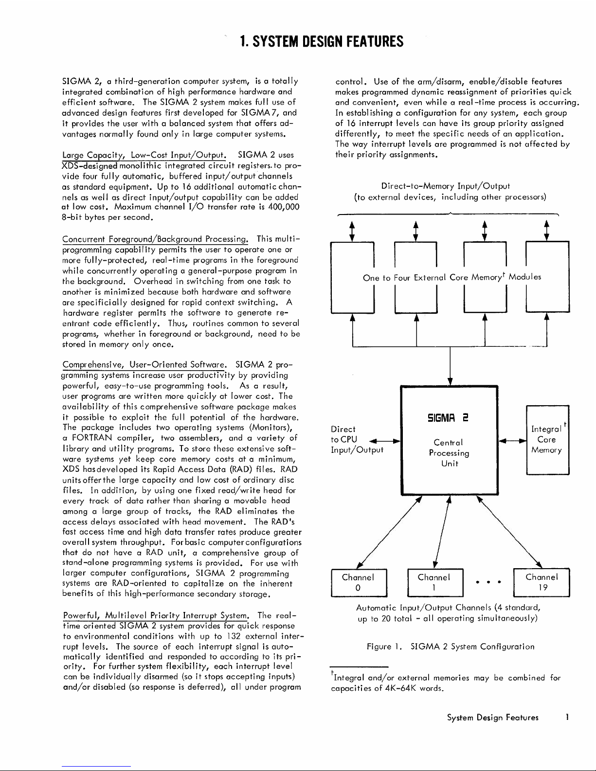
Large Capacity, Low-Cost Input/Output. SIGMA 2 uses
XDS-designed monolithic integrated circuit registers. to pro-
vide four fully automatic, buffered input/output channels
as standard equipment. Up to 16 additional automatic chan-
nels as well as direct input/output capability can be added
at low cost. Maximum channel I/O transfer rate is 400,000
8-bit bytes per second.
Concurrent Foreground/Background Processing. This multi-
programming capabiIity permits the user to operate one or
more fully-protected, real-time programs in the foreground
while concurrentIy operating a general-purpose program in
the background. Overhead in switching from one task to
another is minimized because both hardware and software
are specificially designed for rapid context switching. A
hardware register permits the software to generate re-
entrant code efficiently. Thus, routines common to several
programs, whether in foreground or background, need to be
stored in memory only once.
Comprehensive, User-Oriented Software. SIGMA 2 pro-
gramming systems increase user productivity by providing
powerful, easy-to-use programming tools. As a result,
user programs are written more quickly at lower cost. The
avai labi Iity of thi s comprehensive software package makes
it possible to exploit the full potential of the hardware.
The package includes two operating systems (Monitors),
a FORTRAN compiler, two assemblers, and a variety of
library and utility programs. To store these extensive soft-
ware systems yet keep core memory costs at a minimum,
XDS has developed its Rapid Access Data (RAD) fiIes. RAD
units offer the large capacity and low cost of ordinary disc
files. In addition, by using one fixed read/write head for
every track of data rather than sharing a movable head
among a large group of tracks, the RAD eliminates the
access delays associated with head movement. The RAD's
fast access time and high data transfer rates produce greater
overall system throughput. Forbasic computer configurations
that do not have a RAD unit, a comprehensive group of
stand-alone programming systems is provided. For use with
larger computer configurations, SIGMA 2 programming
systems are RAD-oriented to capitalize on the inherent
benefits of this high-performance secondary storage.
Powerful, Multilevel Priority Interrupt System. The real-
time oriented SIGMA 2 system provides for quick response
to environmental conditions with up to 132 external inter-
rupt levels. The source of each interrupt signal is auto-
matically identified and responded to according to its pri-
ority. For further system flexibility, each interrupt level
can be individually disarmed (so it stops accepting inputs)
and/or disabled (so response is deferred), all under program
control. Use of the arm/disarm, enable/disable features
makes programmed dynamic reassignment of priorities quick
and convenient, even while a real-time process is occurring.
In establishing a configuration for any system, each group
of 16 interrupt levels can have its group priority assigned
differently, to meet the specific needs of an application.
The way interrupt levels are programmed is not affected by
their priority assignments.
Direct-to-Memory Input/Output
(to external devices, including other processors)
One to Four External Core Memoryt Modules
U
Direct
toCPU
Input/Output
SIGMR 2
Central
Processing
Unit
t
Integra
I
Core
Memory
~lnnel
~
...
Channel
19
Automatic Input/Output Channels (4 standard,
up to 20 total - all operating simultaneously)
Figure 1. SIGMA 2 System Configuration
tIntegral and/or external memories may be combined for
capacities of 4K-64K words.
System Design Features

GENERAL CHARACTERISTICS
In its field, the SIGMA 2 computer is unique in its ability
to function efficiently in general-purpose, real-time, and
multiusage computing environments. The advanced features
and operating characteristics contributing to this capabi Iity
are:
• both word and byte organizotion of memory for maxi-
mum efficiency (words are 16 bits plus
pori+y)
bytes
are 8 bits.)
• 16 memory sizes available, 4096 to 65,536 words
• ability to connect to SIGMA 5 or SIGMA 7 memory
systems
• an extensive instruction set that facilitates efficient
programming; SIGMA 2 instruction characteristics
include:
•
only one word of storage required for each
instruction
•
two levels of indexing and indirect addressing may
be invoked individually or simultaneously
relative addressing (forward and backward)
•
• use of index register 2 as a base address register
• direct reference of up to 1024 addresses; 256
addresses beginning with location zero, 256
addresses beginning with the base address; 256
addresses beginning with the current instruction
location (relative forward), 256 addresses back-
ward from the current instruction (relative
backward)
• eight general-purpose registers to control program
operations; all are available to the program, providing:
• two hardware index registers for preindexing (base
address), post-indexing, or both (double indexing)
• hardware register for subroutine linkages
• double-precision accumulator
• program address register
•
zero register (for a source of zeros)
temporary storage register
•
• rapid context switching, to preserve computer environ-
ment when switching from one program to another, in-
cluding automatic status preservation on interrupt
• both word- and byte-oriented I/O systems, for maxi-
mum flexibil ity
• up to 20 fully automatic I/O channels operating simul-
taneously (4 channels are standard)
• I/O data chaining, for gather-read and scatter-write
operatians
• information transfer rate of approximately one million
words per second for each external memory interface
• direct input/output of a full word without the use of an
I/O channel (optional)
2 General CharacterisHcs
• a real-time priority interrupt system that features:
• 2 to 16 internal interrupt levels and up to 132
external interrupt levels that can be individually
armed, enabled and triggered by program control
• automatic identification, customer-designoted pri-
ority assignments, and extremely fast response time
• memory parity interrupt (optional)
• an optional power fail-safe feature, for automatic
and safe shutdown in the event of a power fai lure,
and unattended startup when power returns
• an optional system protection feature that incl udes
both memory write protection and operation pro-
tection for foreground programs
• up to four real-ti'me clocks (with a choice of reso-
lutions)for independent time bases, available as
an option
a comprehensive array of modular software that expands
in capability and speed as the system grows, with no
reprogramming required
•
• Free-standing software for small systems includes
Symbol and XDS Basic FORTRAN
• XDS Monitor for user convenience and increased
capability in large systems
• Symbol, a basic symbol ic assembler
• Extended Symbol for expanded features
• XDS Basic FORTRAN
• XDS FORTRAN IV
General Debug for symbol ic program
troubl eshooti ng
• Concordance program for documentation
•
• System Generation program for creating instal-
lation master
• Mathematics Library of standard functions
• Bootstrap Generator for producing self-loading
object programs
The wide range of standard and special-purpose peripheral
equipment, already proven in field operations, includes:
• Rapid-Access Data Files: Capacities for 750,000 to
24,000,000 bytes per control unit; transfer rate of
over 185,000 bytes/second; average access time of
17 milliseconds. Fixed read/write head per track
eliminates positioning time associated with movable-
arm storage devices
• Magnetic Tape Units: 9-track, IBM-compatible
60, 000 or 120, 000 bytes/second transfer rate; 7-track,
IBM-compatible, 15,000/20,000/41,700/60,000
characters/second transfer rates
• Paper Tape Readers and Punches: readers with speeds
of 20 and 300 characters/second, punches with speeds
of 10 and 120 characters/second, plus spoolers
• Keyboard Printers: available with or without a paper
tape reader and paper tape punch
• Card Readers: read cards punched in binary or EBCDIC
card code, 200 to 1500 cpm
• Card Punches: binary or EBCDIC card codes, 300 cpm
• Line Printers: fully buffered, with 132 print positions
and carriage control, 600 or 1000 Ipm
• Graph Plotter: for two-axis plotting of data under
digital control, 300 increments/second
• Display Equipment: oscilloscope display units, light
guns, and character and vector generators
• Data Communications Equipment: a complete line of
character- and message-oriented equipment
REAL-TIME AND MULTIUSAGE FEATURES
Real-time applications are characterized by a need for hard-
ware that provides quick response to an external environment,
sufficient speed to keep up with the real-time process itself,
and input/output flexibility to handle a wide variety of types
of data at varying speeds.
Multiusage applications, as implemented in SIGMA 2, are
defined as the combining of real-time and background pro-
cessing techniques into one system. The most difficult gen-
eral computing problem is the real-time application with its
requirements for extreme speed and capacity. Because the
SIGMA 2 system has been designed on a real-time base, it
is well qualified for the mixture of applications in a multi-
usage envi ronment. Many of its hardware featu res that
prove valuable for real-time applications are equally useful
in background processing, but in different ways.
The major features that make SIGMA 2 uniquely suitable
for both real-time and multiusage appl ications are described
in the following paragraphs.
Input/Output Facilities. Three distinct SIGMA 2 input/
output systems offer flexibil ity and capacity to meet the
needs of both real-time and general-purpose users: the
byte-oriented, the direct-to-CPU, and the direct-to-
memory I/O systems.
In the byte-oriented I/O system, each automatic I/O chan-
nel has its own high-speed registers and operates indepen-
dently without requiring attention from the program once it
has been started. Data is transferred one byte (8 bits) at
a time. For high-speed peripherals, bytes are assembled
into words in the I/O section and only one memory refer-
ence is made for two bytes. For slow-speed peripherals,
one reference is made for every byte, with a partial write
operation performed by the memory. All I/O channels
may operate concurrently and parity checking is performed
automatically.
The optional direct-to-CPU input/output system uses only
a single instruction to transfer a full 16-bit data word to
and from the A register. The same instruction that trans-
fers data also provides a 16-bit control field for external
control and selection, and accepts status information
returned from the external device to permit rapid sensing of
an external condition. The direct I/O system is generally
used for short bursts of asynchronous data transfers to avoid
tying up an automatic channel. Direct I/O is also useful
when data is to be accepted at medium to high speeds and
each input must be examined immediately when received.
The optional direct-to-memory input/output system provides
an additional memory bus to each of four external memories.
It is used for very high speed I/O transfers to and from
external devices or other processors. Transfers proceed at
full memory speed on a word-oriented basis, with overlap-
ping of multiple I/O and compute occurring automatically
when multiple memory modules are available.
Priority Interrupt System. In a multiusage environment,
many elements are operating asynchronously with respect to
each other. Thus, having a true priority interrupt system,
as the SIGMA 2 does, is especially important. With it the
computer system can respond quickly (and in proper order)
to the many demands made upon it, without the high over-
head cost of complicated programming, lengthy execution
time, and extensive storage allocations. Programs that deal
with interrupt signals from special equipment must sometimes
be checked out before the equipment is actually available.
To simulate special equipment, any external SIGMA 2 inter-
rupt level can be triggered by the CPU itself through execu-
tion of a single instruction.
Context Switching. When responding to a new set of
interrupt-initiated circumstances, a computer system must
preserve the current operating environment while it sets up
the new environment. In SIGMA 2, relevant information
about the current environment is retained as a 32-bit pro-
gram status doubleword (PSD). When an interrupt occurs,
the current PSD is automatically stored at an arbitrary loca-
tion in memory and the interrupt-servicing routine begins,
following the location into which the PSD is stored. At the
end of the interrupt-servicing routine, the PSD is restored
and the interrupt level cleared.
Protection System. Both real-time and background programs
can be run concurrently in a SIGMA 2 system because the
real-time program can be protected against alteration. The
optional protection feature guarantees that protected areas
of memory cannot -be written into by a program residing in
unprotected memory. The protection feature also prevents
the execution of unprotected instructions that could change
the I/O system or the protection system. The protection
pattern can be changed very rapidly.
Real-Time Clocks. In real-time systems, timing informa-
tion must be provided to cause certain operations to occur
at specific instants. Other timing information is also neces-
sary, such as elapsed time after a given event, or the cur-
rent time of day. SIGMA 2 provides up to four real-time
clocks, with varying degrees of resolution, to meet these
needs. These clocks also facilitate handling of separate
time bases and relative time priorities. Three of the clock
counters can be driven from commercial o, c , line frequency
(60 or 50 Hz), from 2- or 8-Hz oscillators, or from an ex-
ternal input; the first (operational) counter is driven by a
SOO-Hz source.
Real-Time and Multiusage Features 3
2. SYSTEM ORGANIZATION
INFORMATION FORMAT
The basic element of SIGMA 2 information is a 16-bit word
in which the bit positions are numbered from 0 through 15,
as follows:
A SIGMA 2 word can also be divided into two 8-bit parts
(called bytes) in which the bit positions of each byte are
numbered from 0 through 7, as follows:
Byte 0
Byte 1
12
31.c..5
6701231.567
Two SIGMA 2 words can be combined to form a 32-bit ele-
ment (called a doubleword) in which the bit positions are
numbered from 0 through 31, as follows:
Most significant word Least significant word
o
I 2 3 4 5 6 7 B 9 10 11 12 13 \•• 15 16 17 18 19 20 21 22 23 24 25 26 27 28 29 30 31
A doubleword is always referred to by the address of its
most significant
word,
Binary information in SIGMA 2 computers is generally
expressed in hexadecimal notation because four binary dig-
its of information can be expressed by a single hexadecimal
digit. Thus, a byte can be expressed with a string of 2
hexadecimal digits, a word with a string of 4 hexadecimal
digits, and a doubleword with a string of 8 hexadecimal
digits. The following table lists hexadecimal digits and
their binary and decimal equivalents.
Hexadecimal Binary Decimal
0 0000 0
1 0001 1
2
0010
2
3 001l 3
4
0100
4
5 0101 5
6 0110 6
7
0111 7
8
1000
8
9 1001 9
A
1010 10
B 1011
11
C
1100
12
D 1101 T3
E
1110 14
F 1111 15
In this reference manual, a hexadecimal number isdisplayed
as a string of hexadecimal digits surrounded by single quotes
and preceded by the letter "X". For example, the binary
number 01011010 is expressed in hexadecimal notation as
X'5A'. Hexadecimal numbers are generally used to denote
4 System.Organization
addresses and data values; however, there are many instan-
ces in which decimal numbers are more meaningful or are
customary. Because the SIGMA assembler systems perform
decimalJhexadecimal conversions, addresses and data
values may be expressed as decimal numbers.
In SIGMA 2, fixed-point data consists of a 15-bit integer
and a sign. Positive numbers are represented in true binary
form, with a sign of zero. Negative numbers are repre-
sented in two's complement form, with a sign of one. All
arithmetic operations assume that this format is used. Logi-
cal operations in SIGMA 2, on the other hand, assume that
a logical data word format, consisting of 16 bits without
sign, is used.
CORE MEMORIES
A SIGMA 2 computer can be equipped with either {or both}
oftwo different types of core memory: integral and external.
A magnetic core memory can be provided as an integral port
of the SIGMA 2 central processor configuration. This inte-
gral memory is available only to the SIGMA 2 central pro-
cessor, and it provides a portion of the total SIGMA 2
system memory. In order to implement the maximum mem-
ory capacity {64K words}, external memory is required in
addition to {or in place of} the integral memory.
The external memory provides independent access poths for
ather processors or special (customer designed) devices;
thus, the SIGMA 2 central processor may share common
storage with other SIGMA 2's, SIGMA 5's, SIGMA 7's,
special I/O processors, or other devices. By using two
SIGMA 7 memory modules (of 16K words each) the external
memory system may constitute a 64K SIGMA 2 memory
system. An external memory adaptor allows the SIGMA 2
computer to treat each 32-bit word of the SIGMA 7memory
system as two 16-bit words. Special registers allow the
programmer to establish a correspondence between any
4096-word portion of SIGMA 2 memory addresses and any
2048-word portion of SIGMA 5/7 memory addresses
(32-bit word).
If integral memory is included in the system that also has
external memory, the integral memory utilizes the lower-
numbered memory locations. For example, if a 16K integral
memory and 16K words of external memory are used, the
integral memory contains locations 0 through 16K-l and
the external memory contains locations 16K through 32K-1.
When the SIGMA 2 memory system is 64K words, the mem-
ory is "wrap-around", or "circular", where the next loca-
tion after 64K-l is location
O.
If a system has less then
64K words, any fetch operation from a nonexistent storage
location causes zeros to be fetched, in which case a
memory parity error also occurs. An attempt to store infor-
mation in a nonexistent storage location essentially results
in a "no operation".
See Appendix C for more information on memory addressing.
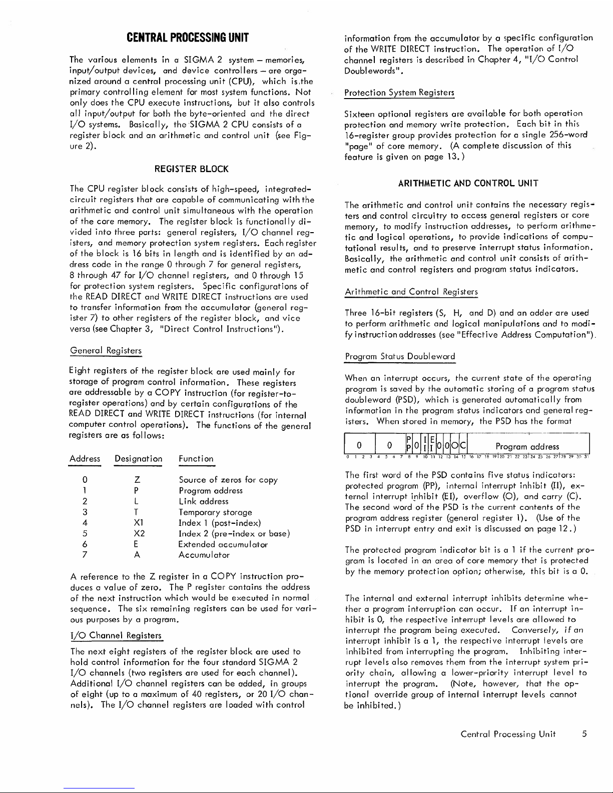
CENTRAL PROCESSING UNIT
The various elements in a SIGMA 2 system - memories,
input/output devices, and device controllers - are orga-
nized around a central processing unit (CPU), whichis.the
primary control Iing element for most system functions. Not
only does the CPU execute instructions, but it also controls
all input/output for both the byte-oriented and the direct
I/O systems. Basically, the SIGMA 2 CPU consists of a
register block and an arithmetic and control unit (see Fig-
ure 2).
REGISTER BLOCK
The CPU register block consists of high-speed, integrated-
circuit registers that are capable of communicating with the
arithmetic and control unit simultaneous with the operation
of the core memory. The register block is functionally di-
vided into three parts: general registers, I/o channel reg-
isters, and memory protection system registers. Each register
of the block is 16 bits in length and is identified by an ad-
dress code in the range 0 through 7 for general registers,
8 through 47 for I/O channel registers, and 0 through 15
for protection system registers. Specific configurations of
the READ DIRECTand WRITEDIRECTinstructions are used
to transfer information from the accumulator (general reg-
ister 7) to other registers of the register block, and vice
versa (see Chapter 3, "Direct Control Instructions").
General Registers
Eight registers of the register block are used mainly for
storage of program control information. These registers
are addressable by a COpy instruction (for register-to-
register operations) and by certain configurations of the
READ DIRECTand WRITEDIRECTinstructions (for internal
computer control operations). The functions of the general
registers are as follows:
Address Designation Functi on
0 Z
Source of zeros for copy
1
P
Program address
2
L Link address
3
T
Temporary storage
4
Xl
Index 1 (post-index)
5
X2 Index 2 (pre-index or base)
6
E Extended accumuIator
7 A Accumulator
A reference to the Z register in a COpy instruction pro-
duces a value of zero. The P register contains the address
of the next instruction which would be executed in normal
sequence. The six remaining registers can be used for vari-
ous purposes by a program.
I/O Channel Registers
The next eight registers of the register block are used to
hold control information for the four standard SIGMA 2
I/o channels (two registers are used for each channel).
Additional I/O channel registers can be added, in groups
of eight (up to a maximum of 40 registers, or 20 I/O chan-
nels). The I/O channel registers are loaded with control
information from the accumulator by a specific configuration
of the WRITEDIRECTinstruction. The operation of I/O
channel registers is described in Chapter 4, "I/O Control
Doublewords" .
Protection System Registers
Sixteen optional registers are available for both operation
protection and memory write protection. Each bit in this
16-register group provides protection for a single 256-word
"page" of core memory. (A complete discussion of this
feature is given on page 13.)
ARITHMETIC AND CONTROL UNIT
The arithmetic and control unit contains the necessary regis-
ters and control circuitry to access general registers or core
memory, to modify instruction addresses, to perform arithme-
tic and logical operations, to provide indications of compu-
tational results, and to preserve interrupt status information.
Basically, the arithmetic and control unit consists of arith-
metic and control registers and program status indicators.
Arithmeti c and Control Registers
Three 16-bit registers (S, H, and D) and an adder are used
to perform arithmetic and logical manipulations and to modi-
fy instruction addresses (see" Effective Address Computation").
Program Status Doubleword
When an interrupt occurs, the current state of the operating
program is saved by the automatic storing of a program status
doubleword (PSD), which is generated automatically from
information in the program status indicators and general reg-
isters. When stored in memory, the PSD has the format
The first word of the PSD contains five status indicators:
protected program (PP), internal interrupt inhibit (II), ex-
ternal interrupt i.!1hibit (EI), overflow
(0),
and carry (C).
The second word of the PSD is the current contents of the
program address register (general register 1). (Use of the
PSD in interrupt entry and exit is discussed on page 12.)
The protected program indicator bit is a 1 if the current pro-
gram is located in an area of core memory that is protected
by the memory protection option; otherwise, this bit is a
O.
The internal and external interrupt inhibits determine whe-
ther a program interruption can occur. If an interrupt in-
hibit is 0, the respective interrupt levels are allowed to
interrupt the program being executed. Conversely, if an
interrupt inhibit is a 1, the respective interrupt levels are
inhibited from interrupting the program. Inhibiting inter-
rupt levels also removes them from the interrupt system pri-
ority chain, allowing a lower-priority interrupt level to
interrupt the program. (Note, however, that the op-
tional override group of internal interrupt levels cannot
be inhibited.)
Central Processing Unit 5

REGISTER BLOCK
ARITHMETIC AND CONTROL UNIT
01
Zero
I
S
I
Memory Address
I
Arithmetic
lL
Program address
I
HI
Control
I
>
and control
registers
21
Link address
I
D
I
Memory Data
I
3L
Temporary storage
I
General
I
registers
0
41
Index 1
Protected program indicator
5 1
Index 2 (base)
I
D
Internal interrupt inhibit
I
D
Program
6
I
Extended accumul ator
External interrupt inhibit
status
indicators
7
I
Accumulator
I
D
Overflow indicator
0
Carry indicator
8L
Channel 0
I
<III
To/from
9L
Channel 0
I
core memory
·
Standard
·
I/O channel
I
Channel
3
I
registers
14
To/from
~
byte I/o system
15 [
Channel
3
I
I
..
READDIRECT
16
I
Channel 4
I
I
17
I
Channel 4
I
WRITEDIRECT
Optional
·
I/O channel
-
·
I
461
Channel
19
I
registers
~
Interrupts
Priority interrupt system
..•
471
Channel 19
1
I
o
~ddresses 0 through 4K-l
Protection
1
fAddresses 4K through 8K-l
I
>
system
·
regi sters
·
(optional)
·
ISIAddresses 60K through 64K-11
Figure 2. SIGMA 2 Central Processing Unit
6 Central Processing Unit
The overflow and carry indicators reflect the results of
various operations. The overflow indicator is set to 1 if
overflow occurs during an arithmetic operation. If, after
an arithmetic operation, there is a carry from the most sig-
nificant position (the sign' position) of the adder, the carry
indicator is set to
1.
This feature is useful in multiple-
precision operations, where the entire 16 bits are considered
to be the low-order part of an extended operation. Also,
on a subtract operation, the carry indicator will be set to
1 if there is a "borrow" from the sign position of the adder.
In arithmetic operations, the carry and overflow indicators
operate as described above. Some instructions, however,
use these indicators to record status information generated
as a resul t of the operation.
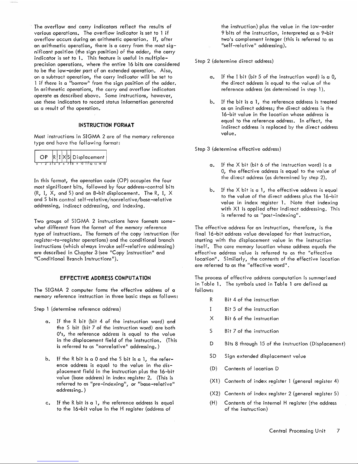
INSTRUCTION FORMAT
Most instructions in SIGMA 2 are of the memory reference
type and have the following format:
In this format, the operorion code (OP) occupies the four
most significant bits, followed by four address-control bits
(R, I, X, and S) and an 8-bit displacement. The R, I, X
and S bits control self-relative/nonrelative/base-relative
addressing, indirect addressing, and indexing.
Two groups of SIGMA 2 instructions have formats some-
what different from the format of the memory reference
type of instructions. The formats of the copy instruction (for
register-to-register operations) and the conditional branch
instructions (which always invoke self-relative addressing)
are described in Chapter 3 (see "Copy Instruction" and
"Conditional Branch Instructions").
EFFECTIVE ADDRESS COMPUTATION
The SIGMA 2 computer forms the effective address of a
memory reference instruction in three basic steps as follows:
Step 1 (determine reference address)
a. If the R bit (bit 4 of the instruction word) and
the S bit (bit 7 of the instruction word) are both
O's, the reference address is equal to the val ue
in the displacement field of the instruction. (This
is referred to as "nonrelative" addressing.)
b. If the R bit is a 0 and the S bit is a 1, the refer-
ence address is equal to the val ue in the dis-
placement field in the instruction plus the 16-bit
value (base address) in index register 2. (This is
referred to as "pre-indexing", or "base-relative"
addressing. )
c. If the R bit is a 1, the reference address is equal
to the 16-bit value in the H register (address of
the instruction) plus the value in the low-order
9 bits of the instruction, interpreted as a 9-bit
two's complement integer (this is referred to as
"self-relative" addressing).
Step 2 (determine direct address)
a. If the I bit (bit 5 of the instruction word) is a 0,
the direct address is equal to the value of the
reference address (as determined in step 1).
b. If the bit is a 1, the reference address is treated
as an indirect address; the direct address is the
16-bit value in the location whose address is
equal to the reference address. In effect, the
indirect address is replaced by the direct address
value.
Step 3 (determine effective address)
a. If the X bit (bit 6 of the instruction word) is a
0, the effective address is equal to the val ue of
the direct address (as determined by step 2).
b. If the X bit is a 1, the effective address is equal
to the value of the direct address plus the 16-bit
value in index register 1. Note that indexing
withXlis applied after indirect addressing. This
is referred to as "post-indexing".
The effective address for an instruction, therefore, is the
final 16-bit address value developed for that instruction,
starting with the displacement value in the instruction
itself. The core memory location whose address equals the
effective address value is referred to as the "effective
location". Similarly, the contents of the effective location
are referred to as the "effective word".
The process of effective address computation is summarized
in Table 1. The symbols used in Table 1 are defined as
follows:
R Bit 4 of the instruction
Bit 5 of the instruction
X Bit 6 of the instruction
S
Bit 7 of the instruction
D
Bits 8 through 15 of the instructian (Displacement)
SD Sign extended displacement value
(D) Contents of location D
(Xl)
Contents of index register 1 (general register 4)
(X2) Contents of index register 2 (general register 5)
(H) Contents of the internal H register (the address
of the instruction)
Central Processing Unit 7
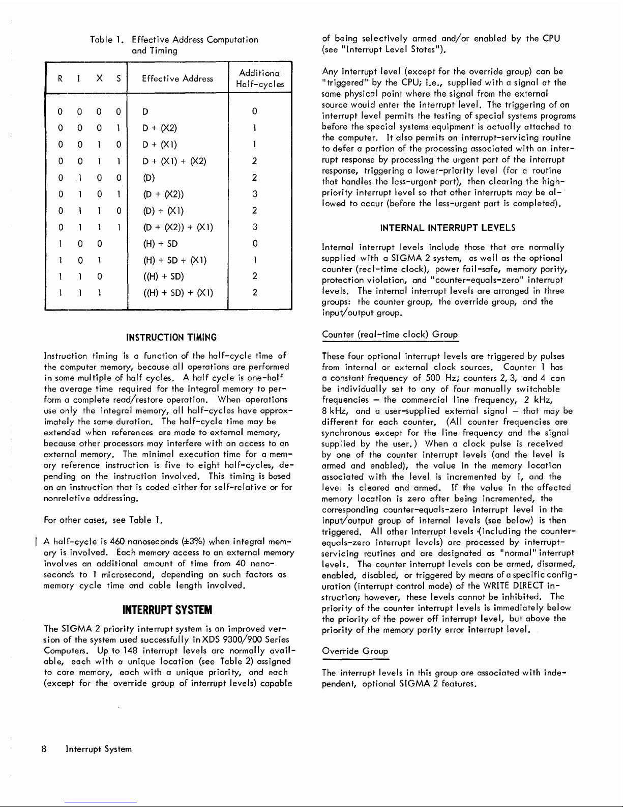
Table 1. Effective Address Computation
and Timing
R I
X
5
Effective Address
Additional
HaIf-cyc Ies
_.
0
0 0 0
D
0
0 0 0
1
D+ (X2)
1
0 0
1
0
D + (Xl)
1
0
0
1 1
D + (Xl) + (X2) 2
0
1
0 0
(D) 2
0
1
0
1
(D + (X2))
3
0
1 1
0
(D) + (Xl) 2
0
1
1
1
(D + (X2)) + (Xl)
3
1
0 0
(H) + SD 0
1
0
1
(H) + SD + (Xl)
1
1
1
0 «H) + SD)
2
1 1 1
«H) + SD) + (Xl)
2
'---.
INSTRUCTION TIMING
Instruction timing is a function of the half-cycle time of
the computer memory, because all operations are performed
in some multiple of half cycles. A half cycle is one-half
the average time required for the integral memory to per-
form a complete read/restore operation. When operations
use only the integral memory, all half-cycles have approx-
imately the same duration. The half-cycle time may be
extended when references ore made to external memory,
because other processors may interfere with an access to an
external memory. The minimal execution time for a mem-
ory reference instruction is five to eight half-cycles, de-
pending on the instruction involved. This timing is based
on an instruction that is coded either for self-relative or for
nonrelative addressing.
For other cases, see Table 1.
A half-cycle is 460 nanoseconds (±3%) when integral mem-
ory is involved. Each memory access to an external memory
involves an additional amount of time from 40 nano-
seconds to 1 microsecond, depending on such factors as
memory cycle time and cable length involved.
INTERRUPT SYSTEM
The SIGMA 2 priority interrupt system is an improved ver-
sion of the system used successfully inXDS 9300/900 Series
Computers. Up to 148 interrupt levels are normally avail-
able, each with a unique location (see Table 2) assigned
to core memory, each with a unique priority, and each
(except for the override group of interrupt levels) capable
8 Interrupt System
of being selectively armed and/or enabled by the CPU
(see "Interrupt Level States").
Any interrupt level (except for the override group) can be
"triggered" by the CPU; i.e., supplied with a signal at the
same physical point where the signal from the external
source would enter the interrupt level. The triggering of an
interrupt level permits the testing of special systems programs
before the special systems equipment is actually attached to
the computer. It also permits an interrupt-servicing routine
to defer a portion of the processing associated with an inter-
rupt response by processing the urgent part of the interrupt
response, triggering a lower-priority level (for a routine
that handles the less-urgent part), then clearing the high-
priority interrupt level so that other interrupts may be al-
lowed to occur (before the less-urgent part is completed).
INTERNAL INTERRUPT LEVELS
Internal interrupt levels include those that are normally
supplied with a SIGMA 2 system, as well as the optional
counter (real-time clock), power fail-safe, memory parity,
protection violation, and "counter-equals-zero" interrupt
levels. The internal interrupt levels are arranged in three
groups: the counter group, the override group, and the
input/output group.
Counter (real-time clock) Group
These four optional interrupt levels are triggered by pulses
from internal or external clock sources. Counter 1 has
a constant frequency of 500 Hz; counters 2, 3, and 4 can
be individually set to any of four manually switchable
frequencies - the commercial Iine frequency, 2 kHz,
8 kHz, and a user-supplied external signal - that may be
different for each counter. (All counter frequencies are
synchronous except for the Iine frequency and the signal
supplied by the user.) When a clock pulse is received
by one of the counter interrupt levels (and the level is
armed and enabled), the value in the memory location
associated with the level is incremented by 1, and the
level is cleared and armed. If the value in the affected
memory location is zero after being incremented, the
corresponding counter-equals-zero interrupt level in the
input/output group of internal levels (see below) is then
triggered. All other interrupt levels .(including the counter-
equals-zero interrupt levels) are processed by interrupt-
servicing routines and are designated as "normal" interrupt
levels. The counter interrupt levels can be armed, disarmed,
enabled, disabled, or triggered by means of a specific config-
uration (interrupt control mode) of the WRITEDIRECTin-
struction; however, these levels cannot be inhibited. The
priority of the counter interrupt levels is immediately below
the priority of the power off interrupt level, but above the
priority of the memory parity error interrupt level.
Override Group
The interrupt levels in this group are associated with inde-
pendent, optional SIGMA 2 features.
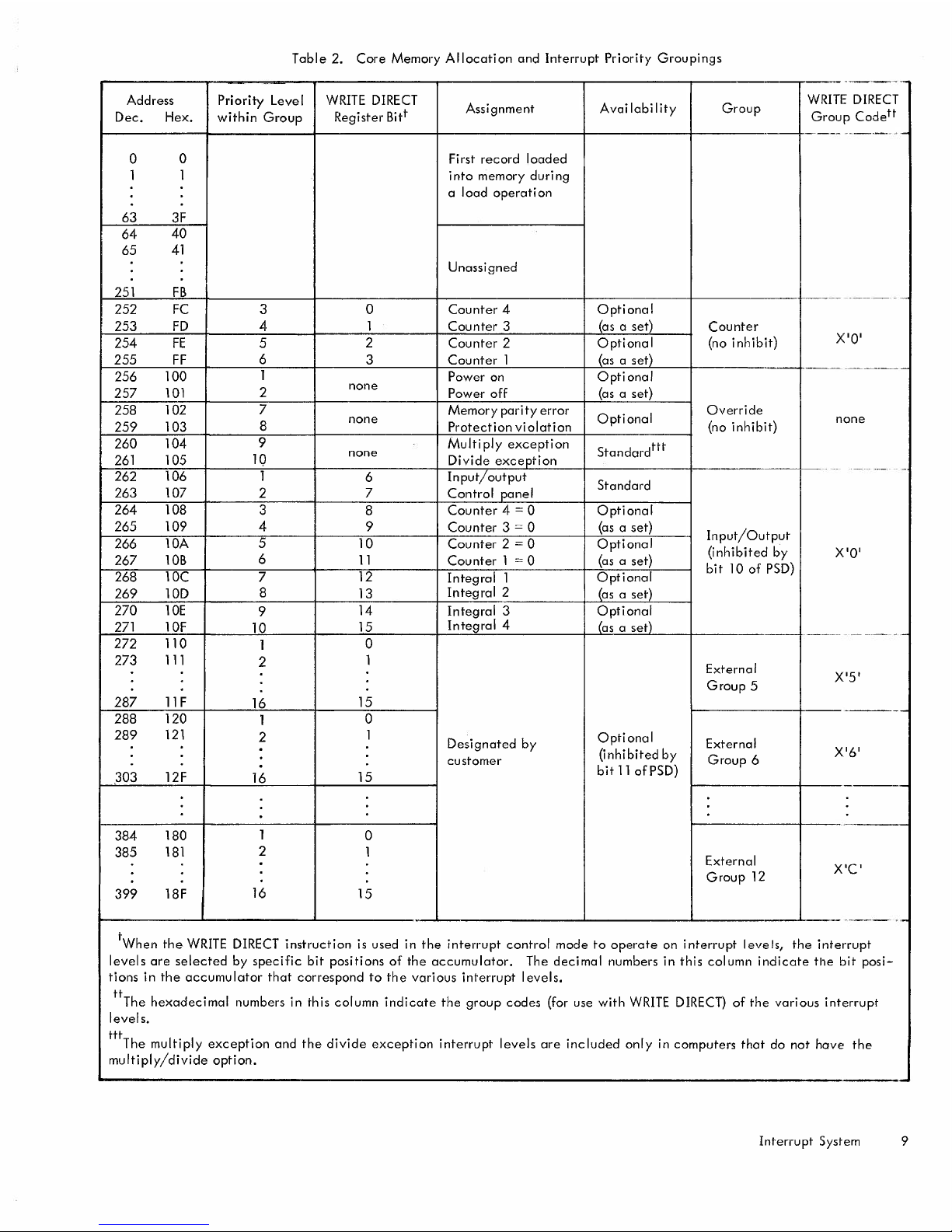
Table 2. Core Memory Allocation and Interrupt Priority Groupings
--
-~-.~---~
Address Priority Level WRITEDIRECT
Assignment
Avai labiIity Group
WRITEDIRECT
Dec. Hex. within Group
Register Bitt
Group Codett
---
---,-
...
---.
,-
0 0
First record loaded
1 1 into memory duri ng
a load operati on
63 3F
64
40
65
41
Unassigned
251 FB
-----
-_------
252 Fe 3 0
Counter 4 Optional
253 FD 4
1 Counter 3 (as a set)
Counter
254 FE
5
2
Counter 2
Optional
(no inhibit)
X'O'
255 FF
6
3 Counter 1
(as a set)
256 100
1
Power on Optional
--_
----------
257
101
2
none
Power off
(as a set)
258
102
7
Memory parity error
Optional
Override
259 103
8
none
Protection violation
(no inhibit)
none
260
104
9
Multiply exception
Standardttt
261 105 10
none
Divide exception
262
106 1
Input/output
-
,~-
-
6
Standard
263 107
2
7
Control panel
264 108
3
8
Counter 4==0 Optional
265 109 4 9
Counter 3==0
(as a set)
Input/Output
266
lOA
5
10
Counter 2==0 Optional
267
lOB
6
11
Counter 1==0
(as a set)
(inhibited by
X'O'
268 10C
7
12
Integral 1
Optional
bit 10 of PSD)
269 10D
8
13
Integral 2
(as a set)
270 10E
9
14
Integral 3
Optional
271 10F
10
15
Integral 4
(as a set)
--
-~----
-----_.-
272 110
1
0
273
111
2
1
External
Group 5
X'5'
287 11F
16
15
288
120
0
------
1
289 121
2
1
Designated by
Optional
External
·
(inhibited by
X'6'
·
customer
bit 11 of PSD)
Group 6
303
12F
16
15
--
384
180
1
0
385
181
2
1
External
·
X'C'
Group 12
399 18F
16
15
.
----_
..
-
,_
tWhen the WRITEDIRECTinstruction is used in the interrupt control mode to operate on interrupt levels, the interrupt
levels are selected by specific bit positions of the accumulator.
The decimal numbers in this column indicate the bit posi-
tions in the accumulator that correspond to the various interrupt levels.
ttThe hexadecimal numbers in this column indicate the group codes (for use with WRITEDIRECT)of the various interrupt
levels.
tttThe multiply exception and the divide exception interrupt levels are included only in computers that do not have
the
multiply/divide option.
Interrupt System 9
The override interrupt levels are always armed (cannot be
disarmed), always enabled (cannot be disabled), cannot be
triggered by a WRITE DIRECT instruction, and cannot be
inhibited.
Power Fail-Safe. The two optional power fail-safe inter-
rupt levels are used to enter routines that save and restore
volati Ie information in the event of a power fai lure. The
power-off interrupt level is triggered whenever the power
supply voltage falls below a safe limit; likewise, the power-
on interrupt level is triggered whenever power returns to
safe limits. The power fail-safe interrupt levels have a
higher-priority than the counter interrupt levels.
Memory Parity Error. The memory parity interrupt option
is used to inform the program (or the computer operator) that
a parity error has occurred upon accessing memory for an
instruction, direct address (in the case of indirect address-
ing), or an operand. If the option is installed and the
PARITY ERROR switches on the control panel are in the
INTERRUPT/NORMAL positions when a parity error occurs,
the memory parity interrupt level is triggered.
Protection Violation. The protection option includes the
protection violation interrupt level. (The protection option
is described on page 13.) If the option is installed and the
PROTECT switch on the processor control panel is in the ON
position when a protection violation is encountered, the
protection violation interrupt level is triggered.
Multiply/Divide Exception. The multiply/divide option
includes the additional logic required for executing the
MULTIPLY and DIVIDE instructions. If the option is not
installed, the multiply exception interrupt level and the
divide exception interrupt levels are provided to allow for
simulation of the unimplemented instructions. In this case,
the appropriate exception interrupt level is triggered, when-
ever an attempt is made to execute a MULTIPLY or DIVIDE
instructi on.
Input/Output Group
This interrupt group includes two standard interrupt levels
and eight optional levels. The I/O and control panel in-
terrupt levels are standard; the four counter-equals-zero
interrupt levels and the four integral interrupt levels are
optional.
All interrupt levels in the input/output group can be in-
hibited by means of the internal interrupt inhibit (bit 10
of the PSD), and can be armed, disarmed, enabled, dis-
abled, and triggered by specific configurations of the
WRITE DIRECT instruction.
I/O Interrupt Level. The I/O interrupt level accepts in-
terrupt signals from the standard I/o system. An I/O rou-
tine must contain an ACKNOWLEDGE I/o INTERRUPT
(AIO) instruction that identifies the source and cause of
an I/O interrupt.
Control Panel Interrupt Level. The control panel interrupt
level is connected to the INTERRUPT switch on the proces-
sor control panel. The control panel interrupt level can
10 Interrupt System
thus be triggered by the computer operator, allowing him to
initiate a specific routine.
Counter-equals-zero Interrupt Levels. The counter-equals-
zero interrupt levels are associated with the four optional
real-time clocks. For each clock option installed, the CPU
automatically increments one of four core memory {counter}
locations as the clock pulses are received. When the value
in a counter location equals zero, the corresponding counter-
equals-zero interrupt level is triggered. Counting continues
after the interrupt level is triggered; unless the counter in-
terrupt level is disarmed or disabled, counting will continue
until zero is reached again. (See "Counter Interrupt Pro-
cessing". )
EXTERNAL INTERRUPT LEVELS
A SIGMA 2 system can contain up to 9 groups of optional
interrupt levels, with up to 4 levels in the first integral
group and up to 16 levels in each of the 8 external groups.
The integral levels are controlled as part of the input/
output group of internal interrupt levels (i. e., inhibited
with the internal interrupt inhibit), and have a lower pri-
ority than the other levels in the input/output group. All
interrupts are controlled separately (i.e., inhibited with the
external interrupt inhibit), and can be arranged in almost
any priority sequence (see "Interrupt Priority Sequenc.e").
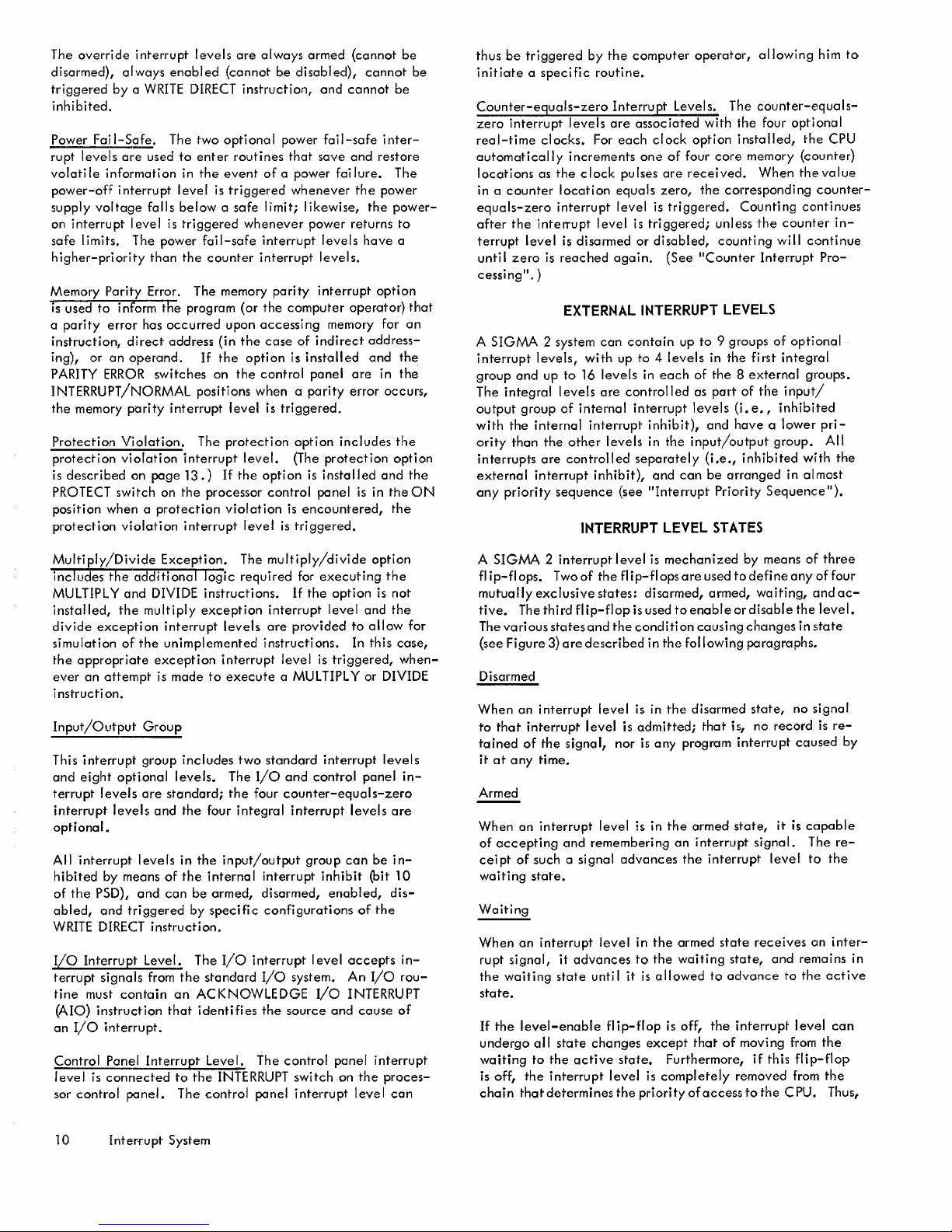
INTERRUPT LEVEL STATES
A SIGMA 2 interrupt level is mechanized by means of three
flip-flops. Twoof the flip-fl opsare used to define any offour
mutually exclusive states: disarmed, armed, waiting, and ac-
tive. Thethird fl
lp-Flop
is used to enabl e or disable the level.
Thevarious states and the condition causing changes in state
(see Figure 3) are described in the following paragraphs.
Disarmed
When an interrupt level is in the disarmed state, no signal
to that interrupt level is admitted; that is, no record is re-
tained of the signal, nor is any program interrupt caused by
it at any time.
Armed
When an interrupt level is in the armed state, it is capable
of accepting and remembering an interrupt signal. The re-
ceipt of such a signal advances the interrupt level to the
waiting state.
Waiting
When an interrupt level in the armed state receives an inter-
rupt signal, it advances to the waiting state, and remains in
the waiting state until it is allowed to advance to the active
state.
If the level-enable flip-flop is off, the interrupt level can
undergo all state changes except that of moving from the
waiting to the active state. Furthermore, if this flip-flop
is off, the interrupt level is completely removed from the
chain that determines the priority of access to the C PU. Thus,
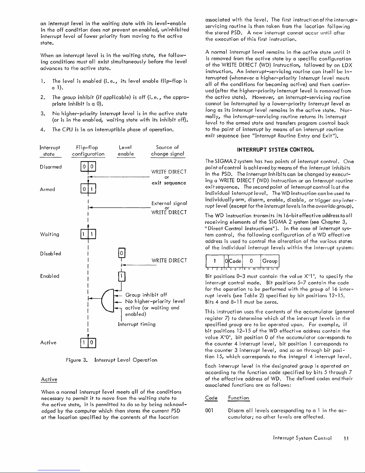
an interrupt level in the waiting state with its level-enable
in the off condition does not prevent an enabled, uninhibited
interrupt level of lower priority from moving to the active
state.
When an interrupt level is in the waiting state, the follow-
ing conditions must all exist simultaneously before the level
advances to the active state.
1. The level is enabled (i. e., its level enable fl ip-flop is
a
I).
2. The group inhibit (if applicable) is off (i. e., the appro-
priate inhibit is a OJ.
3. No higher-priority interrupt level is in the active state
(or is in the enabled, waiting state with its inhibit off).
4.
The CPU is in an interruptible phase of operation.
Interrupt
state
Flip-flop
configurati on
Source of
change signal
Level
enable
Disarmed
WRITEDIRECT
ar
exit sequence
Armed
External signal
~------------------ or
WRITEDIRECT
Waiting
I
I
$
Disabled
WRITEDIRECT
Enabled
Active
I
I
I
I
I
~
Group inhibit off
No higher-priority level
active (or waiting and
enabled)
Interrupt timing
Figure 3. Interrupt Level Operation
Active
When a normal interrupt level meets all of the conditions
necessary to permit it to move from the waiting state to
the active state, it is permitted to do so by being acknowl-
edged by the computer which then stores the current PSD
at the location specified by the contents of the location
associated with the level. The first instruction of the interrupt-
servicing routine is then taken from the location following
the stored PSD. A new interrupt cannot occur untiIafter
the execution of this first instruction.
A normal interrupt level remains in the active state until it
is removed from the active state by a specific configuration
of the WRITEDIRECT(WD) instruction, followed by an LDX
instruction. An interrupt-servicing routine can itself be in-
terrupted (whenever a higher-priority interrupt level meets
all of the conditions for becoming active) and then contin-
ued (after the higher-priority interrupt level is removed from
the active state). However, an interrupt-servicing routine
cannot be interrupted by a lower-priority interrupt level as
long as its interrupt level remains in the active state. Nor-
mally, the interrupt-servicing routine returns its interrupt
level to the armed state and transfers program control back
to the point of interrupt by means of an interrupt routine
exit sequence (see "Interrupt Routine Entry and Exit").
INTERRUPT SYSTEM CONTROL
The SIGMA 2 system has two points of interrupt control. One
point of control isachieved by meansof the interrupt inhibits
in the PSD. Theinterruptinhibitscan be changed byexecut-
ing a WRITEDIRECT(WD) instruction or an interrupt routine
exit sequence. The second point of interrupt control isatthe
individua I interrupt level. The WD instruction can be used to
individually arm, disarm, enable, disable, or trigger any inter-
rupt level (except for the interrupt levels in the override group).
The WD instruction transmits its 16-biteffective address toall
receiving elements of the SIGMA 2 system (see Chapter 3,
"Direct Control Instructions"). In the case of interrupt sys-
tem control, the following configuration of a WD effective
address is used to control the alteration of the various states
of the individual interrupt levels within the interrupt system:
Bit positions 0-3 must contain the value X'I', to specify the
interrupt control mode. Bit positions 5-7 contain the code
for the operation to be performed with the group of 16 inter-
rupt levels (see Table 2) specified by bit positions 12-15.
Bits 4 and 8-11 must be zeros.
Thi5instructi on uses the contents of the accumu Iator (general
register 7) to determine which of the interrupt levels in the
specified group are to be operated upon. For example, if
bit positions 12-15 of the WD effective address contain the
value X'O', bit position 0 of the accumulator corresponds to
the counter 4 interrupt level, bit position 1 corresponds to
the counter 3 interrupt level, and so on through bit posi-
tion 15, which corresponds to the integral 4 interrupt level.
Each interrupt level in the designated group is operated on
according to the function code specified by bits 5 through 7
of the effective address of WD. The defined codes and their
associated functions are as follows:
Code
Functi on
001
Disarm all levels corresponding to a 1 in the ac-
cumulator; no other levels are affected.
Interrupt System Control 11

Code Function
010
Arm and enable all levels corresponding to a 1 in
the accumulator; no other levels are affected.
Arm and disable all levels corresponding to
CI
1 in
the accumulator; no other levels are affected.
Enable all levels corresponding to a 1 in the ac-
cumulator; no other levels are affected.
Disable all levels corresponding to a 1 in the ac-
cumulator; no other levels are affected.
110 Enable all levels corresponding to a 1 in the ac-
cumulator and disable all other levels.
011
100
101
Trigger
011
levels corresponding to a 1 in the ac-
cumulator. All such levels that are currently
armed advance to the waiting state. Those levels
currently disarmed are not altered, and all levels
corresponding to a 0 in the accumulator are not
affected. The interrupt trigger is applied at the
same input point as that used by the device con-
nected to the interrupt level.
The recommended method for produc ing the appropriate con-
figuration of the WRITEDIRECTeffective address is to indi-
rectly address a memory location that contains the appro-
priate bit configuration for the desired effective address.
111
INTERRUPT PRIORITY SEQUENCE
SIGMA 2 interrupts are arranged in groups so that they may
be connected in a predetermined priority arrangement by
groups of levels. The priority of each level within a group
is fixed, with the first level having the highest-priority and
the last level having the lowest-priority. The user has the
option of ordering a machine with a priority chain starting
with the override group and connecting all remaining groups
in any sequence. This a Ilows the user to establ ish external
interrupts above and below the input/output group of inter-
nal interrupts. Figure 4 illustrates this with a configuration
that a user might establ ish, where (after the override and
counter groups) external interrupt group 5 is given second
highest-priority followed by the input/output group and all
succeeding groups of external interrupts.
INTERRUPT ROUTINE ENTRY AND EXIT
When a normal interrupt level becomes active, the computer
automatically saves the program status doubleword (which
contains the protected program indicator, the interrupt in-
hibits, the carry and overflow indicators, and the program
address). The status information is stored in the location
whose address iscontained in the dedicated interrupt location.
The current value in the program address (P)register is stored
in the location following the status information. The sig-
ni ficance of the stored program address depends upon the
particular interrupt level, as follows:
a. For the protection violation, multiply exception,
and divide exception interrupt levels, the stored
program address is the address of the instruction
12 Interrupt System
Override and counter group (1st priority)
Ji
L..------_J
External interrupt group 5 (2nd priority)
Ji
L...------_J
Input/output group (3rd priority)
External interrupt group 6 (4th priority)
Ji
"____--_j
External interrupt group 7 (5th priority)
Figure 4. Interrupt Priority Chain
that was being executed at the time the interrupt con-
dition occurred, or is the address of a nonexistent or
protected location from which an instruction access was
attempted.
b. For all other normal interrupt levels, the stored program
address is the address of the next instruction in sequence
after the instruction whose execution was just completed
at the time the interrupt condition occurred.
After the program address is stored, the next instruction to
be executed is then taken from the location following the
stored program address. The first instruction of the interrupt-
servicing routine is always executed before another inter-
rupt can occur. Thus the interrupt-servicing routine may
inhibit all other normal interrupt levels so that the routine
itself will not be interrupted while in process.
At the end of an interrupt-servicing routine, an exit sequence
restores the program status that existed when the interrupt
level became active. An exit sequence is a WRITEDIRECT
(WD) instruction with an effective address of X'OOD8' fol-
lowed immediately by a LOAD INDEX (LDX) instruction
with an effective address equal to the address value in the
interrupt location for the routine (no interrupt is allowed to
occur between these two instructions). Execution of LDX in
an interrupt routine exit sequence does not affect the con-
tents of index register 1.
COUNTER INTERRUPT PROCESSING
The counter interrupt levels are not associated with interrupt-
servicing routines as such. Instead, an active counter in-
terrupt level is serviced by accessing the contents of the
memory location assigned to the interrupt level, increment-
ing the value in the memory location by I, and restoring the
new value in the same memory location. The processing of
an active counter interrupt level does not affect the over-
flow indicator or the carry indicator. Thus, the on-going
program is not affected by a counter clock pulse (other than
by the time required for processing) unless the result in the
assigned memory location is all O'safter being incremented;
in that case, the corresponding counter-equals-zero inter-
rupt level is triggered.
CPU INTERRUPT RECOGNITION
If all other conditions are met and an interrupt level iswait-
ing and enobled, the CPU will recognize the interrupt fol-
lowing the completion of any instruction except:
1. WD X'OOD8' (precedes LDX for interrupt routine exit)
2. Between the storing of the PSD and the execution of
the next instruction upon entering a normal interrupt
subroutine.
PROTECTION SYSTEM
The primary purpose of the optional protection feature is to
guarantee the integrity of a master or executive-mode (fore-
ground) program whi Ie another (background) program is con-
currently being executed. The SIGMA 2 protection system
provides both operation protection and memory write pro-
tection by means of 16 words of register storage that are in-
stalled as part of the protection option. Each bit in these
16 words is associated with a specific block of core memory.
A block of core memory is a region of 256 consecutive loca-
tions, whose lowest-numbered address issome integer multi-
ple of 256; thus, bit 0 of protection register 0 is associated
with core memory locations 0 through X' FF', bit 1 of pro-
tection register 0 is associated with core memory locations
X'100' through X'1FF', and bit 15 of protection register
X'F' is associated with core memory locations X'FFOO'
through X'FFFF'. A protection bit of 0 designates an
unprotected memory block and a protection bit of 1 desig-
nates a protected block.
The protection registers
.ccn
be individually loaded by exe-
cuting a WRITEDIRECTinstruction with an effective address
of X'8r', where r is a hexadecima I digit that designates
which of the protection registers is to be loaded from the
accumulator (A register). Thus, the protection bits for 16
memory pages (4096 words) can be set up by executing a
single instruction.
Operation of the protection system is under control of the
PROTECTswitch and the key-operated lock on the processor
control panel (see Chapter 5). If the protection system is op-
erative, the following rules apply:
1. The privileged instructions (READ DIRECTand WRITE
DIRECT) can be executed on Iy if they are accessed
from protected memory. If a pri viIeged instruct ion is
accessed from unprotected memory, the instruction is
not executed; instead, the protection violation inter-
rupt level is triggered.
2. An instruction accessed from unprotected memory can be
immediately followed by an instruction accessed from
protected memory only in response to an interrupt con-
dition. If an instruction is accessed from protected
memory and the immediately preceding instruction was
accessed from unprotected memory, the instruction is
not executed (unless it is in response to an interrupt
condition); instead, the protection violation interrupt
level is triggered. This rule applies to branching from
unprotected memory to protected memory as we II as to
executing an instruction in protected memory as the
next instruction in normal sequence after an instruction
in unprotected memory.
3. A STORE ACCUMULATOR (STA) or an INCREMENT
MEMORY (1M)instruction can be used to a Iter protected
memory on Iy if the instruction is accessed from protected
memory. If an attempt is made to alter protected mem-
ory with an instruction accessed from unprotected mem-
ory, the operation is not performed; instead, the
protection violation interrupt level is triggered.
Protection System 13

3.
INSTRUCTION REPERTOIRE
Thissection contains descri ptions of all SIGMA 2 instructions.
With each description is a diagram showing the format of
the instruction and its operation code (as a hexadecimal
digit in the 4 high-order bit positions of the diagram).
Some of the instruction diagrams are divided by a horizon-
rol line, as in the SHIFT instruction on page 15. In these
cases, the upper portion of the diagram represents the in-
struction format, while the lower portion represents the
format of the instruction's effective address. Bit positions
or fields that are shaded represent portions of the instruc-
tion's effective address that are ignored. However, these
areas should always be coded with O's ta preclude conflict
with features that may be implemented in the future.
Above each diagram are the mnemonic code and name of
the instructions, sometimes followed by a parenthetic note
about optional features or privi leged operation. Under
each diagram is a description of the lnstrucrion, followed
by a list of the registers and indicators that can be affected
by the instruction. The minimal execution time of the in-
struction is given in half-cycles (hc).
The following abbreviations are used in the descriptions:
A Accumulator (general register
7)
E Extended accumulator (general register
6)
X1Index1(general register
4)
P Program address register (general register
1)
PP Protected program indicator (PSD bit 8)
II Internal interrupt inhibit (PSD bit 10)
EI External interrupt inhibit (PSD bit 11)
o
Overflow indicator (PSD bit
14)
C Carry indicator (PSD bit 15)
EL Effective location
EW Effective word, or
(EL)
MEMORY REFERENCE INSTRUCTIONS
LDA
LOAD ACCUMULATOR
accumulator (general register 7).
Affected: (A)
Time:5hc
STA
STOREACCUMULATOR
STOREACCUMULATOR stores the contents of the accumu-
lator into the effective location.
Affected: (El)
Time: 5 hc
14 Instruction Repertoire
LDX
LOAD INDEX
Displacement
8 9 10 11 12 13 14 15
LOAD INDEX loads the effective word into index 1 (general
reg ister 4).
Affected: (X
1)
Time:5hc
When LOAD INDEX is executed as the next instruction in
sequence after a WRITEDIRECT(WD) instruction with an
effective address of X'OOD8', index register1is not af-
fected; instead, LOAD INDEX performs the following op-
erations in order to restore the program environment thot
existed before the computer acknowledged an interrupt
condition:
1.
sets the protected program indicator equal to bit8of
the effective doubleword
2. sets the internal interrupt inhibit equal to bit 10 of the
effective doubleword
3. sets the external interrupt inhibit equal to bit 11 of the
effective doubleword
4. sets the overflow indicator equal to bit 14 of the effec-
tive doubleword
5.
sets the carry indicator equal to bit 15 of the effective
doubleword
6. loads bits 16 through 31 of the effective doubleword
into the program address register (general register
1)
7.
clears the highest-priority active interrupt level and re-
turns the interrupt level to the armed state
8. resets the exit condition that was set by the precedi ng
WD instruction (that caused LDXto perform the above
operations)
Bits 0 through 7, 12, and 13 of the effective doubleword are
ignored.
Affected: PP, II, EI,0,C, (P), highest-
priority active interrupt level
Time:6hc
ADD
ADD
AIRII
!xisI
Displacement I
o
I 2 3 " 5 6 7a9 10
11112
13 14 15
ADD adds the effective word to the contents of the accumu-
lator and then loads the result into the accumulator. If the
signs of the two operands are equal but the sign of the re-
sult is different, overflow has occurred, in which case the
overflow indicator is set to1.If overflow does not occur,
the overflow indicator is reset to O. The carry indicator is
settol ifacarryoccurs from the sign bit position oftheadder;
if such a carry does not occur, the carry indicator is reset
to O.
Affected: (A), 0, C
Time: 5 hc

SUB
SUBTRACT
SUBTRACTformsthe two's compl ement ofthe effective word,
adds this value to the contents of the accumulator, and then
loads the result into the accumulator. If the sign of thetesult
in the accumulator is equal to the sign ofthe effective word but
the sign of the origi nal operand in the accumul ator was different,
overflow has occurred, in which case the overflow indicator is
set to 1. If overflow does not occur, the overflow indicator is
reset to O. The carry indicator is set to 1if a carry occurs from
the sign bit position ofthe adder; if no carry occurs, the carry
indicator is reset toO. (A carry occurs if the 16-bit magni-
tude in the effective location is equal to or less than the
16-bit magnitude in A.)
Affected: (A),0,C
Time: 5 hc
MUL
MULTIPLY(optional)
Displacement
8 9 10 11 12 13 14 15
MULTIPLYmultiplies the effective word by the contents of
the accumulator, loads the 16 high-order bits of the double-
word product into the extended accumulator (general register
6), and loads the 16 low-order bits of the doubleword prod-
uct into the accumulator. Neither overflow nor carry can
occur; however, the carry indicator is set equal to the sign
of the doubl eword product.
If the multiply/divide option is not implemented and an at-
tempt is made to execute the instruction, the multiply ex-
ception interrupt level is triggered instead. The program
address stored in memory as a result of the interrupt level
becoming active is the address of the MULTIPLYinstruction.
Affected: (E, A), C
Time: 23 hc
DIY
DIVIDE (opti ona
I)
Displacement
8 9 10 11 12 13
14 15
DIVIDE divides the contents of the extended occumvl otor
and the accumulator by the effective word.
If the absolute value of the quotient is equal to or greater
than 32,768 (215), the overflow indicator is set to 1 and the
instruction is terminated with the contents of the extended
accumu lator and the accumu lator unchanged from their pre-
vious values, and the carry indicator set equal to the sign
of the dividend.
If the absolute value of the quotient is less than 215, the
overflow indicator is reset to 0, the integer quotient is
loaded into the accumulator, the integer remainder is load-
ed into the extended accumulator, and the carry indicator
is set equal to the sign of the remainder. (The sign of the
remainder is the same as the sign of the dlvidend.}
If the multiply/divide option is not implemented and an at-
tempt is made to execute the DIVIDE instruction, the divide
exception interrupt l<evelis triggered instead. The program
address stored in memory as the result of the interrupt level
becoming active is the address of the DIVIDE instruction.
Affected: (E), (A),0,C
Time: 24 hc
AND
LOGICAL AND
9 HIJxlSIDisplacement
I
o
1 2 3 4 ,5 6 7 B 9 10
11112
13 14 15
LOGICAL AND forms the logical product of the effective
word and the contents of the accumulator, and loads this
product into the accumulator. The logical product contains
a 1 in each bit position for which there is a corresponding 1
in both the accumulator and the effective word, the logical
product contains a 0 in each bit position for which there is
a 0 in the corresponding bit position of either operand.
Affected: (A) Time: 5 hc
1M
INCREMENT MEMORY
Displacement
8 9 10 11 12 13 14 15
INCREMENT MEMORY adds 1 to the effective word and then
stores the result in the effective location. Overflow occurs
only if the resulting value of the effective word is X'8000'
(32,768), in which case the overflow indicator is set to 1;
otherwise, the overflow indicator is reset to O. Carry occurs
only if the resulting value of the effective word is X'OOOO',
in which case the carry indicator is set to 1i otherwise, the
carry indicator is reset to O.
Affected: (EL),0,C Time: 6 hc
B
BRANCH
BRANCH loads the effective address into the program address
register (general register 1). Thus, the next instruction is
accessed from the location pointed to by the effective ad-
dress of the BRANCH instruction.
Affected: (P)
Time: 2 hc
S
SHIFT
SHIFT uses the 8 low-order bits of the effective address as a
specification of the type of shift to be performed. The ef-
fective address is not used for a memory access; instead, bits
8,9, and 10 of the effective address specify the type of shift
and bits 11 through 15 of the effective address specify the
number of bit positions to be shifted, as follows.
Memory Reference Instructions 15

Bit
Specification
8
o
specifies a single-register shift; that is, only the
contents of the accumulator (general register 7) are
to be shifted. The sign bit position is bit position
o
of the accumu lator.
1 specifies a double-register shift; that is, the con-
tents of both the extended accumulator (general
register 6) and the accumulator are to be shifted
simultaneously. The two registers are treated as a
single, 32-bit register; bits shifted to the right of
bit position 15 of the extended accumulator are
copied into bit position 0 of the accumulator.
Likewise, bits shifted to the left of bit position 0
of the accumulator are copied into bit position 15
of the extended accumulator. In this case, the
sign bit position is bit position 0 of the extended
accumulator.
9
o
specifies an arithmetic shift. For single right
shifts, the sign of the value in the accumulator
(bit0)is copied into vacated bit positions; for
double right shifts, the sign of the value in the
extended accumulator is copied into vacated bit
positions. (In either case, bits shifted to the right
of bit position 15 of the accumulator are lost.)
For both single and double left shifts, O's are
copied into vacated bit positions and bits shifted
to the left of the sign bit position are lost.
1 specifies a circular shift. For single shifts, bits
shifted to the right of bit position 15 of the accu-
mulator are copied into bit position 0; bits shifted
to the left of bit position 0 of the accumulator are
copied into bit position 15. For double shifts, bits
shifted to the right of bit position 15 of the accu-
mulator are copied into bit position 0 of the ex-
tended accumulator; bits shifted to the left of bit
position 0 of the extended accumu lator are copied
into bit position 15 of the accumulator.
o
specifies a right shift.
1 specifies a left shift.
This value specifies the number of bit positions of
the shift operation, which may be any number in
the range0through
X'I
F' (31).
10
11-15
(N)
Bits0through7of the effective address are ignored.
The overflow indicator is set to 1 only if any bit shifted
into the sign bit position during an arithmetic left shift is
different from that previously in the sign bit position; other-
wise the overflow indicator is reset to O.
The carry indicator is reset to 0 at the beginning of the
shift operation. If the shift is to the right, the carry in-
dicator remains reset; however, if the shift is to the left,
the carry indicator is inverted each time a 1 is shifted out
of the sign bit position. Hence, the carry bit will represent
even parity on the bits shifted out of the sign bit position.
Affected: (D), (A),0,C Time: 7 + N hc
16 Conditional Branch Instructions
CP
COMPARE
COMPARE algebraically compares the contents of the accu-
mulator and the effective ward, with both operands treated
as signed quantities. The overflow and carry indicators are
set or reset, according to the result of the comparison, as
follows:
o
C Result of comparison
o
0 the operand in the accumulator is algebraicolly
less than the effective word
o
the operand in the accumulator is algebraicolly
greater than the effecl'ive word
the operand in the accumulator is equal to the
effective word
Affected:
0,
C
Time: 5
he
CONDITIONAL BRANCH INSTRUCTIONS
The eight conditional branch instructions specify conditional,
relative branching. Each of the conditional branch instruc-
tions performs a test to determine whether the branch condi-
tion is "true".
If the branch condition is true, the instruction acts as a
BRANCH instruction coded for self-relative addressing with
neither indirect addressing nor indexing. (The conditional
branch instructions automatically invoke self-relative ad-
dressing.) Thus, if the branch condition is true, the next
instruction is accessed from the location pointed to by the
effective address of the conditional branch instruction.
If the branch condition is not true, the instruction acts as a
"no operation" instruction. Thus, if the branch condition is
not true, the next instruction is accessed fromthe next loca-
tion in ascending sequence after the conditional branch
instructi on.
BAN
BRANCH IF ACCUMULATOR NEGATIVE
Displacement
8 9 10 11 12 13 14 15
The branch condition is true only if bit 0 of the accumulator
is 1.
Affected: (P)
Time: 2 hc (branch)
3 hc (no branch)
BAZ
BRANCH IF ACCUMULATOR ZERO
The branch condition is true only if the accumulator contains
the value X'OOOO'.
Affected: (P)
Time: 4 he

BEN
BRANCH IF EXTENDED ACCUMULATOR
NEGATIVE
I 6 III +I± Displacement
o
1 2 3 .4 5 6 7 8 9 10 111213 14 15
The branch condition is true only if bit 0 of the extended
accumulator is 1.
Affected:
(P)
Time:2hc (branch)
3 hc (no branch)
BNO
BRANCH IF NO OVERFLOW
The branch condition is true only if the overflow indicator
is reset (0). The overflow indicator is not affected.
Affected:
(P)
Time: 2 hc (branch)
3 hc (no branch)
BNC
BRANCH IF NO CARRY
6 1010111±
I
Displacementl
o
1 2 3 4 5 6 7I8 9 10
11112
13 14 15
The branch condition is true only if the carry indicator is
reset (0). The carry indicator is not affected.
Affected:
(P)
Time:2hc (branch)
3 hc (no branch)
BIX
BRANCH ON INCREMENTING INDEX
Displacement
B 9 10 11 12 13 14 15
BIXadds 1 to the current value in index 1 (general register
4) and loads the result into index 1. The branch condition
is true only if the result in index 1 is a nonzero value.
Affected: (Xl),
(P)
Time: 4 hc
BXNO
BRANCH ON INCREMENTING INDEX AND
NO OVERFLOW
If the overflow indicator is set (I), no operation is performed
and the computer executes the next instruction in sequence.
However, if the overflow indicator is reset (0), BXNO adds
1 to the current value in index register 1 (general register4)
and loads the result into index 1; the branch condition is
true only if the result in index 1 is a nonzero value. The
overflow indicator is not affected by this instruction.
Affected: (Xl), (P)
Time: 4 hc (branch)
3 hc
(0=I, no branch)
4 hc
(0=0, no branch)
BXNC
BRANCH ON INCREMENTING INDEX AND
NO CARRY
If the carry indicator is set (I), no operation is performed and
the computer executes the next i nstructi on in
sequence.
How-
ever, if the carry indicator is reset (0), BXNC adds 1 to the
current value in index
reqist
er 1 and loads the result into in-
dex 1; the branch condition is true only if the result in index
1 is a nonzero value. The carry indicator is not affected.
Affected: (Xl),
(P)
Time: 4 hc (branch)
3 hc (C=I, no branch)
4 hc (C=0, no branch)
COpy INSTRUCTION
The copy instructi on spec ifies operati ons between any two gen-
eraIregi sters. The format of the copy instructi on is:
Bit(s)
0-3
4-5
(Op)
6
(AC)
7
(AI)
8
(CD)
9-11
(DR)
Function
Bit positions 0-3 are coded as X'7', to specify the
copy instruction.
Bit positions 4-5 specify which of 4 operations is to
be performed. The operati ons are:
4 5 Operation
o
0
o
logicol AND }
logical inclusive OR
logical exclusive OR
arithmetic add (overflow and carry indi cators
set as described for the instruction ADD)
o
overflow and
carry indicators
not affected
Bit position6specifies whether the current value of
the carry indicator is to be added to the result. If
this bit is a I, the carry indicator is added to the
low-order bit position of the result. If this bit is a 0,
the carry indicator is ignored.
Bitposition 7specifieswhetherthevalueX'0001' isto
be added to the result. Ifthisbitisa
I,
a 1 isaddedto
the low-order bit position of the result. Ifbits6 and 7
areboth l's, thevalueX'OOOI' is added to the result
(regardless of the current va lue of the carry indi cator).
Bit position8specifies whether the destination reg-
ister (specified by bits 9-11) is to be cleared before
the operation called for by bits 4-7 is performed.
If
bit8is a I, the destination register is initially clear-
ed. If bit8is 0, the initial contents of the destina-
tion register remain unchanged until the result is
loaded into the destination register.
Bit positions 9-11 specify the general register that
is to contain the result of the instruction. A volue
of zero in this field specifies that the result is to be
disregarded; however, the overflow and carry indi-
cators may be affected.
Copy Instruction 17

Bit(s) Function
12
(IS)
Bit position 12 specifies whether the source register
operand (the value in the register specified by bits
13-15) is to be used as it appears in the source reg-
ister, or is to be inverted (one's complemented) be-
fore the operation is performed. If bit 12 is a 1,
the inverse of the value in the source register is to
be used as the source register operand; however, the
value in the source register is not changed. If bit
12 is a 0, the value in the source register is used as
the source register operand.
Bit positions 13-1'5 specify the general register that
contains the value to be used (or inverted and used)
as the source register operand. A value of 0 in this
field designates the value X'OOOO'as the contents
of the source regi ster.
13-15
(SR)
The general registers are identified as follows:
Register Function
Designation
Z
P
L
T
Xl
X2
E
A
Zero
0
Program address 1
Link address 2
Temporary storage 3
Index
1
4
Index 2 (base address) 5
Extended accumulator 6
Accumulator 7
The contents of the P register, at the time the execution of
the copy instructi on begi ns, are the address of the next lo-
cation in sequence after the copy instruction.
Affected: (DR),0,C
Time: 5 hc
Examples:
Instruct ion
E..ffi:£!
X'74FO' Clear the accumulator to all zeros
X'74FF' Invert (form the one's complement of) the
contents of the accumulator
X'7DFF' Negate (forms the two's complement of) the
contents of the accumulator
X'7C78' Subtract 1 from the contents of the accumulator
Subtract the contents of the T register from
the contents of the accumu Iator
X'7D7B'
X'75A1'
Copy the contents of the P regi ster plus 1
into the Lregister
The basi c SIGMA 2 assembly lonquoqe recognizes the follow-
ing command mnemonics and generates the appropriate setti ngs
for bit positions
0-8
of the copy instruction. Thesettings for
bit positions 9-15 are derived fromthe argument field of the
symbolic line in which the command mnemonic appears. The
source register operand is the contents of the source regi ster if
the IS bit is 0, or is the inverse (one's compl ement) of the con-
tents of the source register if the IS bit is 1.
18 Copy Instruction
RCPY
REGISTERCOPY
RCPY copies the source register operand into the destination
register. The overflow and carry indicators are not affected.
RADD
REGISTERADD
RADDadds the source register operand to the contents of the
destination register and loads the result into the destination
register. The overflow and carry indicators are set as de-
scribed for the instruction ADD, based on the register oper-
ands and the fina I resu It.
HOH
REGISTEROR
ROR logically inclusive ORs the source register operand with
the contents of the destination register and loads the result
into the destination register. If the corresponding bits in
the source register operand and the destinationreqlster are
both 0, a 0 remains in the corresponding bit position of the
destination register; otherwise, the corresponding bit posi-
tion of the destination register is set to 1. The overflow and
carry indicators are not affected.
HEOR
REGISTEREXCLUSIVEOR
REOR logically exc lusive ORs the source register operand
with the contents of the destination register and loads the
result into the destination register. If the corresponding
bits of the source register operand and the destination reg-
ister are different, the corresponding bit position of the des-
tination register is set to 1; otherwise, the correspondingbi.t
position of the destinotion register is reset to O. The overflow
and carry indicators are not affected.
RAND
REGISTERAND
RAND logically ANDs the source register operand with the
contents of the destination register and loads the result into
the destination register. If the corresponding bits of the
source register operand and the destination register are both
1, a 1 remainsinthedestinationregister;otherwise, the corres-
ponding bit position of the destination register is reset to O.
The overflow and carry indicators are not affected.
RCPYI copies the source register operand into the destination
register and then adds 1 to the' new contents ofthe destination

register. The overflow and carry indicators are not af-
fected.
RADDI
REGISTERADD AND INCREMENT
RADDIadds the source register operand to the contents of
the destination register, increments the result by 1, and
loads the final result into the destination register. The
overflow and carry indicators are set, as described for the
instruction ADD, based on the register operands and the
final result.
RORI
REGISTEROR AND INCREMENT
RORI logically ORs the source register operand with the
contents of the destination register, increments the result
by 1, and loads the final result into the destination regis-
ter. The overflow and carry indicators are not affected.
REORI
REGISTEREXCLUSIVEOR AND INCREMENT
REORI logically exclusive ORs the source register operand
with the contents of the destination register, increments the
result by1,and loads the final result into the destination
register. The overflow and carry indicators are not affected.
RANDI
REGISTERAND AND INCREMENT
RANDI logically ANDs the source register operand with the
contents of the destination register, increments the result by
1, and loads the final result into the destination register.
The overflow and carry indicators are not affected.
RCPYC
REGISTERCOPY AND CARRY
RCPYC copies the source register operand into the destina-
tion register and then adds the current value of the carry
indicator to the result in the destination register. The over-
flow and carry indicators are not affected.
RADDe
REGISTERADD AND CARRY
RADDCadds the source register operand to the contents of
the destination register, adds the current value of the carry
indicator to the result and loads the final result into the
destination register. The overflow and carry indicators
are set, as described for the instruction ADD, based on
the register operands and the final result.
RORC
REGISTEROR AI'-D CARRY
RORC logically inclusive ORs the source register operand
with the contents of the destination register, adds the cur-
rent value of the carry indicator to the result, and loads the
result into the destination register. The overflow and carry
indicators are not affected.
REORC
REGISTEREXCLUSIVEOR AND CARRY
REORC logically exclusive ORs the source register operand
with the contents of the destination register, adds the cur-
rent value of the carry indicator to the result, and loads the
final result into the destination register. The overflow and
carry indicators are not affected.
RANDC
REGISTERAND AND CARRY
RANDC logically ANDs the source register operand with the
destination register, adds the current value of the carry indi-
cator to the result and loads the final result into the destina-
tion register. The overflow and carry indicators are not
affected.
DIRECT CONTROL INSTRUCTIONS
The two instructions READ DIRECT(RD) and WRITE DIRECT
(WD) are used to perform a vari ety of operati ons, such
as:
•
transfer the contents of the accumu lator into any gen-
eral register or I/O channel register, and vice versa
start an I/O operation, test an I/O operation, test an
I/O device, halt an I/O operation, and acknowledge
an I/o interrupt condition.
preserve the current program status indicators in the
accumulator, and conditionally alter the program
status indicators
•
•
•
load the optional protection system registers
set a wait condition (stop computation)
set an exit condition to prepare for a return to an in-
terrupted program
control the individual levels of the priority interrupt
system
perform asynchronous input/output (optional)
control special systems equipment (optional)
•
•
•
•
•
The values of bits 0 through 3 of the effective addressofthe
READDIRECTand WRITEDIRECTinstructions determi ne the
mode of the instruction, as shown on the following page.
Direct Control Instructions 19

Bit Position
0 1 2
3
Mode
0 0 0 0
Internal computer control
0 0 0
1
Interrupt control 0ND only}
0 0
1
0
}
0 0
1
1
Assigned to various groups of standard
SDS products
0
Special systems control (for customer
use with specially designed equipment)
RD
READDIRECT{Privileged, partially optional}
The effective address of the READDIRECTinstruction is used
to specify the operation to be performed. In some operations,
the contents of the accumulator are used as control or oper-
and information for the specific operation to be performed.
Data generated in response to such an operation may replace
the previous contents of the accumulator. Two status bits,
which may be generated as a result of the operation, are re-
corded in the overflow and carry indicators.
In the internal control mode, bits 8-15 of the READ DIRECT
effective address deslqnote the assigned internal control
functions, as shown in Table 3. In this mode, bits 0--7 of
the effective address must be zeros. Therfore, the dis-
placement field (bits 8-15) of the insfruction designates the
control function if the R, I, X, and S bits of the instruc-
tion are all coded as zeros.
With the installation of the optioncl direct I/o feature, the
READDIRECTinstruction may be used to communicate di-
rectly with an external device. When this feature is in-
stalled, the READ DIRECT instruction presents the 16-bit
effective address on a connector and holds it there until it
receives an acknowledgment from the device. With the
response, the device sends 16 bits of data (which are loaded
into the accumulator) as well as two status bits (which are
recorded in the overflow and carry indicators).
Affected: determined by
operation
Time: Internal control mode
(except I/o instructions):
5 hc
I/O instructions and spe-
cial systems control mode:
6 hc plus possible wait
caused by delayed re-
sponse fromexternal unit
Table 3. READDIRECTInternal Control Functions
Effective address bits
8
9
10
11
12 13
14 15
Function
0 0
n n n n n n Copy the contents of general
(or I/O channel) register nnnnnn into the accumu-
lator (A).
0
1
0 0 0 0 0
1
SIO
0
1
0 0 0 0
1
0 no
0
1
0 0 0
1
0
0 TOV Input/output instructions (see page 25)
0
1
0 0
1
0 0 0
HIO
0
1
0 1 0 0 0 0 AIO
1 1 0 0 0 0 0 0 Save program status in the accumulator (set bit 8 of A equal to the protected pro-
gram bit, set bit 10 of A equal to the internal inhibit, bit 11 equal to the external
interrupt inhibit, bit 14 equal to the overflow indicator, and bit 15 equal to the
carry indicator; reset remainder of accumulator to O's).
1 1 1
0
J
E 0 0
Save program status in the accumulator; then, if bit 12 of the effective address
(I) is I, reset the internal interrupt inhibit to 0; (if I is 0 the internal interrupt
inhibit is nat affected); if bit 13 of the effective address (E) is I, reset the ex-
ternal interrupt inhibit to 0 (if E is 0, the external interrupt inhibit is not af-
fected).
1 1 1 1
I E 0 0
Save program status in the accumulator; then,
if bit 12 of the effective address
(I) is I, set the internal interrupt inhibit to 1 (if I is 0, the internal interrupt in-
hibit is not affected); if bit 13 of the effective address (E) is I, set the external
interrupt inhibit to 1 (if E is 0, the external interrupt inhibit is not affected).
1
0 0 0 0 0 0 0
Set the bit positions of the accumulator equal to the states of the corresponding
DATA switches on the operator control panel.
20 Direct Control Instructions

WD
WRITEDIRECT (Privileged, partially optional)
The effective address of the WRITEDIRECTinstruction is
used to specify the operation to be performed. For some op-
erations, the contents of the accumulator are used as an op-
erand to be transmitted to a receiving section within the
central processor. The overflow and carry indicators are
used to record two bits of status that may be generated as
a result of the WRITE DIRECT instruction.
In the internal control mode, bits 8-15 of the WRITEDIRECT
instructi on desi gnate the assigned internal control functi ons,
as shown in Table 4. In this mode, bits 0-7 of the effective
address must be zeros. Therefore, the displacement field (bits
8-15) of the instruction desi gnate the control function if the
R, I, X, and S bits of the instruction are all coded as zeros.
In the interrupt control mode, the effective address of
the instruction is used to provide control of the priority
interrupt system. (See Chapter 2, "Interrupt System
Control". )
The WRITEDIRECT instruction may be used to transmit data
directly to an external device. In this case, the optional di-
rect I/o feature must be installed. Whenthis feature isadded,
the 16-bit effective address and the 16-bit val ue in the accumu-
lator are both presented in paraIIel on a connector and held there
until the external device acknowledges. As the external unit
acknowl edges, it returns two bits of status informati on, which
are recorded in the overflow and carry indicators.
Affected: determined by
operation
Time: Internal control mode:
5 hc
Interrupt control mode:
8 hc
Special systems control
mode: 6 hc plus possible
wait caused by delayed
response from external unit
Table 4. WRITEDIRECTInternal Control Functions
Effective address bits
8
9
10 11 12 13 14 15 Function
0 0 n n n n n n Copy the contents of the accumulator (A) into general (or I/O channel) register
nnnnnn.
0 1 n
n
n n
n
n
Copy bit 0 of general (or I/O channel) register nnnnnn into the overflow indi-
cator and then reset bit 0 of regi ster nnnnnn to
O.
1
0
0
0
x x x x Copy the contents of the accumulator into protection register xxxx
1 1 0
0 0
0
0 0
Load program status from the accumulator
(Le.,
copy bit 8 of the accumulator
into the protected program indicator, copy bit 10 of the accumu lator into the
internal interrupt inhibit, copy bit 11 of A into the external interrupt inhibit,
copy bit 14 of A into the overflow indicator, and copy bit 15 of A into the
carry indicator).
1
1 0 1 0 0 0 0
Set wait flip-fl op to 1; this causes the central processor to stop computation.
Wait ff is reset to 0 by any interrupt activation (Includinq counter interrupts) or
by moving COMPUTE switch to the IDLE position.
1
1 0 1 1 0 0
°
Set exit condition. This effective address configuration prepares the CPU to
exit from an interrupt-servicing routine. All normal interrupt levels are inhib-
ited until after the execution of the instruction following WD, which must be a
LOAD INDEX (LDX) instruction whose effective address is identical to the ad-
dress in the interrupt location for that interrupt-servicing routine.
In th is case,
the LDX instruction does not affect index register 1; instead,
it loads the PSD
from the first two words of the interrupt routine, arms the highest-priority
active interrupt level, and resets the exit condition.
1
1
1
°
I
E 0
°
If bit 12 of the effective address (I) is 1,
reset the internal interrupt inhibit to 0;
(if I is 0 the internal interrupt inhibit is not affected); if bit 13 of the effective
address (E) is 1, reset the external interrupt inhibit to 0 (if E is 0, the external
interrupt inhibit is not affected).
1 1
1 1 I
E
0 0
If bit 12 of the effective address (I) is 1, set the internal interrupt inhibit to 1
(if I is 0, the internal interrupt inhibit is not affected); if bit 13 of the effective
address (E) is 1, set the external interrupt inhibit to 1 (if E is 0, the external in-
terrupt inhibit is not affected).
Direct Control Instructions 21

4. INPUT/OUTPUT OPERATIONS
The SIGMA 2 system utilizes three unique input/output
systems. The standard, byte-oriented I/O system includes
four byte-oriented I/O channels. This copobll ity may be
expanded to a total of 20 channels. The optional external
interface system may be used in two ways: to send and
receive 16-bit data, and to generate control signals and
sample status conditions. These two independent I/O sys-
tems incorporate sufficient flexibility to satisfy the different
requirements of general-purpose and real-time environments,
yet their inherent simplicity adds to SIGMA 2 system relia-
bility, maintainability, and ease of use. In addition, a
direct-to-memory interface is available for special
appl ications.
BYTE·ORIENTED I/O SYSTEM
The SIGMA 2 central processor can operate several byte-
oriented devices simultaneously. The CPU multiplexes its
I/O service among the operating devices in a manner that
keeps all devices running concurrently. The central pro-
cessor has two words of register storage (I/O channel reg-
isters) reserved for each operating device. These enable
the CPU to indicate the location in memory the transmis-
sion is goi ng to or coming from, and what action is to be
taken at the conclusion of the operation.
The basic SIGMA 2 central processor contains I/O channel
registers for 4 I/o channels; since 2 registers are required
for each channel, 8 I/O channel registers are standard.
Up to 32 additional I/O channel registers may be added to
the CPU (in increments of 8) for use with a maximum of
20 I/o channels.
Once "started" by an SIO instruction, peripheral devices
request service asynchronously from the byte I/O system.
Each such I/O service request causes the CPU to enter an
I/O mode of operation, during which instruction execution
ceases. The amount of time taken from computation de-
pends on the particular configuration (cable lengths, prior-
ity, etc.) as well as the particular device; this time varies
from 4 microseconds for one byte to 10.5 microseconds for
four bytes. When the combined I/O rate for all active de-
vices reaches 350, 000 to 400, 000 bytes/second, the amount
of time left for computation is effectively zero.
DEVICE NUMBER
Each peripheral device controller attached to the byte I/O
system is assigned an 8-bit device number at installation
time. This number is manually selected by switches within
each device controller, based on the equipment configura-
tion for the specific installation. The device number not
only identifies the particular device (and, if appropriate,
the control unit) but also designates which I/O channel
controls the device. Devices are generally of two types:
those that do not share a control unit with other devices
(for example, card readers, card punches, or printers), and
22 Input/Output Operations
those that do (for example, magnetic tape units or XDS RAD
files). A device that does not share its control unit with
other devices has a single-unit device controller number
associated with it. A device controller that operates more
than one device has a block of 16 device numbers assigned
to it. The two forms of device numbers are:
Single devices Multiunit devices
For single devices, the 5 low-order bits of the device num-
ber are the I/O channel number. Mul tiunit devices use a
device controller number, specified in bits 9-11, which is
also the I/O channel number. Therefore, only channels
0-7 can accommodate multiunit device controllers (one con-
troller on each channel).
The channel number of a given device determines which
I/O channel registers are used to control the transmission to
and/ or from the device.
I/O channel registers are numbered from 8 through 47. The
two I/O channel registers associated with each channel num-
ber can be computed with the following formulas:
first register=(2 x channel number) + 8
second register=(2 x channel number) + 9
Thus, devi ces with devi ce numbers fromathrough 19 use
I/O channel registers 8 through 47. (Registers 8 and 9 are
for channel 0, registers 10 and 11 are for channell, and
so forth.) The SIGMA 2 system does not include device
numbers from 20 through 31. However, devices with device
numbers from 32 through 51 may be attached to these same
channels and also use I/O channel registers 8-47 respec-
tively. The same is true for devices with numbers from
64-83 and 96-115. Thus, channel s 0-7 may accomodate
four single devices; however, only one such device may
operate at a given instant on a given channel.
Each channel in a SIGMA 2 system can have a device oper-
ating at the same time; the only limitation is the total data
transfer rate of the system (approximatel y 350, 000 to
400, 000 bytes per second).
I/O
CONTROL DOUBLEWORDS
During an I/O operation, the I/O channel registers contain
an I/O Control Doubleword (IOCD), which has the follow-
ing format:

The doubleword is contained in the two registers associated
with each I/O channel. The even-numbered register con-
tains the word address of the I/O table being operated on.
The odd-numbered register contains a count of the number
of bytes involved in the I/O operations, as well as three
flags. The first bit (E) is an error flag, which is set to 1
if any parity errors are detected on bytes received during
an input operation, or if a memory parity error is detected
during an output operation. The remaining two bits called
the data chaining flag (DC) and the interrupt flag (I),
spec ify actions to be taken by the I/O system when the
transmission controlled by the IOCD is completed. A data
chaining flag of 0 indicates that no further transmission is
required after the current operation. When the byte count
is reduced to zero, the device is told (via a signal called
"count done") that the operation is over and that it should
neither sendnor receive more data but should terminate its
operation. At the conclusion of an I/O operation, when
all data has been transmitted and all checking associated
with the data record has been performed, the device
generates a "channel end" signal. At the time of channel
end, the device transmits a byte of status information,
called the operational status byte (explained later), that
is loaded into the even-numbered I/O channel register
associated with the device, replacing the word address in
the IOCD. The device controller may also generate an
"unusual end" signal in place of or in conjunction with
"channel end". The actions caused in SIGMA 2 are the same
as for "channel end", except that the Operational Status
Byte (see below) contains different information. "Unusual
end" may occur at any time during an I/O operation, and
causes termination of all I/O operations for the device
controller involved; the data chaining flag is ignored.
During normal operation, if data chaining is specified by
the DC flag, then (instead of notifying the device, via the
"count done" signal, that no further transmission is to take
place when the byte count reaches zero) the I/o system
automatically fetches a new IOC D from the doubleword
location immediately following the current I/O table, and
loads it into the I/O channel registers in place of the pre-
vious IOCD. Data transmission continues as before, but
under control of the new IOCD (see Figure 5).
If the interrupt (1) flag is set (1), the SIGMA 2 I/O system
will instruct the device controller to generate an interrupt
request under the conditions listed below. This will cause
an I/O interrupt. The proper program response must incl ude
an AIO instruction to determine which device controller is
interrupting (with highest priority), and the reason for the
interrupt. The two possi ble reasons are:
1.
"Channel end" or "unusual end" is generated in the
Operational Status Byte; or
2. The byte count reaches zero and the data chaining
flag is set.
OPERATIONAL STATUS BYTE
At the conclusi~n of the I/O operation, the device trans-
mits the operational status byte to the CPU, which loads
the status byte into bit positions 0-7 of the even-numbered
I/O channel register associated with the device and loads
zeros into the remainder of the register. (The loading of
the operational status byte occurs even if channel end is
signalled in the middle of an I/O table transmission.) The
operational status byte contains five flags, as shown in the
following diagram.
Bit Function
ot The transmission error (TE) flag is set to 1 if the device
or the devi ce control Ier has detected any errors duri ng
the operation. This includes such errors as parity check
on magnetic tape, and the parity check at the end of a
RADsector.
It The incorrect length (IL) flag indicates whether (1) or
not (0) the input or output record contained the number
of bytes specified by the controlling IOCD's byte count.
Incorrect length mayor may not be considered an error,
depending on the type of operation performed. For ex-
ample, during a card read operation, if a byte count of
80 is specified, then the length is correct, because only
80 bytes can be read from the card in the EBCDIC for-
mat. If, however, a count of 75 bytes is specified,
the card reader will receive a count done signal before
it reaches the end of the card, which causes the incor-
rect length flag to be set to 1. Similarly, if the reader
detects the end of the card before it receives a count
done signal, the incorrect length flag is set to 1.
z'
The chaining modifier (CM) flag is set to 1 by some de-
vices to indicate that a special condition has been en-
countered. For example, the unbuffered card punch
requires the output image to be transmitted 12 times,
once for each row. After the twelfth row is punched,
the punch controller sets the chaining modifier flag to
1 to indicate that the last transmission has been received
and that no further transmissions are required for the cur-
rent card. The chaining modifier may be used in differ-
ent ways by other devices.
3 The channel end (CE) flag is set to 1 at the conclusion
of every error free I/O operation, to indicate that all
data involved in the operation have been transmitted
and all checking associated with the data has been
performed.
4 The unusual end (UE) flag is set to 1 if the operation
terminated because of some unusual condition. The
unusual condition mayor may not be an erroneous or
faulty condition; in any event, it is not a normal ter-
mination. For example, a magnetic tape Read opera-
tion that encountered an end-of-file record instead of
a data record wouId produce an unusual end condition.
A faulty operation such as a card jam in the middle of
tThese functions are not necessarily implemented in all
peripheral device controllers. Refer to peripheral device
reference manual s for more compl ete informati on.
Byte-Oriented I/O System 23

a card-reading operation would also produce unusual
end. If the UE flag is set, the state of the CE flag is
not spec ifi ed.
5-7 These bits are always loadedas zeros.
DEVICE ORDERS
When a device is started for an input/output operation, it
first requests an order from the I/O system to determine
what operation is to be performed. A device order is a byte
transmitted to the device under control of the channel to
which the device is attached. The orders that may be ac-
cepted by a device are: Write, Read, Read Backward, Con-
trol, Sense, and Stop. The code format for each order is
shown in the following table. Bit positions marked "M"
specify unique modifications that depend on the device to
which the order is sent.
Bit position of device order byte
Order
0
1
2
3
4 5 6
7
Write
M M M M
M M
0
Read
M
M M M M M
0
Read Backward
M M M M
0
0
Control
M
M M
M
M M
Sense
M M M M
0
0 0
Stop
0
0 0
0 0 0
0
The device orders operate in the following manner:
1. Write. The Write order causes the device controller
to initiate an output operation. The controller makes
output requests to the I/O system and bytes are trans-
mitted from memory, under control of the lOCO, to
the device. The output operation normally continues
until no further data chaining is to take place and the
byte count of the last lOCO is reduced to zero. At
this time, the channel signals count done and the de-
vice generates channel end. Channel end occurs when
the device has received all information associated with
the output operation, has generated all checking in-
formation, and (if possible) has performed all post-write
checking. It is possible for some devices to generate
channel end before count done is received.
2. Rea~ The Read order causes the devi ce to initiate an
input operation. Bytes are transmitted by the device,
then stored in memory under control of the lOCO. The
input operation continues untiIthe devi ce generates
channel end or until the byte count is reduced to zero
and count done is signalled to the device. In either
case, the operation is eventually terminated by a chan-
nel end signal when all checking has been performed
on the input record.
3. Read Backward. The Read Backward order can be exe-
cuted only by certain peripheral devices. The Read
Backward order causes the device that can execute it
24 Byte-Oriented I/O System
to start operation in a backward direction and to trans-
mit bytes; however, the record appears in memory in
reverse sequence from the way it was originaly written.
4. Control. The Control order is used to initiate special
operations by the device. For some operations, the
Control order itself may be sufficient to specify the
entire operation to be performed. With magnetic tape
operations, for example, the Control order initiates
such operations as rewind, backspace record, back-
space file, space record, etc. These orders can all
be specified by the modifier (M) bits of the Control
order. If, however, the controller requires additional
information for a particular operation, it is provided
by the same lOCO that controls the transmission of the
Control order. When all data necessary for the opera-
tion have been transmitted (and, in some cases when
the operation itself is complete), the device controller
signals channel end.
5. Sense. The Sense order causes the device to transmit
~ more bytes of information describing its current
operational status. These bytes are stored in memory
under control of the lOCO. The type of status infor-
mation that may be transmitted is a function of each
individual device.
6. Stop. The Stop order (interpreted by some dev ices)
causes a device to terminate its operation immediately.
The I modifier bit (in position 0 of the Stop order) in-
dictates that the device is to trigger the I/O interrupt
level at the time it receives the Stop order. Bit posi-
tions 1, 2, and 3 of the Stop order are ignored.
1/0
TABLES
All I/O operations are performed to or from an I/O table,
which may be in any arbitrary region of memory. An I/O
table consists of two or three parts, depending on the type
of operation to be performed. The lOCO controlling the
first I/o table must be loaded into the I/O channel regis-
ters by the program. A specific configuration of the WRITE
DIRECTinstruction is used to transfer information from the
accumulator to the I/O channel registers (see Chapter 3,
"Direct Control Instructions").
The first I/o table always contains an order byte in the first
word of the table. If an even number of data bytes is to be
transmitted for a given operation, then the order byte must
appear in bit positions 8-15 of the first word of the table
(in which case bits 0-7 are ignored). If an odd number of
bytes is involved in the operation, the order byte must ap-
pear in bit positions 0-7 of the first word, and the first data
byte in bit positions 8-15. In either case, thedata bytes
follow the order byte, as shown in Figure 5. The byte count
in the first lOCO includes the order byte and all the data in
the first I/O table. The data portion of an I/O table is al-
ways present for a data transmission operation, but may be
absent for an operation initiated by a Control or Stop order.
Note that the interrupt bit should always be set (as shown)
if an I/O interrupt is desired in the event of unusual end.

In the example shown in Figure 5, an interrupt will occur
when data chaining occurs. A TIO instruction will estab-
lish that the controller is still busy, and hence the interrupt
is known to signal data chaining (zero byte count) rather
than unusual end or channel end.
First IOCD
First data
section of
record
First I/o
table
Location alpha
Second lOCO {
Location beta
Second
I/o table
Firstdata byte
01234567
Second data
section of
record
Data byte
o
1 2 3 4 5 6 7
Figure 5. I/o Control Doublewords and I/o Tables
If data chaining is called for, then the I/O table is followed
immediately by a second 10CD that specifies a new starting
address, new byte count, and new data chaining and inter-
rupt flags. The bytes of the second IOCD are not included
in the byte count of the first IOCD. All I/O tables after
the first begin with data and do not incl ude an order byte.
They may begin in the Ieft- or right-hand byte positi ons, de-
pending on whether the table contains an even or odd
number of bytes, respectively. If data chaining is to take
place again, then the second I/O table is assumed to be
followed immediately by a new IOCD.
DEVICE INTERRUPTS
All device controllers (and in the case of multiunit devices,
the devices themselves) can generate a device interrupt.
Each device remembers that it has generated an interrupt
so that when the instruction ACKNOWLEDGE I/o INTER-
RUPT(AIO) is executed, the device with the highest priority
identifies itsel f to the program. Device interrupts are gen-
erated by the device at the time of data chaining or at
unusual end or channel end if the interrupt
(I)
flag in the
controlling 10CD is set to
1.
The interrupt flat is inspected
by the I/O system at channel end time, unusual end time,
and at data chaining time.
In addition to these normal times for interrupts, some de-
vices can accept a Control order (or even a Read or Write
order) that directs the device to interrupt after the trans-
mission operation is completed. This type of interrupt gen-
erally occurs at device end (that time during the operation
of the device when all mechanical motion associated with
a previously initiated operation has been completed). For
exampie, a magneti c tape unit can be directed (with a Con-
trol order) to rewind and to interrupt when the rewind is
complete. The order is accepted and channel end is gen-
erated immediately after the rewind operation begins. The
device remembers the necessity to interrupt and, when the
load point is encountered, the tape stops, and device end
occurs; at this time the device generates an interrupt (and
holds the interrupt-pending status until it is acknowledged).
In this case, the magnetic tape control unit may be busy
controlIing the operation of another device for a read or
write function. The pending device interrupt is a status
condition that can be read by I/O instructions.
liD
INSTRUCTIONS
The CPU initiates and controls I/O operations using five
instruct ions:
• Start Input/Output (SIO)
•
Test Input/O utput (TIO)
Test Device (TDV)
Halt Input/Output (HIO)
•
•
• Acknowledge I/O Interrupt (AIO)
These instructions are internal control functions of the READ
DIRECTinstruction. All instructions except AIO require a
device number in bit positions 8-15 of the accumulator
when the instruction is executed.
SIO
STARTINPUT/OUTPUT
SIO is used to initiate an input or output operation with the
device selected by the device number contained in bit posi-
tions 8-15 of the accumulator. If a device recognizes the
number, it returns its device status byte into positions 0-7
of the accumulator.
The overflow and carry indicators are set or reset, accord-
ing to the result of the instruction, as follows:
o
o
o
1
c
o
1
1
Significance
I/O address recognized and SIO accepted
I/O address recognized but SIO not accepted
I/O address not recognized
Affected: (A)0_7' 0, C
Time: 6 hc plus wait for
devi ce response
Byte-Oriented I/O System 25

TID
TESTINPUT/OUTPUT
J
5°6
J
9410
,1.
13
2"
J
o ,
2
no causes the device whose device number is in bit posi-
tions 8-15 of the accumulator to make the same responses
it would make to an
510
instruction, except that the de-
vice is not started nor is its state altered. If a device
recognizes the device number, it returns its device status
byte to positions 0-7 of the accumulator.
The overflow and carry indicators are set or reset, accord-
ing to the result of the instruction, as follows:
a°c
°
Significance
I/O address recognized and
510
can be
accepted
I/O address recognized but
510
can not be
accepted
I/O address not recognized
°
Affected: (A)0_7'
0,
C
Time: 6 hc pius wait for
devi ce response
TOV
TESTDEVICE
o ,
2
TDV is used to obtain specific information about the device
whose device number is contained in bit positions 8-15 of
the accumulator. If a device recognizes the device num-
ber, it returns its device status byte to positions 0-7 of the
accumulator.
The overflow and carry indicators are set or reset, accord-
ing to the result of the instruction, as follows:
a
o
o
C
o
1
Significance
I/O address recognized
I/o address recognized and device-dependent
condition is present
I/O address not recognized
Affected: (A)0_7' a, C
Time: 6 hc plus wait for
device response
HID
HALTINPUT/OUTPUT
o ,
2
HIO causes the device whose device number is in bit posi-
tions 8-15 of the accumulator to stop its current operation
immediately. The HIO instruction may cause the device to
terminate improperly. In the case of magnetic tape units,
for example, the devi ce is forced to stop whether it has
reached an inter-record gap or not. A pending interrupt
within the device will be reset. If a device recognizes the
device number, it returns its device status byte to posi-
tions 0-7 of the accumulator.
26 Byte-Oriented I/O System
The overflow and carry indicators are set or reset, accord-
ing to the result of the instruction, as follows:
a
°
C
o
Significance
I/O address recognized and the device con-
troller is not "busy".
I/o address recognized and the device con-
troller was "busy" at the time of the halt,
I/O address not recognized
o
Affected: (A)0_7'
0,
C
Time: 6 hc plus wait for
device response
AID
ACKNOWLEDGE I/o INTERRUPT
J
,0.
J
.510 "I"
,,0,..J
o ,
2
Ala is used to acknowledge an interrupt generated by an
I/O device. It causes the highest-priority device to iden-
tify itself and return not only status, but its device number.
If any devices have interrupts pending, the highest-priority
device clears its pending interrupt and returns its status
(which is loaded into positions 0-7 of the accumulator) and
its device number (which is loaded into positions 8-15).
The overflow and carry indicators are set or reset, accord-
ing to the result of the instruction as follows:
a
°
°
1
C
o
1
Significance
Normal interrupt recognition
Unusual interrupt recognition
No interrupt recognition
Affected: (A),
0,
C Time: 6 hc plus wait for
device response
DEVICE STATUS BYTE
As the result of executing an I/O instruction, if there is a
device whose number corresponds to the number in the accu-
mulator, its Device Status Byte is loaded into positions 0-7
of the accumulator. (The device number in bits 8-15 is not
altered. )
The AIO instruction does not require the device number,
since one of its functions is to obtain the number of the
device that triggered the I/O interrupt level.
The overflow and carry indicators are set to record the
nature of the response to all I/O instructions. The I/O
status loaded into the accumulator by the I/O instructions
is summarized in :~ble 5.
For the instructions
510,
no, and HIO the status indicators
have the following meaning:
Device Interrupt Pending. Bit°indicates whether (if it is a
1) or not (if it is a 0) the device has generated an interrupt
signal that has not yet been acknowledged. A new I/O
operation cannot be initiated on this device until the pend-
ing interrupt signal has been acknowledged by means of an
AIO instruction.

Table 5. Device Status Byte
Position and state in A Position and state in A
o
Significance for
2 3 4 5 6 7 SIO, HIO, Trot
- 0
- 0
1
o
1
0-----
1 - - - - -
o
1
device interrupt pending
device ready
devi ce not ope rat iona
I
device unavai lable
device busy
device manual
device automati c
- 0
- 0
1
1
o -
1
o -
1
device unusual end
device controller ready
devi ce controll er not operati ona
I
device controller unavailable
device controller busy
unassigned
o
Device Condition. t Bits 1 and 2 describe which of four
possible conditions the device is currently in. The device
conditions are:
00 Device ready. The device can accept and act upon
an SIO instruction if no device interrupt is pending.
01 Device not operational. A nonoperational device
does not accept an SIO instruction. It requires oper-
ator intervention before any action can be taken with
regard to its operation.
10 Device unavailable.
11 Device busy. The device has accepted an SIO instruc-
tion and has not yet concluded the operation.
Device Mode. Bit 3, the mode status indicator, is a 1 if
the operator has cleared the device for operation and has
actuated the STARTswitch, placing the device in the
"automatic" mode. If the mode status indicator is a 0, the
device is in the "manual" mode and requires operator inter-
vention before it can operate. A ready device in the
"manual" mode can accept an SIO instruction even though
it cannot begin to operate until it is placed in the "auto-
matic" mode. Some devices are "permanently" in the
automatic mode.
Unusual End Termination. Bit 4 is set to 1 if the previous
operation on this device resulted in an unusual end; other-
wise, bit 4 is reset to
O.
t For single-device controllers, bits 1-2 and 5-6 are iden-
tical. Some devices only differentiate between, the
"ready" and "busy" states, rather than identifying four
distinct states.
o
Significance for
TOV, AIO
23456 7
unique to the device
(see peripheral device
reference manuals)
Device Controller Condition. Bits 5 and 6 describe which
of four possible conditions the device controller is currently
in. These conditions are identical in meaning to the device
conditions. The controller need not be in the same condi-
tion as the device, in the case of a multi-unit device con-
troller. The device controller conditions are:
00 Device controller ready. If the controller is ready and
the device is ready, an SIO instruction can be accepted.
01 Device controller not operational.
10 Device controll er unavai labl e.
11 Device controller busy. The controller and the device
connected to it (or one of the devices connected to it)
have accepted an SIO instruction and the I/O opera-
tion thus initiated has not terminated.
Note that, in addition to the Device Status Byte in positions
0-7, the instruction AIO also causes the device number to
be loaded into positions 8-15 of the accumulator.
EXTERNAL INTERFACE SYSTEM
With the incorporation of the optional External Interface
System, the READ DIRECTand WRITEDIRECTinstructions
can be used to communicate with special system devices.
WRITEDIRECTcan be used to transmit a control signal,
along with 16 data bits, to a device. Similarly, READ
DIRECTcan be used to transmit a control signal and then
accept 16 data bits from the external unit. Both instruc-
tions can be used to obtain a 2-bit status response from the
device.
When the External Interface Feature is installed, the WRITE
DIRECTinstruction can set up the 16 controlIines plus the
16 data lines; these remain stable until an acknowledgment
External Interface System 27

signal is received from the device. A delay by the device
in responding to WRITE DIRECT does not have any adverse
effect on the operation of the byte-oriented I/O system.
The READ DIRECT instruction operates in a similar fashion.
The 16 control Iines are held stable and the device responds
with its acknowledge signal and 16 data bits. The inter-
face is sometimes referred to as the Direct Input/Output
(DIO) interface. XDS publ ication 90 09 73 (Interface
Design Manual) describes this interface in detail.
DlRECT-TO-MEMORY INTERFACE
With the addition of external memeory and the two-way
access feature, another SIGMA 2 CPUorspeciailydesigned
28 Direct-to-Memory Interface
external devices may directly access core memory without
CPU intervention. The Direct-to-Memory Interface con-
sists of 16 address lines, 16
tlme-shored
bidirectional data
lines, a parity bit, and various control signals. External
devices may make memory requests at any time. If the CPU
is not utilizing the same memory at the time ·of the exter-
nal request, the request may be executed in 900 nano-
seconds (total cycle time for read/restore). This is an I/O
rate of greater than 1,000,000 16-bit words per second
for each independent external memory bank, of which
the re may be a tota I of four.
For a detailed description of this interface, see the XDS
Interface Design Manual.

5. OPERATOR CONTROLS
CONTROL PANEL
The operator control panel contains the controls and indica-
tors necessary to display the current status of the computer,
to change that status, and to make changes or insertions in-
to registers and memory. Certain maintenance functions are
also provided on the control panel, as shown in Figure 6.
POWER
The POWER switch is a push-on/push-off indicating switch,
which controls primary AC power to the system. When pow-
er is applied, the indicator is lighted. Protect violations
are inhibited while power-on (or power-off) interrupts are
waiting or active, to allow initial loading of the pro-
tect regi sters.
PHASE
The PHASE indicators display the phases of instruction exe-
cutions, I/o operation, and control panel operations.
The PHASE indicator identified with "W" is lighted when-
ever the computeris in a "wait" condition as the result of
a WRITE DIRECT instruction with an effective address of
X'OODO'. The PHASE indicator identified with "I/o" is
lighted whenever the computer is in the I/o mode of oper-
ation. The PHASE indicators identified with "8", "4", "2",
and" 1" are primari Iy for use by maintenance personnel.
PROTECT PROGR
The PROTECTPROGR indicator displays the current state of
the protected program (PP) bit, which is bit 8 of the program
status doubleword. The PROTECT PROGR indicator is
lighted only if the protected program bit is set to 1. If the
memory protection option is not installed, the protected
program bit is always reset to O.
INTERRUPT INHIBIT
The INTERRUPTINHIBIT indicators display the current states
of the interrupt inhibits. The INT indicator is lighted only
if the internal interrupt (II) inhibit (bit 10 of the program
status doubleword) is set to 1. The EXT indicator is lighted
only if the external interrupt (EI) inhibit (bit11of the pro-
gram status doubleword) is set to 1.
O'FLOW
The O'FLOW indicator displays the current state of bit
14
of the program status doubleword: the indicator is lighted
only if bit14of the program status doubleword is set to 1.
CARRY
The CARRYindicator displays the current state of bit 15 (C)
of the program status doobleword, the indicator is lighted
only if bit 15 of the program status doubleword is set to 1.
,---------------------------------------------------------------------------
Figure 6. SIGMA 2 Processor Control Panel
Operator Controls 29

PARITY ERROR
The two PARITYERRORswitches are both 2-position switches
'hat are latching in both positions. When the right switch
is in the IGNORE position, all memory parity errors are ig-
noredby the central processor. When the right switch is in
the NORMAL position and the left switch is in the HALT
position, the central processor performs the following actions
whenever a parity error is detected during the fetching of an
instruction, a direct address (in the case of indirect address-
ing), or an operand;
1. aborts execution of the current instruction
2, enters a "hal t" phase, with the program address (P) reg-
ister containing the address of the instruction which was
in process, and the address of the location in whi ch the
error was found displayed. No other display can be se-
lected until the parity halt is cleared.
3. turns the PARITYERRORindicator on
In order to proceed from a memory parity halt condition, the
operator must move the COMPUTE switch from the RUN to
the IDLE position and move the INITIALIZE switch to the
RESETposition, or move the right PARITYERRORswitch to
the IGNORE position (in which case program execution will
immediately be resumed).
Note; Refer to the description of the INITIALIZE switch
for the additional effects of the RESETposition of
the INITIALIZE switch.
In either action, the memory parity halt condition is cleared
and the MEMORY PARITYindicator is turned off.
When the right PARITY ERROR switch is in the NORMAL
position, the left switch is in the INTERRUPTposition, ond
the memory parity error interrupt option is installed, the
central processor performs the following actions whenever
a memory parity error is detected:
1. aborts execution of the current instruction
2. enters "wait" phase, with the program address{P) reg-
ister pointi ng to the aborted instruction
3. triggers the memory parity interrupt level
4. ignores any subsequent memory parity errors as long as
the memory parity interrupt level is in the active state
If the memory parity error interrupt option is not installed
and a memory parity error is detected while the PARITY
ERRORswitches are in the INTERRUPT/NORMAL positions,
the central processor performs the following actions when a
memory parity error is detected:
1, aborts execution of the current instruction
2. enters "wait" phase, with the program address{P) regis-
ter pointing to the aborted instruction. The wait phase
is terminated by an interrupt becoming active, or by
moving the COMPUTE switch to the IDLE position.
30 Control Panel
PROTECT
The PROTECTswitch controls the operation of the memory
protection option. The protection system is operative
only if the option is installed and the PROTECT switch
is in the ON position (latching). If the PROTECTswitch is
in the OFF position (latching), the protection system is in-
operative. The PROTECTswitch does not affect the opera-
tion of the computer in any way if the protection option is
not installed.
PROG ADD
The PROG ADD (program address) switch has two latching
positions: HOLD and NORMAL. When the switch is in the
HOLD position, the central processor does not increment
the contents of the program address (P) register when on in-
struction is executed. When the switch is in the NORMAL
position, the central processor increments the contents of
the P register by 1 as each instruction is executed.
KEY-OPERATED SWITCH
The key-operated, 3-position locking switch can be moved
from one position to the other only when the appropriate key
is inserted. When the switch is in the unlocked position, all
other switches on the control panel are operative. However,
when the switch is in either the PROTECT ON or the PRO-
TECTOFF position, the central processor ignores the physi-
cal positions of certain switches and, instead, operates as if
the switches were in specific positions. The affected switches
and the ir "locked" positions are:
Switch
Locked State
PARITYERROR
INTERRUPT/NORMAL
PROG ADD
NORMAL
COMPUTE RUN
When the key-operated switch is in the PROTECTON posi-
tion, the PROTECTswitch is locked into the ON position;
when the key-operated switch is in the PROTECTOFF posi-
tion, the PROTECTswitch is locked into the OFF position.
DISPLAY
The DISPLAY indicators are used to display the contents of
the register selected by the SELECTswitch.
DATA
The DATA switches are 2-position switches that are latching
in the 1 and 0 positions. These switches are used to alter
the contents of the register selected by the SELECT switch,
when used in conjunction with the ENTERposition of the
REGISTER switch. Also, the state of the DATA switches
can be read into the accumulator (A register), under pro-
gram control, with a specific configuration of the READ
DIRECTinstruction.

SELECT
The SELECTswitch is used to select the register to be dis-
played in the DISPLAY indicators. This switch is operative
only when the key-operated switch is in the UNLOCKED
position and the COMPUTE switch is in the IDLE position.
The registers that can be displayed are:
E Extended accumulator (general register 6)
A Accumulator (general register 7)
S Memory address register
D Memory data register
P Program address (general register 1)
L Link address (general register 2)
T Temporary storage (general register 3)
Xl Index 1 (general register 4)
X2 Index 2 (general register 5)
REGISTER
The REGISTERswitch is used to alter the contents of the reg-
ister selected by the SELECTswitch. Thisswitch is operative
only if the key-operated switch is in the UNLOCKED posi-
tion and the COMPUTE switch is in the IDLE position. When
the REGISTER switch is moved to the CLEARposition (non-
latching), the register selected by the SELECTswitch is cleared
(reset to all O's). When the REGISTERswitch is moved to
the ENTER position (nonlatching), the central processor
performs a logical inclusive OR between the state of the
DATA switches and the contents of the selected register and
loads the result into theselected register. The DISPLAY indi-
cators reflect the changed contents of the selected register.
MEMORY
The MEMORY switch is used to store the contents of the D
register in core memory and to load the D register from a
location in core memory. This switch is operative only when
the key-operated switch is in the UNLOCKED position and
the COMPUTE switch is in the IDLE position. When the
MEMORY switch is placed in the STORE position (nonlatch-
ing), the current contents of the D register are stored in the
memory location whose address is currently in the S register.
When the switch is placed in the FETCH position, the con-
tents of the memory location (whose address is currently in
the S register) are loaded into the D register, and the con-
tents of S are transferred to P.
INTERRUPT/INCREMENT ADDRESS
To the right of the MEMORY switch is a dual-functionswitch
that has two nonlotching positions: INTERRUPTand INCRE-
MENT ADDRESS. When the switch is placed in the INTER-
RUPTposition, the control panel interrupt level is triggered.
If the interrupt level is armed (but not active) when it is
triggered, it advances to the waiting state and cannot be
triggered again until the level is cleared by the control pan-
el interrupt-servicing routine. The INTERRUPTfunction is
always operative. The central processor performs the fol-
lowing operations each time the switch is placed in the
INCREMENT ADDRESSposition (nonlatching):
1. increments the current contents of the S register by 1
and loads the result back into the Sand P registers
2. loads the contents of the memory location (whose ad-
dress is equal to the new value in the S register) into
the D register
The INCREMENT ADDRESSfunction is operative only when
the key-operated switch is in the UNLOCKED position and
the COMPUTE switch is in the IDLE position.
INITIALIZE
The INITIALIZE switch is used for initial central processor
set-up, for subsequent reset operations, and for loading
programs into core memory. This switch is operative only
when the key-operated switch is in the UNLOCKED posi-
tion and the COMPUTEswitch is in the IDLEposition. When
the switch is placed in the RESETposition (nonlatching), the
central processor enters an initialized condition, which is
defined by the following:
1. the PROTECT PROGR indicator, if operative, is turned
on (set to 1)
2. the INHIBITS, O'FLOW, CARRY, and PARITYERROR
indicators are all turned off (reset to 0)
3. the S register is reset to 0
4. all interrupt levels are reset to the disarmed, disabled
state (except for the override group of interrupt levels,
if any are installed, which are reset to inactive).
5. all device controllers and all I/o status indicators are
reset to the "ready" condition
The LOAD position of the INITIALIZE switch is used to lood
an initial program into core memory (see "Initial Loading
Procedure").
COMPUTE
The COMPUTE switch controls instruction execution. The
switch has two latching positions (RUN and IDLE) and a
nonlatching position (STEP). When the switch is in the
IDLE position, the central processor neither executes in-
structions nor performs any input/output operations; how-
ever, all other control panel switches are operative. When
the COMPUTE switch is placed in the RUN position the cen-
tral processor starts executing instructions. The contents of
the D register are taken as the first instruction to be
executed.
Subsequent instructions are accessed from core memory, un-
der control of the program address (P) register. When the
COMPUTE switch is in the RUN position (or the key-
operated switch is in either the PROTECT ON or the PRO-
TECT OFF position), the following control panel switches
are inoperative: SELECT, REGISTER, MEMORY, INCRE-
MENT ADDRESSfunction, INITIALIZE, and COMPUTE.
Contral Panel 31

If the COMPUTE switch is in the RUN position when the
central processor executes a WRITE DIRECT instruction with
an effective address of X'OODO', it enters a "wait" condition,
in which case the Pregister contains the oddress of the next
instruction in sequence. If an interrupt level advances to
the active state while the central processor is in the "woit"
condition, the condition is cleared, the interrupt-servicing
routine is executed, and then instruction execution con-
tinues with the next instruction in sequence. The "wait"
condition is also cleared when the COMPUTE switch is
placed in the IDLE position (with the key-operated switch
in the UNLOCKED position).
The central processor performs the following operations each
time the COMPUTE switch is moved from the IDLE to the
STEP position:
1. execute the instruction currently in the D register
2. if the instruction in D was not a Branch instruction,
increment the value in the P register by 1, so that it
points to the instruction to be executed after the new
instruction in the D register
3. access the next instruction from the location whose
address is now in the P register (or from the effective
address of the instruction in the D register, if the in-
struction causes a branch)
When the COMPUTE switch is moved to IDLE, P and S con-
tain the address of the next instruction to be executed, which
is displayed in D.
INITIAL LOADING PROCEDURE
The operator may cause an initial loading operation to be
performed by the CPU in order to set up a new program in
the machine. To do so, the operator performs the follow-
ing actions:
1. Move the key-operated switch to UNLOCKED and the
PROTECTswitch to OFF.
2. Move the COMPUTE switch to IDLE. This action stops
the computer from further execution of instructions.
3. Actuate the RESETposition of the INITIALIZE switch.
This action clears all internal CPU indicators, stops
all peripheral devices, and causes devices such as mass
memories or disc files to clear their starting address
registers to zero.
32 Initial Loading Procedure
4. Actuate the LOAD position of the INITIALIZE switch.
This action clears the accumulator, and the proqrom
address register. In addition, a load condition indica-
tor is set within the computer and an SIO instruction is
set up in the D register.
5. Select the A register with the SELECTswitch, set DATA
switches 8-15 to the number of the device from which
the initial program is to be loaded, and then move the
REGISTERswitch to the ENTER position.
6. Move the COMPUTEswitch to RUN. This action causes
the computer to execute the SIO instruction in the D
register and then enter the "wait" condition. The P
and S registers are cleared. This SIO uses bits 8-15 of
the accumulator (general register A) as the device num-
ber, and then loads the I/o status information into the
accumulator. No memory reference is made to Fetch
an order from an I/o tablei instead, the central proces-
sor generates a read order{X'02') and an input/output
control doubleword (lOCD) of the form X'OOOO0080'
which specifies location 0 as a starting address and a
byte count of X'80' {128 bytes}.
7. Wait for the first record to be read from the selected
input device. Whi Ie the operator waits for the first
record to be loaded, the following action takes place:
The device selected by the device number in the
accumulator has started and has received its first
order, which is a Read order. The device then
transmits the initial record, which is stored in core
memory beginning at location 0 and continuing
through location X'3F' (a total of 64 words, if the
first record on the selected device is that long).
When the first record has been read, the device
generates channel end and stops. No data chain-
ing occurs and the I/o interrupt level is not trig-
geredi
however, the operational status byte is loaded
into the even-numbered I/o channel register asso-
ciated with the device number and bit 0 of the odd-
numbered I/o channel registerissetto 1if a parity
error occurred during the input operation. When
the operator observes the input device stop, he may
then proceed to step 8.
8. Move the COMPUTE switch to IDLE and then back to
RUN for execution of the loaded program, beginning
with location O. From this point on, the computer is
under control of the program just loaded into memory.

APPENDIX A. REFERENCE TABLES
This appendix contains the following reference material:
Title
XDSStandard Symbols and Codes
33
Standard 8-Bit Computer Codes (EBCDIC)
34
XDSStandard 7-Bit Communication Codes (USASCII) 34
XDSStandard Symbol-Code Correspondences
35
Hexadecimal Arithmetic
39
Addition Table
Multiplication Table
Table of Powers of Sixteen
10
Table of Powers of Ten16
39
39
40
40
Hexadecimal-Decimal Integer Conversion Table 41
Hexadecimal-Decimal Fraction Conversion Table 47
Table of Powers of Two
51
Mathematical Constants
51
XDS STANDARD SYMBOLS AND CODES
The symbol and code standards described in this publication
are appl icable to all XDS products, both hardware and soft-
ware. They may be expanded or altered from time to time
to meet changing requirements.
The symbols listed here include two types: graphic symbols
and control characters. Graphic symbols are displayable
and printable; control characters are not. Hybrids are SP,
the symbol for a blank space, and DEL, the delete code
which is not considered a control command.
Three types of code are shown: (1) the 8-bit XDS Standard
Computer Code, i. e., the XDS Extended Binary-Coded-
Decimal Interchange Code (EBCDIC); (2) the 7-bit United
States of America Standard Code for Information Inter-
change (USASCII); and (3) the XDS standard card code.
XDS STANDARD CHARACTER SETS
1. EBCDIC
57-character set: uppercase letters, numerals, space,
and & - / •
<
> ( )
+I$ * : ; , %
#
@
I
=
63-character set: same as aboveplus
P!
?
"
-,
89-character set: same as 63-character set plus lower-
case letters
2.
USASCII
64-character set: upper case letters, numerals, space,
and
! "
$
%
&
I ( )
* + / \
: ='
<
>
?
@
[J~'
#
95-character set: same as above pius lowercase letters
and {} : - \
CONTROL CODES
In addition to the standard character sets listed above, the
XDSsymbol repertoire includes 37 control codes and the
hybrid code DEL (hybrid code SP is considered part of all
character sets). These are listed in the table titled XDS
Standard Symbol-Code Correspondences.
SPECIAL CODE PROPERTIES
The following two properties of all XDS standard codes wi
II
be retained for future standard code extensions:
1. All control codes, and onl y the control codes, have
their two high-order bits equal to "00". DEL is not
considered a control code.
2. No two graphic EBCDIC codes have their seven low-
order bits equal.
Appendix A 33

XDS STANDARD 8-BIT COMPUTER CODES (EBCDIC)
Most Significant Digits
Hexadecimal
0 1 2 3 4 5
6
7
8 9 A
B
C D
E
F
Binary
10000 10001
0010
0011
0100 0101 0110 0111 1000
1001 1010 1011 1100
1101
1110
1111
0
0000
NUL DLE
ds
5P
&
-
~
0
j
0001
SOH DCl
55
~ ~
/
~
j
\1
J 1
~ ~ ~
~
1--
1-----
2
0010 STX DC2
fs b k s
11
B K 5
2
~ ~ ~
~
-
--
I -
1---
---
---
j -_
3
0011
IETX
DC3
si c
I
t
f
1
C L
T
3
~ ~
W§
~
--
1---
[ 1
4 0100 EOT DC4 d
m u D
M U 4
LF
g~
csstqned
----
I
1-----
I~
5 0101 HT
NL
e n v E N
V
5
~W~~
------
-1--
6
0110 ACK SYN
f
a
w
F
0
W
6
IJ
7 0111 BEL ETB
~ ~ ~
~
g
p x
G
P
X 7
1&
8
1000
IE~M
~AN
~ ~ ~
~
h
q
Y
H
Q
Y 8
-
1----- - 1----
1--- --
I]
9
1001
ENQ
EM
~ ~
~
i r
z
I
R
Z
9
A
1010
NAK
SS
12
I
I
:
~ ~
~
~
B 1011
VT
ESC
$
,
*
~ ~
~
C
.
~
'7/
~~
1100 FF FS
<
%
@
-:::r .,.••.rr r •
,:/~
D
1101 CR GS
(
)
.
~ ~
~ ~
-
E 1110 SO RS
+
;
>
=
~ ~
;
----
1---- -
1111
51
US PE
I
2
,2
?
..
~ ~
Wl
DEL
NOTES;
The characters ~ \
1
f []
are USASCII
characters that do not appear in any of the
XDS EBCDIC-based character sets, though
they are shown in the EBCDIC toble ,
The characters
I
I ~
appear in the XDS
63- and 89-character EBCDIC sets but not
in either of theXDS USASCIl-based sets,
However, XDS software translates- the
char-
acters
I
I ---,
into USASCII characters
as follows:
EBCDIC UASCII
I
' (6-0)
I
I
(7-12)
I
- (7-14)
The EBCDIC control codes in columns 0
and 1 and their binary representation are
exactly the same as those in the USASCII
table, except for two Intercbcnqes: LF/NL
with NAK, and HT with ENQ.
4 Characters enclosed in heavy
lines
are
included only in theXDSstandard 63-
and 89-character EBCDIC sets.
These characters are inc luded onlyin the
XDS standard 89-character EBCDIC set.
XDS STANDARD 7-BIT COMMUNICATION CODES [USASCII)
Most Significant Digits
Decimal
0 3 4 5
rows) (col's.)-
1
2
6
7
J___
Binary
1
xOOO x001
xOl0
xOll xlOO
xl0l xl10
xIII
c-
O 0000 NUL
DLE
SP 0
@
P
,
P
1---
I5
-
1 0001 SOH DCl 1 A
Q
a
q
I--
-
2 0010 STX DC2
..
2 B
R
b r
r--
3 0011 ETX
DC3
*
3 C
S
c
s
t--- -
1---
4
0100 EOT DC4
$
4 D T d t
t---
5
0101
ENG NAK
%
5
E
U
e
u
~
-1-
'0,
l5
6
0110 ACK
SYN
&
6
F
V
f
v
_t--
--
I---
c
.
0
7
0111 BEL
ETB
7
G
W
9
w
u
~ r---- -
c
8
1000 BS CAN
(
8
H
X h
'"
x
Vi
--f---
0
9 1001 HT EM
)
9
I
Y i
Y
~
-' LF
10 1010 SS
.
:
J
Z
j
z
NL
t--
[ 5
11
ron
VT ESC
+
;
K
k
1
12 1100 FF FS
<
L
\
I
I
,
I
t--
] 5
13 1101 CR GS
-
=
M
m
f
14 1110
SO
RS
>
N
4~ 5
-
4
n
4
-_
1----
15
1111
SI US
/
?
0
-
a
DEL
34 Appendix A
NOTES:
2 Columns 0-1 are control
codes,
Mo.t significant bit, added for 8-bit format, is either 0 or an odd-pority bit for the
remaining 7 bits.
4 On many current teletypes, the symbol
Columns 2-5 correspond to theXDS64-character USASCII set.
Columns 2-7 correspond to the XDS95-character USASCII set.
is (5-14)
is (5-15)
is ESe or ALTMODE control (7-14)
and none of the symbols appearing in columns 6-7 are provided. Except for the three
symbol differences noted above, therefore. such teletypes provide all the charact e rs in
theXDS64-character USASCII set. (TheXDS7015 Remote Keyboard Printer provides the
64-character USASCII set also, but prints ~ as
II.)
On the XDS 7670 Remote Batch Terminal, the symbol
is
I
(2-1)
is
I
(5-11)
is
(5-13)
is
(5-14)
and none of the symbols appearing in columns 6-7 are provided. Except for the four symbol
differences noted above, therefore, this terminal provides on the characters in theXDS64-
character USASCII set.

XDS STANDARD SYMBOL-CODE CORRESPONDENCES
EBCDld Symbol Card Code
usxscn"
Meaning
Remarks
-~-
..
-.
-"
00
NUL
12-0-9-8-1 0-0
null
00through23 and 2Fare control codes.
01
SOH
12-9-1 0-1 start of header
02 STX
12-9-2
0-2
start of text
03 ETX
12-9-3
0-3
end of text
04
EOT 12-9-4
0-4
end of transmission
05
HT 12-9-5
0-9
horizontal tab
06
ACK 12-9-6 0-6 acknowledge (positive)
07
BEL 12-9-7
0-7
bell
08
BSorEOM 12-9-8 0-8 backspace or end of message EOM is used only on XDSKeyboard/
09
ENQ
12-9-8-1
0-5
enquiry
Printers ModeIs 7012, 7020, 8091,
OA
NAK 12-9-8-2 1-5 negative acknowledge and 8092.
OB VT
12-9-8-3
0-11
vertical tab
OC FF
12-9-8-4 0-12 formfeed
OD CR 12-9-8-5
0-13 carriage return
DE
SO
12-9-8-6 0-14 shift out
OF SI
12-9-8-7 0-15 shift in
.--.~.---------
-----_ ----
..
~.-------.-------.--.-
_
...
-.
10
DLE 12-11-9-8-1 1-0 data Iink escape
11
DCl 11-9-1
1-1
device control 1
12
DC2 11-9-2
1-2
device control 2
13
DC3 11-9-3 1-3
device controI 3
14
DC4 11-9-4
1-4
device control 4
15 LFor NL
11-9-5 0-10 line feed or new line
16 SYN
11-9-6 1-6
sync
17 ET8
11-9-7
1-7
end of transmissionblock
18
CAN 11-9-8 1-8 cancel
19 EM
11-9-8-1 1-9
end of medium
lA SS 11-9-8-2
1-10
start of special sequence
IB
ESC
11-9-8-3 1-11
escape
lC FS
11-9-8-4 1-12 fjIe separator
ID GS 11-9-8-5
1-13
group separator
IE
RS 11-9-8-6 1-14 record separator
IF
US
11-9-8-7 1-15 unit separotor
-f-----
--
..
---.----~----.----
-
- ----------
20 ds
11-0-9-8-1 digit selector
20 through 23 are used with
21 ss 0-9-1 significance start
SIGMA 7 EDITBYTESTRING
22
fs 0-9-2 field separation
(EBS)instruction - not input/
23
si 0-9-3 immediate significance start
output control codes.
24
0-9-4
24 through 2E are unassigned
25
0-9-5
26
0-9-6
27
0-9-7
28
0-9-8
29
0-9-8-1
2A
0-9-8-2
2B
0-9-8-3
2C
0-9-8-4
2D
0-9-8-5
2E
0-9-8-6
2F
PE 0-9-8-7 parity error
If parity checking is requested.
_._------,------
--'--"------
--
30
12-11-0-9-8-1 30 through 3F are unassigned.
31
9-1
32
9-2
33
9-3
34
9-4
35
9-5
36
9-6
37
9-7
38
9-8
39
9-8-1
3A
9-8-2
36
9-8-3
3C
9-8-4
3D
9-8-5
3E
9-8-6
3F
9-8-7
tHexadecimal notation.
ttDecimal notation (column-row).
Appendix A 35

XDS STANDARD SYMBOL-CODE CORRESPONDENCES
(cont.)
Symbol
On Model 7670, - is not available,
f------ __~.....
~.~-+_~
I-
~r---
+__~a~n=d-....,-=--U~.S""A-'S-.,C__.1.._1....5_-.-'..14'-'-.~_~~
60 - 11 2-13 minus,
61 / 0-1 2-15 slash
62 11-0-9-2
63 11-0-9-3
64 11-0-9-4
65 11-0-9-5
66 11-0-9-6
67 11-0-9-7
68 11-0-9-8
69 0-8-1
6A ~ 12-11 5-14
6B
t
0-8-3 2-12
6C
%
0-8-4 2-5
6D _ 0-8-5 5-15
6E
>
0-8-6 3-14
6F
?
0-8-7 3-15
-.~---~ --.--~.~--c-~~---.- ..-I----.--- -
70 12-11-0
71 12-11-0-9-1
72 12-11-0-9-2
73 12-11-0-9-3
74 12-11-0-9-4
75 12-11-0-9-5
76 12-11-0-9-6
77 12-11-0-9-7
78 12-11-0-9-8
79 8-1
7A 8-2 3-10 colon
78
#
8-3 2-3 number
7C a 8-4 4-0 at
7D '8-5 2-7 apostrophe (right single quote)
7E -- 8-6 3-13 equals
7F "8-7 2-2 quotation mark
~.------~--------~----------~------~--~------------------~--------------------.-----
..
__
tHexadecimal notation
EBCDICt
40
41
42
43
44
45
I
46
47
48
49
4A
4B
4C
4D
4E
4F
I--~-_--
--
50
51
52
53
54
55
56
57
58
59
5A
58
5C
5D
5E
5F
SP
lor'
<
(
+
I
or :
&
!
5
_. or -,
~. tt Decimal notation (column-row).
36 AppendixA
blank
12-0-9-1
12-0-9-2
12-0-9-3
12-0-9-4
12-0-9-5
12-0-9-6
12-0-9-7
12-0-9-8
12-8-1
12-8-2 6-0 cent or accent grave
12-8-3 2-14 period
12-8-4 3-12 less than
12-8-5 2-8 left parenthesis
12-8-6 2-11 plus
12-8-7 7-12 vertical bar or broken bar On Model 7670,: not available,
.. r-~. ~ ._ ..__._.__
f__and I = A_S.A,sCIl2-1.
2-6 ampersand
Card Code
Meanirg
2-0
blank
12
12-11-9-1
12-11-9-2
12-11-9-3
12-11-9-4
12-11-9-5
12-11-9-6
12-11-9-7
12-11-9-8
11-8-1
11-8-2
11-8-3
11-8-4
11-8-5
11-8-6
11-8-7
2-1
2-4
2-10
2-9
3-11
7-14
exclamation paint
dollars
asterisk
right parenthesis
semicolon
tilde or logical not
dash, hyphen
circumflex
comma
percent
underline
greater than
question mark
---~.--~-.-----------.-.-
.....
-.
---
_-.
Remarks
41 through 49 will not be assigned.
Accent grave used for left single
quote. On model 7670, ' not
available, and1=USASCII 5-11.
51 through 59 will not be assigned.
On Model 7670,!is
I.
62 through 69 will not be assigned.
On Model 7670 ~ is -'. On Model
7015 ~ is1\(caret).
Underline is sometimes called "break
character"; may be printed olong
bottom of character line.
_.
__
._...
---_ ..
-.--
..
--.~
.•.
-----.---
~
70 through 79 will not be assigned.
.
-_
..
__

XDS STANDARD SYMBOL-CODE CORRESPONDENCES
(cont.)
._-
EBCDICt Symbol Card Code
USASCUtt
Meaning
Remarks
....
-
80
12-0-8-1 80 is unassigned.
81 a
12-0-1
6-1
81-89, 91-99, A2-A9 comprise the
82 b
12-0-2
6-2
lowercase alphabet. Available
83
c
12-0-3
6-3
only in XDSstandard 89- and 95-
84
d
12-0-4 6-4
character sets.
85
e
12-0-5 6-5
86
f
12-0-6 6-6
87
g
12-0-7 6-7
88
h
12-0-8
6-8
89 i
12-0-9 6-9
8A
12-0-8-2
8A through 90 ore unassigned.
8B
12-0-8-3
8C
12-0-8-4
8D
12-0-8-5
8E
12-0-8-6
8F
12-0-8-7
~.
.-
90
12-11-8-1
91
j
12-11-1 6-10
92 k
12-11-2
6-11
93
I
12-11-3
6-12
94
m
12-11-4 6-13
95
n
12-11-5 6-14
96
a
12-11-6 6-15
97 p
12-11-7 7-0
98
q
12-11-8
7-1
99 r
12-11-9 7-2
9A
12-11-8-2
9A through Al are unassigned.
9B
12-11-8-3
9C
12-11-8-4
9D
12-11-8-5
9E
12-11-8-6
9F
12-11-8-7
--~-
-
---
..
~-.---
...
-
AO
11-0-8-1
Al
11-0-1
A2
s
11-0-2 7-3
A3
t
11-0-3 7-4
A4 u
11-0-4 7-5
A5
v 11-0-5
7-6
A6 w
11-0-6 7-7
A7 x
11-0-7 7-8
A8 y
11-0-8 7-9
A9 z
11-0-9
7-10
AA
11-0-8-2
AAthrough BOare unassigned.
AB
11-0-8-3
AC
11-0-8-4
AD
11-0-8-5
AE
11-0-8-6
AF
11-0-8-7
..
__
--
.--
BO
12-11-0-8-1
Bl
(
12-11-0-1 5-12 bockslash
B2
12-11-0-2
7-11 left brace
B3
}
12-11-0-3 7-13
right brace
B4
[
12-11-0-4 5-11 left bracket
On Madel 7670, [ is
I.
B5
]
12-11-0-5 5-13
right bracket
On Model 7670, ] is
!.
B6
12-11-0-6
B6through BFare unassigned.
B7
12-11-0-7
B8
12-11-0-8
B9
12-11-0-9
BA
12-11-0-8-2
BB
12-11-0-8-3
BC
12-11-0-8-4
BD
12-11-0-8-5
BE
12-11-0-8-6
BF
12-11-0-8-7
-._
tHexadecimal notation.
ttDecimal notation (column-row).
Appendix A 37

XDS STANDARD SYMBOL-CODE CORRESPONDENCES
(cont.)
EBCDICt Symbol Card Code
USASCIItt
Meaning
Remarks
CO
12-0
COis unassigned.
Cl
A 12-1 4-1
CI-C9, DI-D9, E2-E9 comprise the
C2 B
12-2 4-2
uppercase alphabet.
C3 C 12-3
4-3
C4
D 12-4 4-4
C5
E 12-5
4-5
C6
F 12-6 4-6
C7 G 12-7 4-7
C8 H 12-8 4-8
C9 I 12-9 4-9
CA 12-0-9-8-2 CA through CF will not be assigned.
CB
12-0-9-8-3
CC 12-0-9-8-4
CD
12-0-9-8-5
CE
12-0-9-8-6
CF
12-0-9-8-7
._-----
----.-..-.~~.-..-
1----
----
--
DO
11-0
DOis unassigned.
Dl J 11-1 4-10
D2
K
11-2 4-11
D3 L
11-3 4-12
D4 M 11-4 4-13
D5
N
11-5 4-14
D6
0
11-6 4-15
D7
P
11-7 5-0
D8
Q
11-8 5-1
D9
R
11-9 5-2
DA 12-11-9-8-2 DAthrough DFwill not be assigned.
DB
12-11-9-8-3
DC
12-11-9-8-4
DD
12-11-9-8-5
DE
12-11-9-8-6
DF 12-11-9-8-7
I--~-.---
-_.-
_.-
EO
0-8-2 11-0-9-1 EO, El are unassigned.
El
11-0-9-1
E2 S 0-2 5-3
E3
T
0-3 5-4
E4
U
0-4 5-5
E5
V
0-5 5-6
E6
W
0-6 5-7
E7
X
0-7 5-8
E8 Y
0-8 5-9
E9
Z 0-9 5-10
EA
11-0-9-8-2
EAthrough EFwiIInot be assigned"
EB
11-0-9-8-3
EC
11-0-9-8-4
ED
11-0-9-8-5
EE 11-0-9-8-6
EF
11-0-9-8-7
I------~-
----~-~
-_._
-._-
._-_.---
--
----------------._
--,-----
--------------.-
FO 0 0
3-0
Fl 1 1 3-1
F2
2 2 3-2
F3 3
3
3-3
F4 4 4
3-4
F5 5 5
3-5
F6 6
6
3-6
F7 7 7 3-7
F8
8
8 3-8
F9
9
9
3-9
FA
12-11-0-9-8-2
FA through FE will not be assigned.
FB
12-11-0-9-8-3
FC 12-11-0-9-8-4
FD
12-11-0-9-8-5
FE
12-11-0-9-8-6
FF DEL
12-11-0-9-8-7
delete
Special - neither graphic nor con-
I--
trol symbol.
.'_
tHexadecimal natation.
ItDecimal notation (column-row).
,,_
38 Appendix A

HEXADECIMAL ARITHMETIC
ADDITIONTABLE
0
1 2
3 4 5 6
7
8 9
A
B C D E F
--
I
02 03 04 05 06 07
08
09
OA OB
DC
OD OE OF 10
2 03 04 05 06
07 08 09
OA OB
DC
OD
OE
OF 10 11
3 04 05 06 07 08 09 OA
OB
DC
OD OE
OF 10 11 12
r-----~----..
---
4 05
06
07 08 09 OA
OB
DC
OD OE
OF 10 11 12 13
5
06 07 08 09
OA
OB
DC
OD OE OF
10 11 12 13
14
6 07 08
09
OA OB
DC
OD
OE OF 10
11
12
13
14
15
----
7 08
09
OA OB
DC
OD OE OF 10 11 12
13
14 15 16
8 09
OA OB
DC
OD OE
OF 10
11 12
13
14
15 16 17
9
OA OB OC OD OE OF
10
11 12 13 14 15 16 17 18
--~~-
-_--
A
OB
DC
00 OE OF 10 11 12
13
14 15
16
17 18 19
B
OC OD OE OF 10
11 12 13 14 15 16 17 18
19
lA
C
OD OE
OF 10 11 12 13 14 15 16 17 18
19
lA lB
----
D
OE OF
10
11
12 13 14 15 16 17 18
19
lA lB lC
E
OF
10 11 12 13 14 15 16 17 18 19 lA lB lC lD
F 10 11
12
13 14
15
16 17 18
19
lA
lB
lC
lD IE
MULTIPLICATIONTABLE
1
2 3 4
5
6
7
8 9
A
B
C
D
E F
2 04
06
08
OA
DC
OE
10 12 14 16 18 lA lC IE
3 06 09 OC OF 12
15
18
lB
IE
21
24 27 2A 2D
-
---_
-~---
----
4
08
DC
10 14 18 lC 20 24 28 2C 30 34 38
3C
5
OA OF 14 19
IE 23 28 2D 32 37 3C 41
46
4B
6
OC
12
18 IE 24
2A 30 36
3C
42 48 4E 54 5A
._--_._--
7
OE
15
lC
23 2A
31
38
3F
46
4D 54
5B
62 69
8 10
18
20 28
30 38
40 48 50 58 60
68 70 78
9
12 lB
24
2D 36
3F
48 51
5A 63 6C
75 7E 87
_M_,__ • _ ...• ,_
A
14
IE 28 32 3C
46
50 5A
64
6E 78 82
8C
96
B 16 21 2C 37 42 4D
58
63 6E
79 84
8F
9A
A5
C
18 24 30
3C
48
54 60 6C
78 84 90 9C A8 B4
--
.--
D lA 27
34 41 4E
5B
68 75
82
8F 9C
A9 B6 C3
E lC
2A 38
46
54 62 70 7E
8C 9A A8 B6 C4
D2
F IE
2D
3C 4B 5A 69 78 87
96
A5
B4
C3
D2 El
Appendix A 39

3
23
163
DEO
8AC7
40 AppendixA
TABLE OF POWERS OF SIXTEEN
10
16
256
4 rfl6
65 536
1 048 576
16 777 216
268 435 456
4 294 967 296
68 719 476 736
1 099 511 627 776
17 592 186 044 416
281 474 976 710 656
4 503 599 627 370 496
72 057 594 037 927 936
152 921 504 606 846 976
2
17
E8
918
5AF3
8D7E
86F2
4578
B6B3
2304
F
98
5F5
3B9A
540B
4876
D4A5
4E72
107A
A4C6
6FC1
5D8A
A764
89E8
n
o
0.10000 00000 00000 00000x10
·0.62500
00000 00000 00000x10-1
0.39062 50000 00000 00000x10-2
0.24414 06250 00000 00000x10-3
0.15258 78906 25000 00000x10-4
0.95367 43164 06250 00000x10-6
0.59604 64477 53906 25000x10-7
0.37252 90298 46191 40625x10-8
0.23283 06436 53869 62891x10-9
0.14551 91522 83668 51807x10-10
0.90949 47017 72928 23792x10-12
0.56843 41886 08080 14870x10-13
0.35527 13678 80050 09294x10-14
0.22204 46049 25031 30808x10-15
0.13877 78780 78144 56755x10-16
0.86736 17379 88403 54721x10-18
2
3
4
5
6
7
8
9
10
11
12
13
14
15
TABLE OF POWERS OF TEN
16
A
64
3E8
2710
86AO
4240
9680
E 100
CAOO
E400
E800
1000
ACOO
4000
8000
0000
0000
0000
0000
o
2
3
4
5
6
7
8
9
10
11
12
13
14
15
16
17
18
19
1~000 0000 0000 0000
0.1999 9999 9999 999A
0.28F5
0,4189
0.68DB
0.A7C5
0.10C6
0.1AD7
0.2AF3
0,44B8
0.6DF
3
O.AFEB
0.1197
0.1C2
5
0.2D09
0,480E
0.734A
O.B877
0.1272
0.1D83
C28F
374B
8BAC
AC47
F7 AO
F29A
1DC4
2FAO
7F67
FFOB
9981
C268
370D
BE7B
CA5F
AA32
5DDI
C94F
5C28
C6A7
710C
lB47
B5ED
BCAF
6118
9B5A
5EF6
CB24
2DEA
4976
4257
9D58
6226
36A4
D243
B6 D2
F5C3
EF9E
B296
8423
8D37
4858
73BF
52CC
EADF
AAFF
1119
81C2
3604
566D
FOAE
B449
ABAI
AC35
x
16-
1
16-2
16-
3
16-
4
16-
4
16-
5
16-
6
16-
7
16-
8
16-
9
16-
9
16-10
16
-11
16-12
16-13
16-14
16-14
16-15
x
x
x
x
x
x
x
x
x
x
x
x
x
x
x
x
x
~
....•.•••................•.......... --
..
------
..
----
..
--
-
•.....
---

HEXADECIMAI:-DECIMAL INTEGER CONVERSION TABLE
The table below provides for direct conversions between hexa-
decimal integers in the range O-FFF and decimal integers in
the range 0-4095. For conversion of larger integers, the
table values may be added to the following figures:
Hexadecima I
01 000
02000
03000
04000
05000
06 000
07000
08000
09000
OA000
OB000
OC 000
00000
OE000
OF000
10000
11000
12000
13000
14 000
15000
16000
17000
18000
19000
1A 000
1B000
1C 000
10000
IE 000
IF 000
Decimal
4-096
8192
12288
16384
20480
24576
28672
32768
36864
40960
45 056
49152
53248
57344
61440
65536
69632
73728
77 824
81920
86016
90112
94208
98304
102400
106496
110592
114688
118784
122880
126976
Hexadecimal
20000
30000
40000
50000
60000
70000
80000
90000
AO000
BO000
CO 000
DO000
EO000
FO000
100000
200000
300000
400000
500000
600000
700000
800000
900000
ADO000
BOO000
COO000
000000
EOO000
FOO000
1 000000
2000000
Decimal
131072
196608
262 144
327680
393216
458752
524288
589824
655360
720896
786 432
851 968
917504
983040
1 048576
2097 152
3 145728
4 194304
5242880
6291 456
7340032
8388608
9437 184
10485760
11 534336
12582912
13631 488
14680064
15728640
16777216
33554432
Hexadecimal fractions may be converted to decimal fractions
as follows:
1. Express the hexadecimal frcction as an integer times
16-n, where n is the number of significant hexadecimal
places to the right of the hexadecimal point.
O. CA9BF316=CA9 BF316 x 16-6
2. Find the decimal equivalent of the hexadecimal integer
CA9 BF316=1327819510
3. Multiply the decimal equivalent by 16-n
13278 195
x 596 046 448 x 10-16
0.791 442 09610
Decimal fractions may be converted to hexadecima I fractions
by successively multiplying the decimal fraction by 1610.
After each multiplication, the integer portion is removed to
form a hexadecimal fraction by building to the right of the
hexadecimal point. However, since decimal arithmetic is
used in this conversion, the integer portion of each product
must be converted to hexadecima I numbers.
Example: Convert 0.89510 to its hexadecimal equivalent
0.895
,..----- @
.3~~
_____M.
,-----@.120
~ Q).~
0.E51 EI6-----@.7J~
0
1 2
3
4
5 6
7 8 9
A B
C
0
E
000 0000
0001 0002
0003
0004
0005 0006
0007 0008 0009 0010 0011 0012 0013
001
010 0016
0017 0018
0019 0020
0021
0022 0023
0024
0025
0026 0027 0028 0029 003
020 0032 0033 0034
0035
0036
0037
0038 0039 0040 0041 0042
0043 0044 0045 00
030 0048 0049 0050 0051 0052 0053 0054 0055 0056 0057 0058
0059
0060
0061
006
040 0064
0065
0066 0067 0068 0069 0070 0071
0072
0073 0074
0075 0076 0077 007
050 0080 0081 0082 0083 0084 0085 0086
0087
0088 0089
0090 0091 0092 0093 009
060 0096
0097 0098
0099
0100 0101
0102 0103
0104 0105 0106 0107 0108 0109
011
070 0112 0113 0114 0115 0116
0117
0118 0119 0120 0121 0122
0123
0124
0125
012
080
0128
0129 0130
0131
0132 0133 0134 0135 0136 0137
0138 0139 0140 0141
014
090
0144 0145
0146 0147 0148 0149 0150 0151 0152 0153 0154 0155 0156
0157 015
OAO 0160 0161 0162 0163 0164
0165
0166 0167
0168
0169
0170 0171 0172 0173
017
OBO
0176 0177
0178
0179
0180 0181
0182
0183 0184 0185 0186 0187 0188
0189 019
OCO
0192 0193
0194
0195
0196 0197
0198
0199 0200
0201
0202 0203 0204
0205 020
000 0208 0209 0210 0211 0-212 0213 0214 0215 0216 0217 0218
0219
0220
0221
022
OEO
0224 0225 0226 0227 0228
0229
0230 0231 0232 0233 0234
0235
0236
0237
023
OFO 0240 0241
0242
0243 0244 0245 0246 0247
0248
0249 0250 0251 0252
0253 025
F
4 0015
o
0031
46 0047
2 0063
8 0079
4 0095
o
0111
6 0127
2 0143
8 0159
4 0175
o
0191
6 0207
2 0223
8 0239
4 0255
Appendix A 41

HEXADECIMAL - DECIMAL INTEGER CONVERSION TABLE
(cont.)
0
1 2
3 4 5 6
7
8 9
A B
C
D
E
F
100
0256
0257 0258
0259 0260 0261 0262 0263 0264 0265 0266 0267 0268 0269 0270 0271
110
0272 0273 0274
0275 0276
0277
0278
0279
0280
0281 0282 0283 0284
0285 0286 0287
120 0288
0289
0290
0291
0292
0293
0294
0295 0296
0297 0298 0299 0300
0301 0302
0303
130 0304
0305 0306 0307 0308 0309 0310 0311 0312
0313
0314
0315
0316 0317 0318 0319
140
0320 0321 0322
0323
0324 0325
0326
0327 0328
0329 0330
0331
0332 0333
0334
0335
150
0336
0337
0338 0339 0340 0341 0342 0343 0344 0345 0346 0347 0348 0349
0350
0351
160 0352 0353 0354
0355 0356
0357
0358
0359 0360 0361
0362 0363 0364 0365 0366
0367
170
0368 0369 0370 0371 0372 0373
0374 0375 0376 0377 0378 0379
0380
0381 0382 0383
180
0384 0385 0386 0387 0388 0389 0390 0391 0392 0393 0394 0395 0396 0397 0398 0399
190
0400 0401 0402
0403
0404 0405
0406
0407
0408 0409 0410 0411 0412 0413 0414 0415
lAO
0416 0417 0418
0419 0420 0421 0422 0423 0424
0425 0426 0427 0428
0429
0430 0431
lBO 0432
0433 0434 0435 0436 0437
0438
0439
0440 0441 0442 0443
0444
0445 0446 0447
lCO 0448
0449 0450 0451
0452
0453
0454 0455 0456 0457 0458 0459 0460 0461 0462 0463
lDO
0464
0465
0466 0467
0468
0469
0470 0471
0472
0473
0474
0475
0476 0477 0478 0479
1EO
0480 0481 0482 0483 0484 0485
0486
0487
0488 0489 0490 0491 0492 0493 0494 0495
lFO
0496 0497 0498
0499
0500
0501
0502 0503
0504
0505 0506 0507 0508 0509 0510 0511
200 0512
0513
0514
0515 0516 0517 0518 0519
0520 0521 0522 0523 0524 0525 0526
0527
210 0528
0529 0530 0531 0532 0533 0534 0535 0536
0537 0538 0539 0540
0541 0542 0543
220 0544 0545 0546
0547 0548
0549
0550
0551 0552
0553 0554 0555 0556
0557
0558
0559
230
0560 0561 0562
0563
0564 0565
0566
0567
0568
0569
0570
0571 0572
0573 0574
0575
240 0576 0577 0578 0579
0580
0581
0582 0583 0584
0585
0586 0587
0588
0589 0590 0591
250 0592
0593
0594
0595 0596
0597
0598 0599
0600
0601
0602 0603 0604 0605 0606
0607
260
0608 0609
0610
0611 0612
0613
0614 0615 0616 0617 0618 0619 0620 0621 0622 0623
270 0624
0625 0626 0627 0628
0629
0630 0631 0632
0633
0634
0635 0636
0637 0638 0639
280 0640 0641 0642 0643 0644 0645 0646 0647 0648
0649 0650 0651 0652 0653
0654 0655
290
0656 0657 0658 0659 0660
0661
0662 0663 0664
0665
0666 0667
0668
0669 0670
0671
2AO 0672
0673
0674
0675 0676
0677
0678 0679 0680 0681 0682
0683
0684 0685 0686 0687
2BO
0688 0689
0690
0691 0692 0693 0694 0695 0696 0697 0698 0699 0700 0701 0702 0703
2CO 0704 0705 0706 0707 0708 0709 0710 0711 0712
0713
0714
0715
0716 0717 0718 0719
2DO
0720 0721
0722
0723 0724
0725
0726 0727
0728 0729
0730 0731 0732 0733 0734 0735
2EO
0736 0737 0738 0739 0740 0741 0742 0743 0744
0745
0746 0747 0748 0749 0750
0751
2FO
0752 0753 0754 0755 0756
0757
0758 0759 0760 0761 0762 0763 0764
0765
0766
0767
300 0768 0769
0770 0771 0772 0773
0774
0775 0776
0777
0778
0779 0780 0781 0782
0783
310
0784 0785 0786 0787 0788 0789 0790 0791 0792 0793 0794 0795 0796 0797 0798
0799
320 0800 0801 0802 0803 0804 0805 0806 0807 0808 0809 0810 0811 0812 0813
0814 0815
330
0816
0817 0818 0819 0820 0821 0822 0823 0824 0825 0826 0827 0828 0829 0830 0831
340 0832
0833
0834
0835
0836 0837
0838
0839 0840
0841
0842
0843 0844
0845 0846 0847
350
0848
0849 0850 0851 0852 0853 0854 0855 0856 0857
0858 0859 0860
0861
0862
0863
360 0864 0865
0866
0867 0868
0869
0870
0871 0872
0873 0874 0875 0876
0877
0878
01379
370
0880
0881 0882
0883 0884
0885
0886
0887
0888 0889 0890 0891 0892 0893 0894
0895
380 0896 0897 0898 0899 0900
0901
0902
0903
0904 0905 0906 0907 0908
0909
0910
0911
390 0912 0913 0914 0915 0916 0917 0918 0919 0920 0921 0922 0923 0924 0925 0926
0927
3AO
0928 0929
0930
0931
0932 0933 0934
0935
0936
0937
0938 0939 0940 0941 0942 0943
3BO 0944 0945
0946
0947 0948
0949
0950 0951 0952 0953 0954 0955 0956
0957 0958 0959
3CO 0960 0961 0962 0963 0964 0965 0966 0967 0968 0969 0970 0971 0972
0973 0974 0975
3DO 0976 0977 0978 0979
0980
0981 0982 0983 0984 0985 0986 0987 0988 0989 0990
0991
3EO 0992 0993 0994 0995 0996 0997 0998 0999 1000 1001 1002 1003 1004 1005 1006
1007
3FO
1008 1009
1010 1011
1012
1013 1014 1015
1016
1017 1018 1019 1020
1021 1022 1023
.,_
42 Appendix A

HEXADECIMAL - DECIMAL INTEGER CONVERSION TABLE
(cont.)
-_
0 1 2 3
4
5 6
7
8 9
A
B C 0
E
F
400
1024 1025
1026 1027 1028
1029
1030
1031 1032 1033
1034
1035
1036
1037 1038
1039
410 1040 1041 1042 1043
1044 1045
1046
1047
1048 1049
1050
1051
1052 1053
1054 1055
420
1056
1057 1058 1059 1060
1061
1062
1063 1064 1065 1066
1067 1068
1069
1070 1071
430
1072
1073
1074
1075
1076 1077
1078
1079
1080 1081
1082
1083
1084 1085
1086 1087
440 1088
1089 1090 1091 1092 1093 1094
1095 1096 1097 1098
1099 1100 1101
1102 1103
450 1104 1105
1106
1107
1108 1109
1110 1111 1112 1113
1114 1115 1116 1117 1118 1119
460
1120 1121
1122
1123
1124 1125 1126 1127 1128 1129
1130
1131
1132
1133 1134 1135
470 1136 1137
1138
1139 1140
1141 1142 1143
1144 1145 1146 1147 1148
1149 1150 1151
480
1152
1153 1154 1155
1156
1157
1158 1159
1160
1161
1162 1163 1164 1165
1166
1167
490 1168
1169
1170
1171 1172
1173 1174 1175
1176
1177
1178 1179 1180 1181 1182 1183
4AO
1184
1185 1186 1187
1188 1189 1190 1191 1192 1193 1194
1195
1196
1197 1198 1199
4BO
1200 1201 1202 1203 1204
1205 1206 1207
1208
1209 1210 1211 1212
1213 1214 1215
4CO
1216
1217 1218 1219 1220 1221
1222 1223 i224 1225 1226 1227 1228 1229
1230
1231
400 1232 1233 1234 1235
1236 1237 1238 1239
1240
1241
1242 1243
1244
1245 1246
1247
4EO 1248
1249 1250 1251 1252 1253 1254
1255 1256
1257
1258 1259 1260 1261 1262 1263
4FO
1264
1265 1266 1267
1268 1269 1270 1271 1272 1273
1274 1275 1276
1277
1278 1279
500
1280 1281
1282
1283
1284 1285 1286
1287
1288 1289 1290 1291 1292 1293 1294 1295
510 1296 1297
1298 1299 1300 1301 1302 1303
1304
1305 1306
1307
1308
1309 1310
1311
520
1312
1313 1314 1315 1316 1317 1318
1319 1320
1321
1322 1323 1324
1325 1326
1327
530 1328 1329 1330 1331
1332 1333 1334 1335
1336
1337
1338 1339
1340
1341 1342
1343
540
1344
1345
1346
1347
1348 1349 1350 1351 1352 1353 1354
1355
1356
1357 1358
1359
550
1360 1361 1362 1363 1364 1365 1366
1367 1368 1369 1370 1371 1372 1373 1374 1375
560
1376 1377
1378
1379
1380 1381 1382 1383
1384
1385
1386
1387 1388
1389 1390
1391
570 1392 1393 1394 1395 1396
1397
1398
1399
1400
1401 1402
1403
1404
1405 1406 1407
580
1408 1409
1410
1411
1412 1413 1414 1415
1416
1417
1418 1419 1420 1421 1422
1423
590 1424
1425 1426
1427
1428 1429 1430 1431
1432
1433 1434
1435
1436 1437
1438
1439
5AO
1440
1441 1442 1443 1444 1445 1446 1447
1448 1449
1450 1451
1452 1453
1454
1455
5BO
1456
1457 1458 1459 1460
1461
1462
1463 1464 1465 1466 1467 1468 1469 1470
1471
5CO 1472 1473 1474 1475 1476 1477 1478 1479
1480
1481
1482
1483
1484 1485 1486 1487
500
1488
1489 1490 1491 1492
1493 1494 1495
1496
1497 1498 1499 1500 1501 1502
1503
5EO 1504 1505
1506
1507
1508 1509 1510 1511
1512
1513 1514 1515 1516 1517 1518 1519
5FO
1520 1521
1522
1523
1524
1525
1526 1527
1528
1529
1530 1531
1532
1533 1534 1535
600 1536
1537
1538
1539
1540 1541 1542 1543 1544 1545 1546 1547 1548 1549 1550
1551
610 1552 1553
1554
1555
1556 1557 1558 1559
1560
1561
1562 1563
1564
1565 1566
1567
620
1568
1569 1570 1571
1572 1573 1574 1575 1576
1577
1578 1579 1580 1581 1582
1583
630
1584 1585 1586
1587
1588 1589 1590 1591
1592
1593 1594
1595
1596 1597 1598
1599
640 1600 1601 1602 1603 1604 1605 1606 1607
1608
1609 1610 1611 1612 1613 1614 1615
650
1616
1617 1618 1619 1620 1621 1622 1623 1624 1625 1626 1627 1628 1629 1630 1631
660
1632 1633 1634 1635 1636
1637
1638 1639
1640
1641 1642
1643
1644
1645 1646
1647
670
1648 1649
1650
1651
1652 1653 1654 1655
1656
1657 1658 1659 1660 1661 1662 1663
680
1664
1665 1666
1667
1668 1669 1670 1671 1672 1673 1674 1675 1676 1677 1678
1679
690 1680 1681
1682
1683
1684 1685 1686
1687
1688 1689 1690 1691
1692
1693 1694
1695
6AO
1696 1697
1698
1699
1700 1701 1702 1703 1704 1705 1706 1707 1708 1709
1710 1711
6BO
1712
1713 1714
1715
1716 1717 1718 1719
1720
1721 1722
1723
1724
1725
1726
1727
6CO
1728 1729
1730
1731
1732 1733 1734 1735 1736 1737 1738 1739
1740 1741 1742
1743
6DO 1744 1745 1746
1747
1748
1749
1750 1751
1752
1753
1754 1755
1756 1757 1758
1759
6EO 1760
1761 1762
1763
1764 1765 1766 1767 1768 1769
1770
1771
1772
1773
1774
1775
6FO 1776 1777 1778 1779 1780 1781 1782 1783 1784 1785 1786 1787 1788 1789 1790
1791
.-
Appendix A
43

HEXADECIMAL - DECIMAL INTEGER CONVERSION TABLE
(cont.)
0
1
2
3 4 5 6 7 8
9
A
8 C 0
E
F
..
-
700 1792 1793
1794 1795 1796 1797
1798
1799
1800
1801
1802 1803
1804 1805 1806 1807
710 1808 1809 1810 1811 1812
1813 1814 1815
1816 1817 1818 1819
1820
1821 1822
1823
720 1824 1825 1826 1827
1828 1829 1830 1831 1832
1833
1834
1835
1836
1837
1838
1839
730
1840 1841 1842
1843 1844
1845 1846 1847 1848 1849
1850 1851
1852
1853
1854
1855
740 1856 1857
1858 1859 1860 1861 1862 1863 1864
1865
1866 1867
1868 1869 1870 1871
750 1872 1873
1874 1875 1876 1877 1878 1879
1880 1881 1882 1883 1884 1885 1886 1887
760 1888 1889
1890 1891
1892
1893 1894
1895 1896
1897
1898 1899 1900 1901 1902
1903
770
1904 1905 1906 1907 1908
1909 1910
1911
1912 1913 1914 1915 1916 1917 1918
1919
780
1920 1921
1922
1923
1924
1925 1926 1927 1928 1929 1930 1931
1932
1933
1934 1935
790 1936 1937
1938 1939 1940 1941 1942 1943
1944
1945
1946 1947
1948
1949
1950
1951
7AO 1952 1953 1954
1955 1956 1957
1958
1959
1960 1961 1962 1963 1964 1965 1966 1967
780 1968 1969
1970
1971 1972
1973
1974
1975
1976 1977 1978 1979 1980 1981 1982 1983
7CO 1984 1985
1986 1987 1988 1989
1990
1991
1992
1993
1994 1995
1996
1997 1998 1999
700
2000 2001 2002 2003 2004
2005
2006
2007 2008 2009 2010 2011 2012 2013 2014 2015
7EO 2016 2017
2018 2019 2020 2021 2022 2023 2024
2025
2026 2027
2028
2029
2030 2031
7FO
2032 2033 2034 2035 2036 2037
2038 2039 2040 2041 2042 2043
2044
2045 2046 2047
800
2048
2049
2050 2051 2052 2053 2054
2055 2056 2057 2058 2059 2060
2061
2062 2063
810 2064 2065 2066 2067 2068 2069
2070 2071
2072
2073 2074 2075 2076 2077 2078 2079
820 2080 2081
2082 2083 2084 2085 2086 2087 2088 2089 2090 2091 2092 2093 2094
2095
830
2096 2097
2098 2099 2100 2101 2102 2103 2104
2105 2106
2107
2108
2109
2110 2111
840 2112 2113 2114 2115
2116 2117 2118 2119
2120 2121 2122 2123 2124 2125 2126 2127
850 2128 2129
2130 2131 2132 2133 2134 2135
2136 2137 2138 2139 2140 2141 2142 2143
860
2144
2145
2146 2147 2148 2149 2150 2151 2152
2153
2154
2155 2156
2157 2158
2159
870 2160
2161
2162 2163 2164 2165 2166 2167
2168 2169 2170 2171 2172 2173 2174 2175
880
2176 2177
2178 2179 2180
2181
2182 2183
2184
2185
2186
2187 2188
2189 2190 2191
890
2192 2193
2194 2195 2196
2197 2198
2199
2200 2201 2202 2203 2204 2205 2206 2207
8AO
2208 2209
2210
2211 2212 2213 2214 2215
2216 2217
2218
2219 2220
2221 2222 2223
880 2224 2225 2226 2227 2228
2229 2230 2231
2232 2233
2234
2235 2236
2237
2238
2239
8CO 2240 2241
2242 2243
2244
2245 2246 2247 2248 2249 2250 2251 2252 2253 2254 2255
800 2256 2257 2258 2259 2260 2261 2262 2263
2264 2265 2266 2267 2268 2269 2270 2271
8EO 2272 2273
2274 2275 2276 2277 2278 2279
2280 2281
2282
2283 2284
2285 2286
2287
8FO 2288 2289 2290 2291 2292 2293 2294 2295
2296 2297
2298 2299
2300
2301 2302
2303
900
2304
2305
2306 2307 2308 2309 2310 2311 2312 2313 2314 2315 2316 2317 2318 2319
910 2320 2321 2322
2323
2324
2325 2326 2327 2328 2329
2330
2331
2332
2333 2334
2335
920 2336 2337
2338 2339
2340
2341 2342 2343 2344 2345 2346 2347 2348
2349
2350 2351
930 2352 2353 2354
2355
2356 2357
2358
2359
2360 2361 2362 2363 2364
2365 2366 2367
940 2368 2369
2370 2371
2372
2373 2374 2375 2376 2377 2378 2379
2380
2381
2382 2383
950
2384
2385 2386 2387 2388 2389 2390 2391 2392
2393
2394 2395
2396
2397 2398 2399
960 2400 2401
2402 2403
2404 2405
2406
2407
2408 2409 2410 2411 2412
2413 2414
2415
970 2416 2417 2418 2419 2420 2421 2422 2423 2424
2425 2426 2427 2428
2429
2430
2431
980 2432 2433
2434 2435
2436 2437
2438
2439
2440
2441
2442 2443
2444
2445 2446
2447
990 2448
2449
2450
2451 2452
2453 2454 2455 2456 2457 2458 2459 2460 2461 2462 2463
9AO 2464 2465
2466
2467 2468
2469 2470
2471
2472 2473 2474 2475 2476
2477
2478 2479
980 2480 2481 2482
2483
2484
2485
2486
2487 2488 2489 2490 2491 2492 2493 2494 2495
9CO 2496
2497 2498 2499 2500 2501 2502 2503
2504 2505
2506
2507 2508
2509 2510 2511
9DO
2512 2513 2514 2515 2516 2517 2518 2519 2520 2521 2522 2523
2524
2525 2526 2527
9EO
2528 2529 2530 2531
253~
2533
2534
2535
2536 2537
2538
2539
2540
2541 2542
'2543
9FO
2544 2545 2546 2547 2548 2549
2550
2551
2552 2553 2554 2555 2556 2557 2558 2559
,,-
44 Appendix A

HEXADECIMAL - DECIMAL INTEGER CONVERSION TABLE
(cont.)
0 1 2
3 4
5 6
7
8 9
A
B
C
0
E F
AOO 2560
2561 2562 2563 2564
2565 2566 2567
2568 2569 2570 2571 2572 2573
2574 2575
Al0
2576 2577
2578 2579 2580 2581
2582 2583 2584 2585 2586
2587 2588 2589
2590
2591
A20 2592
2593 2594
2595 2596 2597 2598 2599 2600
2601 2602
2603 2604 2605 2606 2607
A30
2608 2609 2610 2611 2612
2613 2614
2615 2616 2617 2618 2619
2620 2621 2622 2623
A40
2624 2625
2626 2627 2628
2629 2630 2631 2632 2633
2634 2635
2636
2637 2638 2639
A50
2640 2641 2642
2643 2644 2645 2646 2647
2648 2649 2650 2651
2652 2653 2654 2655
A60
2656 2657 2658 2659 2660 2661
2662
2663 2664 2665 2666 2667
2668 2669 2670 2671
A70
2672 2673
2674 2675 2676 2677
2678 2679
2680 2681 2682 2683 2684 2685
2686
2687
A80 2688
2689 2690 2691 2692 2693
2694 2695 2696 2697
2698 2699 2700 2701 2702 2703
A90
2704 2705
2706
2707
2708 2709 2710
2711 2712 2713
2714 2715 2716 2717 2718 2719
AAO
2720 2721 2722
2723 2724 2725 2726 2727 2728
2729 2730 2731 2732 2733 2734 2735
ABO
2736
2737 2738 2739 2740 2741 2742
2743 2744
2745 2746
2747
2748 2749 2750 2751
ACO 2752
2753 2754 2755
2756 2757 2758 2759 2760 2761
2762 2763 2764 2765 2766
2767
ADO
2768
2769 2770 2771
2772
2773 2774
2775 2776 2777 2778 2779
2780
2781 2782
2783
AEO
2784 2785 2786 2787
2788 2789 2790
2791 2792 2793
2794
2795
2796 2797 2798 2799
AFO
2800 2801
2802 2803 2804 2805
2806
2807
2808 2809 2810 2811 2812 2813 2814 2815
BOO 2816 2817
2818 2819 2820 2821 2822 2823
2824 2825 2826 2827 2828 2829
2830
2831
Bl0
2832 2833
2834 2835 2836 2837 2838 2839 2840
2841 2842 2843 2844 2845
2846
2847
B20
2848
2849 2850 2851 2852 2853 2854
2855 2856 2857
2858 2859 2860 2861 2862 2863
B30
2864 2865 2866 2867 2868
2869 2870 2871 2872 2873 2874
2875 2876 2877 2878 2879
B40
2880 2881 2882 2883
2884 2885 2886 2887
2888 2889 2890 2891 2892 2893 2894 2895
B50 2896
2897 2898 2899
2900 2901 2902 2903 2904 2905 2906 2907 2908
2909 2910
2911
B60 2912
2913 2914
2915 2916 2917 2918 2919 2920 2921
2922 2923 2924 2925 2926 2927
B70
2928 2929 2930 2931 2932 2933 2934
2935 2936 2937 2938 2939 2940 2941
2942 2943
B80
2944 2945 2946 2947
2948 2949 2950 2951 2952 2953
2954 2955 2956 2957 2958 2959
B90 2960
2961 2962 2963 2964
2965 2966
2967
2968 2969 2970 2971 2972 2973 2974 2975
BAO
2976 2977
2978 2979 2980 2981 2982 2983 2984 2985 2986 2987
2988 2989 2990
2991
BBO
2992
2993 2994 2995 2996 2997 2998 2999
3000
3001 3002
3003 3004 3005 3006
3007
BCO
3008 3009 3010 3011
3012 3013 3014 3015 3016 3017 3018 3019
3020
3021
3022 3023
BOO
3024 3025 3026 3027 3028 3029 3030 3031 3032
3033
3034
3035 3036
3037 3038 3039
BEO 3040 3041
3042
3043
3044 3045 3046 3047 3048 3049
3050
3051
3052
3053
3054 3055
BFO
3056 3057 3058 3059
3060
3061 3062
3063 3064 3065 3066 3067 3068
3069 3070 3071
---
COO 3072 3073 3074 3075 3076 3077
3078 3079 3080 3081 3082 3083 3084 3085
3086
3087
Cl0 3088 3089 3090 3091
3092
3093
3094 3095 3096 3097 3098 3099
3100 3101 3102 3103
C20 3104 3105 3106 3107 3108 3109 3110 3111 3112
3113
3114 3115
3116
3117 3118 3119
C30 3120 3121 3122
3123 3124 3125 3126 3127 3128 3129 3130 3131 3132 3133 3134 3135
C40 3136 3137 3138 3139 3140 3141 3142 3143 3144 3145 3146 3147 3148 3149 3150 3151
C50 3152 3153 3154 3155 3156 3157 3158
3159
3160
3161 3162 3163 3164 3165 3166
3167
C60
3168 3169 3170 3171
3172
3173 3174 3175 3176 3177 3178 3179 3180 3181
3182
3183
(70
3184 3185 3186 3187 3188 3189 3190 3191 3192 3193 3194 3195 3196 3197 3198 3199
C80
3200 3201 3202 3203 3204 3205 3206 3207 3208 3209 3210
3211 3212 3213 3214
3215
C90
3216
3217
3218 3219 3220 3221 3222 3223 3224 3225 3226 3227
3228 3229 3230
3231
CAO
3232 3233 3234 3235 3236 3237 3238 3239 3240 3241
3242 3243 3244 3245 3246
3247
CBO 3248
3249 3250 3251 3252 3253 3254 3255 3256 3257 3258
3259
3260
3261 3262 3263
CCO
3264 3265 3266 3267
3268 3269 3270
3271 3272
3273
3274 3275
3276 3277 3278 3279
COO
3280 3281 3282
3283 3284 3285 3286 3287 3288
3289 3290 3291
3292 3293 3294 3295
CEO
3296 3297 3298 3299
3300
3301 3302
3303
3304 3305 3306
3307 3303 3309
3310 3311
CFO 3312
3313 3314 3315 3316 3317 3318 3319 3320
3321 3322 3323 3324 3325
3326 3327
--
Appendix A 45

HEXADECIMAL - DECIMAL INTEGER CONVERSION TABLE
(cont.)
0
1 2
3
4
5 6
7
8 9
A
B
C
D
E
F
-
DOO 3328
3329
3330
3331 3332 3333 3334 3335 3336 3337 3338 3339 3340 3341 3342 ~1343
Dl0 3344 3345
3346 3347 3348 3349 3350 3351 3352 3353 3354 3355 3356 3357 3358
3359
D20
3360
3361 3362
3363
3364 3365 3366 3367
3368 3369 3370 3371 3372 3373 3374
3375
D30 3376 3377 3378 3379 3380 3381 3382 3383 3384 3385
3386 3387 3388 3389 3390
3391
D40 3392 3393 3394 3395 3396 3397 3398 3399 3400 3401
3402
3403 3404
3405 3406
:1407
D50
3408 3409 3410
3411 3412 3413
3414 3415 3416
3417 3418 3419 3420 3421
3422 :l423
D60
3424 3425
3426
3427
3428 3429 3430 3431 3432 3433 3434 3435 3436 3437 3438
:3439
D70
3440 3441 3442 3443
3444 3445
3446
3447 3448 3449 3450
3451
3452
3453 3454 :3455
D80
3456
3457 3458 3459 3460
3461
3462
3463 3464 3465
3466 3467
3468 3469
3470
3471
D90 3472 3473 3474 3475
3476
3477 3478 3479
3480 3481 3482
3483 3484 3485 3486
3487
DAO
3488 3489 3490 3491 3492 3493
3494 3495 3496 3497 3498
3499
3500
3501 3502 3503
DBO
3504
3505
3506 3507
3508 3509 3510 3511 3512 3513 3514 3515
3516 3517 3518
3519
DCO
3520
3521
3522 3523 3524 3525
3526 3527 3528 3529
3530
3531
3532 3533
3534 3535
DDO
3536
3537 3538
3539 3540 3541 3542 3543
3544
3545
3546 3547 3548 3549 3550
3551
DEO
3552 3553 3554 3555 3556
3557
3558
3559 3560 3561 3562
3563
3564 3565 3566 3567
DFO
3568
3569 3570 3571 3572 3573 3574 3575 3576 3577 3578
3579 3580
3581 3582 3583
EOO 3584
3585 3586 3587 3588 3589 3590
3591 3592 3593 3594 3595
3596 3597 3598
3599
El0
3600
3601
3602 3603
3604
3605
3606 3607
3608 3609 3610
3611 3612 3613
3614 3615
E20 3616 3617 3618 3619 3620
3621
3622
3623 3624 3625 3626
3627 3628
3629 3630
3631
E30 3632
3633
3634
3635
3636
3637
3638
3639 3640 3641 3642
3643 3644
3645 3646
3647
E40 3648 3649 3650
3651 3652
3653
3654 3655 3656 3657 3658
3659 3660
3661
3662 3663
E50 3664
3665 3666
3667 3668
3669 3670 3671 3672 3673 3674
3675 3676
3677 3678
3679
E60 3680
3681 3682 3683 3684 3685
3686 3687 3688 3689 3690
3691 3692 3693
3694
3695
E70 3696 3697 3698 3699
3700 3701 3702 3703
3704 3705 3706 3707
3708 3709 3710
szu
E80
3712 3713 3714 3715
3716 3717 3718 3719 3720
3721 3722
3723 3724
3725 3726
:3727
E90
3728
3729 3730 3731 3732 3733 3734 3735 3736
3737 3738 3739
3740
3741 3742
:3743
EAO
3744 3745 3746
3747 3748 3749 3750 3751 3752 3753 3754
3755 3756
3757 3758
3759
EBO
3760 3761 3762 3763
3764 3765 3766
3767 3768 3769 3770
3771 3772
3773 3774
3775
ECO 3776 3777 3778 3779 3780
3781 3782 3783 3784 3785
3786 3787
3788 3789 3790
:3791
EDO
3792 3793
3794
3795
3796 3797 3798 3799 3800
3801 3802 3803
3804
3805 3806
3807
EEO
3808 3809 3810
3811 3812
3813 3814 3815 3816 3817 3818
3819 3820
3821 3822
3823
EFO
3824 3825 3826
3827 3828
3829 3830 3831 3832 3833
3834 3835 3836
3837 3838
3839
FOO 3840 3841
3842 3843
3844 3845 3846
3847 3848 3849
3850
3851 3852
3853
3854
:3855
Fl0 3856
3857 3858 3859 3860
3861
3862
3863 3864 3865
3866
3867 3868 3869
3870
3871
F20 3872 3873 3874 3875 3876
3877
3878 3879 3880 3881
3882 3883
3884 3885 3886
3887
F30 3888 3889
3890 3891 3892
3893 3894 3895 3896
3897 3898 3899
3900 3901
3902
3903
F40 3904 3905
3906 3907 3908 3909
3910 3911
3912
3913 3914
3915
3916 3917
3918
3919
F50 3920 3921
3922 3923
3924 3925 3926 3927 3928
3929 3930 3931
3932 3933
3934
3935
F60 3936
3937 3938 3939
3940 3941 3942 3943
3944
3945 3946 3947
3948
3949 3950
3951
F70 3952 3953 3954
3955 3956
3957 3958 3959 3960
3961 3962 3963
3964 3965
3966
3967
F80 3968 3969 3970 3971
3972 3973 3974 3975
3976
3977 3978 3979 3980
3981 3982
3983
F90
3984 3985
3986 3987 3988 3989
3990
3991
3992
3993
3994 3995 3996
3997 3998
3999
FAO
4000 4001 4002
4003 4004 4005 4006
4007 4008 4009
4010
4011 4012 4013
4014 4015
FBO 4016 4017 4018
4019 4020 4021 4022 4023
4024 4025
4026
4027 4028 4029 4030
4031
FCO 4032 4033
4034 4035 4036
4037 4038 4039 4040
4041 4042 4043
4044 4045
4046
4047
FDO 4048 4049 4050
4051 4052 4053
4054 4055 4056 4057 4058
4059 4060
4061
4062 4063
FEO 4064 4065 4066
4067 4068
4069 4070 4071 4072 4073
4074 4075
4076
4077 4078
4079
FFO
4080 4081
4082 4083 4084
4085 4086
4087
4088
4089 4090
4091 4092 4093
4094
4095
46 Appendix A

HEXADECIMAL-DECIMAL FRACTION CONVERSION TABLE
-
Hexadecimal Decimal Hexadecimal
Decimal Hexadecimal Decimal
Hexadecimal Decimal
.00000000
.0000000000 .00000040 .0000000149
.00000080 .000000029$
.000000 CO
.00000 00447
.00000001
.00000 00002 .00000041 .0000000151
.00000081
.0000000300
.000000 Cl
.00000 00449
.00000002 .00000 00004 .00000042
.00000 00153 .00000082
.00000 00302
.000000 C2
.00000 00451
.00000003 .00000 00006 .00000043 .0000000155
.00000083
.0000000305 .000000 C3 .00000 00454
.00000004 .00000 00009 .00000044 .00000 00158 .00000084
.0000000307 .000000 C4
.00000 00456
.00000005
.00000 00011
.00000045 .0000000160 .00000085
.0000000309 .000000 C5 .00000 00458
.00000006 .0000000013
.00000046 .0000000162 .00000086 .0000000311
.000000 C6
.00000 00461
.00000007 .0000000016
.00000047 .0000000165
.00000087 .0000000314 .000000 C7 .0000000463
.00000008 .00000 00018 .00000048 .0000000167
.00000088 .0000000316 .000000 C8 .00000 00465
.00000009
.00000 00020 .00000049 .00000 00169
.00000089 .0000000318 .000000 C9 .00000 00467
.OOOOOOOA .00000 00023 .0000004A .0000000172
.00 00 00 8A .00000 00321 .000000 CA .00000 00470
.000000 DB
.00000 00025 .0000004B .0000000174 .0000008B .0000000323 .000000 CB .00000 00472
.000000 DC
.00000 00027
.0000004C .0000000176 .0000 00 8C .00000 00325 .000000 CC .00000 00474
.00 00 00 OD .00000 00030 .0000004D .0000000179 .00 00 00 8D
.00000 00328
.000000 CD .00000 00477
.000000 DE .00000 00032 .0000004E .0000000181 .00 00 00 8E
.00000 00330 .000000 CE
.00000 00479
.000000 OF .00000 00034 .0000004F .0000000183 .0000008F
.00000 00332
.000000 CF .00000 00481
.00000010 .00000 00037
.00000050 .0000000186
.00000090 .00000 00335 .000000 DO .00000 00484
.000000 11 .00000 00039
.00000051 .0000000188
.00000091 .00000 00337 .000000 Dl .00000 00486
.00000012 .00000 00041
.00000052 .00000 00190 .00000092 .00000 00339 .000000 D2 .00000 00488
.00000013 .00000 00044 .00000053 .0000000193
.00000093 .0000000342 .000000 D3
.00000 00491
.00000014
.00000 00046 .00000054 .00000 00195 .00000094 .0000000344 .000000 D4 .00000 00493
.000000 15
.00000 00048 .00000055 .00000 00197 .00000095 .00000 00346 .000000 D5 .00000 00495
.000000 16 .00000 00051
.00000056 .00000 00200 .00000096 .00000 00349
.000000 D6 .00000 00498
.000000 17
.00000 00053
.00000057 .0000000202
.00000097 .00000 00351 .000000 D7 .00000 00500
.000000 18 .00000 00055 .00000058
.00000 00204 .00000098 .00000 00353 .000000 D8 .00000 00502
.00000019
.00000 00058 .00000059 .00000 00207 .00000099
.00000 00356
.000000 D9 .00000 00505
.000000 lA .00000 00060
.00 00 00 5A .00000 00209 .0000009A .00000 00358 .000000 DA .00000 00507
.000000 1B
.00000 00062
.0000 00 5B
.00000 00211 .0000009B .00000 00360 .000000 DB
.00000 00509
.0000001C
.00000 00065 .0000005C .0000000214
.0000009C .00000 00363 .000000 DC
.00000 00512
.0000001 D .00000 00067 .0000005D
.00000 00216 .0000009D
.00000 00365
.000000 DD .00000 00514
.000000 1E
.00000 00069 .0000005E .00000 00218 .000000 9E
.00000 00367 .000000 DE .00000 00516
.000000 1F .00000 00072
.0000005F .000M00221 .000000 9F .00000 00370 .000000 DF .00000 00519
.00000020 .0000000074
.00000060 .00000 00223 .000000 AO .00000 00372 .000000 EO .00000 00521
.00000021 .00000 00076
.00000061 .00000 00225 .000000 Al .0000000374 .000000 El .00000 00523
.00000022 .00000 00079
.00000062
.00000 00228 .000000 A2
.00000 00377 .000000 E2
.00000 00526
.00 00 00 23
.00000 00081
.00000063 .0000000230 .000000 A3 .00000 00379 .000000 E3 .00000 00528
.00000024 .00000 00083 .00000064 .00000 00232 .000000 A4
.00000 00381 .000000 E4
.00000 00530
.00000025
.00000 00086
.00000065 .00000 00235 .000000 A5
.00000 00384 .000000 E5 .00000 00533
.00000026 .00000 00088 .00000066 .00000 00237 .000000 A6 .00000 00386 .000000 E6 .00000 00535
.00000027
.00000 00090 .00000067
.00000 00239 .00 00 00 A7 .00000 00388 .00 00 00 E7
.00000 00537
.00 00 00 28 .00000 00093 .00 00 00 68 .00000 00242 .00 00 00 A8 .00000 00391 .00 00 00 E8 .00000 00540
.00 00 0029 .00000 00095 .00 00 00 69 .00000 00244 .00 00 00 A9 .00000 00393 .000000 E9 .00000 00542
.00 00 00 2A .00000 00097 .00 00 00 6A .00000 00246 .00 00 00 AA .00000 00395 .00 00 00 EA
.00000 00544
.00 00 00 2B .00000 00100 .00 00 00 6B .00000 00249 .00 00 00 AB .00000 00398 .00 00 00 EB
.00000 00547
.00 00 00 2C .00000 00102 .00 00 00 6C
.00000 00251 .0000 00 AC
.00000 00400
.000000 EC .00000 00549
.00 00 00 2D .00000 00104
.0000006D .00000 00253 .0000 00 AD .00000 00402 .000000 ED .00000 00551
.00 00 00 2E .00000 00107 .00 00 00 6E
.00000 00256
.00 00 00 AE .00000 00405 .00 00 00 EE
.00000 00554
.0000002F
.00000 00109 .00 00 00 6F .00000 00258 .000000 AF .00000 00407 .000000 EF .00000 00556
.000000 30
.00000 00111
.00 00 00 70 .00000 00260 .00 00 00 BO .00000 00409 .00 00 00 FO .00000 00558
.00 00 00 31 .0000000114 .00 00 00 71 .00000 00263
.00 0000 Bl
.00000 00412
.0000 00 Fl .00000 00561
.0000 00 32
.0000000116 .00 00 00 72 .00000 00265 .00 00 00 B2 .0000000414 .0000 00 F2 .00000 00563
.0000 00 33
.00000 00118 .00 00 00 73 .00000 00267 .00 0000 B3 .00000 00416 .000000 F3 .00000 00565
.00 00 00 34
.0000000121 .00 00 00 74
.00000 00270 .00 00 00 B4 .00000 00419 .000000 F4 .00000 00568
.00 00 00 35
.00000 00123 .00 00 00 75
.00000 00272 .000000 B5 .00000 00421 .000000 F5 .00000 00570
.0000 00 36
.00000 00125 .00 00 00 76 .00000 00274 .000000 B6 .00000 00423 .000000 F6
.00000 00572
.00 00 00 37
.00000 00128 .0000 00 77 .00000 00277 .00 00 00 B7 .00000 00426 .0000 00 F7
.00000 00575
.00 00 00 38
.00000 00130
.00 00 00 78 .00000 00279 .000000 B8 .00000 00428 .000000 F8
.00000 00577
.00 00 00 39 .00000 00132
.00 00 00 79
.0000000281
.0000 00 B9 .00000 00430 .000000 F9 .00000 00579
.00 00 00 3A .00000 00135 .00 00 00 7A .00000 00284
.0000 00 BA
.00000 00433
.000000 FA .00000 00582
.00 00 00 3B .00000 00137
.0000007B
.00000 00286
.00 0000 BB .00000 00435 .00 00 00 FB .00000 00584
.00 00 00 3C .00000 00139
.000000 7C .00000 00288 .00 00 00 BC .00000 00437
.0000 00 FC .00000 00586
.00 00 00 3D
.00000 00142 .0000 00 7D .00000 00291 .0000 00 BD .00000 00440
.0000 00 FD .00000 00589
.00 00 00 3E .00000 00144 .000000 7E .00000 00293 .00 00 00 BE .00000 00442
.00 00 00 FE .00000 00591
.00 00 00 3F .00000 00146 .0000 00 7F
.00000 00295 .000000 BF .00000 00444
.0000 00 FF
.00000 00593
Appendix A 47

HEXADECIMAL - DECIMAL FRACTION CONVERSION TABLE
(cont.)
Hexadecimal
Decimal Hexadecimal Decimal
Hexadecimal Decimal Hexadecimal Decimal
.000000 00
.00000 00000 .000040 00 .00000 38146 .000080 00
.00000 76293 .00 00 CO 00
.00001 14440
.00 00 01 00
.00000 00596
.00 00 41
00 .0000038743
.000081
00
.00000 76889 .0000 ClOD
.00001 15036
.000002 00
.0000001192 .000042
00
.00000 39339
.000082
00
.00000 77486 .0000 C2 00
.00001 15633
.000003 00
.0000001788 .000043
00
.00000 39935 .000083 00
.00000 78082 .0000 C3 00
.00001 16229
.000004 00 .00000 02384
.000044 00 .00000 40531 .000084 00
.00000 78678 .0000 C4 00
.00001 16825
.000005 00 .00000 02980
.000045 00 .00000 41127 .000085 00
.00000 79274 .0000 C5 00
.00001 17421
.000006 00 .00000 03576
.000046 00 .00000 41723 .000086
00
.00000 79870 .0000 C6 00
.00001 18017
.000007 00
.00000 04172 .000047 00 .00000 42319 .000087
00
.0000080466
.0000 C7 00
.00001 18613
.000008 00 .00000 04768
.000048 00 .00000 42915 .000088 00
.0000081062 .0000 C8 00
.00001 19209
.000009 00 .00000 05364
.000049 00 .00000 43511
.000089 00 .00000 81658 .0000 C9 00
.00001 19805
.OOOOOA00
.0000005960 .00004A 00 .00000 44107
.00008A 00 .00000 82254
.0000 CA 00
.00001 20401
.0000 DB 00 .00000 06556
.000048 00
.0000044703
.000088 00 .00000 82850
.0000 CB 00
.00001 20997
.0000 DC 00
.00000 07152 .00004C 00 .00000 45299 .0000 8C 00 .00000 83446
.0000 CC 00
.00001 21593
.00 DODD00 .00000 07748 .00 00 4D 00 .0000045895 .0000 8D 00
.00000 84042 .0000 CD 00
.00001 22189
.0000 DE 00
.00000 08344 .00004E 00
.00000 46491
.00008E 00
.00000 84638 .00 00 CE 00
.00001 22785
.0000 OF 00 .00000 08940 .00004F 00
.00000 47087
.00008F 00
.0000085234 .0000 CF 00
.00001 23381
.0000 10 00 .00000 09536 .000050 00
.00000 47683
.000090 00
.00000 85830
.0000 DO00
.00001 23977
.000011
00 .00000 10132
.000051
00
.00000 48279 .000091
00
.00000 86426 .0000 Dl 00
.00001 24573
.0000 12 00 .00000 10728 .000052 00
.00000 48875 .000092
00
.00000 87022 .0000 D2 00
.00001 25169
.000013 00 .00000 11324 .000053 00 .00000 49471 .00 0093 00
.00000 87618 .0000 D3 00
.00001 25765
.000014 00 .00000 11920 .000054 00 .00000 50067 .000094 00
.00000 88214 .0000 D4 00 .00001 26361
.0000 15 00 .0000012516 .000055 00 .00000 50663 .000095 00
.0000088810 .0000 D5 00
.00001 26957
.000016 00
.00000 13113
.000056 00
.0000051259 .000096
00
.00000 89406
.0000 D6 00 .00001 27553
.000017 00 .00000 13709 .000057
00
.00000 51856 .000097 00
.00000 90003
.0000 D7 00 .00001 28149
.0000 18 00 .00000 14305 .000058 00 .00000 52452 .000098 00
.00000 90599 .0000 D8 00
.00001 28746
.000019 00 .00000 14901 .000059 00 .00000 53048 .000099 00
.00000 91195 .0000 D9 00
.00001 29342
.0000 lA 00
.00000 15497
.00005A 00 .00000 53644-
.00009A 00 .0000091791 .0000 DA00
.00001 29938
.000016 00 .00000 16093 .00005B 00 .00000 54240 .000098 00 .00000 92387 .0000 DB 00
.00001 30534
.0000 lC 00
.00000 16689 .00005C 00
.00000 54836
.00009C 00
.00000 92983 .0000 DC00 .00001 31130
.00001 D 00
.00000 17285 .00005D 00 .00000 55432 .0000 9D 00
.00000 93579 .0000 DD00
.00001 31726
.0000 IE 00 .00000 17881 .00005E 00 .00000 56028 .00009E 00
.00000 94175 .0000 DE 00
.00001 32322
.0000 IF 00
.00000 18477 .00005F 00 .00000 56624 .00009F 00
.00000 94771 .0000 DF 00
.00001 32918
.000020 00
.00000 19073 .000060
00
.00000 57220 .0000 AO 00
.00000 95367 .0000 EO
00
.00001 33514
.000021 00
.00000 19669 .000061
00
.00000 57816 .0000 Al 00
.00000 95963 .OOOOEI
00
.00001 341)0
.000022 00 .00000 20265
.000062
00
.00000 58412 .0000 A2 00
.00000 96559 .0000 E2 00
.00001 34706
.000023 00
.00000 20861 .000063
00
.00000 59008 .0000 A3 00
.00000 97155
.0000 E3 00
.00001 35302
.000024 00
.00000 21457 .000064
00
.00000 59604 .0000 A4 00
.00000 97751 .0000 E4
00
.00001 35898
.000025 00 .00000 22053
.00 00 65
00
.00000 60200 .0000 A5 00
.00000 98347
.0000 E5 00
.00001 36494
.000026 00 .00000 22649
.000066
00
.00000 60796 .0000 A6 00
.00000 98943
.0000 E6 00
.00001 37090
.00 00 27
00 .00000 23245
.000067
00 .00000 61392
.0000 A7 00
.00000 99539 .00 00 E7 00
.00001 37686
.00 00 28 00
.00000 23841 .000068 00
.00000 61988 .0000 A8 00
.00001 00135 .00 00 E8 00
.00001 38282 .
.00 00 29 00 .00000 24437
.00 0069 00 .0000062584 .0000 A9 00
.00001 00731 .0000 E9 00
.00001 38878
.00 00 2A 00 .00000 25033
.00 00 6A 00 .00000 63180 .0000 AA 00
.00001 01327 .00 00 EA 00
.00001 39474
.00 00 2B 00
.00000 25629 .00 00 6B 00 .00000 63776
.00 00 AB 00 .00001 01923 .0000 EB 00
.00001 40070
.00 00 2C 00 .00000 26226 .00 00 6C 00
.00000 64373 .0000 AC 00
.00001 02519 .0000 EC 00
.00001 40666
.00 00 2D 00 .00000 26822 .00006D 00
.00000 64969 .0000 AD 00
.0000103116 .0000 ED 00
.00001 41263
.00 00 2E 00
.00000 27418
.00006E 00 .0000065565 .0000 AE 00
.00001 03712 .00 00 EE 00
.00001 41859
.00 00 2F 00
.00000 28014 .00 00 6F 00 .0000066161
.00 00 AF 00 .00001 04308 .00 00 EF 00
.00001 42455
.00 00 30 00 .00000 28610
.000070
00
.00000 66757 .0000 BO 00
.00001 04904 .00 00 Fa 00
.00001 43051
.00 00 31
00 .00000 29206
.000071
00
.00000 67353 .00 00 Bl
00
.00001 05500
.00 00 Fl
00
.00001 43647
.000032 00
.00000 29802
.00 00 72
00 .00000 67949 .00 00 B2 00
.00001 06096 .00 00 F2 00
.00001 44243
.000033 00 .00000 30398 .00 00 73 00
.0000068545
.00 00 B3 00
.00001 06692
.0000 F3 00
.00001 44639
.00 00 34 00 .00000 30994 .00 00 74 00
.0000069141
.00 00 B4 00
.00001 07288 .00 00 F4
00 .00001 45435
.00 00 35
00 .0000031590 .000075 00 .0000069737 .0000 B5 00
.00001 07884
.0000 F5 00
.00001 46031
.00 00 36 00 .00000 32186 .000076 00 .00000 70333
.0000 B6 00 .00001 08480
.0000 F6 00
.00001 46627
.0000 37 00
.00000 32782 .000077 00 .00000 70929 .0000 B7 00
.00001 09076
.0000 F7 00
.00001 47223
.00 00 38 00
.00000 33378 .00 00 78 00 .00000 71525 .00 00 B8 00
.00001 09672 .00 00 F8 00
.00001 47819
.00 00 39 00 .00000 33974
.000079 00 .0000072121 .0000 B9 00
.00001 10268 .0000 F9 00
.00001 48415
.00003A 00
.0000034570 .00 00 7A 00
.00000 72717
.0000 BA 00
.00001 10864
.0000 FA 00
.00001 49011
.00 00 3B 00
.00000 35166 .00007B 00 .0000073313 .0000 BB 00
.00001 11460
.00 00 FB 00
.00001 49607
.00 00 3C 00
.00000 35762 .00 00 7C 00
.00000 73909
.00 00 BC 00
.00001 12056 .00 00 FC 00
.00001 50203
.00 00 3D 00 .00000 36358
.00007D 00 .00000 74505
.0000 BD 00
.00001 12652
.0000 FD 00
.00001 50799
.00 00 3E 00 .00000 36954
.00 00 7E 00 .00000 75101 .00 00 BE 00
.00001 13248
.0000 FE 00
.00001 51395
.00003F 00 .00000 37550
.00007F 00 .00000 75697 .0000 BF 00
.00001 13844
.0000 FF 00
.00001 51991
..___.
48 Appendix A

HEXADECIMAL - DECIMAL FRACTION CONVERSION TABLE
(cont.)
Hexadecimal Decimal Hexadecimal
Decimal Hexadecimal Decimal
Hexadecimal Decimal
.0000 0000
.00000 00000 .0040 0000
.00097 65625
.0080 0000
.00195 31250 .00 CO 0000
.00292 96875
.0001 0000 .00001 52587
.0041 0000 .0009918212 .0081
0000
.00196 83837
.00·C1 0000 .00294 49462
.0002 0000 .0000305175 .0042 0000
.0010070800 .0082
0000
.00198 36425
.00 C2 0000 .00296 02050
.0003 0000
.00004 57763
.0043 0000
.0010223388 .0083
0000
.0019989013
.00 C3 0000
.00297 54638
.0004 0000
.00006 10351 .0044 0000
.0010375976 .0084
0000
.00201 41601 .00 C4 0000
.00299 07226
.0005 0000
.00007 62939 .0045 0000
.00105 28564 .0085
0000
.0020294189
.00 C5 0000
.0030059814
.0006 0000
.00009 15527 .0046 0000
.0010681152 .0086
0000
.00204 46777
.00 C6 0000
.00302 12402
.0007 0000
.0001068115 .0047 0000 .0010833740 .0087 0000
.00205 99365 .00 C7 0000
.00303 64990
.0008 0000
.0001220703 .0048 0000 .0010986328 .0088 0000
.00207 51953 .00 C8 0000
.00305 17578
.0009 0000 .0001373291
.0049 0000 .00111 38916 .0089 0000
.00209 04541 .00 C9 0000
.00306 70166
.OOOA0000 .00015 25878 .004A 0000
.00112 91503 .008A 0000
.0021057128 .00 CA 00 00 .00308 22753
.OOOB0000 .0001678466 .004B 0000 .0011444091 .008B 00 00
.0021209716 .00 CB 0000
.0030975341
.OOOC0000
.0001831054
.004C 0000
.0011596679
.008C 0000
.00213 62304 .00 CC 0000
.00311 27929
.0000 0000
.0001983642 .0040 0000
.00117 49267 .0080 0000
.00215 14892 .00 CD 00 00
.0031280517
.OOOE0000 .00021 36230 .004E 0000
.00119 01855 .008E 0000
.00216 67480 .00 CE 0000
.0031433105
.00 OF 0000 .0002288818
.004F 0000 .0012054443 .008F 0000
.00218 20068
.00 CF 0000
.0031585693
.0010
0000
.0002441406 .0050 0000
.00122 07031 .0090
0000
.0021972656 .00 DO0000
.0031738281
.0011
0000
.00025 93994 .0051 0000
.0012359619 .00 91
0000
.00221 25244 .0001 0000
.00318 90869
.0012
0000
.00027 46582
.0052 0000
.00125 12207 .0092
0000
.00222 77832 .0002 0000
.00320 43457
.0013
0000
.00028 99169 .0053 0000 .00126 64794 .0093 0000
.00224 30419 .0003 0000 .00321 96044
.0014 0000 .0003051757 .0054 0000 .0012817382 .0094 0000
.00225 83007 .00 D4 0000
.00323 48632
.0015
0000 .00032 04345 .0055 0000
.0012969970 .0095 0000 .00227 35595 .00 D5 0000
.00325 01220
.0016
0000
.00033 56933
.0056 0000
.00131 22558 .0096 0000 .0022888183
.00 D6 0000
.00326 53808
.0017
0000
.00035 09521
.0057 0000 .0013275146 .0097 0000 .00230 40771 .00 D7 0000
.00328 06396
.0018
0000
.00036 62109 .0058 0000 .0013427734 .0098 0000
.00231 93359 .00 D8 0000
.00329 58984
.00190000 .00038 14697 .0059 0000 .0013580322 .0099 0000 .00233 45947 .00 D9 0000
.00331 11572
.00 1A 0000 .0003967285 .005A 0000 .0013732910 .009A 0000 .00234 98535
.00 DA0000 .0033264160
.00 1B 0000 .00041 19873
.005B 0000 .0013885498 .009B 0000 .00236 51123 .00 DB 0000
.00334 16748
.00 1C 0000 .00042 72460 .005C 0000
.0014038085 .009C 0000 .0023803710 .00 DC00 00
.00335 69335
.001 D 0000 .00044 25048 .00 5D 0000 .00141 90673 .00 9D 0000
.00239 56298 .00 DD 00 00
.00337 21923
.00 IE 0000 .00045 77636 .005E 0000
.0014343261 .009E 0000 .00241 08886
.00 DE 0000
.00338 74511
.00 IF 0000 .00047 30224 .005F 0000
.00144 95849 .009F 0000 .00242 61474
.00 DF 0000
.00340 27099
.0020 0000 .00048 82812 .0060 0000
.00146 48437 .00 AO 0000 .00244 14062
.00 EO
0000
.00341 79687
.00 21
0000
.00050 35400 .0061 0000
.0014801025 .00 Al 0000 .00245 66650 .00 El 0000
.00343 32275
.0022 0000 .00051 87988 .0062 0000
.0014953613 .00 A2 0000
.00247 19238 .00 E2 0000
.00344 84863
.0023 0000
.0005340576
.0063 0000
.00151 06201 .00 A3 0000
.0024871826
.00 E3
0000
.00346 37451
.0024 0000
.0005493164
.0064 0000
.0015258789
.00 A4 0000 .0025024414
.00 E4
0000
.00347 90039
.0025
0000
.0005645751 .0065 0000
.0015411376 .00 A5 0000
.00251 77001 .00 E5 0000
.00349 42626
.0026
0000
.00057 98339 .0066 0000
.0015563964 .00 A6 0000 .00253 29589 .00 E6 0000
.00350 95214
.0027
0000
.00059 50927 .0067 0000 .00157 16552
.00 A7 0000 .0025482177 .00 E7 0000
.00352 47802
.0028 00 00 .00061 03515 .0068 0000
.0015869140 .00 A8 0000 .00256 34765
.00 E8
0000
.00354 00390
.0029 0000 .0006256103 .0069 0000 .0016021728 .00 A9 0000
.00257 87353
.00 E9 0000
.00355 52978
.002A 0000 .0006408691 .006A 0000 .00161 74316
.00 AA 00 00
.0025939941 .00 EA 0000
.00357 05566
.002B 0000 .00065 61279 .006B 0000
.00163 26904 .00 AB 0000 .00260 92529 .00 EB 0000
.0035858154
.002C 0000 .00067 13867 .006C 0000 .0016479492 .00 AC 0000
.00262 45117 .00 EC 0000
.0036010742
.002D 0000 .0006866455 .0060 0000
.00166 32080 .00 AD 00 00 .00263 97705
.00 ED 0000
.00361 63330
.002E 0000
.0007019042 .006E 0000 .00167 84667
.00 AE 0000 .00265 50292
.00 EE 0000 .00363 15917
.002F 0000 .00071 71630 .006F 0000
.0016937255 .00 AF 0000
.00267 02880 .00 EF 0000
.00364 68505
.0030 0000
.00073 24218 .0070
0000
.00170 89843 .00 BO
0000
.00268 55468
.00 FO 0000
.0036621093
.0031
0000
.0007476806
.0071
0000
.00172 42431 .00 B1
0000
.00270 08056
.00 F1
0000
.0036773681
.0032 0000
.00076 29394 .0072
0000
.0017395019 .00 B2
0000
.00271 60644 .00 F2 0000
.00369 26269
.0033 0000
.0007781982 .0073
0000
.0017547607 .00 B3 0000
.00273 13232 .00 F3 0000
.00370 78857
.0034 0000 .00079 34570 .0074 0000
.0017700195 .00 B4
0000
.0027465820
.00 F4 0000
.00372 31445
.0035 0000
.0008087158
.0075 0000
.0017852783 .00 B5
0000
.00276 18408
.00 F5
0000
.00373 84033
.0036 0000
.00082 39746 .0076
0000
.0018005371
.00 B6
0000
.00277 70996
.00 F6 0000
.00375 36621
.0037 0000
.00083 92333 .0077
0000
.00181 57958
.00 B7
0000
.00279 23583
.00 F7 0000
.00376 89208
.0038 0000
.00085 44921 .0078
0000
.00183 10546
.00 B8 0000 .0028076171
.00 F8 0000
.00378 41796
.0039 0000 .00086 97509 .0079 0000 .0018463134
.00 B9 0000 .00282 28759
.00 F9 0000
.00379 94384
.003A 0000 .0008850097 .007A 0000
.00186 15722
.00 BA 0000 .00283 81347
.00 FA 0000
.00381 46972
.003B 0000 .00090 02685
.007B 0000
.0018768310 .00 BB 0000
.00285 33935 .00 FB 0000
.00382 99560
.003C 0000
.00091 55273
.007C 0000 .0018920898 .00 BC 0000
.00286 86523
.00Fe0000
.0038452148
.00 3D 0000 .00093 07861
.007D 0000 .00190 73486
.00 BD0000 .00288 39111
.00 FD 0000
.00386 04736
.003E 0000 .00094 60449
.007E 0000 .00192 26074
.00 BE 0000
.00289 91699 .00 FE 0000
.00387 57324
.003F 0000
.00096 13037 .007F 0000
.00193 78662 .00 BF 0000
.00291 44287
.00 FF 0000
.0038909912
-
Appendix A 49

HEXADECIMAL - DECIMAL FRACTION CONVERSION TABLE
(cont.)
Hexadecimal Decimal Hexadecimal
Decimal
Hexadecimal Decimal
Hexadecimal Decimal
.00 000000 .00000 00000 .40
000000 .25000 00000
.80
000000
.50000 00000
.CO 000000 .75000 00000
.01
000000 .00390 62500 .41
000000 .25390 62500 .81
000000 .50390 62500
.Cl 000000 .75390 62500
.02
000000
.00781 25000
.42 000000 .25781 25000
.82 000000 .50781 25000
.C2 000000
.75781 25000
.03
000000 .0117187500 .43
000000 .2617187500
.83 000000 .51171 87500
.C3 00 00 00
.7617187500
.04 000000 .0156250000 .44
000000
.2656250000
.84 000000 .5156250000 .C4 000000 .76562 50000
.05 000000 .01953 12500 .45
000000 .26953 12500
.85 000000 .51953 12500
.C5 000000
.76953 12500
.06 000000 .02343 75000 .46
000000
.27343 75000
.86 000000 .52343 75000
.C6 000000
.77343 75000
.07 000000 .02734 37500
.47 000000 .27734 37500
.87 000000 .52734 37500 .C7 00 00 00 .77734 37500
.08 000000
.0312500000
.48 000000 .28125 00000
.88 000000 .53125 00000
.C8 000000
.78125 00000
.09 000000 .0351562500
.49 000000 .28515 62500
.89 000000 .53515 62500 .C9 000000 .7851562500
.OA 000000 .03906 25000
.4A 000000
.28906 25000 .8A 000000 .53906 25000 .CA 00 00 00 .78906 25000
.OB 000000 .04296 87500 .4B 000000
.29296 87500 .8B 000000 .54296 87500
.C8 000000
.79296 87500
.OC 000000 .04687 50000
.4C 000000 .29687 50000
.8C 000000 .54687 50000 .CC 000000
.79687 50000
.00 000000 .05078 12500
.40 000000 .30078 12500
.80000000 .55078 12500 .CD 00 00 00
.80078 12500
.OE 000000 .05468 75000
.4E 000000 .30468 75000 .8E 00 00 00
.55468 75000 .CE 000000
.80468 75000
.OF 000000 .05859 37500
.4F 000000 .30859 37500
.8F 000000
.5585937500
.CF 000000
.8085937500
.10
000000 .06250 00000
.50 000000
.3125000000
.90 000000 .56250 00000 .00 000000 .8125000000
.11
000000 .0664062500 .51
000000
.31640 62500
.91 000000 .56640 62500 .01 000000 .81640 62500
.12
000000
.07031 25000
.52 000000 .32031 25000
.92 000000 .57031 25000 .02 000000 .82031 25000
.13
000000 .07421 87500
.53 000000
.32421 87500
.93 000000 .57421 87500
.03 000000
.82421 87500
.14
000000 .0781250000
.54 000000 .3281250000 .94 00 0000 .57812 50000
.04000000
.8281250000
.15
000000 .08203 12500 .55 000000 .33203 12500
.95 000000 .58203 12500 .05 000000 .83203 12500
.16
000000 .08593 75000 .56 000000 .33593 75000
.96 00 00 00 .58593 75000 .06 000000 .83593 75000
.17
000000
.08984 37500 .57 000000
.33984 37500 .97 000000 .58984 37500 .07 000000 .83984 37500
.18000000 .09375 00000
.58 000000
.34375 00000
.98 000000 .59375 00000 .08 000000 .84375 00000
.19 000000 .09765 62500
.59 000000 .34765 62500 .99 000000 .59765 62500 .09 000000 .8476562500
.IA 000000
.10156 25000
.5A 000000
.35156 25000
.9A 000000 .60156 25000 .DA 00 00 00 .85156 25000
.IB 000000
.10546 87500 .58 000000 .35546 87500 .9B 000000
.60546 87500 .DB 000000
.85546 87500
.IC 000000 .1093750000
.5C 000000 .35937 50000 .9C 000000 .60937 50000 .DC 000000 .8593750000
.10000000 .11328 12500
.50 000000 .36328 12500 .90 000000 .61328 12500
.00000000
.86328 12500
.1E 000000 .1171875000
.5E 000000 .3671875000 .9E 000000 .6171875000 .DE 000000
.86718 75000
.1F 000000 .1210937500 .5F 000000 .3710937500
.9F 000000
.6210937500
.DF 000000
.8710937500
.20
000000 .12500 00000 .60 000000 .37500 00000 .AO 000000 .62500 00000 .EO 000000
.87500 00000
.21
000000
.12890 62500 .61 000000 .37890 62500 .Al 000000 .62890 62500 .El 000000
.87890 62500
.22
000000
.13281 25000
.62 000000
.38281 25000 .A2 000000
.63281 25000
.E2 000000
.88281 25000
.23
000000 .13671 87500 .63 000000 .38671 87500 .A3 000000
.63671 87500 .E3 000000
.88671 87500
.24
000000
.1406250000
.64 000000
.3906250000 .A4 000000 .64062 50000 .E4 000000
.89062 50000
.25
000000
.14453 12500
.65 000000
.39453 12500
.A5 000000
.64453 12500 .E5 000000
.89453 12500
.26
000000 .1484375000 .66 000000
.39843 75000
.A6 00 00 00
.64843 75000 .E6 000000
.89843 75000
.27
000000
.1523437500 .67 000000 .40234 37500 .A7 000000
.65234 37500 .E7 000000
.90234 37500
.28
000000
.15625 00000 .68 000000
.40625 00000 .A8 000000 .65625 00000 .E8 000000
.90625 00000
.29 000000 .16015 62500 .69 000000
.4101562500 .A9 000000 .66015 62500
.E9 000000
.9101562500
.2A 000000 .16406 25000 .6A 000000
.41406 25000 .AA 00 00 00 .66406 25000
.EA 000000
.9140625000
.2B 00 0000 .16796 87500 .6B 000000
.41796 87500 .AB 000000
.66796 87500 .EB 000000
.91796 87500
.2C 000000 .1718750000 .6C 000000
.4218750000 .AC 00 00 00 .67187 50000 .EC 000000
.92187 50000
.20 000000
.17578 12500 .60 000000 .42578 12500 .AD 00 00 00
.67578 12500 .ED 000000
.92578 12500
.2E 000000
.17968 75000 .6E 000000
.42968 75000
.AE 000000
.67968 75000 .EE 000000
.9296875000
.2F 000000 .1835937500 .6F 000000
.43359 37500
.AF 000000
.68359 37500
.EF 000000
.93359 37500
.30
000000
.1875000000 .70 000000
.4375000000 .BO 000000 .68750 00000 .FO
000000
.9375000000
.31
000000
.1914062500
.71 000000 .4414062500 .Bl
000000
.6914062500
.FI
000000
.9414062500
.32
000000
.19531 25000
.72 000000 .44531 25000 .B2 000000
.69531 25000
.F2 000000
.94531 25000
.33 000000
.19921 87500 .73 000000
.44921 87500 .B3 000000
.69921 87500 .F3 000000
.94921 87500
.34
000000
.2031250000
.74 000000 .45312 50000 .B4 000000
.70312 50000 .F4 000000
.95312 50000
.35 000000 .20703 12500 .75 000000
.45703 12500 .B5 000000
.70703 12500 .F5 000000
.95703 12500
.36 000000
.2109375000 .76 000000 .46093 75000 .B6 000000
.7109375000 .F6 000000
.96093 75000
.37
000000
.2148437500
.77 000000 .46484 37500
.B7 000000 .7148437500 .F7 000000
.96484 37500
.38 000000 .2187500000 .78 000000
.46875 00000 .B8 000000
.71875 00000 .F8 000000
.96875 00000
.39 000000
.22265 62500 .79 000000
.47265 62500 .B9 000000 .72265 62500
.F9 000000
.97265 62500
.3A 000000 .22656 25000
.7A 00 00 00 .47656 25000 .BA 000000
.72656 25000
.FA 000000
.97656 25000
.3B 000000
.23046 87500 .7B 000000 .48046 87500
.BB 000000 .73046 87500
.FB 000000
.98046 87500
.3C 000000 .23437 50000
.7C 000000
.48437 50000 .BC 000000
.73437 50000 .FC 000000
.98437 50000
.30 000000
.23828 12500
.7D 000000 .48828 12500
.BD 000000 .73828 12500 .FD 000000
.98828 12500
.3E 000000 .2421875000
.7E 000000 .49218 75000 .BE 000000
.74218 75000 .FE 000000
.9921875000
.3F 000000 .24609 37500
.7F 000000
.49609 37500
.BF 000000
.74609 37500 .FF 000000
.99609 37500
,,-
50 Appendix A

TABLE OF POWERS OF TWO
MATHEMATICAL CONSTANTS
2n
n
2-n
Constant Decimal Value
Hexadecimal Value
----
I
0 1.0
IT 3.14159 26535 89793
3.243F 6A89
2 1
0.5
IT-I
0.31830 98861 83790
4
2
0.25
0.517C Cl B7
8 3 0.125
",J;"
1.77245 38509 05516
I.C5BF 891C
16 4
0.062 5
InIT
1.14472 98858 49400
1.2500 048F
32
5 0.031 25
e
2.71828 18284 59045 2.B7El 5163
64
6
0.015 625
~1
0.3678794411 71442
0.5E2D 5809
128 7 0.007 812 5
e
re
1.64872 12707 00128 l.A612 98E2
256 8 0.003 906 25
10910e
0.43429 44819 03252
0.6F20 EC55
512 9 0.001 953 125
1 024 10
0.000 976 562 5
1092e
1.44269 50408 88963
1.7154
7653
2 048
11
0.000 488 281 25
Y 0.57721 56649 01533 0.93C4
67E4
4 096 12 0.000 244 140 625
InY
-0.54953 93129 81645 -0.8CAE
9BCl
8 192
13 0.000 122 070 312 5
~
1.41421 35623 73095 1.6A09 E668
16 384
14
0.000 061 035 156 25
32 768
15
0.000 030 517 578 125
In2
0.69314 71805 59945 O.BI72 17F8
65 536 16 0.000 015 258 789 062 5
109102
0.30102 99956 63981
0.4010
4042
131 072 17
0.000 007 629 394 531 25
,JfQ
3.16227 76601 68379 3.298B 075C
262 144 18 0.000 003 814 697 265 625
In10
2.30258 40929 94046
2.4D76
524 288
19
0.000 001 907 348 632 812 5
3777
1 048 576 20 0.000 000 953 674 316 406 25
2 097 152 21
0.000 000 476 837 158 203 125
4 194 304
22 0.000 000 238 418 579 101 562 5
8 388 608 23 0.000 000 119 209 289 550 781 25
16 777 216 24 0.000 000 059 604 644 775 390 625
33 554 432
25
0.000 000 029 802 322 387 695 312 5
67 108 864 26
0.000 000 014 901 161 193 847 656 25
134 217 728
27
0.000 000 007 450 580 596 923 828 125
268 435 456 28 0.000 000 003 725 290 298 461 914 062 5
536 870 912 29 0.000 000 001 862 645 149 230 957 031 25
1 073 741 824 30 0.000 000 000 931 322 574 615 478515 625
2 147 483 648 31 0.000 000 000 465 661 287 307 739 257 812 5
4 294 967 296 32 0.000 000 000 232 830 643 653 869 628 906 25
8 589 934 592 33 0.000 000 000 116 415 321 826 934 814 453 125
17 179 869 184 34 0.000 000 000 058 207 660 913 467 407 226 562 5
34 359 738 368 35 0.000 000 000 029 103 830 456 733 703 613 281 25
68 719 476 736 36 0.000 000 000 014 551 915 228 366 851 806 640 625
137 438 953 472 37 0.000 000 000 007 275 957 614 183 425 903 320 312 5
274 877 906 944 38 0.000 000 000 003 637 978 807 091 712 951 660 156 25
549 755 813 888 39 0.000 000 000 001 818 989 403 545 856 475 830 078 125
1 099511 627776 40
2 199 023 255 552 41
4 398 046 511 104
42
8 796 093 022 208 43
17 592 186 044 416 44
35 184 372 088 832 45
70 368 744 177 664
46
140 737 488 355 328 47
281 474 976 710 656 48
0.000 000 000 000 909 494 701 772 928 237 915 039 062 5
0.000 000 000 000454 747 350 886 464 118 957 519 531 25
0.000 000 000 000 227 373 675 443 232 059 478 759 765 625
0.000 000 000 000 113 686 837 721 616 029 739 379 882 812 5
0.000 000 000 000 056 843 418 860 808 014 869 689 941 406 25
0.000 000 000 000 028 421 709 430 404 007 434 844 970 703 125
0.000 000 000 000 014 210 854 715 202 003 717 422 485 351 562 5
0.000 000 000 000 007 105 427 357 601 001 858 711 242 675 781 25
0.000 000 000 000 003 552 713 678 800 500 929 355 621 337 890 625
Appendix A 51

APPENDIX B. INSTRUCTION EXECUTION CYCLE
A symbolic diagram of the SIGMA 2 instruction execution
cyc Ie is shown in Figure7.The diagram illustrates the major
operations involved during execution of instructions by the
SIGMA 2 computer, including the effects of the COMPUTE
switch, normal interrupt processing, effective address cal-
culati on, and protection system controls. The diagram does
not in all cases precisely depict actual computer operations
and sequences; however, insofar as the programmer is con-
cerned, the diagram is a valid representation of the instruc-
tion execution process.
The symbolic notation used in the diagram is consistent with
that used in other portions of this reference manual. The
symbolic terms are defined as follows:
C
D
(D)0-3
(D)4
(D)5
(D)6
(D)7
(D)8-15
EI
H
(H)
II
o
P
(P)
PP
5
(5)
«5»
5E
Definition
Carry indicator (bit 15 of the program status dou-
bleword)
The register that holds an instruction while it is
being decoded
The operation code of an instruction
Relative address bit
Indirect address bit
Index bit (for post-indexing)
For relative addressing, this bit is the sign of the
displacement value; otherwise, itisused to invoke
pre-indexing.
Displacement value
External interrupt inhibit (bit11of the program
status doubleword)
The register used to hold the memory address of an
instruction while the instruction is being decoded
and executed
The memory address of the instruction
Internal interrupt inhibit (bit 10 of the program
status doubleword)
Overflow indicator (bit
14
of the program status
doubleword)
Program address register (general regi ster
1)
The memory address in the program address register
Protected program indicator (bit8of the program
status doubleword)
The register used to hold the address of a core mem-
ory location that is to be accessed
The memory address in the memory address register
The contents of the memory location whose address
is in the memory address register
Sign extension - the sign of the displacement value
is extended 7 bit positions to the left
52 Appendix B
~ Definition
WFF The "wait" flip-flop, which is set to1by a specific
configuration of the WRITE.DIRECTinstruction, or
by a memory parity error when the PARITYERROR
switches ore in the INTERRUPT/NORMAL positions;
the flip-flop is reset to 0 by an interrupt level be-
coming active, or by the COMPUTE switch being
moved to the IDLE position
Xl Index1(general register
4)
X2 Index 2 (general register
5)
At the top of the diagram, reference point "A", assume that
the COMPUTE switch is in the IDLE position, the Hand P
registers both contain the address of the next instruction to
be executed, the D register contains the next instruction,
and the wait flip-flop is reset to
O.
If the COMPUTE switch is moved to RUN, the computer
proceeds to first increment the P register and then de-
code the instruction in the D register. Since this is the
first instruction to be executed in RUN, no interrupt
condition occurs at this time.
If the instruction references memory (i.e., is not a copy
register-to-register instruction), the computer performs rela-
tive addressing, pre-indexing, indirect addressing, and post-
indexing, as specified by the R, I, X, and S bits of the
instruction. In the case of the conditional branch instruc-
tions, relative addressing only is performed.
The protection system invokes restrictions upon programs op-
erating in unprotected memory. If the protection system is
operative, the protection bit for the instruction's memory
address is examined. Then, if the bit is not set to1,the
instruction is not executed if it is a READDIRECTor WRITE
DIRECTinstruction or if it is a STORE A or INCREMENT
MEMORY instruction that is attempting to alter protected
memory. Also, the instruction is not executed if it has been
accessed as the result of a branch from unprotected
1'0
pro-
tected memory. In the event of a protection violation, the
computer triggers the protection violation interrupt level.
If the instruction is MULTIPLYor DIVIDE, and the multiply/
divide option is not implemented in the computer, the com-
puter triggers the appropriate exception interrupt level.
After the instruction is executed, the computer dete·rmines
whether an interrupt or wait condition is present.
If
all of
the conditions are satisfied for acknowledging an interrupt
condition, the computer stores the current program status
doubleword in memory and fetches the next instruction from
the following location. If a wait condition exists (i.e., as
the result of WD X'DO'),the computer waits until an inter-
rupt condition is present or until the COMPUTE switch is
placed in IDLE. If no interrupt or wait condition is present,
the computer stores the address of the next instruction
(taken from P) in the H register, and fetches the next in-
struction to be executed, stores it in D, and then returns
to reference point "A".

y••
y••
Set highest-priority interrupt
,.------l~~e~;~~~~~b7~i~:t~7c~~;
state.
Addressof interrupt level-- S
«SS»-S, PP-(S)S
11-(5)10;EI-(S)l1
0-(S)14; C-(S)15
(P)_(S)+1;(S)+2-P, S,H
I-PP; O-Wff
yet
Figure 7. SIGMA 2 Instruction Execution Diagram
Appendix B 53

APPENDIX C. MEMORY ADDRESSING
This appendix describes the manner in which SIGMA 2 mem-
ory addresses can be assigned at installation time so that
continuous addressing is possible, with no "gaps" between
location zero and the highest addressable location in the
system.
A minimum SIGMA 2 memory system consists of one inteqro]
memory module consisting of 4K 16-bit words (K= 1024).
This basic memory system can be expanded by:
1. Attaching one to three integral SIGMA 24K memory
increments for a maximum storage capacity of 16K.
2. Attaching up to three SIGMA 2 external memory banks
of 16K each for a maximum storage capacity of 64K.
Four external banks may be attached if integral mem-
ory is eliminated; with either configuration, 64K is
the maximum capcity.
3. Attaching external SIGMA 5/7 memory banks for maxi-
mum storage capacity of 316K, 64K of which are di-
rectly accessible to the SIGMA 2 at any given time.
It is possible to combine integral memory increments with
SIGMA 2 and SIGMA 5/7 external memory banks in the same
memory system; the total memory cannot exceed 316K.
The External Memory Adapter Model 1 is used to attach
SIGMA 2 memory banks; the Model 2 adapter is used for
SIGMA 5/7 banks.
EXTERNAL MEMORY ADAPTER MODEll
The Modell adapter is used to attach SIGMA 2 external
memory banks to a SIGMA 2 CPU. Each memory bank may
consist of one 4K, 16-bit word memory module and from
one to three memory increments of 4K words each. Thus,
one memory bank may contain 4K, 8K, 12K, or 16K words
of storage. As many as four such memory banks may be con-
nected to a SIGMA 2 to provide a total memory capacity
of 64K words. If this is done, one bank may be connected
integrally to the SIGMA 2 and each of the other banks con-
nected to the SIGMA 2 via the Modell; i. e., one adapter
per additional bank. Alternatively all four banks may be
connected to the SIGMA 2 as externaImemory.
EXTERNAL MEMORY ADAPTER MODEL 2
The Model 2 adapter is used to attach SIGMA 5/7 memory
banks to a SIGMA2. Each SIGMA 5/7 memory bank may
consist of one 4K, 32-bit word memory module and from
one to three memory increments of 4K words each. As
many as eight banks may be connected to a SIGMA 2, via
a single Model 2 adapter, to provide a total memory cc-
pacityof316K 16-bit words (60K of SIGMA 2 memory and
128K 32-bit words of SIGMA 5/7 memory. Any random 4K
block of SIGMA 2 memory must be reserved for reading in
2K (32-bit word) of the SIGMA 5/7 memory; hence the
limitation to 60K in SIGMA 2 memory). The maximum ad-
dressable number of SIGMA 2 words is 64K. This can
54 Appendix C
include words read into the SIGMA 2 memory from the
SIGMA 5/7 memory.
Besides expanding basic SIGMA 2 memory capacity, exter-
nal memory banks permit attachment of additional memory
ports which allow another device or another SIGMA 2 CPU
to access a memory bank and do so asynchronously. A mem-
ory port is an access path to the memory cells in a given
bank. Each external memory bank that is to be accessed
from outside the system must have an additional port. Using
the Model 2 adapter, up to five additional ports may be
added to each bank; using the Modell, one additional port
per bank is avai lable.
CONTINUOUS ADDRESSING
All the memory cells in one memory bank share a common
access port (or ports) and a common set of read/write circuits.
Each bank of SIGMA 2 memory contains two sets of toggle
switches. One set defines the starting address (first loca-
tion) of the memory bank with respect to the entire memory
system. The second setoftoggle switches defines the range,
or number of locations implemented, for the memory bank
(i.e., 4K, 8K, 12, or 16K). If the bank is an external
unit with additional ports, the bank will have an additional
set of toggle switches to define the starting address of
each port.
A collection of ports on various memory banks thct are
cabled together is called a memory bus. If the starting ad-
dress of a port is designated as SA and the range as R, the
memory bank recognizes memory addresses SA to SA+R-l,
on the bus associated with the port. On any memory bus,
no address may be recognized by more than a single port,
or the system wiII not operate properly. There is one other
rule for setting addresses and ranges at installation time:
The SA for each port on a memory bank must be an in-
tegral multiple of the range of the bank, except for a
12K range. For this range, the SA must be a multiple
of 16K. The SA for a memory bank port must be one
of the following:
Range Permissible Starting Address
4K 0, 4K, 8K, 12K, 16K, •••
8K 0, 8K, 16K, 24K, 32K, .••
12K 0, 16K, 32K, 48K, 64K,
16K 0, 16K, 32K, 48K, 64K,
Integral memory attached directly to the SIGMA 2 has an
implied, unalterable starting address of
O.
Since XDS software does not handle discontinuous addresses,
it is imperative to avoid memory configurations thor do not
permit memory addresses to be presented as a continuous
spectrum from the programmer's point of view.

APPENDIX D. WATCHDOG TIMER
The optional Watchdog Timer (Model 8072) performs three
functions:
I. System hangup monitoring.
2. Monitoring of power within the Watchdog Timer chassis.
3. Direct Input/Output (DIO) monitoring.
A typical use of the Watchdog Timer would be in a process
control system, detecting and signaling malfunctions due
either to program hangups or system fai lure to respond to a
DIO signal. The system must include the optional DIO fea-
ture to implement the Watchdog Timer. In addition, if a
CPU signal is desired for DIO response failure (no function
strobe acknowledge), an optional priority interrupt must be
installed.
To detect a system hangup, the Watchdog Timer monitors
program continuation signals (see Reset Timer instruction)
within predetermined time constraints. Failure to detect a
continuation signal within the specified time causes a relay
in the Watchdog Timer chassis to close and a system hangup
signal to be produced. As an example, this relay may be
connected to an audible alarm, so that an operator may take
corrective action. The timing interval is selected by manual
switch settings. These activate the Watchdog Timer to ex-
pect a Write Direct (WD) instruction within either 8 ms,
128 ms, or 1.024 seconds, according to the switch settings.
The Watchdog Timer recognizes three WD instructions:
o
Displacement
o
I
0
o
o
34
78
11 12
Disable
o
34 78 1112 15
Reset Timer
1--__
~o----+-R__LI-'-I-'-o13=--X--J-1_5+I_--::O:-D isplIeme
rl~Cf--
-3
34 78 II 12 15
o
An Enable WD starts the Timer and must be followed by
Reset Timer WDs within the selected time intervals to avoid
the system hang up signal. The Disable WD disables and
resets the Timer.
Power monitoring is accomplished through a hardware relay
in the Watchdog Timer. The relay drops out in case of
power failure. This relay, too, may be connected to an
alarm or it may be wired in conjunction with the timing
feature to provide a fail-safe capability.
DIO monitoring prevents excessive and indefinite delays in
CPU operations due to delayed function strobe acknowledge
(F5A) signals generated by the controlled device. If the
Watchdog Timerfails to detect an F5A within approximately
64 microseconds of the function strobe, it generates an F5A
enabling the CPU to continue operations. The DIO instruc-
tion associated with the missing FSA is aborted.
15
The Timer signal may be used to initiate an optional priority
interrupt. This interrupt will occur after the system has
completed the instruction following the aborted DIO
instruction.
Appendix D 55

INDEX
A
B
Input/output {cont.}
tables, 24, 25
Instruction{s}
conditional branch, 16, 17
copy, 17, 19
direct control, 20, 21
execution cycle, 52,53
format, 7
input/output, 25, 26
Iist, front cover
memory reference, 14-16
timing, 8
Interrupt system, 1, 2, 8-13
control, 11, 12, 20, 21
counter grou p, 8, 9
input/output group, 9, 10
integral groups, 9, 10
override group, 9, 10
priority sequence, 12
routine entry and exit, 12, 14, 21
Watchdog Timer, 55
Active interrupt level, 11
Arithmetic and control unit, 5-7
Armed interrupt level, 10
Base address, 2,7
Bus, 51
c
Central processing unit, 5-7
Clocks, real-time, 2,8
Conditiona I branch instruc ti ons, 16
Control panel, 29-32
interrupt level, 9, 10, 31
Copy instruction, 17
Core memory, 2, 4
Counter equals zero interrupt levels, 9, 10
Counter interrupt levels, 8, 9
o
L
Data chaining, 2, 22, 23, 25
Data format, 4
Dedicated memory locations, 10
Device, input/output,
condition, 26
interrupts, 25
number, 22
order, 23, 24
Disarmed interrupt level, 10
Loading procedure, 30
M
Memory,
bank, 54
core, 4
dedicated locations, 10
Memory reference instructions, 14-16
p
E
Parity errors, 2, 9, 10
Peripheral equipment, 2,3
Port, 54
Power fail-safe, 2,9,10
Privileged instructions 13 20 21
Program status double~ord' 3 '5 12
Protection system, 2, 13 ' , ,
Protection vi olation, 10, 13
Effective address, 7, 8
Enabled interrupt level, 11
G
General characteristics, 2, 3
H
R
Hexadecimal arithmetic, 39,40
Hexadecimal-decimal conversion, 41-50
ReaI-time clocks, 2,8
Registers,
general-purpose, 2,5, 18,20,21
input/output, 3,5,20-28
protection system, 5, 13, 21
Index, 52
registers, 2, 5, 6, 7, 8, 14, 17, 18, 21
Input/output
byte-oriented, 22-26
channels, 1, 22
control doubfewords, 22, 23
data chaining, 2, 22, 23, 25
direct-to-memory, 22, 27
external direct, 22, 27
instructi ons, 24, 25
interrupt level, 9, 10, 22, 25
status information, 26, 27
s
Sequence, interrupt priority, 12
States, interrupt level, 10
Status information, input/output, 26
w
Waiting interrupt level, 10
Watchdog Timer, 55
56 Index

XDS SIGMA 2 OPERATION CODES
Operation code Mnemonic Instruction name
Page
0000
RIXS D WD Write Direct
21
0001
RIXS D RD Read Direct
20
0010 RIXS
D S
Shift 15
0011
RIXS
D
MUL
Mu Iti ply (optional)
15
0100 -RIXS
D
B
Branch 15
0101
RIXS D DIV
Divide (optional)
15
0110
ODDS D BNO
Branch if No Overflow 17
0110 001S
D
BNC
Branch if No Corry
17
0110
0,10S
D BAZ Branch if Accumulator Zero
16
0110 OIlS
D BIX
Branch on Incrementi ng Index 17
0110
100S
D
BXNO Branch on Incrementi ng Index and No Overflow
17
0110 101S
D BXNC
Branch on Incrementing Index and No Carry 17
0110 11OS
D
BEN
Branch if Extended Accumulator Negative
17
0110
ius
D BAN
Branch if Accumulator Negative 16
0111
0000 0 RAND Register AND
18
0111 0001
0 RANDI
Register AND and Increment 19
0111 0010
0 RANDC
Register AND and Carry
19
0111 0100
0
ROR Register OR
18
0111
0100 RCPY Register Copy
18
0111
0101
0
RORI
Register OR and Increment 19
0111
oro:
RCPYI
Register Copy and Increment 18
0111
0110 ,0
RORC
Regi ster0R and Corry
19
0111
0110 RCPYC Register Copy and Corry
19
0111 1000 0
REOR
Register Exclusive OR
18
0111
1001
0 REORI
Register Exclusive OR and Increment
19
0111 1010 0
REORC
Register Exclusive OR and Corry
19
0111
1100 0 RADD
Regi ster Add
18
0111 1101 0 RADDI
Register Add and Increment
19
0111 1110
0
RADDC
Regi ster Add and Corry 19
1000
RIXS D LDA
Load Accumulator
14
1001
RIXS D AND
Logical AND 15
1010
RIXS D
ADD
Add
14
1011 RIXS D SUB
Subtract
15
1100
RIXS D LDX
Load Index
14
1101
RIXS D CP
Compare
16
1110
RIXS
D STA
Store Accumulator
14
1111
RIXS D 1M
Increment Memory
15
 Loading...