

XEMOD XD010-42S Datasheet
SIRENZA RESERVES THE RIGHT TO MAKE CHANGES TO THIS SPECIFICATION WITHOUT FURTHER NOTICE. BEFORE THE
PRODUCT DESCRIBED HERE IS WRITTEN INTO SPECIFICATIONS OR USED IN CRITICAL APPLICATIONS, THE PERFORMANCE
CHARACTERISTICS SHOULD BE VERIFIED BY CONTACTING SIRENZA.
Sirenza QuikPAC Data www.sirenza.com Rev. 4 (10-01-02) Page 1 of 2
XD010-42S
XD010-42S
PRELIMINARY 10W, 869-894MHz
QuikPAC Module Data CDMA Driver Amplifier
General description:
The XD010-42S QuikPAC™ 10W power module is a 2-stage Class
A amplifier module for use in the driver stages of linear RF power
amplifiers for cellular base stations. The power transistors are
fabricated using Sirenza’s latest, high performance LDMOS process.
This unit operates from a single voltage and has internal
temperature compensation of the bias voltage to ensure stable
performance over the full temperature range.
Features:
Single Voltage Operation
High Gain
High Efficiency
Advanced, XeMOS II LDMOS FETS
Stable Performance
50 Ω RF impedance
QuikPAC System Compatible
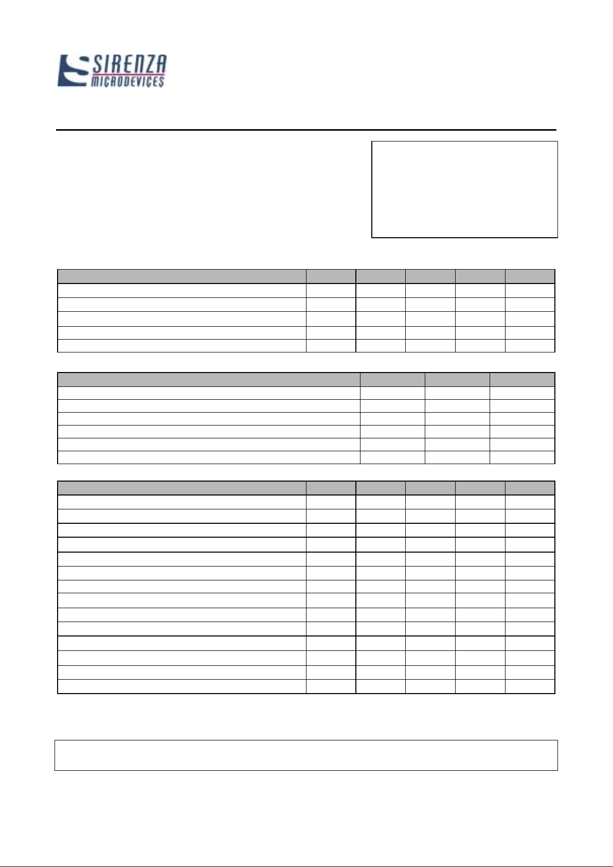
Standard Operating Conditions
Parameter Symbol Min Nom Max Units
Frequency Range
F
869 894 MHz
Supply (Drain) Voltage
VD
28 VDC
Input and Output Impedance
Ω
50 Ohms
Load Impedance for Stable Operation (All Phases) VSWR 10/1
Baseplate Temperature T
OP
-20 +90 ºC
Maximum Ratings
Parameter
Symbol Value Units
Supply (Drain) Voltage VDD 35 VDC
Input RF Power PIN +20 dBm
Load Impedance for continuous operation without damage VSWR 5/1
Base Plate Temperature: Operating with no RF present 90 ºC
Lead Temperature during reflow soldering +210 ºC
Storage Temperature T
STG
-40 to +100 ºC
Performance at 25ºC
Parameter Symbol Min Nom Max Units
Supply Voltage
V
D1,2
27.8 28.0 28.2 VDC
Power Output at 1 dB Compression (single tone)
P-1
7 8 W
Gain at 1W Output (CW)
G
30.0 32.0 34.0 dB
Gain Flatness over frequency at 1W Output (CW)
∆G
0.2 0.4 dB
Input Return Loss at 1W Output (CW) (50 Ω Ref)
iRL
14 20 dB
Quiescent Current (total)
IDQ
930 mA
Drain Efficiency at 8W CW output
ηD
22 25 %
Drain Efficiency at 1W CDMA output (Single Carrier IS-95B)
ηD
3.5 %
ACPR at 1W CDMA Power Output (Single Carrier IS-95B)
-51 dBc
ALT-1 PR at 1W CDMA Output (Single Carrier IS-95B)
-80 dBc
3rd order IMD at 8W PEP (two- tone; 1MHz ∆F)
-30 -28 dBc
3rd order IMD at 1W PEP (two- tone; 1MHz ∆F)
-50 -40 dBc
Electrical Delay
3.9 ns
Deviation from linear phase (peak to peak)
0.5 deg.
Sirenza QuikPAC Data www.sirenza.com Rev. 4 (10-01-02) Page 2 of 2
XD010-42S
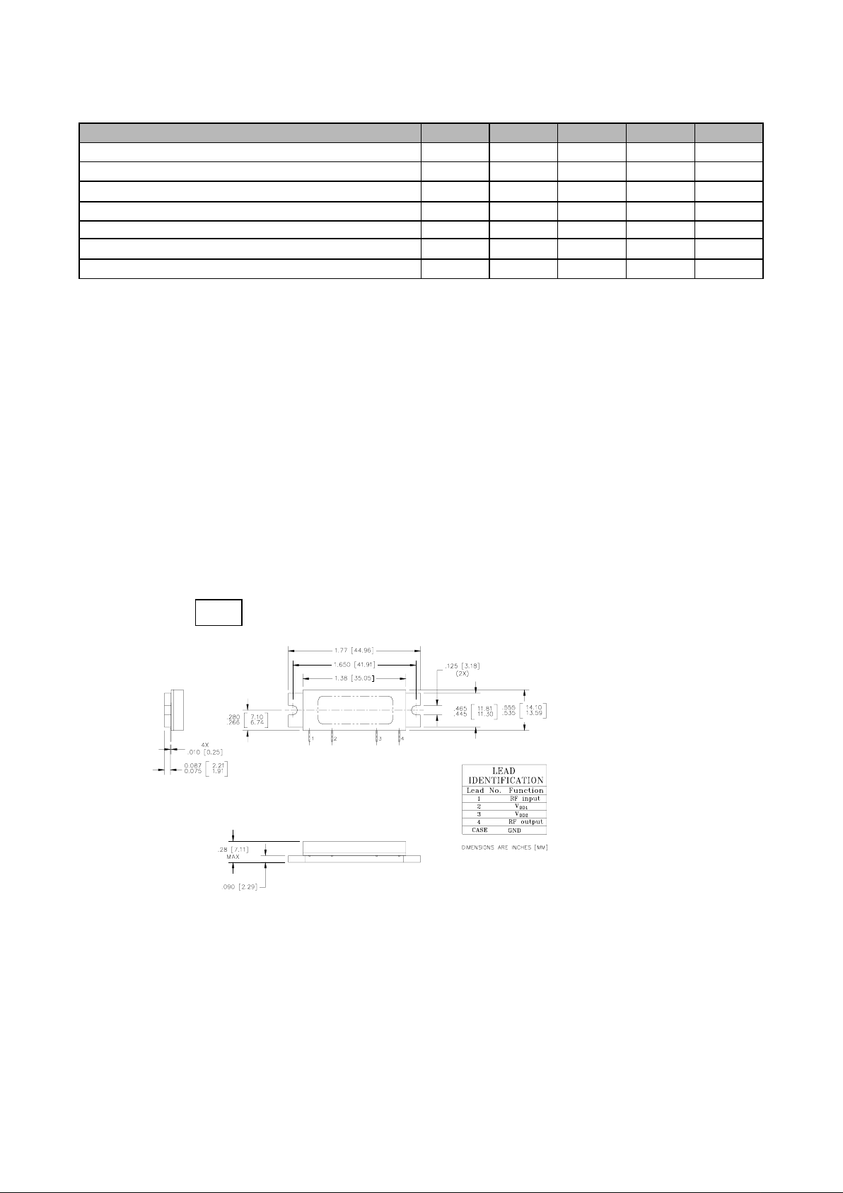
Performance Over Temperature
Parameter Symbol Min Nom Max Units
Power Output at 1 dB Compression (single tone)
P-1
8 W
Gain at 1W Output (CW)
G
32.0 dB
Gain Flatness over frequency at 1W Output (CW)
∆G
0.2 0.4 dB
Input Return Loss at 1W Output (CW) (50 Ω Ref)
iRL
18.0 dB
Drain Efficiency at 8W CW Output
ηD
25 %
Drain Efficiency at 1W CDMA Output (Single Carrier IS-95B)
ηD
3.5 %
ACPR at 1W CDMA Output (Single Carrier IS-95B)
-49 dBc
Notes:
The "Preliminary" designation on this data sheet indicates this product has not yet entered production. The data supplied
here is derived from engineering development and pilot production testing and may change.
The internal generated gate voltage is thermally compensated to maintain constant quiescent current over the temperature
range listed in the data sheet. No compensation is provided for gain changes with temperature. This can only be provided
with AGC external to the module
Internal RF decoupling is included on all bias leads. No additional bypass elements are required, however some
applications may require energy storage on the drain leads to accommodate time-varying waveforms.
The RF leads are internally connected to DC ground. Do not apply DC voltages to the RF leads. Care must be taken to
protect against video transients that may damage the active devices.
Package
This model is available in the D4F (H12109) package style.
Please see the applicable outline drawing for detailed dimensions.
D4F
 Loading...