

XEMOD QPP-033 Datasheet
XEMOD RESERVES THE RIGHT TO MAKE CHANGES TO THIS SPECIFICATION WITHOUT FURTHER NOTICE. BEFORE THE
PRODUCT DESCRIBED HERE IS WRITTEN INTO SPECIFICATIONS OR USED IN CRITICAL APPLICATIONS, THE PERFORMANCE
CHARACTERISTICS SHOULD BE VERIFIED BY CONTACTING XEMOD.
Xemod QuikPAC Data www.xemod.com Rev. A (10-17-01) Page 1 of 1
QPP-033
QPP-033
Preliminary 200W, 832-870MHz
QuikPAC Module Data Class AB Power Stage
General description:
The QPP-033 QuikPAC™ RF power module is an impedancematched Class AB amplifier stage designed for use in the output
stage of linear RF power amplifiers for CDMA base stations. The
power transistors are fabricated using Xemod’s advanced design
LDMOS process. The gate terminal is connected directly to the
control voltage pin, allowing direct control of the bias. The user must
supply the proper value of V
GS
to set the desired quiescent current.
Features:
Single Polarity Operation
Matched for 50 Ω RF interfaces
XeMOS FET Technology
Stable Performance
QuikPAC System Compatible
QuikClip or Flange Mounting
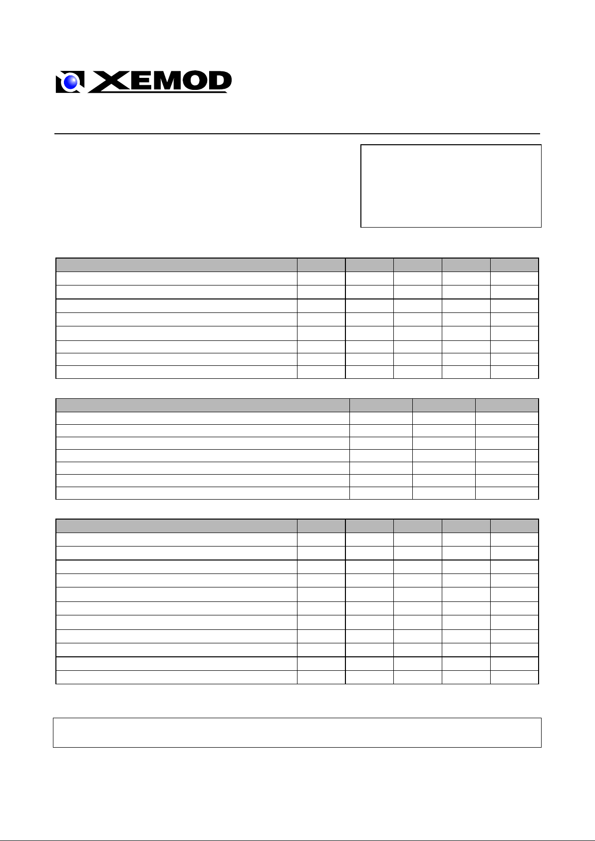
Standard Operating Conditions
Parameter Symbol Min Nom Max Units
Frequency Range
F
832 870 MHz
Supply (Drain) Voltage
VD
26.0 28.0 32.0 VDC
Bias (Gate) Voltage
VG
3.0 3.5 5.0 VDC
Bias (Gate) Current, Average
IG
2.0 mA
RF Source & Load Impedance
Ω
50 Ohms
Load Impedance for Stable Operation (All Phases) VSWR 10:1
Operating Baseplate Temperature T
OP
-20 +90 ºC
Output Device Thermal Resistance, Channel to Baseplate
Θjc
0.4 ºC/W
Maximum Ratings
Parameter
Symbol Value Units
Supply (Drain) Voltage VD 35 VDC
Control (Gate) Voltage, VD = 0 VDC VG 15 VDC
Input RF Power PIN 20 W
Load Impedance for continuous operation without damage VSWR 3:1
Output Device Channel Temperature 200 ºC
Lead Temperature during reflow soldering +210 ºC
Storage Temperature T
STG
-65 to +150 ºC
Performance at 28VDC & 25ºC
Parameter Symbol Min Nom Max Units
Supply (Drain) Voltage
V
D1,2
27.8 28.0 28.2 VDC
Quiescent Current (total)
IDQ
1,800 2,000 2,200 mA
Peak Envelope Power at 1 dB Compression (two tone)
P-1
200 220 W
Gain at 40W PEP (two tone)
G
13.0 13.5 dB
Gain Variation over frequency at 40W Output (two tone)
∆G
0.2 0.5 dB
Input Return Loss (50 Ω Ref) at 40W PEP (two tone)
IRL
11.0 15.0 dB
Drain Efficiency at 200W PEP (two tone)
η
32 36 %
3rd Order IMD Product (2 tone at 200W PEP;1 MHz spacing)
-30 -28 dBc
IMD Variation – 100 kHz to 25 MHz tone spacing
1.0 2.0 dB
2nd Harmonic at 200W P
out
(single tone)
dBc
3rd Harmonic at 200W P
out
(single tone)
dBc

Xemod QuikPAC Data www.xemod.com Rev. A (10-17-01) Page 2 of 2
QPP-033
Performance at 28VDC & 25ºC (continued)
Parameter Symbol Min Nom Max Units
Group (Signal) Delay
τd
4.7 4.9 ns
Transmission Phase Flatness
0.5 1.0 degrees
CDMA(1) ACPR at 40W Pout AVG
-46 -48 dB
CDMA(1) ACPR at 20W Pout AVG
-52 -53 dB
CDMA(1) Drain Efficiency at 40W Pout AVG
η
20 21 %
CDMA(1) Drain Efficiency at 20W Pout AVG
η
13 15 %
(1) CDMA test signal is single carrier IS-95
Notes:
The "Preliminary" designation on this data sheet indicates this product has not yet entered the volume production stage.
The data supplied here is derived from engineering development and pilot production testing and may change.
This QuikPAC module requires an externally supplied gate voltage (VGS) on each gate lead (pins 1 and 5) to set the
operating point (quiescent current (I
DQ
)) of the power transistors. VGS may be safely set to any voltage in the range listed in
the table. This permits a wide range of quiescent current to be used. Since the operating characteristics of the module will
vary as I
DQ
changes, the proper bias setting will depend on the application. The data provided in the Performance section of
this data sheet was obtained with I
DQ
set to a value within the range listed (a nominal value ±10%). This particular value was
chosen to provide a gain, IMD performance, and efficiency that are suitable for many applications but may not be optimum
for a specific design requirement.
Gate voltage must be applied coincident with or after application of the drain voltage to prevent potentially destructive
oscillations. Bias voltages should never be applied to a module unless it is terminated on both input and output.
The V
GS
corresponding to a specific IDQ will vary from module to module and may vary between the two sides of a dual RF
module by as much as ±0.10 volts. This is due to the normal die-to-die variation in threshold voltage of LDMOS transistors.
Since the threshold voltage of an LDMOS transistor changes with temperature, it is usually necessary to use a V
GS
supply
that is compensated to maintain constant I
DQ
over temperature if operation over a wide temperature range is desired.
Internal RF decoupling is included on all bias leads. No additional bypass elements are required, however some
applications may require energy storage on the drain leads to accommodate time-varying waveforms.
The RF leads are internally protected against DC voltages up to 100V. Care should be taken to avoid video transients that
may damage the active devices.
 Loading...