

Xemics XE88LC04ME028, XE88LC03ME028, XE88LC02ME028, XE88LC05ME028, XE88LC01ME028 Datasheet
Cool Solutions
XEMICS SA, Switzerland. Tel: +41 32 720 51 70 Fax: +41 32 720 57 70 e-mail: info@xemics.com web: www.xemics.com
XX-XE88LC05
Data Sheet
XE88LC05
Ultra Low-Power Microcontroller with
ADC and DACs for Sensor Conditioning
General Description
The XE88L C05 is an ultra l ow-power microcon troller unit
(MCU) associated with a versatile analo
g
-to-digital con-
verter (ADC) includin
g
a programmable offset and gain
pre-amplifier (PGA) and di
g
ital-to-analog converters
(DACs).
XE88LC05 is available with on chip Multiple-Time-Pro-
g
rammable (MTP) Flash program memory.
Applications
• Internet connected appliances
• Portable, battery operated instruments
• Piezoresistive brid
g
e sensors
• 4-20 mA bus sensors
• 0.5 - 4.5 V sensors
• HVAC control
• Motor control
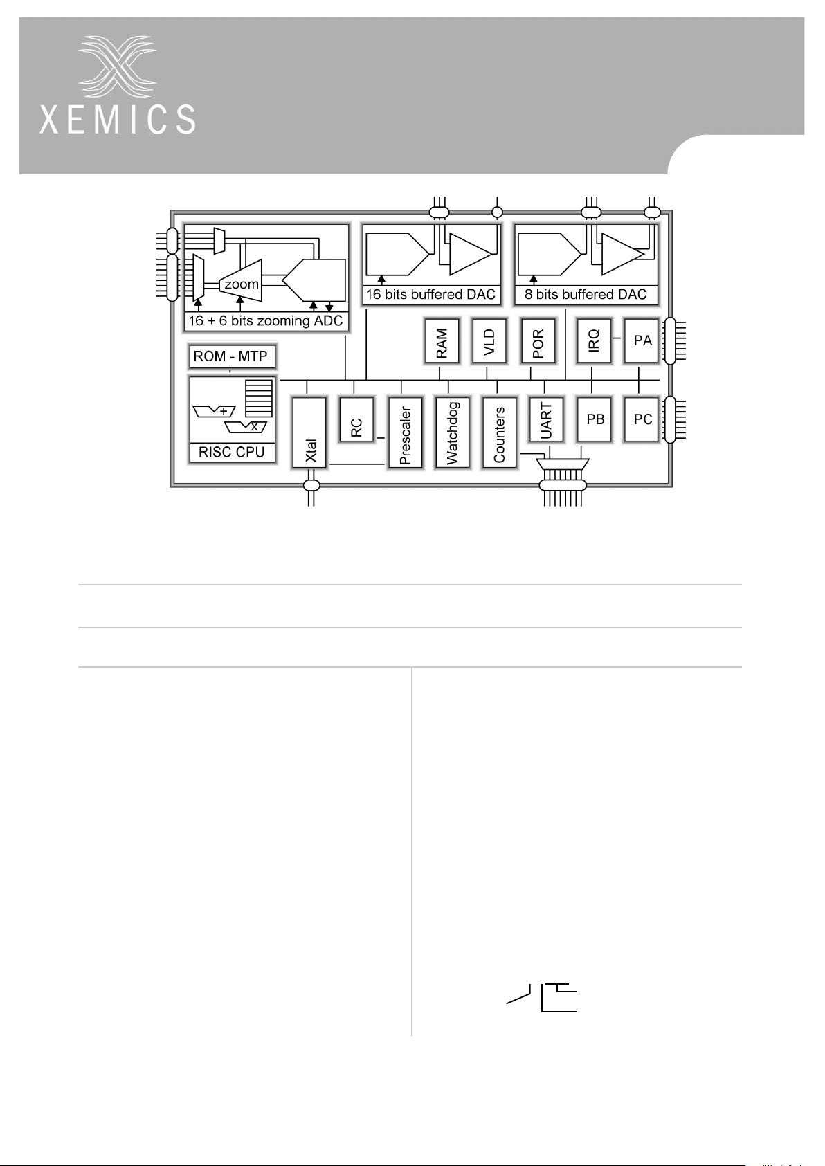
Key product Features
• Ultra low-power MCU (300 µA at 1 MIPS)
• Low-volta
g
e operation (2.4 - 5.5 V supply voltage)
• 22 kB (8 kW) MTP, 512 B RAM
•Voltage or current output DACs
• Buffered si
g
nal-DAC (up to 16 bits)
• Buffered bias-DAC (up to 10 mA drive)
• Low-power, high resolution ZoomingADC
• up to 10 bits zoom
• up to 16 bits ADC
• 4 x 2 or 7 x 1 PGA-ADC input multiplexer
•Analo
g
matrix switchin
g
• RC and crystal oscillators
• 5 reset, 16 interrupt, 8 event sources
Ordering Informatio n
Nomenclature: (XX marks pre-production samples)
;(/&0(
program memory
M: MTP
temperature
I: -40 to 85 °C
TQFP64 package
Low-Power Microcontroller
XX-XE88LC01
XX/D010-060 Produ ct Prel im inary Specification Page 2
Detailed Pin Description
Pin
Description
Position
Function
name
Second function
name
Type
1 PA(0) testin Input
Input of Port A/
Data input for test and MTP programming/
Counter A input
2 PA(1) testck Input
Input of Port A/
Data clock for test and MTP programming/
Counter B input
3 PA(2) Input
Input of Port A/
Counter C input/ Counter capture input
4 PA(3) Input
Input of Port A/
Counter D input/ Counter capture input
5 PA(4) Input Input of Port A
6 PA(5) Input Input of Port A
7 PA(6) Input Input of Port A
8 PA(7) Input Input of Port A
9 PC(0) Input/Output Input-Output of Port C
10 PC(1) Input/Output Input-Output of Port C
11 PC(2) Input/Output Input-Output of Port C
12 PC(3) Input/Output Input-Output of Port C
13 PC(4) Input/Output Input-Output of Port C
14 PC(5) Input/Output Input-Output of Port C
15 PC(6) Input/Output Input-Output of Port C
16 PC(7) Input/Output Input-Output of Port C
17 PB(0) testout Input/Output/Analog
Input-Output-Analog of Port B/
Data output for test and MTP programming/
PWM output
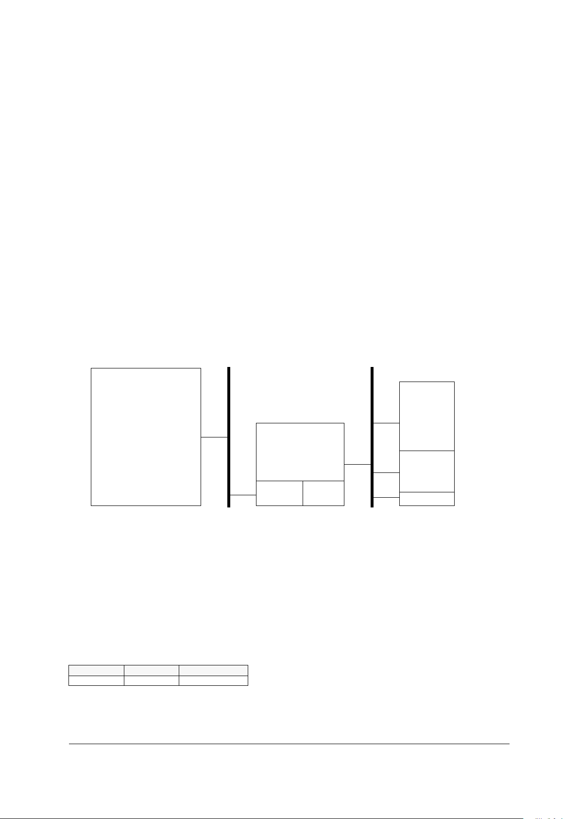
Table 1.2: Pin-out of the XE88LC05 in TQFP64
Pinout of the XE88LC05 in TQFP64 package
PA(0)
PA(1)
PA(2)
PA(3)
PA(4)
PA(5)
PA(6)
PA(7)
PC(0)
PC(1)
PC(2)
PC(3)
PC(4)
PC(5)
PC(6)
PC(7)
1
2
3
4
5
6
7
8
9
10
11
12
13
14
15
16
18 20 22 24 26 28 30
48
47
46
45
44
43
42
41
40
39
38
37
36
35
34
33
63 61 59 57 55 53 51
PB(0)
PB(1)
PB(2)
PB(3)
PB(4)
PB(5)
PB(6)
PB(7)
DAB_Out
DAB_AO_p
DAB_AO_m
DAB_AI_p
DAB_AI_m
AC_R(0)
AC_R(1)
AC_A(0)
AC_A(1)
AC_A(2)
AC_A(3)
AC_A(4)
AC_A(5)
AC_A(6)
AC_A(7)
AC_R(2)
AC_R(3)
OscIn
OscOut
RESET
Vmult
TEST
Vreg
Vss_Vreg
Vss
Vbat
DAS_Out
DAS_AI_p
DAS_AI_m
DAS_AO
XEMICS
DAB_R_p
DAB_R_m
XE88LC05MI
N9K1444
9920
device type
production
packaging date
lot identification
Low-Power Microcontroller
XX-XE88LC01
XX/D010-060 Produ ct Prel im inary Specification Page 3
18 PB(1) Input/Output/Analog
Input-Output-Analog of Port B/
PWM output
19 PB(2) Input/Output/Analog Input-Output-Analog of Port B
20 PB(3) SOU Input/Output/Analog
Input-Output-Analog of Port B,
Output pin of USRT
21 PB(4) SCL Input/Output/Analog
Input-Output-Analog of Port B/
Clock pin of USRT
22 PB(5) SIN Input/Output/Analog
Input-Output-Analog of Port B/
Data input or input-output pin of USRT
23 PB(6) Tx Input/Output/Analog
Input-Output-Analog of Port B/
Emission pin of UART
24 PB(7) Rx Input/Output/Analog
Input-Output-Analog of Port B/
Reception pin of UART
25 DAB_R_p Analog Positive reference of bias DAC
26 DAB_R_m Analog Negative reference of bias DAC
27 DAB_Out Analog Output of bias DAC
28 DAB_AO_p Analog Highest potential output of bias DAC buffer
29 DAB_AO_m Analog Lowest potential output of bias DAC buffer
30 DAB_AI_p Analog Positive input of bias DAC buffer
31 DAB_AI_m Analog Negative input of bias DAC buffer
32 Not connected Spare pins to be connected to negative power supply
33 TEST/Vhigh Vhigh Special Test mode/High voltage for MTP programming
34 Not connected Spare pins to be connected to negative power supply
35 AC_R(3) Analog Highest potential node for 2nd reference of ADC
36 AC_R(2) Analog Lowest potential node for 2nd reference of ADC
37 AC_A(7) Analog ADC input node
38 AC_A(6) Analog ADC input node
39 AC_A(5) Analog ADC input node
40 AC_A(4) Analog ADC input node
41 AC_A(3) Analog ADC input node
42 AC_A(2) Analog ADC input node
43 AC_A(1) Analog ADC input node
44 AC_A(0) Analog ADC input node
45 AC_R(1) Analog Highest potential node for 1st reference of ADC
46 AC_R(0) Analog Lowest potential node for 1st reference of ADC
47-50 Not connected Spare pins to be connected to negative power supply
51 DAS_Out Analog Output of signal DAC
52 DAS_AI_p Analog Positive input of signal DAC buffer
53 DAS_AI_m Analog Negative input of signal DAC buffer
54 DAS_AO Analog Output of signal DAC buffer
55 Vbat Power Positive power supply
56 Vss Power Negative power supply, connected to substrate
57 Vss_Reg Power Digital negative power supply, must be equal to Vss
58 Vreg Analog Regulated supply
59 Not connected Spare pins to be connected to negative power supply
60 Vmult Analog Pad for optional voltage multiplier capacitor
61 RESET Input Reset pin (active high)
62 OscOut ptck Analog/Input
Connection to Xtal/
Peripheral clock for test and MTP program min g
63 OscIn ck_cr Analog/Input
Connection to Xtal/
CoolRISC clock for test and MTP programming
64 - - Do not connect, or VSS
Pin
Description
Position
Function
name
Second function
name
Type
Table 1.2: Pin-out of the XE88LC05 in TQFP64
Low-Power Microcontroller
XX-XE88LC01
XX/D010-060 Produ ct Prel im inary Specification Page 4
XE88LC05xI Electrical Characteristics
Note:
1) Power supply: 2.4 V - 5.5 V, at 27°C; min voltage of XX version may be higher, max frequency
of current XX version is 2 MHz
Note:
2) Temperature < 85°C
Note:
3) Output not loaded.
Note:
4) Current requirement can be divided by a factor of 2 or 4 by reducin
g
the speed accordingly.
Note:
5) More cycles possibl e durin
g
development, with restraint retention
Operation conditions min typ max Unit Remarks
Power supply
ROM version 2.4 5.5 V
MTP version 2.4 5.5 V
Current re quirement
CPU running
at 1 MIPS
310 uA 1
CPU running
at 32 kHz
on Xtal,
RC off
10 uA 1
CPU halt,
timer on Xtal,
RC off
1uA 1
CPU halt,
timer on Xtal,
RC ready
1.7 uA 1
CPU halt,
Xtal off
timer on RC
at 100 kHz
1.4 uA 1
CPU halt,
ADC 12 bits
at 4 kHz
200 uA 1,4
CPU halt,
ADC 12 bits
at 4 kHz,
PGA gain 100
250 uA 1,4
CPU at 1 MIPS,
ADC 12 bits and DAC
10 bits
at 4 kHz
660 uA 1,3,4
CPU at 1 MIPS,
ADC 12 bits and DAC
10 bits
at 4 kHz,
PGA gain 10
685 uA 1,3,4
CPU at 1 MIPS,
ADC 12 bits and DAC
10 bits
at 4 kHz,
PGA gain 100
710 uA 1,3,4
CPU at 1 MIPS,
ADC 12 bits and DAC
10 bits
at 4 kHz,
PGA gain 1000
785 uA 1,3,4
Voltage level
detection
15 uA
MTP
Prog. voltage 10.3 10.8 V
Erase time 3 30 s
Write/Erase cycles 10 100 5
Data retention 10 year 2
Current requirement of the XE88LC05
Low-Power Microcontroller
XX-XE88LC01
XX/D010-060 Produ ct Prel im inary Specification Page 5
CPU
The XE88LC05 CPU is a low power RISC core. It has 16 internal registers for efficient implementa tion of th e C compiler. Its instruction set is made of 35
g
eneric instructions, all coded on 22 bit s, with 8 add ressing modes. All instruc-
tions are executed in one clock cycle, includin
g
conditional jumps and 8x8 multiplication.
A complete tool suite for development is available from XEMICS, includin
g
programmer, C-compiler, assembler,
simulator, linker, all inte
g
rated in a modern and efficient graphical user interface.
Memory organisation
The CPU uses a Harvard architecture, so that memory is organised in two separated fields: program memory and
data memory. As both memory are separated, the central processin
g
unit can read/write data at the same time it
loads an instruction. Peripherals and system control re
g
isters are mapped on da ta memory space.
Pro
g
ram memory is made in one page (program page full size is 65’536 instructions). Data is made of several 256
bytes pa
g
es.
Program memory
The program memory is implemented as Multiple Time Programmable (MTP) Flash memory.
The power consumption of MTP is linear with the access frequency (no si
g
nificant st atic current).
Memory sizes:
• Flash MTP: 8192 x 22 bits (= 22 kBytes)
block size address
MTP 8192 x 22 H0000 - H1FFF
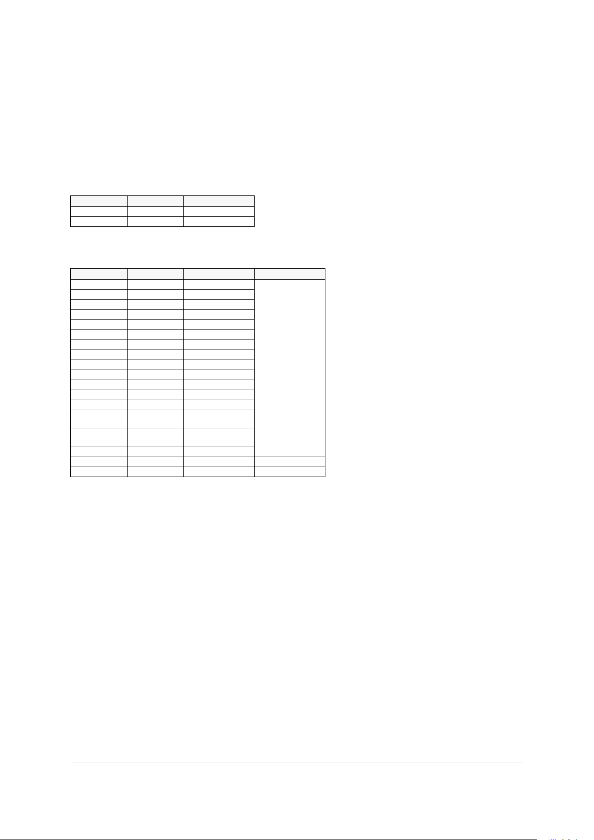
Program addresses
Memory organization
CPU
Program
memory
Registers
Peripherals
RAM
Program address bus
Data address bus
22 bits wide 8 bits wide
CPU
registers
Instruction
pipeline
8k instructions
512 Bytes
Low-Power Microcontroller
XX-XE88LC01
XX/D010-060 Produ ct Prel im inary Specification Page 6
Data memor y
The data memory is implemented as static Random-Access Memory (RAM). The size is 512 x 8 bits plus 8 low power re
g
isters that require very low current when addres sed, programs using these registers instead of RAM will spare
even more current.
Note:
The re
g
isters in Data memory are not related to the CPU registers.
Peripherals mapping
Peripherals
The XE88L C05 incl udes usu al micro controll er peri pherals and some other b locks mor e specif ic to lo w-voltage or
mixed-si
g
nal operation. They are 3 paralle l ports, one input port (A), one IO and anal og port (B) with analog switch-
in
g
capabilities and one general purpose IO port (C). A watchdog is available, connected to a prescaler. Four 8-bit
counters, with ca pture, PWM and chai nin
g
capabilities ar e availab le. The UA RT can ha ndle t ransmissio n speeds as
hi
g
h as 38kbaud.
Low-power low-voltage blocks include a voltage level detector, t wo osci llator s (o ne inte rnal 0.1 -4 MHz RC osc illat or
and a 32 kHz crystal oscillator) and a specific re
g
ulation scheme that largely uncouples current requirement from
external power supply (usual CMOS ASICs require much more c urre nt at 5 .5 V than they need at 2.4 V. This is not
the case for the XE88LC05).
Analo
g
blocks: acquisitio n path, bias DAC and signal DAC are defined below. All these blocks operate on 2.4 - 5.5
V power supply ran
g
e.
block size address
LP RAM 8 x 8 H0000 - H0007
RAM 512 x 8 H0080 - H027F
RAM addresses
block size address Page
LP RAM 8x8 H0000 -H0 007
Page 0
System control 16x8 H0010-H001F
Port A 8x8 H0020-H 0 027
Port B 8x8 H0028-H002F
Port C 4x8 H0030-H0033
Port D 4x8 H0034-H0037
MTP 4x8 H0038-H003B
Event 4x8 H003C-H003F
Interrupts control 8x8 H0040-H0047
reserved 8x8 H0048-H004F
UART 8x8 H0050-H0057
Counters 8x8 H0058-H005F
Zooming ADC 8x8 H0060-H0067
Reserved 12x8 H0068-H0073
DACs 8x8 H0074-H007B
Other
(VLD)
4x8 H007C-H007F
RAM1 128x8 H0080 - H00FF
RAM2 256x8 H0100 - H01FF Page 1
RAM3 128x8 H0200 - H027F Page 2
Peripherals addresses
 Loading...