

Xemics XE88LC05ME015, XE88LC04ME026, XE88LC04ME015, XE88LC03ME026, XE88LC03ME015 Datasheet
...
Cool Solutions
XEMICS SA, Switzerland. Tel: +41 32 720 51 70 Fax: +41 32 720 57 70 e-mail: info@xemics.com web: www.xemics.com
XX/XE88LC03
Data Sheet
XE88LC03
Ultra Low-Power Low-Voltage
Microcontroller
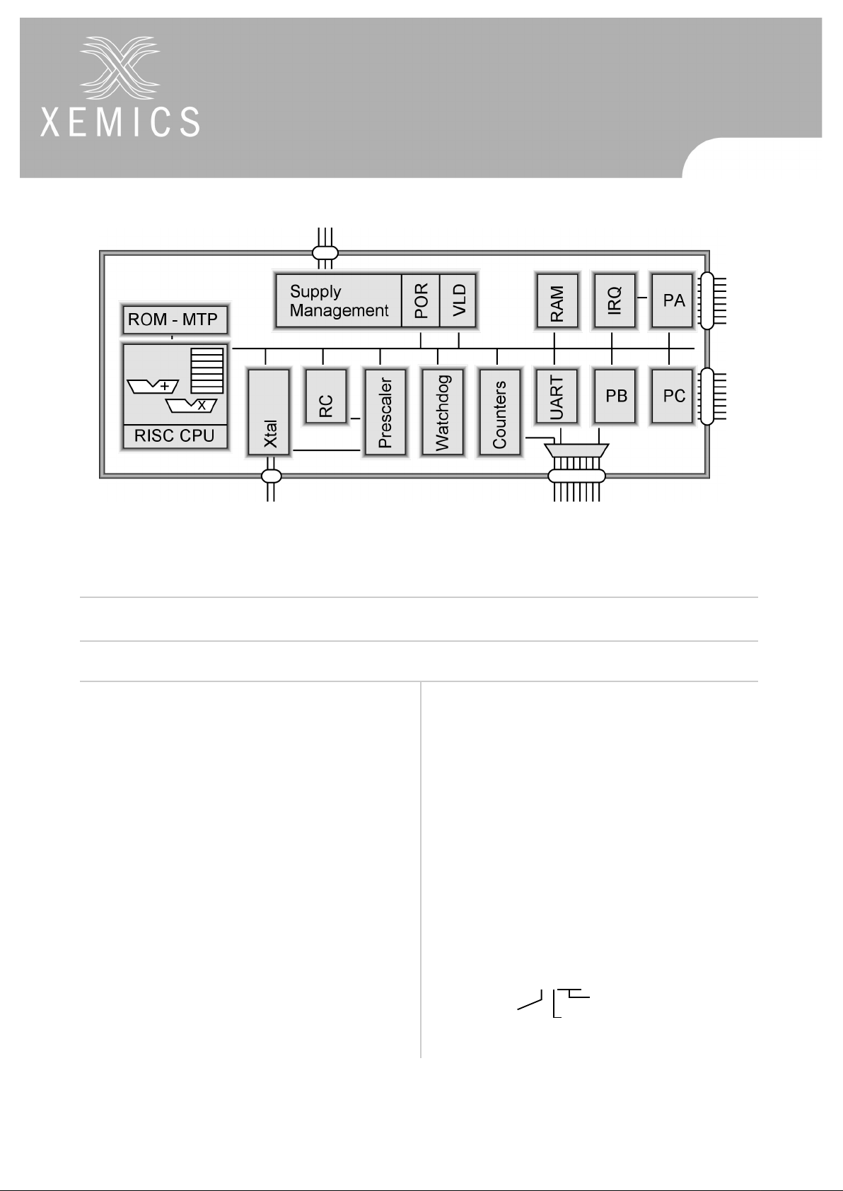
General Description
The XE88LC03 is an ultra low-power low-voltage microcontroller unit (MC U) w it h ext r emely h i
g
h efficiency, allow-
in
g
for 1 MIPS at 300uA at 2.4 V, and 8 x 8 bits mult iplyi n
g
in one clock cycle.
XE88LC03 is available with on chip Multiple-Time-Pro-
g
rammable (MTP) program memory.
Applications
• Internet connected appliances
• Portable, battery operated instruments
• RF system supervisor
• Remote control
• HVAC control
Key product Features
• Ultra low-power MCU
• 300 uA at 1 MIPS operation
• 6 uA at 32 kHz operation
• 1 uA time keepin
g
• Low-voltage operation (2.4 - 5.5 V supply voltage)
• 22 kB (8 kW) MTP, 512 B RAM
• 4 counters
•PWM
• UART
•Analo
g
matrix switchin
g
• independant RC and crystal oscillators
• 5 reset, 15 interrupt, 8 event sources
Ordering Informatio n
Nomenclature: (XX identifies pre-production products)
XE88LC03ME012
program memory
M: MTP
temperature
I: -40 to 85 °C
packa
g
e: 015: SO28
026: TQFP32
Low-Power Microcontroller
XX-XE88LC01
XX/D010-060 Produ ct Prel im inary Specification Page 2
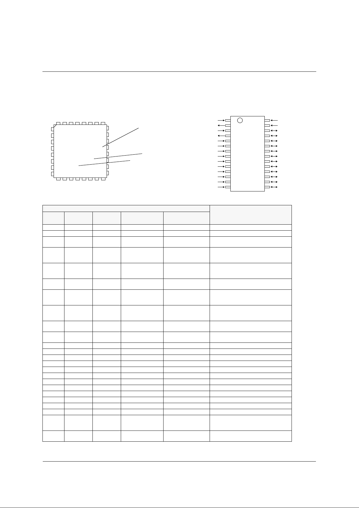
Detailed Pin Description
Pin
Description
Position
in SO28
Position in
TQFP32
Function
name
Second function
name
Type
1 13 Vbat Power Positive power supply
2 14 Vreg Analog Regulated supply
3 15 TEST/Vhigh Vhigh Special
Test mode/High voltage for MT P
programing
4 16 OscOut ptck Analog/Input
Connection to Xtal/
Peripheral clock for test and MTP
programing
5 17 OscIn ck_cr Analog/Input
Connection to Xtal/
CoolRISC clock for test and MTP
programing
6 18 Vss Power
Negative power supply, connected to
substrate
7 19 PA(0) testin Input
Input of Port A/
Data input for test and MTP programing/
Counter A input
8 20 PA(1) testck Input
Input of Port A/
Data clock for test and MTP programing/
Counter B input
9 21 PA(2) Input
Input of Port A/
Counter C input/ Counter capture input
10 22 PA(3) Input
Input of Port A/
Counter D input/ Counter capture input
11 23 PA(4) Input Input of Port A
12 24 PA(5) Input Input of Port A
13 25 PA(6) Input Input of Port A
14 26 PA(7) Input Input of Port A
15 27 PC(0) Input/Output Input-Output of Port C
16 28 PC(1) Input/Output Input-Output of Port C
17 29 PC(2) Input/Output Input-Output of Port C
18 30 PC(3) Input/Output Input-Output of Port C
31 PC(4) Input/Output Input-Output of Port C
32 PC(5) Input/Output Input-Output of Port C
1 PC(6) Input/Output Input-Output of Port C
2 PC(7) Input/Output Input-Output of Port C
19 3 PB(0) testout Input/Output/Analog
Input-Output-Analog of Port B/
Data output for test and MTP programing/
PWM output
20 4 PB(1) Input/Output/Analog
Input-Output-Analog of Port B/
PWM output
Pin-out of the XX-XE88LC03 in SO28 and TQFP32
1
2
3
4
5
6
7
8
9
10
11
12
13
14
28
27
26
25
24
23
22
21
20
19
18
17
16
15
XEMICS
XX88LC03xI015
9920
VBat
VReg
TEST/VHigh
OSCout
OSCin/FREQin
Vgnd
PA[0]
PA[1]
PA[2]
PA[3]
PA[4]
PA[5]
PA[6]
PA[7]
RCRes
RESET
PB[7]
PB[6]
PB[5]
PB[4]
PB[3]
PB[2]
PB[1]
PB[0]
PC[3]
PC[2]
PC[1]
PC[0]
Pinout of the XX-XE88LC03 in SOP28 packagePinout of the XX-XE88LC03 in TQFP32 package
1
2
3
4
5
6
7
810 12 14 16
18
20
22
24262830
XEMICS
XX88LC03MI
N9K1444
9920
device type
production
packaging date
lot identification
Low-Power Microcontroller
XX-XE88LC01
XX/D010-060 Produ ct Prel im inary Specification Page 3
XE88LC03xI Electrical Characteristics
Note:
1)Power supply: 2.4 V - 5.5 V, at 27°C; min voltage of XX version may be higher.
CPU
The XE88LC03 CPU is a low power RISC core. It has 16 internal registers for efficient implementa tion of th e C compiler. Its instruction set is made of 35
g
eneric instructions, all coded on 22 bit s, with 8 add ressing modes. All instruc-
21 5 PB(2) Input/Output/Analog Input-Output-Analog of Port B
22 6 PB(3) SOU Input/Output/Analog
Input-Output-Analog of Port B,
Output pin of USRT
23 7 PB(4) SCL Input/Output/Analog
Input-Output-Analog of Port B/
Clock pin of USRT
24 8 PB(5) SIN Input/Output/Analog
Input-Output-Analog of Port B/
Data input or input-output pin of USRT
25 9 PB(6) Tx Input/Output/Analog
Input-Output-Analog of Port B/
Emission pin of UART
26 10 PB(7) Rx Input/Output/Analog
Input-Output-Analog of Port B/
Reception pin of UART
27 11 RESET Input Reset pin (active high)
28 12 RCRes Analog Optional external resistor for RC oscillator
Operation conditions min typ max Unit Remarks
Power supply
2.4 5.5 V 1
Current re quirement
CPU running
at 1 MIPS
310 uA 1
CPU running
at 32 kHz
on Xtal,
RC off
10 uA 1
CPU halt,
timer on Xtal,
RC off
1uA 1
CPU halt,
timer on Xtal,
RC ready
1.7 uA 1
CPU halt,
Xtal off
timer on RC
at 100 kHz
1.4 uA 1
Voltage level
detection
15 uA 1
MTP
Prog. voltage 10.3 10.8 V
Erase time 3 30 s
Write/Erase cycles 10 100
Data retention 10 year
Current requirement of the XE88LC03
Pin
Description
Position
in SO28
Position in
TQFP32
Function
name
Second function
name
Type
Pin-out of the XX-XE88LC03 in SO28 and TQFP32
Low-Power Microcontroller
XX-XE88LC01
XX/D010-060 Produ ct Prel im inary Specification Page 4
tions are executed in one clock cycle, including conditional jumps and 8x8 multiplication, therefore the XE88LC03
runs at 1 MIPS on a 1 MHz clock.
A complete tool suite for development is available from XEMICS, includin
g
programmer, C-compiler, assembler,
simulator, linker, all inte
g
rated in a modern and efficient graphical user interface.
NAME Par amet ers res op1 op2 FUNCTION MODIF.
JUMP
addr:16 PC0 <- addr
- , - , - , -
ip PC0 <- ip
Jcc
addr:16 if cc then PC0 <- addr
ip if cc then PC0 <- ip
CALL
addr:16 PCn <- PCn-1 (n>1), PC1 <- PC0+1, PC0 <- addr
ip PCn <- PCn-1 (n>1), PC1 <- PC0+1, PC0 <- ip
CALLS
addr:16 ip <- PC0+1, PC0 <- addr:16
ip ip <- PC0+1, PC0 <- ip
RET PCn-1 (n>0) <- PCn
- , - , - , -
RETS PC0 <- ip
RETI PCn-1 (n>0) <- PCn, GIE <- 1
PUSH PCn <- PCn-1 (n>1), PC1 <- ip, PC0 <- PC0+1
POP ip <- PC1, PCn-1 (n>1) <- PCn, PC0 <- PC0+1
MOVE
reg, data:8 reg data
res <- op1
- , - , Z , areg1, reg2 reg1 reg2
reg, eaddr reg eaddr
eaddr, reg eaddr reg
- , - , - , -
addr:8, dat a:8 addr data
CMVD reg1, reg2 reg1 reg2 if C=0 then res <- op1
- , - , Z , a
CMVS reg, eaddr reg eaddr if C=1 then res <- op1
SHL
reg1, reg2 reg1 reg2
res(bitn) <- op1(bitn-1) (0<n<8), res(0) <- 0, C <- op1(7) C, V, Z, areg reg reg
reg, eaddr reg eaddr
SHLC
reg1, reg2 reg1 reg2
res(bitn) <- op1(bitn-1) (0<n<8), res(0) <- C, C <- op1(7) C, V, Z, areg reg reg
reg, eaddr reg eaddr
SHR
reg1, reg2 reg1 reg2
res(bitn-1) <- op1(bitn) (0<n<8), res(7) <- 0, C <- op1(0) C, V, Z, areg reg reg
reg, eaddr reg eaddr
SHRC
reg1, reg2 reg1 reg2
res(bitn-1) <- op1(bitn) (0<n<8), res(7) <- C, C <- op1(0) C, V, Z, areg reg reg
reg, eaddr reg eaddr
SHRA
reg1, reg2 reg1 reg2
res(bitn-1) <- op1(bitn) (0<n<8), res(7) <- op1(7), C <- op1(0) C, V, Z, areg reg reg
reg, eaddr reg eaddr
CPL1
reg1, reg2 reg1 reg2
res <- NOT (op1) -, -, Z, areg reg reg
reg, eaddr reg eaddr
CPL2
reg1, reg2 reg1 reg2
res <- NOT (op1) +1, if op1 = 0 then C = 1 C, V, Z, areg reg reg
reg, eaddr reg eaddr
CPL2C
reg1, reg2 reg1 reg2
res <- NOT (op1) +C, if op1 = 0 then C = 1 C, V, Z, areg reg reg
reg, eaddr reg eaddr
INC
reg1, reg2 reg1 reg2
res <- op1 +1, if overflow then C = 1 C, V, Z, areg reg reg
reg, eaddr reg eaddr
INCC
reg1, reg2 reg1 reg2
res <- op1 +C, if overflow then C = 1 C, V, Z, areg reg reg
reg, eaddr reg eaddr
Table 1.2: XE8000 Instruction Set
 Loading...