

Xembedded XVME-689-VR7 User Manual

i
XVME-689-VR7
Single-Slot VMEbus
Intel® Celeron™ M Processor Module
User Manual
2008 X
EMBEDDED
™, INC.
Printed in the United States of America

ii
Revision Description Date
A Init 02/08
B Errors in J2 and P0 pin-out 09/09
C Error Correction 02/10
Part Number 74689-VR7
Trademark Information
Brand or product names are trademarks or registered trademarks of their respective owners.
Intel and Pentium are registered trademarks and Celeron is a trademark of Intel Corporation.
Windows, Windows NT, Windows 2000 and Windows XP are registered trademarks of Microsoft
Corporation in the US and in other countries.
Copyright Information
This document is copyrighted by Xembedded, Incorporated (Xembedded) and shall not be
reproduced or copied without expressed written authorization from Xembedded.
The information contained within this document is subject to change without notice. Xembedded
does not guarantee the accuracy of the information.
WARNING
This is a Class A product. In a domestic environment this product may cause radio interference,
in which case the user may be required to take adequate measures.
Warning for European Users – Electromagnetic Compatibility
European Union Directive 89/336/EEC requires that this apparatus comply with relevant ITE
EMC standards. EMC compliance demands that this apparatus is installed within a VME
enclosure designed to contain electromagnetic radiation and which will provide protection for the
apparatus with regard to electromagnetic immunity. This enclosure must be fully shielded. An
example of such an enclosure is a Schroff 7U EMC-RFI VME System chassis, which includes a
front cover to complete the enclosure.
The connection of non-shielded equipment interface cables to this equipment will invalidate
European Free Trade Area (EFTA) EMC compliance and may result in electromagnetic
interference and/or susceptibility levels that are in violation of regulations which apply to the
legal operation of this device. It is the responsibility of the system integrator and/or user to apply
the following directions, as well as those in the user manual, which relate to installation and
configuration:
All interface cables should be shielded, both inside and outside of the VME enclosure.
Braid/foil type shields are recommended for serial, parallel, and SCSI interface cables.
Where as external mouse cables are not generally shielded, an internal mouse interface
cable must either be shielded or looped (1 turn) through a ferrite bead at the enclosure
point of exit (bulkhead connector). External cable connectors must be metal with metal
back-shells and provide 360-degree protection about the interface wires. The cable shield
must be terminated directly to the metal connector shell; shield ground drain wires alone
are not adequate. VME panel mount connectors that provide interface to external cables
(e.g.,

iii
RS232, USB, keyboard, mouse, etc.) must have metal housings and provide direct
connection to the metal VME chassis. Connector ground drain wires are not adequate.
Environmental Protection Statement
This product has been manufactured to satisfy environmental protection requirements where
possible. Many of the components used (structural parts, printed circuit boards, connectors,
batteries, etc.) are capable of being recycled.
Final disposition of this product after its service life must be accomplished in accordance with
applicable country, state, or local laws or regulations.


Table of Contents
v
Table of Contents
XVME-689-VR7........................................................................................................................... i
Table of Contents................................................................................................................................ v
Table of Figures and Tables............................................................................................................... vii
Chapter 1 – Introduction....................................................................................................... 1-1
Module Features............................................................................................................................ 1-1
Architecture...................................................................................................................................1-2
Software Support........................................................................................................................... 1-6
Operational Description................................................................................................................. 1-6
Environmental Specifications......................................................................................................... 1-7
Hardware Specifications ................................................................................................................ 1-8
VMEbus Specification................................................................................................................... 1-9
System Configuration and Expansion Options Tables..................................................................... 1-9
Chapter 2 – Installation and Setup....................................................................................... 2-1
3Jumper Settings............................................................................................................................ 2-2
Switch Settings.............................................................................................................................. 2-3
Registers........................................................................................................................................ 2-3
Front Panel Layout.........................................................................................................................2-5
Connectors..................................................................................................................................... 2-6
COM1 and COM4 (J4) Pin Definitions........................................................................................... 2-10
VMEbus P2 Connector................................................................................................................... 2-12
VMEbus P2 Connector................................................................................................................... 2-13
Installing the XVME 689-VR7 into a Backplane.......................................................................... 2-18
Enabling the PCI Ethernet Controller........................................................................................... 2-20
Chapter 3 BIOS Setup Menus............................................................................................... 3-1
3.1 Main Setup Menu.....................................................................................................................3-2
3.2 Exit Menu................................................................................................................................ 3-4
3.3 System Boot Menu...................................................................................................................3-5
3.4 POST Memory Tests................................................................................................................ 3-9
3.5 Plug and Play Configuration Menu......................................................................................... 3-12
3.6 BIOS Super I/O Configuration Menu ..................................................................................... 3-15
3.7 BIOS Super I/O Configuration Menu ..................................................................................... 3-17
3.8 Firmbase® Technology Configuration.................................................................................... 3-19
3.9 Misc. Menu............................................................................................................................ 3-20
3.10 VMEbus Master................................................................................................................... 3-24
3.12 Front Panel resources control ............................................................................................... 3-28
Chapter 4 Programming........................................................................................................ 4-1
Memory Map................................................................................................................................. 4-1
I/O Map.........................................................................................................................................4-1
IRQ Map ....................................................................................................................................... 4-3

Table of Contents
vi
PCI Device Map –............................................................................................................................4-4
VME Interface............................................................................................................................... 4-5
Software-Selectable Byte-Swapping Hardware............................................................................... 4-7
Chapter 5 XVME 990-VR7 Rear Transition Module ............................................................. 5-1
Connectors..................................................................................................................................... 5-2
Serial ATA hard drive Interface..................................................................................................... 5-3
Appendix A SDRAM and Battery Installation......................................................................... 1
Memory Type................................................................................................................................... 1
Installing SDRAM............................................................................................................................ 1
Module Battery Installation............................................................................................................... 2
Index................................................................................................................................................... 4

Table of Contents
vii
Table of Figures and Tables
Figure 1-1 XVME 689-VR7 Block Diagram ............................................................................1-6
Figure 3-1 Main Setup Menu....................................................................................................3-2
Figure 3-2 Slave Interface Submenu.......................................................................................3-26
Figure 4-1 Byte Ordering Schemes...........................................................................................4-8
Figure 4-2 Address-Invariant Translation.................................................................................4-8
Figure 4-3 Maintaining Numeric Consistency...........................................................................4-9
Figure 4-4 Maintaining Address Consistency..........................................................................4-10
Table 1-1 Maximum Video Modes Supported..........................................................................1-3
Table 1-2 XVME 689-VR7 CPU configurations.......................................................................1-9
Table 1-3 XVME 689-VR7 Expansion Module Options.........................................................1-10
Table 2-1 XVME 689-VR7 Jumper Settings.........................................................................2-2
Table 2-202 XVME 689-VR7 PMC Host Connector 2 Pin out................................................2-17
Table 3-1 Slave Interface Submenu........................................................................................3-27
Table 5-1 XVME 990-VR7 IDE1 Connector Pin out................................................................5-2

Introduction
1-1
Chapter 1 – Introduction
The XVME 689-VR7 VMEbus Intel® Celeron® M PC-compatible VMEbus processor module combines
the high performance and ruggedized packaging of the VMEbus with the broad application software base
of the IBM PC/AT standard. It integrates the latest processor and chipset technology. The XVME 689-
VR7is the lowest power draw of any of our processors while maintaining a very high level of processing
power.
Module Features
The XVME 689-VR7 offers the following features:
• The XVME 689-VR7 is configured with the Intel Celeron M Celeron M Processor at 1.0GHZ.
Both processor models can be configured with 256MB to 2GB SDRAM.
• 1Mb on die level 2 cache on Celeron M 1.0GB (running at the speed of the processor).
• Integrated Video controller using shared system DRAM for VRAM
• Enhanced IDE controller, capable of driving two EIDE devices on P2 (NOT compatible with
the XVME-977 or XVME-979).
• Two channels of SATA-150 out P2. Use the XVME 990-VR7 to provide the connectors needed
to connect external SATA drives.
• Floppy disk controller, capable of driving one floppy drive on P2 (NOT Compatible with
XVME-977)
• Dual 10/100/1000 Base T Ethernet controllers with front panel RJ-45 connectors with isolated
ground or selectable out the P0 to support rear Ethernet or Vita 31.1.
• Type I/II Compact Flash site on optional carrier
• VME64X VMEbus interface with programmable hardware byte swapping
• Support for Vita 31.1 Switch Fabric in complaint back planes
• Four serial ports:
• Two RS-232 serial port on front panel (Com 1 and 4) two RS-232 serial port (Com 2 and 3)
on P2. NOTE COM 4 is also available out the P2 and can be configured for RS232/422/485
• Three Universal Serial Bus (USB 2.0) port one on front the other two out P2.
• EPP/ECP configurable parallel port (P2) on 26-pin header on the XVME 990-VR7
• Combined PS/2 compatible keyboard/mouse port on front panel
• PCI 80-pin Expansion Connectors (NOT Compatible with XVME-976-01 thru XMVE-976-205
Carriers) must use the XVME-976-209.
• PMC (PCI Mezzanine Card) site with front panel I/O 32/64-bit 33/66MHz with rear I/O using
optional P0 connector. This site is on the internal PCI-X bus.
• Front panel ABORT/RESET switch with indicating lights. Red for “fail” and green for “pass”
• Electrical isolation and noise immunity on the Ethernet ports, Serial Port, and PMC site.
• Ejector type handles in IEEE 1101.10 (Compact PCI type) or IEEE 1101.1 (legacy VME type).
• VME64 VMEbus interface with programmable hardware byte swapping

Introduction
1-2
Architecture
CPU Chip
The Intel Celeron M processors have a new micro-architecture, but remain software
compatible with previous members of the Intel microprocessor family. The Celeron M has
longer pipeline stages and thus does more per clock cycle, which allows it to run at a lower
clock frequency thus saving power. The Celeron M has a large L2 cache (1MB on 160nm)
which boosts performance. A Celeron M is comparable in performance to a Pentium 4
running at 50% higher clock rate, but dissipates less than half the power. With a junction
temperature range of 0 to 100C, and a max power dissipation ranging from 10W to 24Watts,
the Celeron M is capable of withstanding a great deal of thermal stress while reducing the
overall power dissipation for the product.
PCI Local Bus Interface
The Intel 855GME / 6300ESB chipset supports the Celeron M processors with up to 400MHz front
side bus. The XVME 689-VR7 incorporates one PCI-X bus which is used to service the two Intel
82546EB Ethernet controllers and the on-board PMC site. The PMC site supports both 32-bit/33MHz
and 64-bit/66MHz bus speeds with 5V I/O support. The XVME 689-VR7 supports on PCI bus for 32bit/33MHz operation, this bus services the PCI to VME bridge chip known as the tundra Universe II
chip and the 80-pin expansion connector used to connect the XVME-976-209 Dual PMC carrier
modules. These carrier modules can be “stacked” to allow for up to five (5) PMC sites on one XVME
689-VR7.
PCI-X, or PCI extended, is an enhanced version of PCI (Peripheral Component Interconnect)
computer bus. Although PCI-X is backward-compatible with traditional PCI devices and systems, this
specification implements additional features and performance improvements include 3.3V signaling,
increased speed grades, and adaptation to other form factors. PCI-X effectively doubles the speed and
amount of data exchanged between the computer processor and peripherals. PCI-X bus was designed
for and is ideally suited for server cards such as Fibre Channel, RAID, high-speed networking, and
other demanding devices.
Onboard Memory
SDRAM Memory
The XVME 689-VR7 has a socket for a single 200-pin SODIMM, providing 256 MB, 512MB, 1GB
and 2GB of ECC DDR 266/333MHz SDRAM. Approved SDRAM suppliers are listed in 0.
Flash BIOS
The XVME 689-VR7 system BIOS is contained in a 1MB flash device to facilitate system BIOS
updates. Contact Xembedded support for available updates at support@xembedded.com if needed. Be
sure to record your current version number and the reason for the request.
Video Controller
The 855GME Graphics and Memory Controller Hub (GMCH) has a built-in 2D/3D graphics controller. The
maximum video modes supported are listed in the following table. The highest supported interlaced monitor
mode is 1280x1024, 16-bit/65k color, and 43 Hz. Video output is available on the front panel through a
standard 15-pin D shell connector. The graphics controller is in the 855GME which uses up to 64MB main
Introduction
1-3
memory as video memory. The 855GME has a built-in 3D graphics engine and its display / render core
frequency is up to 200MHz.
Table 1-1 Maximum Video Modes Supported
Resolution Bit Depth/Colors Vertical Refresh
640x480 24-bit/16M color 100 Hz
800x600 24-bit/16M color 100 Hz
1024x768 24-bit/16M color 100 Hz
1280x1024 24-bit/16M color 75 Hz
1600x1200 16-bit/65k color 60 Hz
Ethernet Controller
The 82546GB dual Giga-bit Ethernet controller provides a pair of 10/100/1000baseT Ethernet interfaces. The
82546GB contains both the MAC and the physical layer. The RJ-45 connectors on the module's front panel
provide auto-sensing for 10Base-T, 100Base and 1000Base -TX connections. Each RJ-45 connector has two
indicator lights. When mounted vertically, the top light is the link/activity light and the bottom light (the one
closer to the COM ports) is the 10Base-T/100Base-TX indicator. When it is off, the connection is 10Base-T;
when it is on, the connection is 100Base-TX. When the Ethernet is switched to the rear optional P0 no lights
are available to indicate link or speed. The use of the XVME 990-VR7 is required to connect RJ-45 cables to
the rear of the XVME 689-VR7 processor boards.
Storage Devices (Hard Drive, Floppy, Compact PCI and On-Board Drive)
EIDE and Floppy Drives
The XVME 689-VR7 primary IDE and floppy drive signals are routed through the P2 connector inner three
rows (available in a legacy 96-pin back plane), providing a simplified method of connecting up to two IDE
devices and one external floppy drive. The secondary IDE master signals support the optional on-board hard
drive or on-board Compact Flash site and the secondary IDE slave signals are not supported.
The XVME-689-VR7 is NOT compatible with the XVME-977 and/or the XVME-979 mass storage modules.
For applications that require mass storage outside the VMEbus chassis, the XVME 9090-VR7 rear transition
module plugs onto the VMEbus J2 connector. This module provides industry standard connections for IDE and
floppy signals. One floppy drive can be connected to the XVME 990-VR7. This drive may be 2.88 MB,
1.44 MB, 1.2 MB, or 720 KB, 360 KB in size. For more information on the XVME 990-VR7, refer to Chapter
5.

Introduction
1-4
Caution
The IDE controller supports enhanced PIO modes, which reduce the cycle times for
16-bit data transfers to the hard drive. Check with your drive manual to see if the
drive you are using supports these modes. The higher the PIO mode, the shorter the
cycle time. As the IDE cable length increases, this reduced cycle time can lead to
erratic operation. As a result, it is in your best interest to keep the IDE cable as
short as possible.
The PIO modes can be selected in the BIOS setup. The Auto configuration will
attempt to classify the connected drive if the drive supports the auto ID command.
If you experience problems, change the Transfer Mode to Standard.
Caution
The total cable length must not exceed 18 inches. Also, if two drives are connected,
they must be no more than six inches apart. See SATA below for longer cable
lengths.
Serial ATA Hard Drive
The XVME 689-VR7 features two (2) SATA-150 drive interfaces out the rear P2 VMEbus connector. The
use of the optional rear transition module (XVME 990-VR7) allows for the connection of two drives using
standard SATA cables. If your application requires the external drives to be mounted in a location that
requires a long cable run, the SATA drives are better suited to that application. SATA cable can be up to 1
meters or 39” long, EIDE have be less than 18” long.
Serial ATA – 7-pin connector
The 0.5” wide cable connector directly connects the 4 signal wires and 3 ground lines to the receiving
terminal in a single row. Because the connector includes the shielding ground pins, very little crosstalk is
introduced. Note that the receiving terminal uses extended connectors for the 3 ground signals so that the
ground reference between the device and host can be shared prior to signals being applied at the input. A
similar mating sequence is enforced with the new 7/8” wide 15-pin single row power connector. This
feature is necessary to accommodate hot-plugging. The 7-pin plugs from both channels of the SATA-150
are on the XVME 990-VR7, the use of this rear transition module make it possible to connect to a SATA
drive. Contact www.serialata.org for more information on the SATA interface.
On-Board Hard Drive (Optional module XVME-913)
The on-board hard drive resides as a master on the secondary EIDE port. The XVME-913 is a kit of parts
including; 1.8” hard drive, cable, 4 brackets, screws and standoffs. There are no unique drivers required.
The XVME 689-VR7 can be booted from the on-board hard drive if configured in the BIOS Boot menu.
NOTE: The XVME 689-VR7 module can accept either an on-board 1.8” hard drive (XVME-913) or the
Compact Flash carrier (XVME-912) but not both.
Compact Flash Site (Optional module XVME-912)
The compact flash socket on the optional carrier module will support type I or type II Compact Flash cards.
The compact flash resides as a master on the secondary IDE port. There are no unique drivers required. The
XVME 689-VR7 can be booted from the compact flash drive if configured in the BIOS Boot menu. NOTE:
The XVME 689-VR7 module can accept either an on-board 1.8” hard drive (XVME-913) or the Compact
Flash carrier (XVME-912) but not both.

Introduction
1-5
VMEbus Interface
The XVME 689-VR7 uses the PCI local bus to interface to the VMEbus via a PCI to VME bridge device (Tundra
Universe IID). The VMEbus interface supports full DMA to and from the VMEbus, integral FIFOs for posted writes,
block mode transfers, and read-modify-write operations. The interface contains one master and eight slave images
that can be programmed in a variety of modes to allow the VMEbus to be mapped into the XVME 689-VR7 local
memory. This makes it easy to configure VMEbus resources in protected and real mode programs The XVME 689VR7 also incorporates onboard hardware byte-swapping (see Table 1-2). For a complete API, the Xembedded Board
Support Packages tailored to your operating system will allow quick programming of your application.
Serial and Parallel Ports
XVME-689-VR7 includes four high-speed 16550-compatible serial ports (RS-232C) with Com 4 capable of RS-232
and RS-422/485 configurations. The Parallel port can be configured for ECP or EPP parallel port. This is done in the
SMC SCH3114 LPC Super I/O and programmed via the BIOS. Com ports 1 and 4 are RJ-45’s on the front panel and
Com 2 and 3 are available out the P2 VMEbus connector and requires the use of the XVME-990-VR7 which
provides a standard DB-9 connection. The COM 4 port differ from front to back (P2), the front COM port 4 CAN
NOT be configured as a RS-232/422/485 but the rear P2 COM port 4 can be configured in this way.
Keyboard / Mouse Interface
A combined keyboard and mouse port PS/2 connector is provided on the front panel. A PS/2 splitter cable part
number 140232 (provided with the module) may be used to separate the two ports so that both devices may be
simultaneously connected to the module. IF a mouse is not required, a keyboard can be connected directly to the
PS/2 port. The keyboard and mouse are controlled in the SMC SCH3114 LPC Super I/O.
PMC Expansion
The XVME 689-VR7 provides an on-board PMC site for use with standard 32/64-bit, 33/66MHz PMC and PMC-X
modules. The PMC site is serviced by the on-board PCI-X bus. For electrical isolation, the PMC front panel bezel is
not connected to the main CPU ground. PCI-X, or PCI extended, is an enhanced version of PCI (Peripheral
Component Interconnect) computer bus. Although PCI-X is backward-compatible with traditional PCI devices and
systems, this specification implements additional features and performance improvements include 3.3V signaling,
increased speed grades, and adaptation to other form factors. PCI-X effectively doubles the speed and amount of data
exchanged between the computer processor and peripherals. PCI-X bus was designed for and is ideally suited for
server cards such as FPGA, DSP, Fibre Channel, RAID, high-speed networking, and other demanding devices. If a
standard PCI PMC card is fitted on the XVME 689-VR7 PMC site, the on-board PCI-X bus reverts to the PCI bus
speed.
Additional PMC Expansion Options
The XVME 689-VR7 supports optional PMC (PCI Mezzanine Card) expansion using XVME-976-209 expansion
module. The XVME-976-209 provides two PCI Mezzanine Card (PMC) sites. The XVME-976-209 module is
designed to plug directly into the XVME 689-VR7 using the 80-pin expansion board connector. Another XVME976-209 can be used to extend the XVME 689-VR7 and first XVME-976-209 to five PMC card sites.
Watchdog Timer
The XVME 689-VR7 has a long duration watchdog timer which can count from 1 to 255 seconds or from 1 to 255
minutes. The BIOS supports various system events which can be routed to the watchdog timer. The timer when
enabled can generate either an interrupt or a master reset depending on how the watchdog timer is configured.
Introduction
1-6
Note
The timeout range is from 1.0 second to 2.25 seconds; it will typically be 1.6
seconds.
Software Support
The XVME 689-VR7 is fully PC-compatible and will run "off-the-shelf" PC software, but most packages
will not be able to access the features of the VMEbus. To solve this problem, Xembedded has developed
extensive Board Support Packages (BSPs) that simplify the integration of VMEbus data into PC software
applications. Xembedded’s BSPs provide users with an efficient high-level interface between their
applications and the VMEbus-to-PCI bridge device. Board Support Packages are available for MS-DOS®,
Windows NT®, Windows 2000®, Windows XP, Windows XP Embedded, Linux, VxWorks, and QNX®.
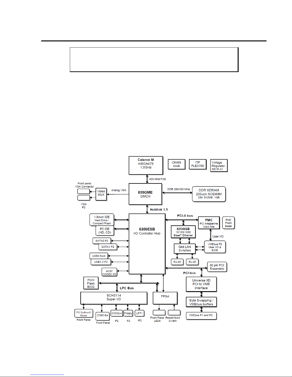
Operational Description
Figure 1-1 XVME 689-VR7 Block Diagram

Introduction
1-7
Environmental Specifications
The XVME 689-VR7 will meet the following environmental requirements:
Environmental Specification Operating Non-Operating
Thermal
-40 to 85 C
Humidity
10% to 90% RH,
non-condensing
10% to 90% RH, non-
condensing
Shock 30 g peak
acceleration, 11
msec duration
50 g peak acceleration,
11 msec duration
Vibration
5 – 2000 Hz
0.015” (0.38mm)
peak-to-peak
displacement, 2.5 g
maximum
acceleration
0.030” (0.76mm) peak-to-peak
displacement, 5 g maximum
acceleration
Emissions EN 55022 EN 55022
Immunity EN 50082-2 EN 50082-2
Introduction
1-8
Hardware Specifications
Characteristic Specification
Power Specifications: 5.4 A (typical); 10.5 A (maximum)
Voltage Specifications: +5V, +12V, -12V; all +5%/-2.5%
CPU speed: Intel Celeron M Low Power
Processor
1.8 GHz
L2 Cache: Intel Celeron M Low Power Processor 2 MB
Onboard memory SDRAM, up to 2 GB (one 200-pin SODIMM)
Integrated Graphics Controller 1600 x 1200 maximum resolution, 24-bit color maximum; 4 MB
Shared memory
Ethernet Controllers (2) Intel 82546GB 10/100/1000Base-TX Gigabit Ethernet; RJ-45
Mass Storage
Integrated SATA-150 Controller SATA0 and SATA1 via P2
EIDE Ultra DMA 100 interface 2 channels via P2
One 1.8" on-board EIDE via optional carrier module
Compact Flash One, on-board Compact flash site via optional carrier module
Floppy Drive Via P2 to XVME 977
PMC Site On board 66 MHz/64 Bit PMC/PCI-X with front and P0 I/O Access.
Site is 3.3V interface level
Optional 32bit / 33 MHz sites available via XVME-976-209 (2 sites,
total 3) and XVME-976-210 (4 sites, total 5)
Stereo Audio AD1981B AC97 CODEC, Line Level Stereo Input and Output Via
P2
USB One USB 2.0 via Front panel
Two USB 2.0 via P2
Serial Ports RS-232C, 16550 compatible (4) COM1 Front, Com 2 and 3 Rear
I/O, (Com 4 can be configured for RS-232/422/485 but only the
COM 4 out the P2, Com 2 and 3 are RS-232 only). The COM 4 out
the front is RS-232 data leads only.
Parallel Interface EPP/ECP compatible (1)
Keyboard and Mouse Via Front Panel
European Union – CE; Regulatory Compliance
Electromagnetic Compatibility - 89/336/EEC
RoHS Compliant product available
Introduction
1-9
VMEbus Specification
VMEbus Compliance
Complies with VMEbus Specification ANSI/VITA 1–1994
A32/A24/A16:D64/D32/D16/D08(EO) DTB Master
A32/A24/A16:D64/D32/D16/D08(EO) DTB Slave
R(0-3) Bus Requester
Interrupter I(1)-I(7) DYN
IH(1)-IH(7) Interrupt Handler
SYSCLK and SYSRESET Driver
PRI, SGL, RRS Arbiter
RWD, ROR bus release
Form Factor: DOUBLE 233.7 mm x 160 mm (9.2" x 6.3")
System Configuration and Expansion Options Tables
Table 1-2 XVME 689-VR7 CPU configurations
Ordering
Number
CPU Type
XVME 689-VR7/1XY Intel® Celeron® M 1.0GHz
Handle and P0 configurations Memory configurations
Y = 1 VME-64 IEEE 1101.1 (Std / legacy) handles w/o
VMEbus P0
X = 1 for 256 MB ECC DRR SDRAM
Y = 2 VME-64 IEEE 1101.10 (Compact PCI type) handles
w/o VMEbus P0
X = 2 for 512 MB ECC DRR SDRAM
Y = 3 VME-
64 IEEE 1101.1 (Std / legacy) handles with the
VMEbus P0
X = 3 for 1 GB ECC DRR SDRAM
Y = 4 VME-64 IEEE 1101.10 (Compact PCI type) handles
with the VMEbus P0
Note: Some features on the XVME 689-VR7 are only available in a 160-pin (5-Row) VMEbus P2
backplane.
The ordering number is broken into two parts. The model number is the 689-VR7. The tab number is the
three digits after the slash. For the XVME 689-VR7, the tab number indicates the CPU type, amount of
SDRAM memory (the middle digit) and the ejector handle type and optional P0 connector.
Introduction
1-10
.
Table 1-3 XVME 689-VR7 Expansion Module Options
Ordering Number Description
XVME 990-VR7/1
Drive Adapter Module for external drives, cables out back of VME
backplane, Primary PIDE (2 PIDE), Floppy, COM2 (Only RS-232),
two ports of SATA-150, LPT1, 1 USB port, Audio in/out and
Analog Video out plus P0 for rear I/O from PMC site and Ethernet
31.1 or rear RJ-45 Ethernet.
XVME 990-VR7/2
Drive Adapter Module for external drives, cables out back of VME
backplane, Primary PIDE (2 PIDE), Floppy, COM2 (Only RS-232),
two ports of SATA-150, LPT1, 1 USB port, Audio in/out and
Analog Video out
XVME-976-209
PMC Carrier module with two PMC module sites. The XVME-976209 allows for stacking of a second XVME-976-209, this
combination will accommodate a total of five PMC modules
XVME-977/011
Not Compatible with the XVME-689-VR7
XVME-979/1
Not Compatible with the XVME-689-VR7
XVME-979/2
Not Compatible with the XVME-689-VR7
XVME-979/3
Not Compatible with the XVME-689-VR7
XVME-979/4
Not Compatible with the XVME-689-VR7
XVME-979/5
Not Compatible with the XVME-689-VR7
XVME-979/6
Not Compatible with the XVME-689-VR7
XVME-9000-EXF
Not Compatible with the XVME-689-VR7
The XVME 990-VR7 is described in Chapter 5.
Installation and Setup
2-1
Chapter 2 – Installation and Setup
Board Layout
This chapter provides information on configuring the XVME 689-VR7 modules. It also provides information on
installing the XVME 689-VR7 into a backplane and enabling the Ethernet controller.
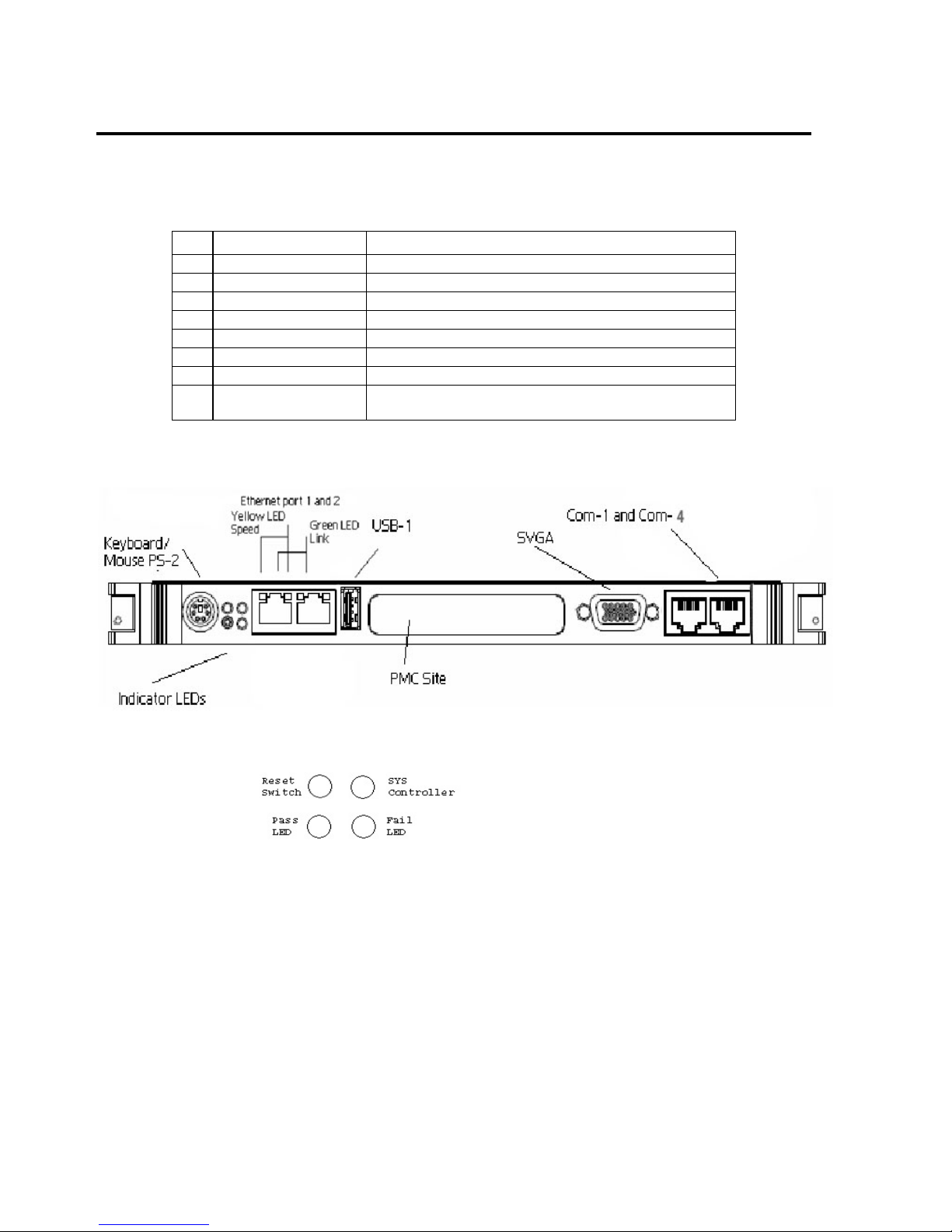
Fig. 2-1 shows the jumper, switch, and connector locations on the XVME 689-VR7.

Installation and Setup
2-2
3
Jumper Settings
The following table Lists XVME689-VR7 jumpers, their default positions, and their functions.
Table 2-1 XVME 689-VR7 Jumper Settings
Jumper Position Function
JP2
A
B √√√√
XVME 689-VR7 cannot generate SYSFAIL*
XVME 689-VR7 generates SYSFAIL* normally
JP32
A
B √√√√
Disables system resources (no auto SYSCON)
Enables system resources (auto SYSCON)
JP4
A √√√√
B
XVME 689-VR7 can reset VMEbus
XVME 689-VR7 cannot reset VMEbus
JP5
A √√√√
B
Normal
Clear CMOS
JP6
A √√√√
B
Boot from FLASH
Boot from ROM
JP7
A
B √√√√
Orb ground not connected to logic ground
Orb ground connected to logic ground
JP8
A √√√√
B
Normal (Video out Front Panel VGA)
Video re-routed to P2 connector (no video out front
panel)
JP60
1 ----- 2
3 4
5 6
SIO_COM_RXD 4 = RXD4
SIO_COM_RXD 4 = RXD422
SIO_COM_RXD 4 = RXD485
JP61
1 ----- 2
2 3
4 ----- 5
5 6
7 ----- 8
8 9
10 ----11
11 12
DCD4
485TXDDSR4
485TXD+
RI4
485RXDDTR4
485RXD+
JP62
A
√√√√
B
RS-232
RS-422/RS-485
denotes default
Installation and Setup
2-3
Switch Settings
The XVME 689-VR7 has one four-pole switch (SW1) shown in Figure 2-2. The switches
functions are explained in table 2-2. This switch controls the system response to the front panel
Abort switch. Figure 2-2 shows the switch settings required to reset on the XVME 689-VR7
CPU, to reset only the VME backplane, or to reset both. The XVME 689-VR7 is shipped with
all four switches in the closed position (which causes the push button reset switch to reset both
the XVME 689-VR7 and the VME backplane).
Figure. 2-2
SW1 XVME 689-VR7 has a 4 position DIP switch to control the following functions.
Table 2-2 Four-Pole Switch (SW1) Functions
Position
Open Closed
1
Do not respond to SYSRESET* Respond to SYSRESET*
2 Toggle switch does not cause SYSRESET* Toggle switch causes SYSRESET*
3
SYSFAIL* asserted on Power Up SYSFAIL* not asserted on Power
4
No local reset Toggle switch causes local reset
Registers
The XVME 689-VR7 modules contain the following Xembedded-defined I/O registers: 218h,
219h, 233h, and 234h.
Register 218h – Abort/CMOS Clear Register
This register controls the abort toggle switch and allows you to read the CMOS clear jumper
(main board J21).
Table 2-3 Abort/CMOS Clear Register Settings
Bit Signal Result R/W
0 RESERVED Reserved
1 RESERVED Reserved
2 RESERVED Reserved
3 RESERVED Reserved
4 ABORT_STS 1 = Abort toggle switch caused interrupt R
5 ABORT_CLR 0 = Clear and disable abort
1 = Enable abort
R/W
6 RESERVED Reserved
7 CLRCMOS 0 = Clear CMOS
1 = CMOS okay
R
Installation and Setup
2-4
Register 219h – Flash Control Register
This register controls the following LEDs and signals.
Table 2-4 LED/BIOS Register Settings
Bit LED/Signal Result R/W
01 FAULT 0 = Fault LED on
1 = Fault LED off
R/W
1 PASS 0 = PASS LED off
1 = PASS LED on
R/W
21 N/A N/A
3 N/A N/A
41 RESERVED Reserved
51 RESERVED Reserved
61 RESERVED Reserved
71 RESERVED Reserved
Register 233h – Watchdog Timer Register
This register controls watchdog timer operation.
Table 2-5 Watchdog Timer Register Settings
Bit Signal Result
0 RESERVED Reserved
1 RESERVED Reserved
2 RESERVED Reserved
3 RESERVED Reserved
4 WDOG_EN 1 = Enables the watchdog timer
5 MRESET_EN 1 = Timeout generates
0 = Timeout generates IRQ10
6 WDOG_STS Watchdog timer status bit
7 WDOG_CLR Toggling this bit clears the watchdog timer
back to a zero count.
Note
Before enabling the watchdog timer for the first time, it is necessary to reset the
count back to zero by toggling bit 7 (WDOG_CLR). Toggling implies changing
the state of bit (0 to 1 or 1 to 0).
Installation and Setup
2-5
Register 234h – Flash Paging and Byte Swap Register
This register controls access to the Flash paging and byte-swapping functions.
Table 2-6 Flash Paging and Byte Swap Register Settings
Bit Signal Result
0 FLB_A15 Flash address 15 - page control bit
1 FLB_A16 Flash address 16 - page control bit
2 FLB_A17 Flash address 17 - page control bit
3 Unused – set to 0 Do not use.
4 Unused – set to 0 Do not use.
5 Unused – set to 0 Do not use.
6 SWAPS 1 = No swapping (data invariant) occurs during slave cycles
7 SWAPM 1 = No swapping (data invariant) occurs during master cycles
Front Panel Layout
Panel LEDs and Switch
The reset switch can be enabled to reset see the setup of Sw-1 shown in Figure 2-2 and table 2-2. This switch can
be configured to either just reset the XVME 689-VR7 or to reset both the VMEbus and the XVME 689-VR7.
The green pass and red fail LEDs are used as an indication of board health during the BIOS boot up. Both the
green pass and red fail LEDs will light during the POST of the board. As the BIOS complete the POST, the red
fail LED will be turned off. This is an indication the XVME 689-VR7 has passed the POST. The Green SYS
Controller LED is lit when the XVME 689-VR7 is configured as the VMEbus system controller. This is the
function that grants bus ownership to multiple bus VME masters and provides the 16MHz clock signal on the
back plane.
Installation and Setup
2-6
Connectors
This section provides pin outs for the XVME 689-VR7 connectors. Refer to the EMC warning at
the beginning of this manual before attaching cables.
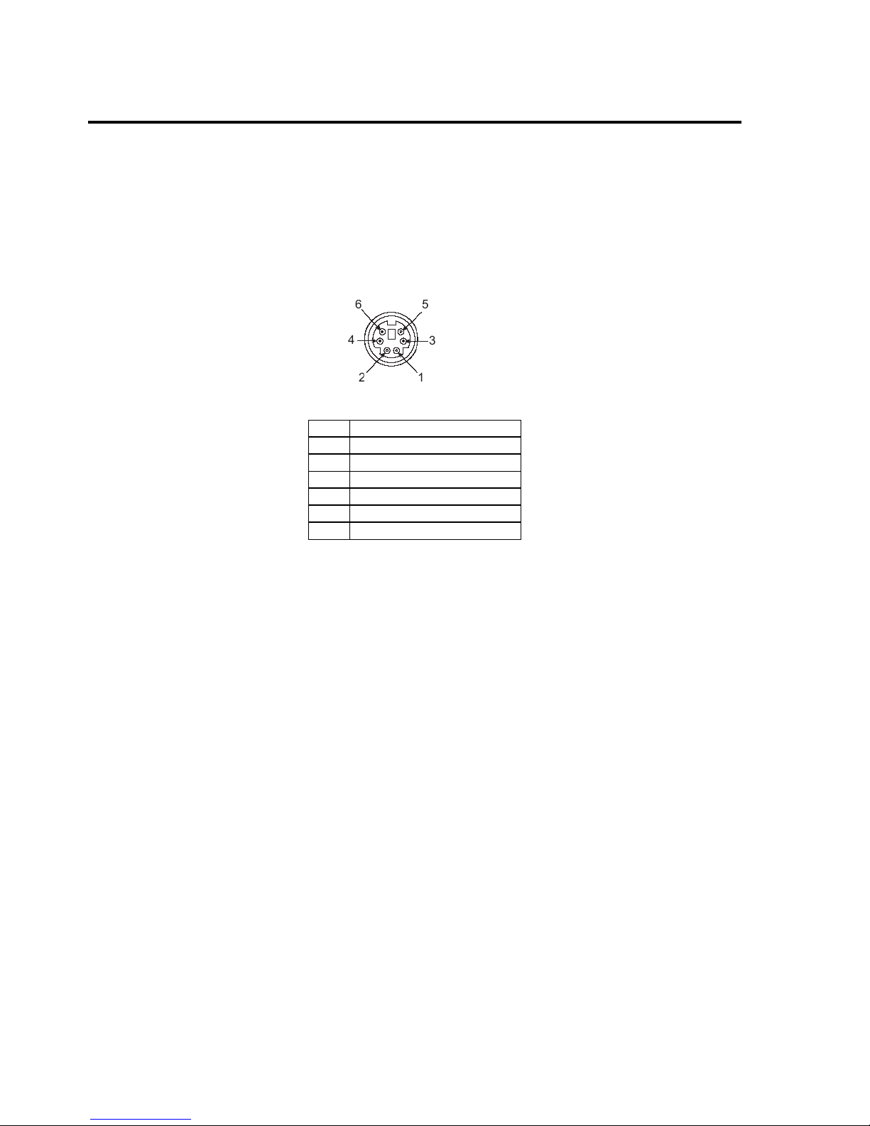
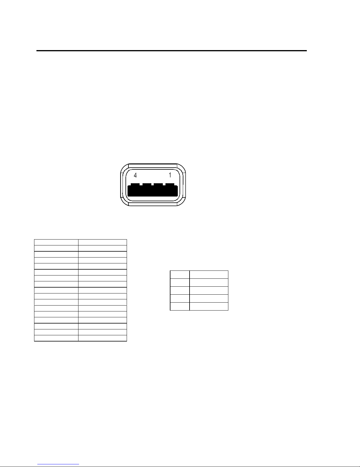
Keyboard/Mouse Port Connector (P7)
Figure 2-7
Table 2-7 Keyboard Port Connector Pin out
Pin Signal
1 Keyboard Data
2 Mouse Data
3 GND
4 +5V
5 Keyboard Clock
6 Mouse Clock
Installation and Setup
2-7
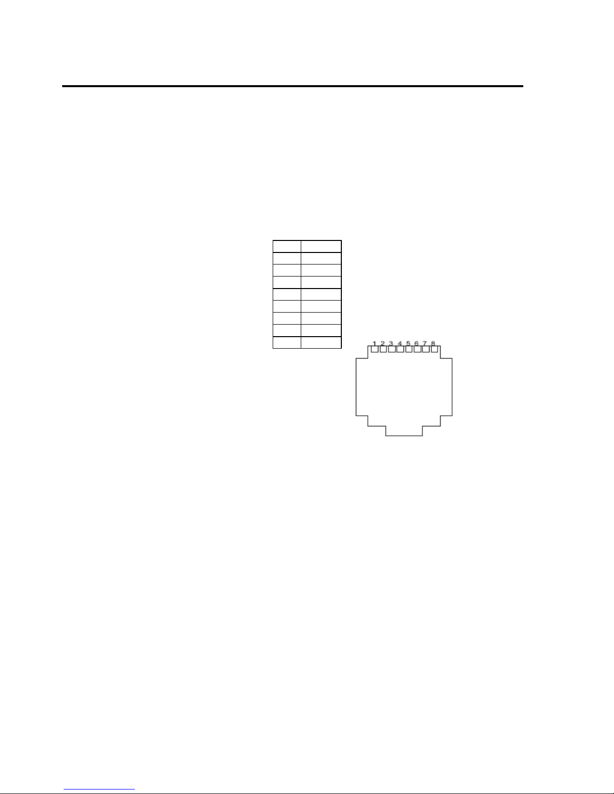
Front panel (P12), Rear Transition Module and Vita 31.1 Ethernet
____________________________________________________________
The Ethernet ports on the XVME 689-VR7 are switch able between the front and the rear of the XVME 689VR7. When in the rear mode, the Ethernet ports can use the (optional, available at order time only) PO
connector for either Vita 31.1 switch fabric over the Vita 31.1 compliant backplane or Ethernet out the XVME
990-VR7/2 rear transition module. The Vita 31.1 and the rear transition module can not supply Ethernet at the
same time, if a Vita 31.1 compliant backplane is in use then the rear transition module RJ-45s must not be
used.
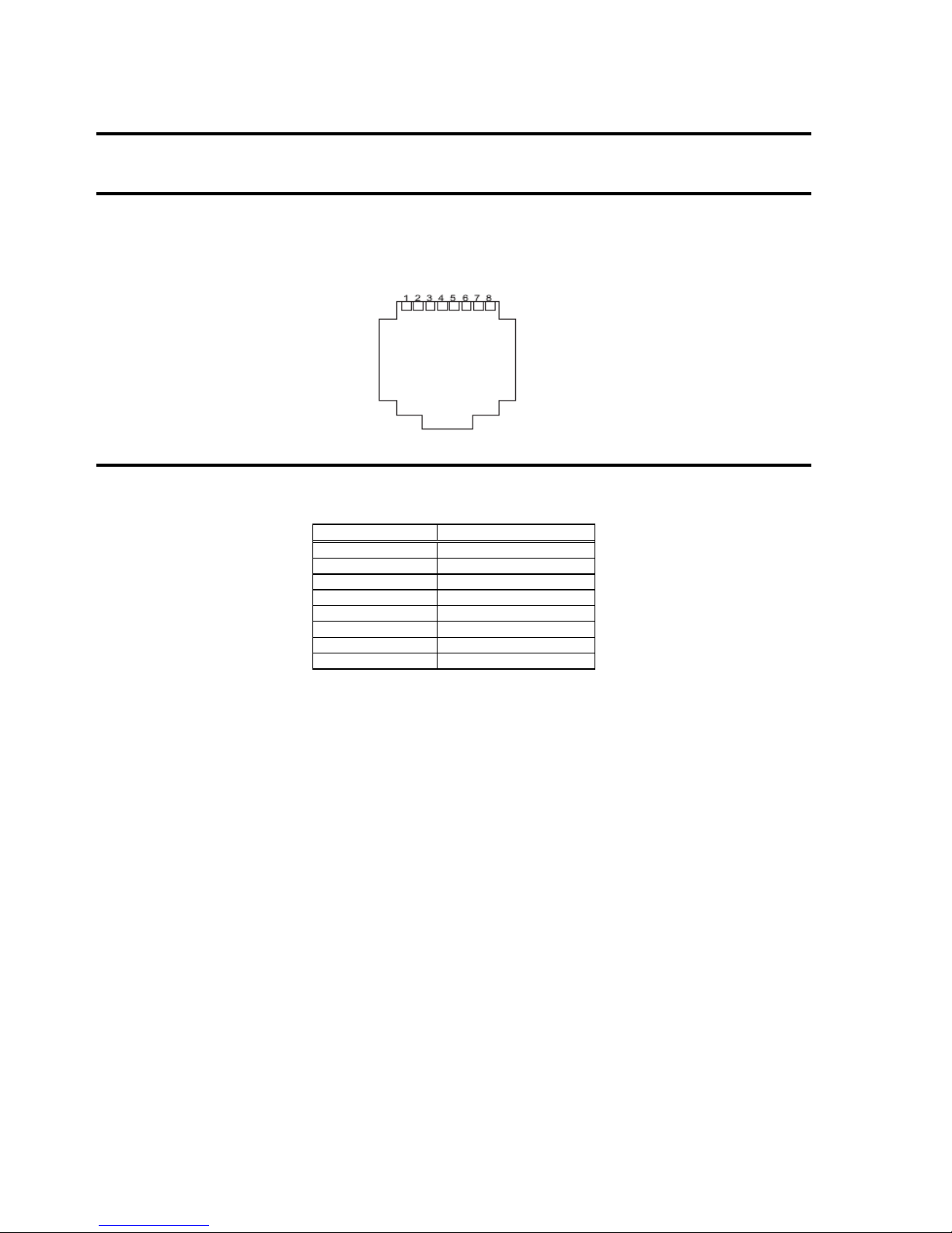
Table 2-8 RJ-45 10/100/1000 BaseT Connector Pin out
Figure 2-8 RJ-45 10/100/1000Mbps
Pin Signal
1 TX+
2 TX3 RX+
4 GND
5 GND
6 RX7 GND
8 GND
Installation and Setup
2-8
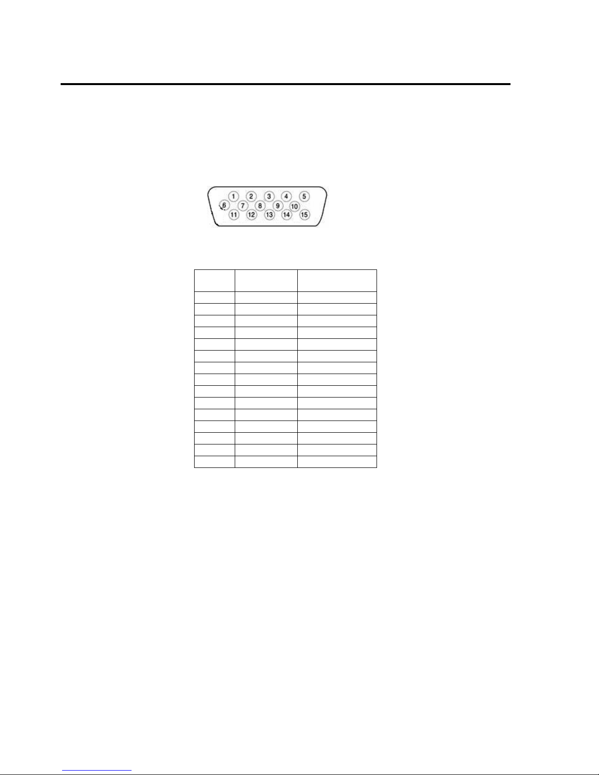
VGA Connector (P9)
The video is BIOS selectable and is available on either the front panel on a standard SVGA connector or out the
VMEbus P2. The table below shows the pin out of the standard video connector and also the VMEbus P2 pin out
for the rear access of video. The XVME 990-VR7 rear transition module connects to the rear of the VMEbus in
the same slot as the XVME 689-VR7 and allows for standard connections to off board devices. The XVME 990VR7 provides a standard SVGA connector for rear access.
Figure 2-9 SVGA Connector
Table 2-9 VGA Connector Pin out
SVGA
Pin out
Signal VMEbus P2
1 RED Row d Pin-20
2 GREEN Row d Pin-21
3 BLUE Row d Pin-22
4 NC N/C
5 GND Row d Pin-31
6 GND Row d Pin-31
7 GND Row d Pin-31
8 GND Row d Pin-31
9 25MIL_VIDA N/C
10 GND Row d Pin-31
11 NC N/C
12 LDDCDAT Row d Pin-26
13 HSYNC Row d Pin-23
14 VSYNC Row d Pin-24
15 LDDCCLK Row d Pin-25
Installation and Setup
2-9
USB Port Connector (J5)
USB provides an expandable, hot-pluggable Plug and Play serial interface that ensures a
standard, low-cost connection for peripheral devices. Devices suitable for USB range from
simple input devices such as keyboards, mice, and joysticks, to advanced devices such as
printers, scanners, storage devices, modems, and video conferencing cameras. USB 2.0 has a
raw data rate at 480Mbps, and it is rated 40 times faster than its predecessor interface, USB 1.1,
which tops at 12Mbps.
USB port 1 is available on the front panel using a standard connector as shown in Figure 2-10
below. The other two USB ports USB-2 and 3, are routed out the VMEbus P2 connector and can
be accesses either directly off the VMEbus P2 connector using the pin assignment shown in Fig.
2-10. The USB +5 V supplies are protected with a polyswitch. This device will open up if +5 V
is shorted to GND. Once the shorting condition is removed, the polyswitch will allow current
flow to resume.
Figure 2-10 USB Connector
Table 2-10 USB Port Connector Pin out
Table 2-11 Rear USB ports 2 and 3
USB Port Connector Pin out on VMEbus P2
VMEbus P2 Signal Name
P2-row-z 17 USB3_GND
P2-row-z 18 GND
P2-row-z 19 USB3+
P2-row-z 20 GND
P2-row-z 21 USB3P2-row-z 22 GND
P2-row-z 23 USB3_PWR
P2-row-z 24 GND
P2-row-z 25 USB2_GND
P2-row-z 26 GND
P2-row-z 27 USB2+
P2-row-z 28 GND
P2-row-z 29 USB2P2-row-z 30 GND
P2-row-z 31 USB2_PWR
P2-row-z 32 GND
Pin Signal
1 +5V
2 USBP03 USBP0+
4 GND
Installation and Setup
2-10
COM1 and COM4 (J4) Pin Definitions
The XVME 689-VR7 has two serial ports out the front panel, Com 1 and Com 4, these two com ports use the RJ45 connector. Two more com ports are out the VMEbus P2 connector and when the XVME 990-VR7 rear
transition module is in place com port 2 and 3 uses a DB-9 connector. See below for connector layout and pin
descriptions.
Figure 2-11 RJ-45 Serial Port Connectors
Com ports 1 and 4 Pin Definitions for front connectors
Pin Number RS232
1 RTS
2 DTR
3 TXD
4 GND
5 GND
6 RXD
7 DSR
8 CTS
Table 2-13 Serial Port Connector Pin out for Comm-1 and 4
Installation and Setup
2-11
On-Board Hard Drive/Compact Flash Site (J17)
A horizontal ZIF connector is used on the board. (Samtec part number ZF5-40-01-TM-WT.) The
connector on the board has a reverse pin out because of the connector orientation relative to the hard
drive. This allows the flex cable to loop up to the hard drive, with the connector side facing the board.
Table 2-14 On-Board storage devices us the J17 1.8inch Hard Drive Connector pin assignment
Pin # Description Pin # Description Pin # Description Pin # Description
1 factory use 11 DD4 21 GROUND 31 DA1
2 factory use 12 DD11 22 DMARQ 32 PDIAG3 RESET- 13 DD3 23 GROUND 33 DA0
4 GROUND 14 DD12 24 DIOW- 34 DA2
5 DD7 15 DD2 25 DIOR- 35 CS06 DD8 16 DD13 26 GROUND 36 CS17 DD6 17 DD1 27 IORDY 37 DASP8 DD9 18 DD14 28 GROUND 38 3.3V
9 DD5 19 DD0 29 DMACK- 39 3.3V
10 DD10 20 DD15 30 INTRQ 40 DEVADR
The Hitachi C4K60 CE has a 40 pin ZIF connector.
Table 2-15 1.8inch Hard Drive Connector pin assignment on hard drive
Pin # Description Pin # Description Pin # Description Pin # Description
40 factory use 30 DD4 20 GROUND 10 DA1
39 factory use 29 DD11 19 DMARQ 9 PDIAG38 RESET- 28 DD3 18 GROUND 8 DA0
37 GROUND 27 DD12 17 DIOW- 7 DA2
36 DD7 26 DD2 16 DIOR- 6 CS035 DD8 25 DD13 15 GROUND 5 CS134 DD6 24 DD1 14 IORDY 4 DASP33 DD9 23 DD14 13 GROUND 3 3.3V
32 DD5 22 DD0 12 DMACK- 2 3.3V
31 DD10 21 DD15 11 INTRQ 1 DEVADR
Installation and Setup
2-12
VMEbus Connectors
VMEbus P1 Connector
Table 2-16 P1 Connector Pin out
Pin Z A B C D
1*
MPR
D00 BBSY* D08 +5V
2 GND D01 BCLR* D09 GND
3*
MCLK
D02 ACFAIL*
D10
+V1
4 GND D03 BG0IN* D11
+V2
5*
MSD
D04 BG0OUT* D12
RSVU1
6 GND D05 BG1IN*
D13
-V1
7*
MMD
D06 BG1OUT* D14
-V2
8 GND D07 BG2IN* D15
RSVU2
9*
MCTL
GND BG2OUT*
GND
GAP*
10 GND SYSCLK BG3IN* SYSFAIL*
GA0*
11*
RESP*
GND BG3OUT* BERR*
GA1*
12 GND DS1* BR0* SYSR
E
SET*
13
SDB14*
DS0* BR1* LWORD*
GA2*
14 GND WRITE* BR2* AM5
15
SDB15*
GND BR3* A23
GA3*
16 GND DTACK* AM0 A22
17
SDBP1
GND AM1 A21
GA4*
18 GND AS* AM2 A20
19
RSVBUS5
GND AM3 A19
RSVBU1
20 GND IACK* GND A18
21
RSVBUS6
IACKIN*
NC
A17
RSVBU2
22 GND IACKOUT* NC A16
23
RSVBUS7
AM4 GND A15
RSVBU3
24 GND
A07 IRQ7*
A14
25
RSVBUS8
A06 IRQ6* A13
RSVBU4
26 GND A05 IRQ5* A12
27
RSVBUS9
A04 IRQ4*
A11
LI/I*
28 GND A03 IRQ3* A10
29
RSVBUS10
A02 IRQ2*
A09
LI/O*
30 GND A01 IRQ1*
A08
31
RSVBUS11
-12V NC +12V GND
32 GND +5V +5V +5V +5V
Some pins in columns Z and D are use internally as test points, these are denoted by italics. These pins are not
intended to drive any external devices and MUST not be used for any purpose.
 Loading...